

Datasheet dsPIC33EV64GM002, dsPIC33EV64GM102, dsPIC33EV128GM002, dsPIC33EV128GM102, dsPIC33EV256GM002 Datasheet
...Page 1

dsPIC33EVXXXGM00X/10X FAMILY
16-Bit, 5V Digital Signal Controllers with
PWM, SENT, Op Amps and Advanced Analog Features
Operating Conditions
• 4.5V to 5.5V, -40°C to +85°C, DC to 70 MIPS
• 4.5V to 5.5V, -40°C to +125°C, DC to 60 MIPS
• 4.5V to 5.5V, -40°C to +150°C, DC to 40 MIPS
Core: 16-Bit dsPIC33E CPU
• Code-Efficient (C and Assembly) Architecture
• 16-Bit Wide Data Path
• Two 40-Bit Wide Accumulators
• Single-Cycle (MAC/MPY) with Dual Data Fetch
• Single-Cycle, Mixed-Sign MUL plus Hardware
Divide
• 32-Bit Multiply Support
• Intermediate Security for Memory:
- Provides a Boot Flash Segment in addition to
the existing General Flash Segment
• Error Code Correction (ECC) for Flash
• Added Two Alternate Register Sets for Fast
Context Switching
Clock Management
• Internal, 15% Low-Power RC (LPRC) – 32 kHz
• Internal, 1% Fast RC (FRC) – 7.37 MHz
• Internal, 10% Backup RC (BFRC) – 7.37 MHz
• Programmable PLLs and Oscillator Clock Sources
• Fail-Safe Clock Monitor (FSCM)
• Additional FSCM Source (BFRC), Intended to
Provide a Clock Fail Switch Source for the
System Clock
• Independent Watchdog Timer (WDT)
• System Windowed Watchdog Timer (DMT)
• Fast Wake-up and Start-up
Power Management
• Low-Power Management modes (Sleep, Idle
and Doze)
• Power Consumption Minimized Executing
NOP String
• Integrated Power-on Reset (POR) and Brown-out
Reset (BOR)
• 0.5 mA/MHz Dynamic Current (typical)
• 50 µA at +25°C I
PD Current (typical)
PWM
• Up to Six Pulse-Width Modulation (PWM) Outputs
(three generators)
• Primary Master Time Base Inputs allow
Time Base Synchronization from Internal/External
Sources
• Dead Time for Rising and Falling Edges
• 7.14 ns PWM Resolution
• PWM Support for:
- DC/DC, AC/DC, inverters, Power Factor
Correction (PFC) and lighting
- Brushless Direct Current (BLDC), Permanent
Magnet Synchronous Motor (PMSM),
AC Induction Motor (ACIM), Switched
Reluctance Motor (SRM)
- Programmable Fault inputs
- Flexible trigger configurations for
Analog-to-Digital conversion
- Supports PWM lock, PWM output chopping
and dynamic phase shifting
Advanced Analog Features
• ADC module:
- Configurable as 10-bit, 1.1 Msps with
four S&H or 12-bit, 500 ksps with one S&H
- Up to 36 analog inputs
• Flexible and Independent ADC Trigger Sources
• Up to Four Op Amp/Comparators with Direct
Connection to the ADC module:
- Additional dedicated comparator and
7-bit Digital-to-Analog Converter (DAC)
- Two comparator voltage reference outputs
- Programmable references with 128 voltage
points
- Programmable blanking and filtering
• Charge Time Measurement Unit (CTMU):
- Supports mTouch™ capacitive touch sensing
- Provides high-resolution time
measurement (1 ns)
- On-chip temperature measurement
- Temperature sensor diode
- Nine sources of edge input triggers (CTED1,
CTED2, OCPWM, TMR1, SYSCLK, OSCLK,
FRC, BFRC and LPRC)
2013-2014 Microchip Technology Inc. DS70005144C-page 1
Page 2

dsPIC33EVXXXGM00X/10X FAMILY
Timers/Output Compare/Input Capture
• Nine General Purpose Timers:
- Five 16-bit and up to two 32-bit
timers/counters; Timer3 can provide ADC
trigger
• Four Output Capture modules Configurable as
Timers/Counters
• Four Input Capture modules
Communication Interfaces
• Two Enhanced Addressable Universal
Asynchronous Receiver/Transmitter (UART)
modules (6.25 Mbps):
- With support for LIN/J2602 bus support and
®
IrDA
- High and low speed (SCI)
• Two SPI modules (15 Mbps):
- 25 Mbps data rate without using PPS
•One I
• Two SENT J2716 (Single-Edge Nibble
• One CAN module:
2
C™ module (up to 1 Mbaud) with SMBus
Support
Transmission-Transmit/Receive) module for
Automotive Applications
- 32 buffers, 16 filters and three masks
Direct Memory Access (DMA)
• 4-Channel DMA with User-Selectable Priority
Arbitration
• UART, Serial Peripheral Interface (SPI), ADC,
Input Capture, Output Compare and Controller
Area Network (CAN)
Input/Output
• GPI/O Registers to Support Selectable
Slew Rate I/O
• Peripheral Pin Select (PPS) to allow Function
Remap
• Sink/Source: 8 mA or 12 mA, Pin-Specific for
Standard V
• Selectable Open-Drain, Pull-ups and Pull-Downs
• Change Notice Interrupts on All I/O Pins
OH/VOL
Qualification and Class B Support
• AEC-Q100 REVG (Grade 1: -40°C to +125°C)
Completed
• AEC-Q100 REVG (Grade 0: -40°C to +150°C)
Planned
• Class B Safety Library, IEC 60730
Class B Fault Handling Support
• Backup FRC
• Windowed WDT uses LPRC
• Windowed Deadman Timer (DMT) uses System
Clock (System Windowed Watchdog Timer)
• H/W Clock Monitor Circuit
• Oscillator Frequency Monitoring through CTMU
(OSCI, SYSCLK, FRC, BFRC, LPRC)
• Dedicated PWM Fault Pin
• Lockable Clock Configuration
Debugger Development Support
• In-Circuit and In-Application Programming
• Three Complex and Five Simple Breakpoints
• Trace and Run-Time Watch
DS70005144C-page 2 2013-2014 Microchip Technology Inc.
Page 3

2013-2014 Microchip Technology Inc. DS70005144C-page 3
dsPIC33EVXXXGM00X/10X PRODUCT FAMILIES
The device names, pin counts, memory sizes and peripheral availability of each device are listed in Tab le 1. The following pages show the devices’ pinout diagrams.
TABLE 1: dsPIC33EVXXXGM00X/10X FAMILY DEVICES
Device
SRAM Bytes
Program Memory Bytes
dsPIC33EV64GM002
dsPIC33EV64GM102 1
dsPIC33EV128GM002
dsPIC33EV128GM102 1
dsPIC33EV256GM002
dsPIC33EV256GM102 1
dsPIC33EV64GM004
dsPIC33EV64GM104 1
dsPIC33EV128GM004
dsPIC33EV128GM104 1
dsPIC33EV256GM004
dsPIC33EV256GM104 1
dsPIC33EV64GM006
dsPIC33EV64GM106 1
dsPIC33EV128GM006
dsPIC33EV128GM106 1
dsPIC33EV256GM006
dsPIC33EV256GM106 1
64K 8K
128K 8K
256K 16K
64K 8K
128K 8K
256K 16K
64K 8K
128K 8K
256K 16K
C™
SPI
CAN
32-Bit Timers
DMA Channels
16-Bit Timers (T1)
0
0
452443x222121113/41IntermediateY21328
0
0
0
452443x222121244/51IntermediateY35344 TQFP, QFN
0
0
0
452443x222121364/51IntermediateY53364 TQFP, QFN
0
Input Capture
PWM
UART
Output Compare
2
I
SENT
10/12-Bit ADC
ADC Inputs
CTMU
Op Amp/Comparators
Security
Peripheral Pin Select (PPS)
General Purpose I/O (GPIO)
Pins
External Interrupts
SPDIP, SOIC,
Packages
dsPIC33EVXXXGM00X/10X FAMILY
QFN-S
Page 4

dsPIC33EVXXXGM00X/10X FAMILY
28-Pin SPDIP/SOIC
(1,2,3)
MCLR
AVDD
AVSS
RPI47/PWM1L1/T5CK/RB15
PGED3/OA2IN-/AN2/C2IN1-/SS1
/RPI32/CTED2/RB0
RPI46/PWM1H1/T3CK/RB14
PGEC3/OA1OUT/A N3/C1IN4-/C4IN2-/ RPI33/CTED1/RB1
RPI45/PWM1L2/CTPLS/RB13
PGEC1/OA1IN+/AN4/C1IN3-/C1IN1+/C2IN3-/RPI34/RB2
RPI44/PWM1H2/RB12
PGED1/OA1IN-/AN5/C1IN1-/CTMUC/RP35/RB3
RP43/PWM1L3/RB11
RP42/PWM1H3/RB10
OSC1/CLKI/AN32/RPI18/RA2 V
CAP
OSC2/CLKO/RPI19/RA3
V
SS
FLT32/RP36/RB4
OA5IN-/AN27/C5IN1-/ASDA1/SDI1/RP41/RB9
OA5IN+/AN24/C5IN3-/C5IN1+/C4IN1+/RP20/T1CK/RA4 AN26/CV
REF1O/CVREF2O/ASCL1/SDO1/RP40/T4CK/RB8
V
DD
OA5OUT/AN25/C5IN4-/SCK1/RP39/INT0/RB7
PGED2/SDA1/RP37/RB5 PGEC2/SCL1/RP38/RB6
V
SS
OA2OUT/AN0/C2IN4-/C4IN3-/RPI16/RA0
OA2IN+/AN1/C2IN1+/RPI17/RA1
dsPIC33EV128GM002/102
dsPIC33EV64GM002/102
dsPIC33EV256GM002/102
1
2
3
4
5
6
7
8
9
10
11
12
13
14
28
27
26
25
24
23
22
21
20
19
18
17
16
15
Note 1: The RPn/RPIn pins can be used by any remappable peripheral with some limitation. See Section 11.5 “Peripheral
Pin Select (PPS)” for available peripherals and information on limitations.
2: Every I/O port pin (RAx-RGx) can be used as a Change Notification pin (CNAx-CNGx). See Section 11.0 “I/O
Ports” for more information.
3: If the op amp is selected when OPAEN (CMxCON<10>) = 1, the OAx input is used; otherwise, the ANx input is
used.
Pin Diagrams
DS70005144C-page 4 2013-2014 Microchip Technology Inc.
Page 5

Pin Diagrams (Continued)
28-Pin QFN-S
(1,2,3,4)
dsPIC33EV 64GM002/102
dsPIC33EV 128GM002/102
dsPIC33EV256GM002/102
28 27 26 25 24 23 22
89
10 11 12 13 14
3
18
17
16
15
4
5
7
1
2
20
19
6
21
OA5OUT/AN25/C5IN4-/SCK1/RP39/INT0/RB7
PGEC2/SCL1/RP38/RB6
PGED2/SDA1/RP37/RB5
V
DD
OA 5 IN+/AN24/C5IN3-/C5 IN1+/C4IN1+/RP20/T1CK/RA4
FLT32/RP36/RB4
RPI45/PWM1L2/CTPLS/RB13
RPI44/PWM1H2/RB12
RP43/PWM1L3/RB11
RP42/PWM1H3/RB10
V
CAP
VSS
OA5IN-/AN27/C5IN1-/ASDA1/SDI1/RP41/RB9
RPI46/PWM1H1/T3CK/RB14
RPI47/PWM1L1/T5CK/RB15
AVSSAVDD
MCLR
PGED3/OA2IN-/AN2/C21N1-/SS1/RPI32/CTED2/RB0
PGEC3/OA1OUT/AN3/C1IN4-/C4IN2-/RPI33/CTED1/RB1
V
SS
OSC1/CLKI/AN32/RPI18/RA2
OSC2/CLKO/RPI19/RA3
PGEC1/OA1IN+/AN4/C1IN3-/C1IN1+/C2IN3-/RPI34/RB2
PGED1/OA1IN-/AN5/C1IN1-/CTMUC/RP35/RB3
OA2OUT/AN0/C2IN4-/ C4IN3-/RPI16/RA0
OA2IN+/AN1/C2IN1+/RPI17/RA1
AN26/CVREF1O/CVREF2O/ASCL1/SDO1/RP40/T4CK/RB8
Note 1: The RPn/RPIn pins can be used by any remappable peripheral with some limitation. See Section 11.5 “Peripheral
Pin Select (PPS)” for available peripherals and information on limitations.
2: Every I/O port pin (RAx-RGx) can be used as a Change Notification pin (CNAx-CNGx). See Section 11.0 “I/O
Ports” for more information.
3: If the op amp is selected when OPAEN (CMxCON<10>) = 1, the OAx input is used; otherwise, the ANx input is
used.
4: The metal pad at the bottom of the device is not connected to any pins and is recommended to be connected to
V
SS externally.
dsPIC33EVXXXGM00X/10X FAMILY
2013-2014 Microchip Technology Inc. DS70005144C-page 5
Page 6

dsPIC33EVXXXGM00X/10X FAMILY
AN26/CV
REF1O
/ASCL1/RP40/T4CK/RB8
AN56/RA10
RPI45/PWM1L2/CTPLS/RB13
PGEC1/OA1IN+/AN4/C1IN3-/C1IN1+/C2IN3-/RPI34/RB2
PGED1/OA1IN-/AN5/C1IN1-/CTMUC/RP35/RB3
OA3OUT/AN6/C3IN4-/C4IN4-/C4IN1+/RP48/RC0
OA3IN-/AN7/C3IN1-/C4IN1-/RP49/RC1
OA3IN+/AN8/C3IN3-/C3IN1+/RPI50/U1RTS
/BCLK1/FLT3/RC2
V
DD
OSC1/CLKI/AN32/RPI18/RA2
OSC2/CLKO/RPI19/RA3
RPI24/RA8
FLT32/RP36/RB4
AN55/RA7
RPI46/PWM1H1/T3CK/RB14
RPI47/PWM1L1/T5CK/RB15
AV
SS
AV
DD
MCLR
OA2OUT/AN0/C2IN4-/C4IN3-/RPI16/RA0
OA2IN+/AN1/C2IN1+/RPI17/RA1
PGED3/OA2IN-/AN2/C2IN1-/SS1
/RPI32/CTED2/RB0
PGEC3/OA1OUT/AN3/C1IN4-/C4IN2-/RPI33/CTED1/RB1
RPI44/PWM1H2/RB12
RP43/PWM1L3/RB11
RP42/PWM1H3/RB10
V
CAP
V
SS
AN54/RP57/RC9
AN51/RP56/RC8
AN52/RP55/RC7
AN53/RP54/RC6
OA5IN-/AN27/C5IN1-/ASDA1/RP41/RB9
OA5OUT/AN25/C5IN4-/RP39/INT0/RB7
PGEC2/SCL1/RP38/RB6
PGED2/SDA1/RP37/RB5
VDDVSSAN31/CV
REF2O
/RPI53/RC5
AN30/CV
REF
+/RPI52/RC4
AN29/SCK1/RPI51/RC3
AN28/SDI1/RPI25/RA9
OA5IN+/AN24/C5IN3-/C5IN1+/SDO1/RP20/T1CK/RA4
1213141516171819202122
4443424140393837363534
31
30
29
28
27
26
25
24
23
33
32
1
2
3
4
5
6
7
8
9
10
11
V
SS
dsPIC33EV64GM004/104
dsPIC33EV128GM004/104
dsPIC33EV256GM004/104
Note 1: The RPn/RPIn pins can be used by any remappable peripheral with some limitation. See Section 11.5 “Peripheral
Pin Select (PPS)” for available peripherals and information on limitations.
2: Every I/O port pin (RAx-RGx) can be used as a Change Notification pin (CNAx-CNGx). See Section 11.0 “I/O
Ports” for more information.
3: If the op amp is selected when OPAEN (CMxCON<10>) = 1, the OAx input is used; otherwise, the ANx input is
used.
44-Pin TQFP
(1,2,3)
Pin Diagrams (Continued)
DS70005144C-page 6 2013-2014 Microchip Technology Inc.
Page 7

Pin Diagrams (Continued)
dsPIC33EV64GM004/104
dsPIC33EV128GM004/104
dsPIC33EV256GM004/104
43 42 41 40 39 38 37 36 35
12 13 14 15 16 17 18 19 20 21
3
30
29
28
27
26
25
24
23
4
5
7
8
9
10
11
1
2
32
31
6
22
33
34
AN26/CV
REF1O
/ASCL1/RP40/T4CK/RB8AN56/RA10
RPI45/PWM1L2/CTPLS/RB13
PGEC1/OA1IN+/AN4/C1IN3-/C1IN1+/C2IN3-/RPI34/RB2
PGED1/OA1IN-/ AN5/C1IN1-/CTMUC/RP35/RB3
OA3OUT/AN6/C3IN4-/C4IN4-/C4IN1+/RP48/RC0
OA3IN-/AN7/C3IN1-/C4IN1-/RP49/RC1
OA3IN+/AN8/C3IN3-/C3IN1+/RPI50/U1RTS
/BCLK1/FLT3/RC2
V
DD
V
SS
OSC1/CLKI/AN32/RPI18/RA2
OSC2/CLKO/RPI19/RA3
RPI24/RA8
FLT32/RP36/RB4
AN55/RA7
RPI46/PWM1H1/T3CK/RB14
RPI47/PWM1L1/T5CK/RB15
AV
SS
AV
DD
MCLR
OA2OUT/AN0/C2IN4-/C4IN3-/RPI16/RA0
OA2IN+/AN1/C2I N1+/RPI17/RA1
PGED3/OA2IN-/AN2/C2IN1-/SS1
/RPI32/CTE D2/RB0
PGEC3/OA1OUT/AN3/C1IN4-/C4IN2-/RPI33/CTED1/RB1
RPI44/PWM1H2/RB12
RP43/PWM1L3/RB11
RP42/PWM1H3/RB10
V
CAP
V
SS
AN54/RP57/RC9
AN51/RP56/RC8
AN52/RP55/RC7
AN53/RP54/RC6
OA5IN-/AN27/C5IN1-/ASDA1/RP41/RB9
OA5OUT/AN25/C5IN4-/RP39/INT0/RB7
PGEC2/SCL1/RP38/RB6
PGED2/SDA1/RP37/RB5
VDDVSSAN31/CV
REF2O
/RPI53/RC5
AN30/CV
REF
+/RPI52/RC4
AN29/SCK1/RPI 51/RC3
AN28/SDI1/RPI25/RA9
OA5IN+/AN24/C5IN3-/C5IN1+/SDO1/RP20/T1CK/RA4
44
44-Pin QFN
(1,2,3,4)
Note 1: The RPn/RPIn pins can be used by any remappable peripheral with some limitation. See Section 11.5 “Peripheral
Pin Select (PPS)” for available peripherals and information on limitations.
2: Every I/O port pin (RAx-RGx) can be used as a Change Notification pin (CNAx-CNGx). See Section 11.0 “I/O
Ports” for more information.
3: If the op amp is selected when OPAEN (CMxCON<10>) = 1, the OAx input is used; otherwise, the ANx input is
used.
4: The metal pad at the bottom of the device is not connected to any pins and is recommended to be connected to
V
SS externally.
dsPIC33EVXXXGM00X/10X FAMILY
2013-2014 Microchip Technology Inc. DS70005144C-page 7
Page 8

dsPIC33EVXXXGM00X/10X FAMILY
64-Pin TQFP
(1,2,3)
AN55/RA7
RPI46/PWM1H1/T3CK/RB14
RPI47/PWM1L1/T5CK/RB15
AN19/RP118/RG6
AN18/RPI119/RG7
AN17/RP120/RG8
MCLR
AN16/RPI121/RG9
V
SS
V
DD
AN10/RPI28/RA12
AN9/RPI27/RA11
OA2OUT/AN0/C2IN4-/C4IN3-/RPI16/RA0
OA2IN+/AN1/C2IN1+/RPI17/ RA1
PGED3/OA2IN-/AN2/C2IN1-/
SS1/RPI32/CTED2/RB0
PGEC3/OA1OUT/AN3/C1IN4-/C4IN2-/RPI33/CTED1/RB1
AN56/RA10
RPI45/PWM1L2/CTPLS/RB13
RPI44/PWM1H2/RB12
RP43/PWM1L3/RB11
RP42/PWM1H3/RB10
RP97/RF1
RPI96/RF0
VDDV
CAP
AN54/RP57/RC9
RP70/RD6
RP69/RD5
AN51/RP56/RC8
AN52/RP55/RC7
AN53/RP54/RC6
OA5IN-/AN27//C5IN1-/ASDA1/RP41/RB9
AN26/CV
REF1O
/ASCL1/RP40/T4CK/RB8
RPI61/RC13
OA5OUT/AN25/C5IN4-/RP39/INT0/RB7
AN48/CV
REF2O
/RPI58/RC10
PGEC2/SCL1/RP38/RB6
PGED2/SDA1/RP37/RB5
RPI72/RD8
V
SS
OSC2/CLKO/RPI63/RC15
OSC1/CLKI/AN49/RPI60/ RC12
V
DD
AN31/RPI53/RC5
AN30/CV
REF
+/RPI52/RC4
AN29/SCK1/ RPI51/RC3
AN28/SDI1/RPI25/RA9
OA5IN+/AN24/C5IN3-/C5IN1+/SDO1/RP20/T1CK/RA4
PGEC1/OA1IN+/AN4/C1IN3-/C1IN1+/C2IN3-/RPI34/RB2
PGED1/OA1IN- /AN5/C1IN1-/(CTMUC)/RP35/RB3
AV
DD
AV
SS
OA3OUT/AN6/C3I N4-/C4IN4-/C4IN1+/RP48/RC0
OA3IN-/AN7/C3IN1-/C4IN1-/RP49/RC1
OA3IN+/AN8/C3IN3-/C3IN1+/RPI50/
U1RTS/BCLK1/FLT3/RC2
AN11/C1IN2-/
U1CTS/FLT4/RC11
V
SS
V
DD
AN12/C2IN2-/C5IN2-/
U2RTS/BCLK2/FLT5/RE12
AN13/C3IN2-/
U2CTS/FLT6/RE13
AN14/RPI94/
FLT7/RE14
AN15/RPI95/
FLT8/RE15
RPI24/RA8
FLT32
/RP36/RB4
dsPIC33EV64GM006/106
dsPIC33EV128GM006/106
dsPIC33EV256GM006/106
646362616059585756
5
5
5453525150
49
1
48
2
47
3
46
4
45
5
44
6
43
7
42
8
41
9
40
10
39
11
38
12
37
13
36
14
35
15
34
16
33
171819202122232425262728293031
32
Note 1: The RPn/RPIn pins can be used by any remappable peripheral with some limitation. See Section 11.5 “Peripheral
Pin Select (PPS)” for available peripherals and information on limitations.
2: Every I/O port pin (RAx-RGx) can be used as a Change Notification pin (CNAx-CNGx). See Section 11.0 “I/O
Ports” for more information.
3: If the op amp is selected when OPAEN (CMxCON<10>) = 1, the OAx input is used; otherwise, the ANx input is
used.
Pin Diagrams (Continued)
DS70005144C-page 8 2013-2014 Microchip Technology Inc.
Page 9

Pin Diagrams (Continued)
64-Pin QFN
(1,2,3,4)
dsPIC33EV64GM006/106
dsPIC33EV128GM006/106
dsPIC33EV256GM006/106
646362616059585756555453525150
49
1
48
2
47
3
46
4
45
5
44
6
43
7
42
8
41
9
40
10
39
11
38
12
37
13
36
14
35
15
34
16
33
171819202122232425262728293031
32
AN56/RA10
RPI45/PWM1L2/CTPLS/RB13
RPI44/PWM1H2/RB12
RP43/PWM1L3/RB11
RP42/PWM1 H3/RB10
RP97/RF1
RPI96/RF0
VDDV
CAP
AN54/RP57/RC9
RP70/RD6
RP69/RD5
AN51/RP56/RC8
AN52/RP55/RC7
AN53/RP54/RC6
OA5IN-/AN27/C5IN1-/ASDA1/RP41/RB9
AN26/CV
REF1O
/ASCL1/RP40/T4CK/RB8
RPI61/RC13
OA5OUT/AN25/C5IN4-/RP39/INT0/RB7
AN48/CV
REF2O
/RPI58/RC10
PGEC2/SCL1/RP38/RB6
PGED2/SDA1/RP37/ RB5
RPI72/RD8
V
SS
OSC2/CLKO/RPI63/RC15
OSC1/CLKI/AN49/RPI60/RC12
V
DD
AN31/RPI53/RC5
AN30/CV
REF
+/RPI52/RC4
AN29/SCK1/RPI51/RC3
AN28/SDI1/RPI25/RA9
OA5
IN+/AN24/C5IN3-/C5IN1+/SDO1/RP20/T1CK/RA4
PGEC1/OA1IN+/AN4/C1IN3-/C1IN1+/C2IN3-/RPI34/RB2
PGED1/OA1IN-/AN5/C1IN1-/(CTMUC)/RP35/RB3
AV
DD
AV
SS
OA3OUT/AN6/C3IN4-/C4IN4-/C4IN1+/RP48/RC0
OA3IN-/AN7/C3IN1-/C4IN1-/RP49/RC1
OA3IN+/AN8/C3IN3-/C3IN1+/RPI50/U1RTS
/BCLK1/FLT3/RC2
AN11/C1IN2-/U1CTS
/FLT4/RC11
V
SS
V
DD
AN12/C2IN2-/C5IN2-/U2RTS/BCLK2/FLT5/RE12
AN13/C3IN2-/U2CTS
/FLT6/RE13
AN14/RPI94/FLT7/RE14
AN15/RPI95/FLT8/RE15
RPI24/RA8
FLT32/RP36/RB4
AN55/RA7
RPI46/PWM1H1/T3CK/RB14
RPI47/PWM1L1/T5CK/RB15
AN19/RP118/RG6
AN18/RPI119/RG7
AN17/RP120/RG8
MCLR
AN16/RPI121/RG9
V
SS
V
DD
AN10/RPI28/RA12
AN9/RPI27/RA11
OA2OUT/AN0/C2IN4-/C4IN3-/RPI16/RA0
OA2IN+/AN1/C2IN1+/RPI17/RA1
PGED3/OA2IN-/AN2/C2IN1-/
SS1/RPI32/CTED2/RB0
PGEC3/OA1OUT/AN3/C1IN4-/C4IN2-/RPI33/CTED1/RB1
Note 1: The RPn/RPIn pins can be used by any remappable peripheral with some limitation. See Section 11.5 “Peripheral
Pin Select (PPS)” for available peripherals and information on limitations.
2: Every I/O port pin (RAx-RGx) can be used as a Change Notification pin (CNAx-CNGx). See Section 11.0 “I/O
Ports” for more information.
3: If the op amp is selected when OPAEN (CMxCON<10>) = 1, the OAx input is used; otherwise, the ANx input is
used.
4: The metal pad at the bottom of the device is not connected to any pins and is recommended to be connected to
V
SS externally.
dsPIC33EVXXXGM00X/10X FAMILY
2013-2014 Microchip Technology Inc. DS70005144C-page 9
Page 10

dsPIC33EVXXXGM00X/10X FAMILY
Table of Contents
dsPIC33EVXXXGM00X/10X Product Families ...................................................................................................................................... 3
1.0 Device Overview ........................................................................................................................................................................ 13
2.0 Guidelines for Getting Started with 16-Bit Digital Signal Controllers.......................................................................................... 17
3.0 CPU............................................................................................................................................................................................ 21
4.0 Memory Organization ................................................................................................................................................................. 31
5.0 Flash Program Memory.............................................................................................................................................................. 81
6.0 Resets ....................................................................................................................................................................................... 89
7.0 Interrupt Controller ..................................................................................................................................................................... 93
8.0 Direct Memory Access (DMA) .................................................................................................................................................. 107
9.0 Oscillator Configuration............................................................................................................................................................ 121
10.0 Power-Saving Features............................................................................................................................................................ 131
11.0 I/O Ports ................................................................................................................................................................................... 141
12.0 Timer1 ...................................................................................................................................................................................... 171
13.0 Timer2/3 and Timer4/5 ............................................................................................................................................................ 173
14.0 Deadman Timer (DMT) ............................................................................................................................................................ 179
15.0 Input Capture............................................................................................................................................................................ 187
16.0 Output Compare....................................................................................................................................................................... 191
17.0 High-Speed PWM Module ....................................................................................................................................................... 197
18.0 Serial Peripheral Interface (SPI)............................................................................................................................................... 219
19.0 Inter-Integrated Circuit™ (I
20.0 Single-Edge Nibble Transmission (SENT) ............................................................................................................................... 235
21.0 Universal Asynchronous Receiver Transmitter (UART) .......................................................................................................... 245
22.0 Controller Area Network (CAN) Module (dsPIC33EVXXXGM10X Devices Only).................................................................... 251
23.0 Charge Time Measurement Unit (CTMU) ................................................................................................................................ 277
24.0 10-Bit/12-Bit Analog-to-Digital Converter (ADC) ...................................................................................................................... 283
25.0 Op Amp/Comparator Module ................................................................................................................................................... 299
26.0 Comparator Voltage Reference ................................................................................................................................................ 311
27.0 Special Features ...................................................................................................................................................................... 315
28.0 Instruction Set Summary .......................................................................................................................................................... 325
29.0 Development Support............................................................................................................................................................... 335
30.0 Electrical Characteristics .......................................................................................................................................................... 339
31.0 High-Temperature Electrical Characteristics............................................................................................................................ 401
32.0 Packaging Information.............................................................................................................................................................. 411
Appendix A: Revision History............................................................................................................................................................. 431
Index ................................................................................................................................................................................................. 433
The Microchip Web Site..................................................................................................................................................................... 439
Customer Change Notification Service .............................................................................................................................................. 439
Customer Support .............................................................................................................................................................................. 439
Product Identification System............................................................................................................................................................. 441
2
C™).............................................................................................................................................. 227
DS70005144C-page 10 2013-2014 Microchip Technology Inc.
Page 11

dsPIC33EVXXXGM00X/10X FAMILY
TO OUR VALUED CUSTOMERS
It is our intention to provide our valued customers with the best documentation possible to ensure successful use of your Microchip
products. To this end, we will continue to improve our publications to better suit your needs. Our publications will be refined and
enhanced as new volumes and updates are introduced.
If you have any questions or comments regarding this publication, please contact the Marketing Communications Department via
E-mail at docerrors@microchip.com. We welcome your feedback.
Most Current Data Sheet
To obtain the most up-to-date version of this data sheet, please register at our Worldwide Web site at:
http://www.microchip.com
You can determine the version of a data sheet by examining its literature number found on the bottom outside corner of any page.
The last character of the literature number is the version number, (e.g., DS30000000A is version A of document DS30000000).
Errata
An errata sheet, describing minor operational differences from the data sheet and recommended workarounds, may exist for current
devices. As device/documentation issues become known to us, we will publish an errata sheet. The errata will specify the revision
of silicon and revision of document to which it applies.
To determine if an errata sheet exists for a particular device, please check with one of the following:
• Microchip’s Worldwide Web site; http://www.microchip.com
• Your local Microchip sales office (see last page)
When contacting a sales office, please specify which device, revision of silicon and data sheet (include literature number) you are
using.
Customer Notification System
Register on our web site at www.microchip.com to receive the most current information on all of our products.
2013-2014 Microchip Technology Inc. DS70005144C-page 11
Page 12

dsPIC33EVXXXGM00X/10X FAMILY
Referenced Sources
This device data sheet is based on the following
individual chapters of the “dsPIC33/PIC24 Family
Reference Manual”, which are available from the
Microchip web site (www.microchip.com). The follow-
ing documents should be considered as the general
reference for the operation of a particular module or
device feature:
• “Introduction” (DS70573)
• “CPU” (DS70359)
• “Data Memory” (DS70595)
• “Program Memory” (DS70613)
• “Flash Programming” (DS70609)
• “Interrupts” (DS70000600)
• “Oscillator” (DS70580)
• “Reset” (DS70602)
• “Watchdog Timer and Power-Saving Modes” (DS70615)
• “I/O Ports” (DS70000598)
• “Timers” (DS70362)
• “CodeGuard™ Intermediate Security” (DS70005182)
• “Deadman Timer (DMT)” (DS70005155)
• “Input Capture” (DS70000352)
• “Output Compare” (DS70005157)
• “High-Speed PWM”(DS70645)
• “Analog-to-Digital Converter (ADC)” (DS70621)
• “Universal Asynchronous Receiver Transmitter (UART)” (DS70000582)
• “Serial Peripheral Interface (SPI)” (DS70005185)
• “Inter-Integrated Circuit™ (I
• “Enhanced Controller Area Network (ECAN™)”(DS70353)
• “Direct Memory Access (DMA)” (DS70348)
• “Programming and Diagnostics” (DS70608)
• “Op Amp/Comparator” (DS70000357)
• “Device Configuration” (DS70000618)
• “Charge Time Measurement Unit (CTMU)” (DS70661)
• “Single-Edge Nibble Transmission (SENT) Module” (DS70005145)
2
C™)” (DS70000195)
DS70005144C-page 12 2013-2014 Microchip Technology Inc.
Page 13

dsPIC33EVXXXGM00X/10X FAMILY
PORTA
Power-up
Timer
Oscillator
Start-up
OSC1/CLKI
MCLR
VDD, VSS
UART1/2
Timing
Generation
CAN1
(1)
I2C1
ADC
Timers
Input
Capture
Output
Compare
AV
DD, AVSS
SPI1/2
Watchdog
Timer/
POR/BOR
PWM
Remappable
Pins
Note 1: This feature or peripheral is only available on dsPIC33EVXXXGM10X devices.
CTMU
SENT1/2
CPU
Refer to Figure 3-1 for CPU diagram details.
16
16
PORTB
PORTC
PORTD
PORTE
PORTF
PORTG
PORTS
Peripheral Modules
Timer
Deadman
Op Amp/
Comparator
Timer
1.0 DEVICE OVERVIEW
This document contains device-specific information for
the dsPIC33EVXXXGM00X/10X family Digital Signal
Note 1: This data sheet summarizes the features
of the dsPIC33EVXXXGM00X/10X family
of devices. It is not intended to be a
comprehensive reference source. To
complement the information in this data
sheet, refer to the related section in the
“dsPIC33/PIC24 Family Reference Manual”, which is available from the Microchip
Controller (DSC) devices.
dsPIC33EVXXXGM00X/10X family devices contain
extensive Digital Signal Processor (DSP) functionality
with a high-performance, 16-bit MCU architecture.
Figure 1-1 shows a general block diagram of the core
and peripheral modules. Table 1-1 lists the functions of
the various pins shown in the pinout diagrams.
web site (www.microchip.com).
2: Some registers and associated bits
described in this section may not be
available on all devices. Refer to
Section 4.0 “Memory Organization” in
this data sheet for device-specific register
and bit information.
FIGURE 1-1: dsPIC33EVXXXGM00X/10X FAMILY BLOCK DIAGRAM
2013-2014 Microchip Technology Inc. DS70005144C-page 13
Page 14

dsPIC33EVXXXGM00X/10X FAMILY
TABLE 1-1: PINOUT I/O DESCRIPTIONS
Pin
Pin Name
AN0-AN35 I Analog No Analog input channels.
CLKI
CLKO
OSC1
OSC2
REFCLKO O — Yes Reference clock output.
IC1-IC4 I ST Yes Capture Inputs 1 to 4.
OCFA
OC1-OC4
INT0
INT1
INT2
RA0-RA4, RA7-RA12 I/O ST Yes PORTA is a bidirectional I/O port.
RB0-RB15 I/O ST Yes PORTB is a bidirectional I/O port.
RC0-RC13, RC15 I/O ST Yes PORTC is a bidirectional I/O port.
RD5-RD6, RD8 I/O ST Yes PORTD is a bidirectional I/O port.
RE12-RE15 I/O ST Yes PORTE is a bidirectional I/O port.
RF0-RF1 I/O ST No PORTF is a bidirectional I/O port.
RG6-RG9 I/O ST Yes PORTG is a bidirectional I/O port.
T1CK
T2CK
T3CK
T4CK
T5CK
CTPLS
CTED1
CTED2
U1CTS
U1RTS
U1RX
U1TX
U2CTS
U2RTS
U2RX
U2TX
SCK1
SDI1
SDO1
SS1
Legend: CMOS = CMOS compatible input or output Analog = Analog input P = Power
ST = Schmitt Trigger input with CMOS levels O = Output I = Input
PPS = Peripheral Pin Select TTL = TTL input buffer
Typ e
I
O
I
I/O
I
O
I
I
I
I
I
I
I
I
O
I
I
I
O
I
O
I
O
I
O
I/O
I
O
I/O
Buffer
Typ e
ST/
CMOS
—
ST/
CMOS
—
ST—Yes
ST
ST
ST
ST
ST
ST
ST
ST
ST
ST
ST
ST
—
ST
—
ST
—
ST
—
ST
ST
—
ST
PPS Description
NoNoExternal clock source input. Always associated with OSC1 pin
function.
Oscillator crystal output. Connects to crystal or resonator in Crystal
Oscillator mode. Optionally functions as CLKO in RC and EC modes.
Always associated with OSC2 pin function.
NoNoOscillator crystal input. ST buffer when configured in RC mode; CMOS
otherwise.
Oscillator crystal output. Connects to crystal or resonator in Crystal
Oscillator mode. Optionally functions as CLKO in RC and EC modes.
Compare Fault A input (for compare channels).
Yes
Compare Outputs 1 to 4.
No
External Interrupt 0.
Yes
External Interrupt 1.
Yes
External Interrupt 2.
No
Timer1 external clock input.
Yes
Timer2 external clock input.
No
Timer3 external clock input.
No
Timer4 external clock input.
No
Timer5 external clock input.
No
CTMU pulse output.
No
CTMU External Edge Input 1.
No
CTMU External Edge Input 2.
Yes
UART1 Clear-to-Send.
Yes
UART1 Ready-to-Send.
Yes
UART1 receive.
Yes
UART1 transmit.
Yes
UART2 Clear-to-Send.
Yes
UART2 Ready-to-Send.
Yes
UART2 receive.
Yes
UART2 transmit.
No
Synchronous serial clock input/output for SPI1.
No
SPI1 data in.
No
SPI1 data out.
No
SPI1 slave synchronization or frame pulse I/O.
DS70005144C-page 14 2013-2014 Microchip Technology Inc.
Page 15

dsPIC33EVXXXGM00X/10X FAMILY
TABLE 1-1: PINOUT I/O DESCRIPTIONS (CONTINUED)
Pin
Pin Name
Typ e
Buffer
Typ e
PPS Description
SCK2
SDI2
SDO2
SS2
SCL1
SDA1
ASCL1
ASDA1
C1RX
C1TX
SENT1TX
SENT1RX
SENT2TX
SENT2RX
REF O Analog No Comparator Voltage Reference output.
CV
C1IN1+, C1IN2-,
C1IN1-, C1IN3-
C1OUT
C2IN1+, C2IN2-,
C2IN1-, C2IN3C2OUT
C3IN1+, C3IN2-,
C2IN1-, C3IN3C3OUT
C4IN1+, C4IN2-,
C4IN1-, C4IN3C4OUT
C5IN1+, C5IN2-,
C5IN1-, C5IN3C5OUT
FLT1-FLT2
FLT3-FLT8
FLT32
DTCMP1-DTCMP3
PWM1L-PWM3L
PWM1H-PWM3H
SYNCI1
SYNCO1
PGED1
PGEC1
PGED2
PGEC2
PGED3
PGEC3
MCLR
Legend: CMOS = CMOS compatible input or output Analog = Analog input P = Power
ST = Schmitt Trigger input with CMOS levels O = Output I = Input
PPS = Peripheral Pin Select TTL = TTL input buffer
I/O
I/O
I/O
I/O
I/O
I/O
I/O
I/O
I/O
I/P ST No Master Clear (Reset) input. This pin is an active-low Reset to the
ST
Yes
I
ST
Yes
O
O
O
O
O
O
O
—
Yes
ST
Yes
ST
ST
ST
ST
I
ST—Yes
—
I
—
—
I
—
IOAnalog—No
IOAnalog—No
IOAnalog—No
IOAnalog—No
IOAnalog—No
I
ST
I
ST
I
ST
I
ST
—
—
I
ST
—
ST
ST
I
ST
ST
I
ST
ST
I
No
No
No
No
Yes
Yes
Yes
Yes
Yes
Yes
Yes
Yes
Yes
Yes
Yes
NO
NO
Yes
No
No
Yes
Yes
No
No
No
No
No
No
Synchronous serial clock input/output for SPI2.
SPI2 data in.
SPI2 data out.
SPI2 slave synchronization or frame pulse I/O.
Synchronous serial clock input/output for I2C1.
Synchronous serial data input/output for I2C1.
Alternate synchronous serial clock input/output for I2C1.
Alternate synchronous serial data input/output for I2C1.
CAN1 bus receive pin.
CAN1 bus transmit pin.
SENT1 transmit pin.
SENT1 receive pin.
SENT2 transmit pin.
SENT2 receive pin.
Comparator 1 inputs.
Comparator 1 output.
Comparator 2 inputs.
Comparator 2 output.
Comparator 3 inputs.
Comparator 3 output.
Comparator 4 inputs.
Comparator 4 output.
Comparator 5 inputs.
Comparator 5 output.
PWM Fault Inputs 1 and 2.
PWM Fault Inputs 3 to 8.
PWM Fault Input 32.
PWM dead-time compensation input.
PWM Low Outputs 1 to 3.
PWM High Outputs 1 to 3.
PWM Synchronization Input 1.
PWM Synchronization Output 1.
Data I/O pin for Programming/Debugging Communication Channel 1.
Clock input pin for Programming/Debugging Communication Channel 1.
Data I/O pin for Programming/Debugging Communication Channel 2.
Clock input pin for Programming/Debugging Communication Channel 2.
Data I/O pin for Programming/Debugging Communication Channel 3.
Clock input pin for Programming/Debugging Communication Channel 3.
device.
2013-2014 Microchip Technology Inc. DS70005144C-page 15
Page 16

dsPIC33EVXXXGM00X/10X FAMILY
TABLE 1-1: PINOUT I/O DESCRIPTIONS (CONTINUED)
Pin
Pin Name
AVDD P P No Positive supply for analog modules. This pin must be connected at all
SS P P No Ground reference for analog modules.
AV
VDD P — No Positive supply for peripheral logic and I/O pins.
VCAP P — No CPU logic filter capacitor connection.
SS P — No Ground reference for logic and I/O pins.
V
Legend: CMOS = CMOS compatible input or output Analog = Analog input P = Power
ST = Schmitt Trigger input with CMOS levels O = Output I = Input
PPS = Peripheral Pin Select TTL = TTL input buffer
Typ e
Buffer
Typ e
PPS Description
times.
DS70005144C-page 16 2013-2014 Microchip Technology Inc.
Page 17

dsPIC33EVXXXGM00X/10X FAMILY
2.0 GUIDELINES FOR GETTING STARTED WITH 16-BIT DIGITAL SIGNAL CONTROLLERS
Note 1: This data sheet summarizes the features
of the dsPIC33EVXXXGM00X/10X family
of devices. It is not intended to be a
comprehensive reference source. To
complement the information in this data
sheet, refer to the related section in the
“dsPIC33/PIC24 Family Reference Manual”, which is available from the Microchip
web site (www.microchip.com).
2: Some registers and associated bits
described in this section may not be
available on all devices. Refer to
Section 4.0 “Memory Organization” in
this data sheet for device-specific register
and bit information.
2.1 Basic Connection Requirements
Getting started with the dsPIC33EVXXXGM00X/10X
family of 16-bit microcontrollers (MCUs) requires
attention to a minimal set of device pin connections
before proceeding with development. The following is a
list of pin names, which must always be connected:
DD and VSS pins
•All V
(see Section 2.2 “Decoupling Capacitors”)
•All AV
•V
•MCLR
• PGECx/PGEDx pins used for In-Circuit Serial
• OSC1 and OSC2 pins when external oscillator
DD and AVSS pins (regardless if ADC module
is not used)
(see Section 2.2 “Decoupling Capacitors”)
CAP
(see Section 2.3 “CPU Logic Filter Capacitor
Connection (VCAP)”)
pin
(see Section 2.4 “Master Clear (MCLR) Pin”)
Programming™ (ICSP™) and debugging purposes
(see Section 2.5 “ICSP Pins”)
source is used
(see Section 2.6 “External Oscillator Pins”)
2.2 Decoupling Capacitors
The use of decoupling capacitors on every pair of
power supply pins, such as V
SS, is required.
AV
Consider the following criteria when using decoupling
capacitors:
• Value and type of capacitor: A value of 0.1 µF
(100 nF), 10V-20V is recommended. This
capacitor should be a Low Equivalent Series
Resistance (low-ESR), and have resonance
frequency in the range of 20 MHz and higher. It is
recommended to use ceramic capacitors.
• Placement on the Printed Circuit Board (PCB):
The decoupling capacitors should be placed as
close to the pins as possible. It is recommended
to place the capacitors on the same side of the
board as the device. If space is constricted, the
capacitor can be placed on another layer on the
PCB using a via; however, ensure that the trace
length from the pin to the capacitor is within
one-quarter inch (6 mm) in length.
• Handling high-frequency noise: If the board is
experiencing high-frequency noise, above tens of
MHz, add a second ceramic-type capacitor in
parallel to the above described decoupling
capacitor. The value of the second capacitor can
be in the range of 0.01 µF to 0.001 µF. Place this
second capacitor next to the primary decoupling
capacitor. In high-speed circuit designs, consider
implementing a decade pair of capacitances as
close to the power and ground pins as possible.
For example, 0.1 µF in parallel with 0.001 µF.
• Maximizing performance: On the board layout
from the power supply circuit, run the power and
return traces to the decoupling capacitors first,
and then to the device pins. This ensures that the
decoupling capacitors are first in the power chain.
Equally important is to keep the trace length
between the capacitor and the power pins to a
minimum, thereby reducing the PCB track
inductance.
DD, VSS, AVDD and
Note: The AV
connected, regardless of the ADC voltage
reference source.
2013-2014 Microchip Technology Inc. DS70005144C-page 17
DD and AVSS pins must be
Page 18

dsPIC33EVXXXGM00X/10X FAMILY
dsPIC33EV
VDD
VSS
VDD
VSS
VSS
VDD
AVDD
AVSS
VDD
VSS
0.1 µF
Ceramic
0.1 µF
Ceramic
0.1 µF
Ceramic
0.1 µF
Ceramic
C
R
V
DD
MCLR
0.1 µF
Ceramic
VCAP
L1
(1)
R1
10 µF
Tantalum
Note 1: As an option, instead of a hard-wired connection, an
inductor (L1) can be substituted between V
DD and
AV
DD to improve ADC noise rejection. The inductor
impedance should be less than 1 and the inductor
capacity greater than 10 mA.
Where:
f
FCNV
2
--------------=
f
1
2 LC
------------- ----------=
L
1
2fC
----------------------
2
=
(i.e., ADC Conversion Rate/2)
Note 1: R 10 k is recommended. A suggested
starting value is 10 k. Ensure that the MCLR
pin V
IH and VIL specifications are met.
2: R1 470 will limit any current flow into
MCLR
from the external capacitor, C, in the
event of MCLR
pin breakdown due to Electrostatic Discharge (ESD) or Electrical
Overstress (EOS). Ensure that the MCLR
pin
V
IH and VIL specifications are met.
C
R1
(2)
R
(1)
VDD
MCLR
dsPIC33EV
JP
FIGURE 2-1: RECOMMENDED
MINIMUM CONNECTION
The placement of this capacitor should be close to the
CAP pin. It is recommended that the trace length
V
should not exceed one-quarter inch (6 mm).
2.4 Master Clear (MCLR) Pin
The MCLR pin provides two specific device
functions:
• Device Reset
• Device Programming and Debugging
During device programming and debugging, the
resistance and capacitance that can be added to the
pin must be considered. Device programmers and
debuggers drive the MCLR
specific voltage levels (V
transitions must not be adversely affected. Therefore,
specific values of R and C will need to be adjusted
based on the application and PCB requirements.
For example, as shown in Figure 2-1, it is
recommended that the capacitor, C, be isolated from
the MCLR
pin during programming and debugging
operations.
Place the components as shown in Figure 2-2 within
one-quarter inch (6 mm) from the MCLR
pin. Consequently,
IH and VIL) and fast signal
pin.
2.2.1 TANK CAPACITORS
On boards with power traces running longer than six
inches in length, it is suggested to use a tank capacitor
for integrated circuits including DSCs to supply a local
power source. The value of the tank capacitor should
be determined based on the trace resistance that
connects the power supply source to the device, and
the maximum current drawn by the device in the application. In other words, select the tank capacitor so that
it meets the acceptable voltage sag at the device.
Typical values range from 4.7 µF to 47 µF.
2.3 CPU Logic Filter Capacitor
A low-ESR (<1 Ohms) capacitor is required on the VCAP
pin, which is used to stabilize the internal voltage regulator
output. The V
must have a capacitor greater than 4.7 µF (10 µF is
recommended), with at least a 16V rating connected to
the ground. The type can be ceramic or tantalum. See
Section 30.0 “Electrical Characteristics” for additional
information.
DS70005144C-page 18 2013-2014 Microchip Technology Inc.
Connection (V
CAP pin must not be connected to VDD, and
CAP)
FIGURE 2-2: EXAMPLE OF MCLR PIN
CONNECTIONS
Page 19

dsPIC33EVXXXGM00X/10X FAMILY
Main Oscillator
Guard Ring
Guard Trace
Oscillator Pins
2.5 ICSP Pins
The PGECx and PGEDx pins are used for ICSP and
debugging purposes. It is recommended to keep the
trace length between the ICSP connector and the ICSP
pins on the device as short as possible. If the ICSP connector is expected to experience an ESD event, a
series resistor is recommended, with the value in the
range of a few tens of Ohms, not exceeding 100 Ohms.
Pull-up resistors, series diodes and capacitors on the
PGECx and PGEDx pins are not recommended as they
will interfere with the programmer/debugger communications to the device. If such discrete components are
an application requirement, they should be removed
from the circuit during programming and debugging.
Alternatively, refer to the AC/DC characteristics and
timing requirements information in the respective
device Flash programming specification for information
on capacitive loading limits and pin Voltage Input High
IH) and Voltage Input Low (VIL) requirements.
(V
Ensure that the “Communication Channel Select” (i.e.,
PGECx/PGEDx pins) programmed into the device
matches the physical connections for the ICSP to
MPLAB
REAL ICE™.
For more information on MPLAB ICD 2, ICD 3 and
REAL ICE connection requirements, refer to the
following documents that are available on the
Microchip web site (www.microchip.com).
• “Using MPLAB
• “MPLAB® ICD 3 Design Advisory” (DS51764)
• “MPLAB® REAL ICE™ In-Circuit Emulator User’s
• “Using MPLAB
®
PICkit™ 3, MPLAB ICD 3 or MPLAB
®
ICD 3” (poster) (DS51765)
Guide” (DS51616)
(poster) (DS51749)
®
REAL ICE™ In-Circuit Emulator”
2.6 External Oscillator Pins
FIGURE 2-3: SUGGESTED PLACEMENT
OF THE OSCILLATOR
CIRCUIT
2.7 Oscillator Value Conditions on Device Start-up
If the PLL of the target device is enabled and
configured for the device start-up oscillator, the
maximum oscillator source frequency must be limited
to 5 MHz < F
start-up conditions. This intends that, if the external
oscillator frequency is outside this range, the
application must start up in the FRC mode first. The
default PLL settings after a POR with an oscillator
frequency outside this range will violate the device
operating speed.
Once the device powers up, the application firmware
can initialize the PLL SFRs, CLKDIV and PLLFBD, to a
suitable value, and then perform a clock switch to the
Oscillator + PLL clock source.
Note: Clock switching must be enabled in the
IN < 13.6 MHz to comply with device PLL
device Configuration Word.
Many DSCs have options for at least two oscillators: a
high-frequency primary oscillator and a low-frequency
secondary oscillator. For more information, see
Section 9.0 “Oscillator Configuration”.
The oscillator circuit should be placed on the same
side of the board as the device. Also, place the
oscillator circuit close to the respective oscillator pins,
not exceeding one-half inch (12 mm) distance
between them. The load capacitors should be placed
next to the oscillator itself, on the same side of the
board. Use a grounded copper pour around the
oscillator circuit to isolate them from surrounding
circuits. The grounded copper pour should be routed
directly to the MCU ground. Do not run any signal
traces or power traces inside the ground pour. Also, if
using a two-sided board, avoid any traces on the
other side of the board where the crystal is placed as
shown in Figure 2-3.
2013-2014 Microchip Technology Inc. DS70005144C-page 19
2.8 Unused I/Os
Unused I/O pins should be configured as outputs and
driven to a logic low state.
Alternatively, connect a 1k to 10k resistor between V
and unused pins, and drive the output to logic low.
SS
Page 20

dsPIC33EVXXXGM00X/10X FAMILY
NOTES:
DS70005144C-page 20 2013-2014 Microchip Technology Inc.
Page 21

dsPIC33EVXXXGM00X/10X FAMILY
3.0 CPU
Note 1: This data sheet summarizes the features
of the dsPIC33EVXXXGM00X/10X family
of devices. It is not intended to be a
comprehensive reference source. To
complement the information in this data
sheet, refer to “CPU” (DS70359) in the
“dsPIC33/PIC24 Family Reference
Manual”, which is available from the
Microchip web site (www.microchip.com).
2: Some registers and associated bits
described in this section may not be
available on all devices. Refer to
Section 4.0 “Memory Organization” in
this data sheet for device-specific register
and bit information.
The CPU has a 16-bit (data) modified Harvard architecture with an enhanced instruction set, including
significant support for digital signal processing. The
CPU has a 24-bit instruction word with a variable length
opcode field. The Program Counter (PC) is 23 bits wide
and addresses up to 4M x 24 bits of user program
memory space.
An instruction prefetch mechanism helps maintain
throughput and provides predictable execution. Most
instructions execute in a single-cycle effective execution rate, with the exception of instructions that change
the program flow, the double-word move (MOV.D)
instruction, PSV accesses and the table instructions.
Overhead-free program loop constructs are supported
using the DO and REPEAT instructions, both of which
are interruptible at any point.
3.1 Registers
The dsPIC33EVXXXGM00X/10X family devices have
sixteen, 16-bit Working registers in the programmer’s
model. Each of the Working registers can act as a Data,
Address or Address Offset register. The sixteenth
Working register (W15) operates as a Software Stack
Pointer for interrupts and calls.
In addition, the dsPIC33EVXXXGM00X/10X devices
include two alternate Working register sets, which
consist of W0 through W14. The alternate registers can
be made persistent to help reduce the saving and
restoring of register content during Interrupt Service
Routines (ISRs). The alternate Working registers can
be assigned to a specific Interrupt Priority Level (IPL1
through IPL6) by configuring the CTXTx<2:0> bits in
the FALTREG Configuration register.
The alternate Working registers can also be accessed
manually by using the CTXTSWP instruction.
The CCTXI<2:0> and MCTXI<2:0> bits in the CTXTSTAT
register can be used to identify the current, and most
recent, manually selected Working register sets.
3.2 Instruction Set
The device instruction set has two classes of instructions: the MCU class of instructions and the DSP class
of instructions. These two instruction classes are
seamlessly integrated into the architecture and execute from a single execution unit. The instruction set
includes many addressing modes and was designed
for optimum C compiler efficiency.
3.3 Data Space Addressing
The Base Data Space can be addressed as 4K words
or 8 Kbytes and is split into two blocks, referred to as X
and Y data memory. Each memory block has its own
independent Address Generation Unit (AGU). The
MCU class of instructions operates solely through the
X memory AGU, which accesses the entire memory
map as one linear Data Space. On dsPIC33EV
devices, certain DSP instructions operate through the
X and Y AGUs to support dual operand reads, which
splits the data address space into two parts. The X and
Y Data Space boundary is device-specific.
The upper 32 Kbytes of the Data Space (DS) memory
map can optionally be mapped into Program Space (PS)
at any 16K program word boundary. The Program-toData Space mapping feature, known as Program Space
Visibility (PSV), lets any instruction access Program
Space as if it were Data Space. Moreover, the Base Data
Space address is used in conjunction with a Data Space
Read or Write Page register (DSRPAG or DSWPAG) to
form an Extended Data Space (EDS) address. The EDS
can be addressed as 8M words or 16 Mbytes. For more
information on EDS, PSV and table accesses, refer to
“Data Memory” (DS70595) and “Program Memory”
(DS70613) in the “dsPIC33/PIC24 Family Reference
Manual”.
On dsPIC33EV devices, overhead-free circular buffers
(Modulo Addressing) are supported in both X and Y
address spaces. The Modulo Addressing removes the
software boundary checking overhead for DSP
algorithms. The X AGU Circular Addressing can be
used with any of the MCU class of instructions. The X
AGU also supports Bit-Reversed Addressing to greatly
simplify input or output data reordering for radix-2 FFT
algorithms. Figure 3-1 illustrates the block diagram of
the dsPIC33EVXXXGM00X/10X family devices.
3.4 Addressing Modes
The CPU supports these addressing modes:
• Inherent (no operand)
• Relative
•Literal
• Memory Direct
• Register Direct
• Register Indirect
Each instruction is associated with a predefined
addressing mode group, depending upon its functional
requirements. As many as six addressing modes are
supported for each instruction.
2013-2014 Microchip Technology Inc. DS70005144C-page 21
Page 22

dsPIC33EVXXXGM00X/10X FAMILY
16
PCH
16
Program Counter
16-Bit ALU
24
24
24
24
X Data Bus
PCU
16
16
16
Divide
Support
Engine
DSP
ROM Latch
16
Y Data Bus
EA MUX
X RAGU
X WAGU
Y AGU
16
24
16
16
16
16
16
16
16
8
Interrupt
Controller
PSV and Table
Data Access
Control Block
Stac k
Control
Logic
Loop
Control
Logic
Data LatchData Latch
Y Data
RAM
X Data
RAM
Address
Latch
Address
Latch
16
Data Latch
16
16
16
X Address Bus
Y Address Bus
24
Literal Data
Program Memory
Address Latch
Power, Reset
and Oscillator
Control Signals
to Various Blocks
Ports
Peripheral
Modules
Modules
PCL
16 x 16
W Register Array
IR
Instruction
Decode and
Control
FIGURE 3-1: dsPIC33EVXXXGM00X/10X FAMILY CPU BLOCK DIAGRAM
DS70005144C-page 22 2013-2014 Microchip Technology Inc.
Page 23

dsPIC33EVXXXGM00X/10X FAMILY
3.5 Programmer’s Model
The programmer’s model for the dsPIC33EVXXXGM00X/
10X family is shown in Figure 3-2. All registers in the
programmer’s model are memory-mapped and can be
manipulated directly by instructions. Table 3-1 lists a
description of each register.
In addition to the registers contained in the
programmer’s model, the dsPIC33EVXXXGM00X/10X
family devices contain control registers for Modulo
Addressing and Bit-Reversed Addressing, and
interrupts. These registers are described in subsequent
sections of this document.
All registers associated with the programmer’s model
are memory-mapped, as shown in Table 4-1.
TABLE 3-1: PROGRAMMER’S MODEL REGISTER DESCRIPTIONS
Register(s) Name Description
W0 through W15
W0 through W14
W0 through W14
ACCA, ACCB 40-Bit DSP Accumulators
PC 23-Bit Program Counter
SR ALU and DSP Engine STATUS Register
SPLIM Stack Pointer Limit Value Register
TBLPAG Table Memory Page Address Register
DSRPAG Extended Data Space (EDS) Read Page Register
RCOUNT REPEAT Loop Count Register
DCOUNT DO Loop Count Register
DOSTARTH
DOENDH, DOENDL DO Loop End Address Register (High and Low)
CORCON Contains DSP Engine, DO Loop Control and Trap Status bits
Note 1: Memory-mapped W0 through W14 represents the value of the register in the currently active CPU context.
2: The DOSTARTH and DOSTARTL registers are read-only.
(1)
(1)
(1)
(2)
, DOSTARTL
(2)
Working Register Array
Alternate Working Register Array 1
Alternate Working Register Array 2
DO Loop Start Address Register (High and Low)
2013-2014 Microchip Technology Inc. DS70005144C-page 23
Page 24

dsPIC33EVXXXGM00X/10X FAMILY
W0
W1
W2
W3
W4
W5
W6
W7
W8
W9
W10
W11
W12
W13
W14
D0D15
W0
W1
W2
W3
W4
W5
W6
W7
W8
W9
W10
W11
W12
W13
W14
NOVZ C
TBLPAG
PC23
PC0
7
0
D0D15
Program Counter
Data Table Page Address
STATUS Register
Alternate
Working/Address
DSP Operand
Registers
W0 (WREG)
W1
W2
W3
W4
W5
W6
W7
W8
W9
W10
W11
W12
W13
Frame Pointer/W14
Stack Pointer/W15
DSP Address
Registers
AD39 AD0
AD31
DSP
Accumulators
(1)
ACCA
ACCB
DSRPAG
9
0
RA
0
OA OB SA SB
RCOUNT
15
0
REPEAT Loop Counter
15 0
DO Loop Counter and Stack
DOSTART
23 0
DO Loop Start Address and Stack
0
DOEND
DO Loop End Address and Stack
IPL2 IPL1
SPLIM
Stack Pointer Limit
AD15
23
0
SRL
IPL0
PUSH.s and POP.s Shadows
Nested
DO Stack
0
0
OAB SAB
X Data Space Read Page Address
DA
DC
0
0
0
0
CORCON
15
0
CPU Core Control Register
DCOUNT
D0D15
Registers
Working/Address
Registers
FIGURE 3-2: PROGRAMMER’S MODEL
DS70005144C-page 24 2013-2014 Microchip Technology Inc.
Page 25

dsPIC33EVXXXGM00X/10X FAMILY
3.6 CPU Control Registers
REGISTER 3-1: SR: CPU STATUS REGISTER
R/W-0 R/W-0 R/W-0 R/W-0 R/C-0 R/C-0 R-0 R/W-0
OA OB SA
(3)
bit 15 bit 8
R/W-0 R/W-0 R/W-0 R-0 R/W-0 R/W-0 R/W-0 R/W-0
IPL2
(1,2)
IPL1
(1,2)
IPL0
(1,2)
bit 7 bit 0
Legend: C = Clearable bit
R = Readable bit W = Writable bit U = Unimplemented bit, read as ‘0’
-n = Value at POR ‘1’ = Bit is set ‘0’ = Bit is cleared x = Bit is unknown
bit 15 OA: Accumulator A Overflow Status bit
1 = Accumulator A has overflowed
0 = Accumulator A has not overflowed
bit 14 OB: Accumulator B Overflow Status bit
1 = Accumulator B has overflowed
0 = Accumulator B has not overflowed
bit 13 SA: Accumulator A Saturation ‘Sticky’ Status bit
1 = Accumulator A is saturated or has been saturated at some time
0 = Accumulator A is not saturated
bit 12 SB: Accumulator B Saturation ‘Sticky’ Status bit
1 = Accumulator B is saturated or has been saturated at some time
0 = Accumulator B is not saturated
bit 11 OAB: OA || OB Combined Accumulator Overflow Status bit
1 = Accumulator A or B has overflowed
0 = Accumulator A and B have not overflowed
bit 10 SAB: SA || SB Combined Accumulator ‘Sticky’ Status bit
1 = Accumulator A or B is saturated or has been saturated at some time
0 = Accumulator A and B have not been saturated
bit 9 DA: DO Loop Active bit
1 = DO loop is in progress
0 = DO loop is not in progress
bit 8 DC: MCU ALU Half Carry/Borrow
1 = A carry-out from the 4th low-order bit (for byte-sized data) or 8th low-order bit (for word-sized data)
of the result occurred
0 = No carry-out from the 4th low-order bit (for byte-sized data) or 8th low-order bit (for word-sized
data) of the result occurred
(3)
SB
OAB SAB DA DC
RA N OV Z C
(3)
(3)
bit
Note 1: The IPL<2:0> bits are concatenated with the IPL3 bit (CORCON<3>) to form the CPU Interrupt Priority
Level. The value in parentheses indicates the IPL if IPL3 = 1. User interrupts are disabled when IPL3 = 1.
2: The IPL<2:0> Status bits are read-only when the NSTDIS bit (INTCON1<15>) = 1.
3: A data write to the SR register can modify the SA and SB bits by either a data write to SA and SB or by
clearing the SAB bit. To avoid a possible SA or SB bit write race condition, the SA and SB bits should not
be modified using the bit operations.
2013-2014 Microchip Technology Inc. DS70005144C-page 25
Page 26

dsPIC33EVXXXGM00X/10X FAMILY
REGISTER 3-1: SR: CPU STATUS REGISTER (CONTINUED)
bit 7-5 IPL<2:0>: CPU Interrupt Priority Level Status bits
111 = CPU Interrupt Priority Level is 7 (15); user interrupts are disabled
110 = CPU Interrupt Priority Level is 6 (14)
101 = CPU Interrupt Priority Level is 5 (13)
100 = CPU Interrupt Priority Level is 4 (12)
011 = CPU Interrupt Priority Level is 3 (11)
010 = CPU Interrupt Priority Level is 2 (10)
001 = CPU Interrupt Priority Level is 1 (9)
000 = CPU Interrupt Priority Level is 0 (8)
bit 4 RA: REPEAT Loop Active bit
1 = REPEAT loop is in progress
0 = REPEAT loop is not in progress
bit 3 N: MCU ALU Negative bit
1 = Result was negative
0 = Result was non-negative (zero or positive)
bit 2 OV: MCU ALU Overflow bit
This bit is used for signed arithmetic (2’s complement). It indicates an overflow of the magnitude that
causes the sign bit to change state.
1 = Overflow occurred for signed arithmetic (in this arithmetic operation)
0 = Overflow has not occurred for signed arithmetic
bit 1 Z: MCU ALU Zero bit
1 = An operation that affects the Z bit has set it at some time in the past
0 = The most recent operation that affects the Z bit has cleared it (i.e., a non-zero result)
bit 0 C: MCU ALU Carry/Borrow
1 = A carry-out from the Most Significant bit (MSb) of the result occurred
0 = No carry-out from the Most Significant bit of the result occurred
bit
(1,2)
Note 1: The IPL<2:0> bits are concatenated with the IPL3 bit (CORCON<3>) to form the CPU Interrupt Priority
Level. The value in parentheses indicates the IPL if IPL3 = 1. User interrupts are disabled when IPL3 = 1.
2: The IPL<2:0> Status bits are read-only when the NSTDIS bit (INTCON1<15>) = 1.
3: A data write to the SR register can modify the SA and SB bits by either a data write to SA and SB or by
clearing the SAB bit. To avoid a possible SA or SB bit write race condition, the SA and SB bits should not
be modified using the bit operations.
DS70005144C-page 26 2013-2014 Microchip Technology Inc.
Page 27

dsPIC33EVXXXGM00X/10X FAMILY
REGISTER 3-2: CORCON: CORE CONTROL REGISTER
R/W-0 U-0 R/W-0 R/W-0 R/W-0 R-0 R-0 R-0
(1)
(1)
(2)
DL2 DL1 DL0
SFA RND IF
VAR
bit 15 bit 8
R/W-0 R/W-0 R/W-1 R/W-0 R/C-0 R-0 R/W-0 R/W-0
SATA SATB SATDW ACCSAT IPL3
bit 7 bit 0
Legend: C = Clearable bit
R = Readable bit W = Writable bit U = Unimplemented bit, read as ‘0’
-n = Value at POR ‘1’ = Bit is set ‘0’ = Bit is cleared x = Bit is unknown
bit 15 VAR: Variable Exception Processing Latency Control bit
bit 14 Unimplemented: Read as ‘0’
bit 13-12 US<1:0>: DSP Multiply Unsigned/Signed Control bits
bit 11 EDT: Early DO Loop Termination Control bit
bit 10-8 DL<2:0>: DO Loop Nesting Level Status bits
bit 7 SATA: ACCA Saturation Enable bit
bit 6 SATB: ACCB Saturation Enable bit
bit 5 SATDW: Data Space Write from DSP Engine Saturation Enable bit
bit 4 ACCSAT: Accumulator Saturation Mode Select bit
— US1 US0 EDT
1 = Variable exception processing latency is enabled
0 = Fixed exception processing latency is enabled
11 = Reserved
10 = DSP engine multiplies are mixed-sign
01 = DSP engine multiplies are unsigned
00 = DSP engine multiplies are signed
1 = Terminates executing DO loop at the end of current loop iteration
0 = No effect
111 = 7 DO loops are active
•
•
•
001 = 1 DO loop is active
000 = 0 DO loops are active
1 = Accumulator A saturation is enabled
0 = Accumulator A saturation is disabled
1 = Accumulator B saturation is enabled
0 = Accumulator B saturation is disabled
1 = Data Space write saturation is enabled
0 = Data Space write saturation is disabled
1 = 9.31 saturation (super saturation)
0 = 1.31 saturation (normal saturation)
Note 1: This bit is always read as ‘0’.
2: The IPL3 bit is concatenated with the IPL<2:0> bits (SR<7:5>) to form the CPU Interrupt Priority Level.
2013-2014 Microchip Technology Inc. DS70005144C-page 27
Page 28

dsPIC33EVXXXGM00X/10X FAMILY
REGISTER 3-2: CORCON: CORE CONTROL REGISTER (CONTINUED)
bit 3 IPL3: CPU Interrupt Priority Level Status bit 3
1 = CPU Interrupt Priority Level is greater than 7
0 = CPU Interrupt Priority Level is less than 7
bit 2 SFA: Stack Frame Active Status bit
1 = Stack frame is active; W14 and W15 address 0x0000 to 0xFFFF, regardless of DSRPAG and
DSWPAG values
0 = Stack frame is not active; W14 and W15 address of EDS or Base Data Space
bit 1 RND: Rounding Mode Select bit
1 = Biased (conventional) rounding is enabled
0 = Unbiased (convergent) rounding is enabled
bit 0 IF: Integer or Fractional Multiplier Mode Select bit
1 = Integer mode is enabled for DSP multiply
0 = Fractional mode is enabled for DSP multiply
Note 1: This bit is always read as ‘0’.
2: The IPL3 bit is concatenated with the IPL<2:0> bits (SR<7:5>) to form the CPU Interrupt Priority Level.
(2)
DS70005144C-page 28 2013-2014 Microchip Technology Inc.
Page 29

dsPIC33EVXXXGM00X/10X FAMILY
REGISTER 3-3: CTXTSTAT: CPU W REGISTER CONTEXT STATUS REGISTER
U-0 U-0 U-0 U-0 U-0 R-0 R-0 R-0
— — — — — CCTXI2 CCTXI1 CCTXI0
bit 15 bit 8
U-0 U-0 U-0 U-0 U-0 R-0 R/W-0 R/W-0
— — — — — MCTXI2 MCTXI1 MCTXI0
bit 7 bit 0
Legend:
R = Readable bit W = Writable bit U = Unimplemented bit, read as ‘0’
-n = Value at POR ‘1’ = Bit is set ‘0’ = Bit is cleared x = Bit is unknown
bit 15-11 Unimplemented: Read as ‘0’
bit 10-8 CCTXI<2:0>: Current (W Register) Context Identifier bits
111 = Reserved
•
•
•
011 = Reserved
010 = Alternate Working Register Set 2 is currently in use
001 = Alternate Working Register Set 1 is currently in use
000 = Default register set is currently in use
bit 7-3 Unimplemented: Read as ‘0’
bit 2-0 MCTXI<2:0>: Manual (W Register) Context Identifier bits
111 = Reserved
•
•
•
011 = Reserved
010 = Alternate Working Register Set 2 was most recently manually selected
001 = Alternate Working Register Set 1 was most recently manually selected
000 = Default register set was most recently manually selected
2013-2014 Microchip Technology Inc. DS70005144C-page 29
Page 30

dsPIC33EVXXXGM00X/10X FAMILY
3.7 Arithmetic Logic Unit (ALU)
The dsPIC33EVXXXGM00X/10X family ALU is 16 bits
wide and is capable of addition, subtraction, bit shifts
and logic operations. Unless otherwise mentioned,
arithmetic operations are two’s complement in nature.
Depending on the operation, the ALU can affect the
values of the Carry (C), Zero (Z), Negative (N),
Overflow (OV) and Digit Carry (DC) Status bits in the
SR register. The C and DC Status bits operate as
and Digit Borrow bits, respectively, for
Borrow
subtraction operations.
The ALU can perform 8-bit or 16-bit operations,
depending on the mode of the instruction that is used.
The data for the ALU operation can come from the W
register array or from the data memory, depending on
the addressing mode of the instruction. Similarly, the
output data from the ALU can be written to the W
register array or a data memory location.
For information on the SR bits affected by each
instruction, refer to the “16-bit MCU and DSC
Programmer’s Reference Manual” (DS70157).
The core CPU incorporates hardware support for both
multiplication and division. This includes a dedicated
hardware multiplier and support hardware for 16-bit
divisor division.
3.7.1 MULTIPLIER
Using the high-speed, 17-bit x 17-bit multiplier, the ALU
supports unsigned, signed or mixed-sign operation in
several MCU multiplication modes:
• 16-bit x 16-bit signed
• 16-bit x 16-bit unsigned
• 16-bit signed x 5-bit (literal) unsigned
• 16-bit signed x 16-bit unsigned
• 16-bit unsigned x 5-bit (literal) unsigned
• 16-bit unsigned x 16-bit signed
• 8-bit unsigned x 8-bit unsigned
3.8 DSP Engine
The DSP engine consists of a high-speed, 17-bit x 17-bit
multiplier, a 40-bit barrel shifter and a 40-bit adder/
subtracter (with two target accumulators, round and
saturation logic).
The DSP engine can also perform inherent accumulatorto-accumulator operations that require no additional
data. These instructions are ADD, SUB and NEG.
The DSP engine has options selected through bits in
the CPU Core Control register (CORCON) as follows:
• Fractional or Integer DSP Multiply (IF)
• Signed, Unsigned or Mixed-Sign DSP Multiply (US)
• Conventional or Convergent Rounding (RND)
• Automatic Saturation On/Off for ACCA (SATA)
• Automatic Saturation On/Off for ACCB (SATB)
• Automatic Saturation On/Off for Writes to Data
Memory (SATDW)
• Accumulator Saturation mode Selection
(ACCSAT)
TABLE 3-2: DSP INSTRUCTIONS
SUMMARY
Instruction
CLR A = 0 Yes
ED A = (x – y)
EDAC A = A + (x – y)
MAC A = A + (x • y) Yes
MAC A = A + x
MOVSAC No change in A Yes
MPY A = x • y No
MPY A = x
MPY.N A = – x • y No
MSC A = A – x • y Ye s
Algebraic
Operation
2
2
2
2
ACC Write
Back
No
No
No
No
3.7.2 DIVIDER
The divide block supports 32-bit/16-bit and 16-bit/16-bit
signed and unsigned integer divide operations with the
following data sizes:
• 32-bit signed/16-bit signed divide
• 32-bit unsigned/16-bit unsigned divide
• 16-bit signed/16-bit signed divide
• 16-bit unsigned/16-bit unsigned divide
The quotient for all divide instructions ends up in W0
and the remainder in W1. The 16-bit signed and
unsigned DIV instructions can specify any W register
for both the 16-bit divisor (Wn) and any W register
(aligned) pair (W(m + 1):Wm) for the 32-bit dividend.
The divide algorithm takes the single-cycle per bit of
the divisor, so both 32-bit/16-bit and 16-bit/16-bit
instructions take the same number of cycles to
execute.
DS70005144C-page 30 2013-2014 Microchip Technology Inc.
Page 31

dsPIC33EVXXXGM00X/10X FAMILY
Reset Address
0x000000
0x000002
User Program
Flash Memory
0x00AB80
0x00AB7E
(21696 instructions)
0x800000
DEVID
0xFEFFFE
0xFF0000
0xFFFFFE
Unimplemented
(Read ‘0’s)
GOTO Instruction
0x000004
Reserved
0x7FFFFE
0x000200
0x0001FE
Interrupt Vector Table
Configuration Memory Space User Memory Space
Device Configuration
0x00AC00
0x00ABFE
Reserved
0xFF0002
Note 1: Memory areas are not shown to scale.
0xFF0004
Executive Code Memory
0x801000
0x800FFE
User OTP Memory
0xF9FFFE
0xFA0000
0xFA0002
0xFA0004
Write Latches
Reserved
0x800F80
Reserved
0x800BFE
0x800C00
4.0 MEMORY ORGANIZATION
Note: This data sheet summarizes the features of
the dsPIC33EVXXXGM00X/10X family
of devices. It is not intended to be a
comprehensive reference source. To
complement the information in this data
sheet, refer to “Program Memory”
(DS70613) in the “dsPIC33/PIC24
Family Reference Manual”, which is
available from the Microchip web site
(www.microchip.com).
The dsPIC33EVXXXGM00X/10X family architecture
features separate program and data memory spaces
and buses. This architecture also allows the direct
access of program memory from the Data Space (DS)
during code execution.
4.1 Program Address Space
The program address memory space of the
dsPIC33EVXXXGM00X/10X family devices is 4M
instructions. The space is addressable by a 24-bit
value derived either from the 23-bit PC, during program
execution or from table operation, or from DS
remapping, as described in Section 4.7 “Interfacing
Program and Data Memory Spaces”.
User application access to the program memory space
is restricted to the lower half of the address range
(0x000000 to 0x02ABFF). The exception is the use of
the TBLRD operations, which use TBLPAG<7> to read
Device ID sections of the configuration memory space
and the TBLWT operations, which are used to set up the
write latches located in configuration memory space.
The program memory maps, which are presented by
the device family and memory size, are shown in
Figure 4-1 through Figure 4-3.
FIGURE 4-1: PROGRAM MEMORY MAP FOR dsPIC33EV64GM00X/10X DEVICES
(1)
2013-2014 Microchip Technology Inc. DS70005144C-page 31
Page 32

dsPIC33EVXXXGM00X/10X FAMILY
Reset Address
0x000000
0x000002
User Program
Flash Memory
0x015780
0x01577E
(44736 instructions)
0x800000
0xFA0000
Write Latches
0xFA0002
0xFA0004
DEVID
0xFEFFFE
0xFF0000
0xFFFFFE
0xF9FFFE
Unimplemented
(Read ‘0’s)
GOTO Instruction
0x000004
Reserved
0x7FFFFE
Reserved
0x000200
0x0001FE
Interrupt Vector Table
Configuration Memory Space User Memory Space
0x015800
0x0157FE
Reserved
0xFF0002
Note 1: Memory areas are not shown to scale.
0xFF0004
Executive Code Memory
0x801000
0x800FFE
User OTP Memory
Device Configuration
0x800F80
Reserved
0x800BFE
0x800C00
FIGURE 4-2: PROGRAM MEMORY MAP FOR dsPIC33EV128GM00X/10X DEVICES
(1)
DS70005144C-page 32 2013-2014 Microchip Technology Inc.
Page 33

dsPIC33EVXXXGM00X/10X FAMILY
Reset Address
0x000000
0x000002
User Program
Flash Memory
0x02AB80
0x02AB7E
(87232 instructions)
0x800000
0xFA0000
Write Latches
0xFA0002
0xFA0004
DEVID
0xFEFFFE
0xFF0000
0xFFFFFE
0xF9FFFE
Unimplemented
(Read ‘
0
’s)
GOTO Instruction
0x000004
Reserved
0x7FFFFE
Reserved
0x000200
0x0001FE
Interrupt Vector Table
Configuration Memory Space User Memory Space
0x02AC00
0x02ABFE
Reserved
0xFF0002
Note 1: Memory areas are not shown to scale.
0xFF0004
Executive Code Memory
0x801000
0x800FFE
User OTP Memory
0x800F80
Device Configuration
Reserved
0x800BFE
0x800C00
FIGURE 4-3: PROGRAM MEMORY MAP FOR dsPIC33EV256GM00X/10X DEVICES
(1)
2013-2014 Microchip Technology Inc. DS70005144C-page 33
Page 34

dsPIC33EVXXXGM00X/10X FAMILY
0816
PC Address
0x000000
0x000002
0x000004
0x000006
23
00000000
00000000
00000000
00000000
Program Memory
‘Phantom’ Byte
(read as ‘0’)
Least Significant WordMost Significant Word
Instruction Width
0x000001
0x000003
0x000005
0x000007
msw
Address (lsw Address)
4.1.1 PROGRAM MEMORY ORGANIZATION
The program memory space is organized in wordaddressable blocks. Although it is treated as 24 bits
wide, it is more appropriate to think of each address of
the program memory as a lower and upper word, with
the upper byte of the upper word being unimplemented.
The lower word always has an even address, while the
upper word has an odd address (see Figure 4-4).
Program memory addresses are always word-aligned
on the lower word and addresses are incremented or
decremented by two during the code execution. This
4.1.2 INTERRUPT AND TRAP VECTORS
All dsPIC33EVXXXGM00X/10X family devices reserve
the addresses between 0x000000 and 0x000200 for
hard-coded program execution vectors. A hardware
Reset vector is provided to redirect code execution
from the default value of the PC on device Reset to the
actual start of code. A GOTO instruction is programmed
by the user application at address, 0x000000 of Flash
memory, with the actual address for the start of code at
address, 0x000002 of Flash memory.
For more information on the Interrupt Vector Tables,
see Section 7.1 “Interrupt Vector Table”.
arrangement provides compatibility with the Data
Memory Space Addressing and makes data in the
program memory space accessible.
FIGURE 4-4: PROGRAM MEMORY ORGANIZATION
DS70005144C-page 34 2013-2014 Microchip Technology Inc.
Page 35

dsPIC33EVXXXGM00X/10X FAMILY
4.2 Data Address Space
The dsPIC33EVXXXGM00X/10X family CPU has a
separate, 16-bit wide data memory space. The Data
Space (DS) is accessed using separate Address Generation Units (AGUs) for read and write operations. The
data memory maps, which are presented by device
family and memory size, are shown in Figure 4-5 and
Figure 4-6.
All Effective Addresses (EAs) in the data memory space
are 16 bits wide and point to bytes within the DS. This
arrangement gives a Base Data Space address range of
64 Kbytes or 32K words.
The Base Data Space address is used in conjunction
with a Data Space Read or Write Page register
(DSRPAG or DSWPAG) to form an Extended Data
Space (EDS), which has a total address range of
16 Mbytes.
dsPIC33EVXXXGM00X/10X family devices implement
up to 20 Kbytes of data memory (4 Kbytes of data
memory for Special Function Registers and up to
16 Kbytes of data memory for RAM). If an EA points to
a location outside of this area, an all zero word or byte
is returned.
4.2.1 DATA SPACE WIDTH
The data memory space is organized in byteaddressable, 16-bit wide blocks. Data is aligned in
data memory and registers as 16-bit words, but all DS
EAs resolve to bytes. The Least Significant Bytes
(LSBs) of each word have even addresses, while the
Most Significant Bytes (MSBs) have odd addresses.
4.2.2 DATA MEMORY ORGANIZATION AND ALIGNMENT
To maintain backward compatibility with PIC
devices and improve Data Space memory usage
efficiency, the dsPIC33EVXXXGM00X/10X family
instruction set supports both word and byte operations.
As a consequence of byte accessibility, all the Effective
Address calculations are internally scaled to step
through word-aligned memory. For example, the core
recognizes that Post-Modified Register Indirect
Addressing mode [Ws++] results in a value of Ws + 1
for byte operations and Ws + 2 for word operations.
A data byte read, reads the complete word that contains the byte, using the LSb of any EA to determine
which byte to select. The selected byte is placed onto
the LSB of the data path. That is, data memory and registers are organized as two parallel, byte-wide entities
with shared (word) address decode, but separate write
lines. Data byte writes only write to the corresponding
side of the array or register that matches the byte
address.
®
MCU
All word accesses must be aligned to an even address.
Misaligned word data fetches are not supported, therefore, care must be taken when mixing byte and word
operations or translating from 8-bit MCU code. If a
misaligned read or write is attempted, an address error
trap is generated. If the error occurred on a read, the
instruction underway is completed. If the error occurred
on a write, the instruction is executed but the write does
not occur. In either case, a trap is then executed,
allowing the system and/or user application to examine
the machine state prior to execution of the address
Fault.
All byte loads into any W register are loaded into the
LSB; the MSB is not modified.
A Sign-Extend (SE) instruction is provided to allow user
applications to translate 8-bit signed data to 16-bit
signed values. Alternatively, for 16-bit unsigned data,
user applications can clear the MSB of any W register
by executing a Zero-Extend (ZE) instruction on the
appropriate address.
4.2.3 SFR SPACE
The first 4 Kbytes of the Near Data Space, from 0x0000
to 0x0FFF, is primarily occupied by Special Function
Registers (SFRs). These are used by the
dsPIC33EVXXXGM00X/10X family core and peripheral
modules for controlling the operation of the device.
SFRs are distributed among the modules that they
control and are generally grouped together by module.
Much of the SFR space contains unused addresses;
these are read as ‘0’.
Note: The actual set of peripheral features and
interrupts varies by the device. Refer to the
corresponding device tables and pinout
diagrams for device-specific information.
4.2.4 NEAR DATA SPACE
The 8-Kbyte area, between 0x0000 and 0x1FFF, is
referred to as the Near Data Space. Locations in this
space are directly addressable through a 13-bit absolute address field within all memory direct instructions.
Additionally, the whole DS is addressable using MOV
instructions, which support Memory Direct Addressing
mode with a 16-bit address field, or by using Indirect
Addressing mode using a Working register as an
Address Pointer.
2013-2014 Microchip Technology Inc. DS70005144C-page 35
Page 36

dsPIC33EVXXXGM00X/10X FAMILY
0x0000
0x0FFE
0xFFFE
LSB
Address
16 Bits
LSBMSB
MSB
Address
0x0001
0x0FFF
0xFFFF
Optionally
Mapped
into Program
Memory Space
0x2FFF 0x2FFE
0x1001
0x1000
4-Kbyte
SFR Space
8-Kbyte
SRAM Space
0x30000x3001
Space
Near Data
8-Kbyte
Note 1: Memory areas are not shown to scale.
(via PSV)
0x1FFE
0x1FFF
0x2001 0x2000
X Data
Unimplemented (X)
SFR Space
0x7FFF
0x7FFE
0x8000
0x8001
X Data RAM (X)
Y Data RAM (Y)
FIGURE 4-5: DATA MEMORY MAP FOR 64-KBYTE/128-KBYTE DEVICES
(1)
DS70005144C-page 36 2013-2014 Microchip Technology Inc.
Page 37

dsPIC33EVXXXGM00X/10X FAMILY
0x0000
0x0FFE
0xFFFE
LSB
Address
16 Bits
LSBMSB
MSB
Address
0x0001
0x0FFF
0xFFFF
Optionally
Mapped
into Program
Memory Space
0x4FFF 0x4FFE
0x1001
0x1000
4-Kbyte
SFR Space
16-Kbyte
SRAM Space
0x5000
0x5001
Space
Near Data
8-Kbyte
Note 1: Memory areas are not shown to scale.
(via PSV)
0x2FFE
0x2FFF
0x3001
0x3000
X Data
Unimplemented (X)
SFR Space
X Data RAM (X)
0x7FFF
0x7FFE
0x8000
0x8001
0x1FFE
0x2000
0x1FFF
0x2001
Y Data RAM (Y)
FIGURE 4-6: DATA MEMORY MAP FOR 256-KBYTE DEVICES
(1)
2013-2014 Microchip Technology Inc. DS70005144C-page 37
Page 38

dsPIC33EVXXXGM00X/10X FAMILY
4.2.5 X AND Y DATA SPACES
The dsPIC33EVXXXGM00X/10X family core has two
Data Spaces: X and Y. These Data Spaces can be
considered either separate (for some DSP instructions)
or as one unified, linear address range (for MCU
instructions). The Data Spaces are accessed using two
Address Generation Units (AGUs) and separate data
paths. This feature allows certain instructions to
concurrently fetch two words from RAM, thereby
enabling efficient execution of DSP algorithms, such as
Finite Impulse Response (FIR) filtering and Fast
Fourier Transform (FFT).
The X DS is used by all instructions and supports all
addressing modes. The X DS has separate read and
write data buses. The X read data bus is the read data
path for all instructions that view the DS as combined X
and Y address space. It is also the X data prefetch path
for the dual operand DSP instructions (MAC class).
The Y DS is used in concert with the X DS by the MAC
class of instructions (CLR, ED, EDAC, MAC, MOVSAC,
MPY, MPY.N and MSC) to provide two concurrent data
read paths.
Both the X and Y Data Spaces support Modulo
Addressing mode for all instructions, subject to
addressing mode restrictions. Bit-Reversed Addressing
mode is only supported for writes to the X Data Space.
All data memory writes, including in DSP instructions,
view Data Space as combined X and Y address space.
The boundary between the X and Y Data Spaces is
device-dependent and is not user-programmable.
DS70005144C-page 38 2013-2014 Microchip Technology Inc.
Page 39

2013-2014 Microchip Technology Inc. DS70005144C-page 39
4.3 Special Function Register Maps
TABLE 4-1: CPU CORE REGISTER MAP
SFR
Name
W0 0000 W0 (WREG) 0000
W1 0002 W1 0000
W2 0004 W2 0000
W3 0006 W3 0000
W4 0008 W4 0000
W5 000A W5 0000
W6 000C W6 0000
W7 000E W7 0000
W8 0010 W8 0000
W9 0012 W9 0000
W10 0014 W10 0000
W11 0016 W11 0000
W12 0018 W12 0000
W13 001A W13 0000
W14 001C W14 0000
W15 001E W15 0800
SPLIM 0020 SPLIM xxxx
ACCAL 0022 ACCAL xxxx
ACCAH 0024 ACCAH xxxx
ACCAU 0026 Sign Extension of ACCA<39> ACCAU xxxx
ACCBL 0028 ACCBL xxxx
ACCBH 002A ACCBH xxxx
ACCBU 002C Sign Extension of ACCB<39> ACCBU xxxx
PCL 002E Program Counter Low Word Register
PCH 0030
DSRPAG 0032
DSWPAG 0034
RCOUNT 0036 REPEAT Loop Count Register 0 xxxx
DCOUNT 0038 DCOUNT<15:1> 0 xxxx
DOSTARTL 003A DOSTARTL<15:1> 0 xxxx
DOSTARTH 003C
DOENDL 003E DOENDL<15:1>
Legend: x = unknown value on Reset; — = unimplemented, read as ‘0’. Reset values are shown in hexadecimal.
Addr. Bit 15 Bit 14 Bit 13 Bit 12 Bit 11 Bit 10 Bit 9 Bit 8 Bit 7 Bit 6 Bit 5 Bit 4 Bit 3 Bit 2 Bit 1 Bit 0
— — — — — — — — — Program Counter High Word Register 0000
— — — — — — Data Space Read Page Register 0001
— — — — — — — Data Space Write Page Register 0001
— — — — — — — — — — DOSTARTH<5:0> 00xx
All
Resets
— 0000
— xxxx
dsPIC33EVXXXGM00X/10X FAMILY
Page 40

DS70005144C-page 40 2013-2014 Microchip Technology Inc.
dsPIC33EVXXXGM00X/10X FAMILY
TABLE 4-1: CPU CORE REGISTER MAP (CONTINUED)
SFR
Name
DOENDH 0040 — — — — — — — — — — DOENDH<5:0> 00xx
SR 0042 OA OB SA SB OAB SAB DA DC IPL2 IPL1 IPL0 RA N OV Z C 0000
CORCON 0044 VAR
MODCON 0046 XMODEN YMODEN
XMODSRT 0048 XMODSRT<15:1> 0 xxxx
XMODEND 004A XMODEND<15:1> 1 xxxx
YMODSRT 004C YMODSRT<15:1> 0 xxxx
YMODEND 004E YMODEND<15:1> 1 xxxx
XBREV 0050 BREN XBREV14 XBREV13 XBREV12 XBREV11 XBREV10 XBREV9 XBREV8 XBREV7 XBREV6 XBREV5 XBREV4 XBREV3 XBREV2 XBREV1 XBREV0 8xxx
DISICNT 0052
TBLPAG 0054
MSTRPR 0058 MSTRPR<15:0> 0000
CTXTSTAT 005A
Legend: x = unknown value on Reset; — = unimplemented, read as ‘0’. Reset values are shown in hexadecimal.
Addr. Bit 15 Bit 14 Bit 13 Bit 12 Bit 11 Bit 10 Bit 9 Bit 8 Bit 7 Bit 6 Bit 5 Bit 4 Bit 3 Bit 2 Bit 1 Bit 0
— US1 US0 EDT DL2 DL1 DL0 SATA SATB SATDW ACCSAT IPL3 SFA RND IF 0020
— — BWM3 BWM2 BWM1 BWM0 YWM3 YWM2 YWM1 YWM0 XWM3 XWM2 XWM1 XWM0 0000
— — DISICNT<13:0> xxxx
— — — — — — — — TBLPAG<7:0> 0000
— — — — — CCTXI2 CCTXI1 CCTXI0 — — — — — MCTXI2 MCTXI1 MCTXI0 0000
All
Resets
Page 41

2013-2014 Microchip Technology Inc. DS70005144C-page 41
TABLE 4-2: TIMERS REGISTER MAP
SFR
Name
TMR1 0100 Timer1 Register 0000
PR1 0102 Period Register 1 FFFF
T1CON 0104 TON
TMR2 0106 Timer2 Register 0000
TMR3HLD 0108 Timer3 Holding Register (For 32-bit timer operations only) 0000
TMR3 010A Timer3 Register 0000
PR2 010C Period Register 2 FFFF
PR3 010E Period Register 3 FFFF
T2CON 0110 TON
T3CON 0112 TON
TMR4 0114 Timer4 Register 0000
TMR5HLD 0116 Timer5 Holding Register (For 32-bit operations only) 0000
TMR5 0118 Timer5 Register 0000
PR4 011A Period Register 4 FFFF
PR5 011C Period Register 5 FFFF
T4CON 011E TON
T5CON 0120 TON
Legend: — = unimplemented, read as ‘0’. Reset values are shown in hexadecimal.
Addr. Bit 15 Bit 14 Bit 13 Bit 12 Bit 11 Bit 10 Bit 9 Bit 8 Bit 7 Bit 6 Bit 5 Bit 4 Bit 3 Bit 2 Bit 1 Bit 0
—TSIDL — — — — — — TGATE TCKPS1 TCKPS0 — TSYNC TCS — 0000
—TSIDL — — — — — — TGATE TCKPS1 TCKPS0 T32 —TCS — 0000
—TSIDL — — — — — — TGATE TCKPS1 TCKPS0 — —TCS — 0000
—TSIDL — — — — — — TGATE TCKPS1 TCKPS0 T32 —TCS — 0000
—TSIDL — — — — — — TGATE TCKPS1 TCKPS0 — —TCS — 0000
All
Resets
dsPIC33EVXXXGM00X/10X FAMILY
Page 42

DS70005144C-page 42 2013-2014 Microchip Technology Inc.
dsPIC33EVXXXGM00X/10X FAMILY
TABLE 4-3: INPUT CAPTURE 1 THROUGH INPUT CAPTURE 4 REGISTER MAP
SFR
Name
IC1CON1 0140
IC1CON2 0142
IC1BUF 0144 Input Capture 1 Buffer Register xxxx
IC1TMR 0146 Input Capture 1 Timer Register 0000
IC2CON1 0148
IC2CON2 014A
IC2BUF 014C Input Capture 2 Buffer Register xxxx
IC2TMR 014E Input Capture 2 Timer Register 0000
IC3CON1 0150
IC3CON2 0152
IC3BUF 0154 Input Capture 3 Buffer Register xxxx
IC3TMR 0156 Input Capture 3 Timer Register 0000
IC4CON1 0158
IC4CON2 015A
IC4BUF 015C Input Capture 4 Buffer Register xxxx
IC4TMR 015E Input Capture 4 Timer Register 0000
Legend: x = unknown value on Reset; — = unimplemented, read as ‘0’. Reset values are shown in hexadecimal.
Addr. Bit 15 Bit 14 Bit 13 Bit 12 Bit 11 Bit 10 Bit 9 Bit 8 Bit 7 Bit 6 Bit 5 Bit 4 Bit 3 Bit 2 Bit 1 Bit 0
— — ICSIDL ICTSEL2 ICTSEL1 ICTSEL0 — — — ICI1 ICI0 ICOV ICBNE ICM2 ICM1 ICM0 0000
— — — — — — — IC32 ICTRIG TRIGSTAT — SYNCSEL4 SYNCSEL3 SYNCSEL2 SYNCSEL1 SYNCSEL0 000D
— — ICSIDL ICTSEL2 ICTSEL1 ICTSEL0 — — — ICI1 ICI0 ICOV ICBNE ICM2 ICM1 ICM0 0000
— — — — — — — IC32 ICTRIG TRIGSTAT — SYNCSEL4 SYNCSEL3 SYNCSEL2 SYNCSEL1 SYNCSEL0 000D
— — ICSIDL ICTSEL2 ICTSEL1 ICTSEL0 — — — ICI1 ICI0 ICOV ICBNE ICM2 ICM1 ICM0 0000
— — — — — — — IC32 ICTRIG TRIGSTAT — SYNCSEL4 SYNCSEL3 SYNCSEL2 SYNCSEL1 SYNCSEL0 000D
— — ICSIDL ICTSEL2 ICTSEL1 ICTSEL0 — — — ICI1 ICI0 ICOV ICBNE ICM2 ICM1 ICM0 0000
— — — — — — — IC32 ICTRIG TRIGSTAT — SYNCSEL4 SYNCSEL3 SYNCSEL2 SYNCSEL1 SYNCSEL0 000D
All
Resets
TABLE 4-4: I2C1 REGISTER MAP
SFR
Name
I2C1CON1 0200 I2C EN
I2C1CON2 0202
I2C1STAT 020 4 ACKSTAT TRSTAT ACKTIM
I2C1ADD 0206
I2C1MSK 0208
I2C1BRG 020A Baud Rate Generator Register 0000
I2C1TRN 020C
I2C1RCV 020E
Legend: — = unimplemented, read as ‘0’. Reset values are shown in hexadecimal.
Addr. Bit 15 Bit 14 Bit 13 Bit 12 Bit 11 Bit 10 Bit 9 Bit 8 Bit 7 Bit 6 Bit 5 Bit 4 Bit 3 Bit 2 Bit 1 Bit 0
— I2CSIDL SCLREL STRICT A10M DISSLW SMEN GCEN STREN ACKDT ACKEN RCEN PEN RSEN SEN 1000
— — — — — — — — — PCIE SCIE BOEN SDAHT SBCDE AHEN DHEN 1000
— — BCL GCSTAT ADD10 IWCOL I2COV D_A P S R_W RBF TBF 0000
— — — — — — I2C1 Address Register 0000
— — — — — — I2C1 Address Mask Register 0000
— — — — — — — — I2C1 Transmit Register 00FF
— — — — — — — — I2C1 Receive Register 0000
All
Resets
Page 43

2013-2014 Microchip Technology Inc. DS70005144C-page 43
TABLE 4-5: UART1 AND UART2 REGISTER MAP
SFR
Name
U1MODE 0220 UARTEN
U1STA 0222 UTXISEL1 UTXINV UTXISEL0
U1TXREG 0224
U1RXREG 0226
U1BRG 0228 Baud Rate Generator Prescaler Register 0000
U2MODE 0230 UARTEN
U2STA 0232 UTXISEL1 UTXINV UTXISEL0
U2TXREG 0234
U2RXREG 0236
U2BRG 0238 Baud Rate Generator Prescaler Register 0000
Legend: x = unknown value on Reset; — = unimplemented, read as ‘0’. Reset values are shown in hexadecimal.
Addr. Bit 15 Bit 14 Bit 13 Bit 12 Bit 11 Bit 10 Bit 9 Bit 8 Bit 7 Bit 6 Bit 5 Bit 4 Bit 3 Bit 2 Bit 1 Bit 0
— USIDL IREN RTSMD — UEN1 UEN0 WAKE LPBACK ABAUD URXINV BRGH PDSEL1 PDSEL0 STSEL 0000
— UTXBRK UTXEN UTXBF TRMT URXISEL1 URXISEL0 ADDEN RIDLE PERR FERR OERR URXDA 0110
— — — — — — — UART1 Transmit Register xxxx
— — — — — — — UART1 Receive Register 0000
— USIDL IREN RTSMD — UEN1 UEN0 WAKE LPBACK ABAUD URXINV BRGH PDSEL1 PDSEL0 STSEL 0000
— UTXBRK UTXEN UTXBF TRMT URXISEL1 URXISEL0 ADDEN RIDLE PERR FERR OERR URXDA 0110
— — — — — — — UART2 Transmit Register xxxx
— — — — — — — UART2 Receive Register 0000
All
Resets
TABLE 4-6: SPI1 AND SPI2 REGISTER MAP
SFR
Name
SPI1STAT 0240 SPIEN
SPI1CON1 0242
SPI1CON2 0244 FRMEN SPIFSD FRMPOL
SPI1BUF 0248 SPI1 Transmit and Receive Buffer Register 0000
SPI2STAT 0260 SPIEN
SPI2CON1 0262
SPI2CON2 0264 FRMEN SPIFSD FRMPOL
SPI2BUF 0268 SPI2 Transmit and Receive Buffer Register 0000
Legend: — = unimplemented, read as ‘0’. Reset values are shown in hexadecimal.
Addr. Bit 15 Bit 14 Bit 13 Bit 12 Bit 11 Bit 10 Bit 9 Bit 8 Bit 7 Bit 6 Bit 5 Bit 4 Bit 3 Bit 2 Bit 1 Bit 0
— SPISIDL — — SPIBEC2 SPIBEC1 SPIBEC0 SRMPT SPIROV SRXMPT SISEL2 SISEL1 SISEL0 SPITBF SPIRBF 0000
— — — DISSCK DISSDO MODE16 SMP CKE SSEN CKP MSTEN SPRE2 SPRE1 SPRE0 PPRE1 PPRE0 0000
— — — — — — — — — — — FRMDLY SPIBEN 0000
— SPISIDL — — SPIBEC2 SPIBEC1 SPIBEC0 SRMPT SPIROV SRXMPT SISEL2 SISEL1 SISEL0 SPITBF SPIRBF 0000
— — — DISSCK DISSDO MODE16 SMP CKE SSEN CKP MSTEN SPRE2 SPRE1 SPRE0 PPRE1 PPRE0 0000
— — — — — — — — — — — FRMDLY SPIBEN 0000
All
Resets
dsPIC33EVXXXGM00X/10X FAMILY
Page 44

DS70005144C-page 44 2013-2014 Microchip Technology Inc.
dsPIC33EVXXXGM00X/10X FAMILY
TABLE 4-7: ADC1 REGISTER MAP
SFR
Name
ADC1BUF0 0300 ADC1 Data Buffer 0
ADC1BUF1 0302 ADC1 Data Buffer 1
ADC1BUF2 0304 ADC1 Data Buffer 2
ADC1BUF3 0306 ADC1 Data Buffer 3
ADC1BUF4 0308 ADC1 Data Buffer 4
ADC1BUF5 030A ADC1 Data Buffer 5
ADC1BUF6 030C ADC1 Data Buffer 6
ADC1BUF7 030E ADC1 Data Buffer 7
ADC1BUF8 0310 ADC1 Data Buffer 8
ADC1BUF9 0312 ADC1 Data Buffer 9
ADC1BUFA 0314 ADC1 Data Buffer 10
ADC1BUFB 0316 ADC1 Data Buffer 11
ADC1BUFC 0318 ADC1 Data Buffer 12
ADC1BUFD 031A ADC1 Data Buffer 13
ADC1BUFE 031C ADC1 Data Buffer 14
ADC1BUFF 031E ADC1 Data Buffer 15
AD1CON1 0320 ADON — ADSIDL ADDMABM — AD12B FORM1 FORM0 SSRC2 SSRC1 SSRC0 SSRCG SIMSAM ASAM SAMP DONE
AD1CON2 0322 VCFG2 VCFG1 VCFG0 — — CSCNA CHPS1 CHPS0 BUFS SMPI4 SMPI3 SMPI2 SMPI1 SMPI0 BUFM ALTS
AD1CON3 0324 ADRC — — SAMC4 SAMC3 SAMC2 SAMC1 SAMC0 ADCS7 ADCS6 ADCS5 ADCS4 ADCS3 ADCS2 ADCS1 ADCS0
AD1CHS123 0326 — — — CH123SB2 CH123SB1 CH123NB1 CH123NB0 CH123SB0 — — — CH123SA2 CH123SA1 CH123NA1 CH123NA0 CH123SA0
AD1CHS0 0328 CH0NB — CH0SB5 CH0SB4 CH0SB3 CH0SB2 CH0SB1 CH0SB0 CH0NA — CH0SA5 CH0SA4 CH0SA3 CH0SA2 CH0SA1 CH0SA0
AD1CSSH 032E CSS<31:24> — — — — CSS<19:16>
AD1CSSL 0330 CSS<15:0>
AD1CON4 0332 — — — — — — — ADDMAEN — — — — — DMABL2 DMABL1 DMABL0
Legend:x = unknown value on Reset; — = unimplemented, read as ‘0’. Reset values are shown in hexadecimal.
Addr. Bit 15 Bit 14 Bit 13 Bit 12 Bit 11 Bit 10 Bit 9 Bit 8 Bit 7 Bit 6 Bit 5 Bit 4 Bit 3 Bit 2 Bit 1 Bit 0
All
Resets
xxxx
xxxx
xxxx
xxxx
xxxx
xxxx
xxxx
xxxx
xxxx
xxxx
xxxx
xxxx
xxxx
xxxx
xxxx
xxxx
0000
0000
0000
0000
0000
0000
0000
0000
TABLE 4-8: CTMU REGISTER MAP
SFR
Name
CTMUCON1 033A CTMUEN — CTMUSIDL TGEN E DGEN EDGSEQEN IDISSEN CTTRIG — — — — — — — —
CTMUCON2 033C EDG1MOD EDG1POL EDG1SEL3 EDG1SEL2 EDG1SEL1 EDG1SEL0 EDG2STAT EDG1STAT EDG2MOD EDG2POL EDG2SEL3 EDG2SEL2 EDG2SEL1 EDG2SEL0 — —
CTMUICON 033E ITRIM5 ITRIM4 ITRIM3 ITRIM2 ITRIM1 ITRIM0 IRNG1 IRNG0 — — — — — — — —
Legend:
Addr. Bit 15 Bit 14 Bit 13 Bit 12 Bit 11 Bit 10 Bit 9 Bit 8 Bit 7 Bit 6 Bit 5 Bit 4 Bit 3 Bit 2 Bit 1 Bit 0
— = unimplemented, read as ‘0’. Reset val ues are shown i n hexadecimal.
All
Resets
0000
0000
0000
Page 45

2013-2014 Microchip Technology Inc. DS70005144C-page 45
TABLE 4-9: CAN1 REGISTER MAP WHEN WIN (C1CTRL<0>) = 0 OR 1 FOR dsPIC33EVXXXGM10X DEVICES
SFR
Name
C1CTRL1 0400 — — CSIDL ABAT CANCKS REQOP2 REQOP1 REQOP0 OPMODE2 OPMODE1 OPMODE0 —CANCAP— —WIN
C1CTRL2 0402 — — — — — — — — — — — DNCNT<4:0>
C1VEC 0404 — — — FILHIT4 FILHIT3 FILHIT2 FILHIT1 FILHIT0 — ICODE6 ICODE5 ICODE4 ICODE3 ICODE2 ICODE1 ICODE0
C1FCTRL 0406 DMABS2 DMABS1 DMABS0 — — — — — — — FSA5 FSA4 FSA3 FSA2 FSA1 FSA0
C1FIFO 0408 — — FBP5 FBP4 FBP3 FBP2 FBP1 FBP0 — — FNRB5 FNRB4 FNRB3 FNRB2 FNRB1 FNRB0
C1INTF 040A — — TXBO TXBP RXBP TXWAR RXWAR EWARN IVRIF WAKIF ERRIF — FIFOIF RBOVIF RBIF TBIF
C1INTE 040C — — — — — — — — IVRIE WAKIE ERRIE — FIFOIE RBOVIE RBIE TBIE
C1EC 040E TERRCNT7 TERRCNT6 TERRCNT5 TERRCNT4 TERRCNT3 TERRCNT2 TERRCNT1 TERRCNT0 RERRCNT7 RERRCNT6 RERRCNT5 RERRCNT4 RERRCNT3 RERRCNT2 RERRCNT1 RERRCNT0
C1CFG1 0410 — — — — — — — — SJW1 SJW0 BRP5 BRP4 BRP3 BRP2 BRP1 BRP0
C1CFG2 0412 —WAKFIL— — — SEG2PH2 SEG2PH1 SEG2PH0 SEG2PHTS SAM SEG1PH2 SEG1PH1 SEG1PH0 PRSEG2 PRSEG1 PRSEG0
C1FEN1 0414 FLTEN<15:0>
C1FMSKSEL1 0418 F7MSK1 F7MSK0 F6MSK1 F6MSK0 F5MSK1 F5MSK0 F4MSK1 F4MSK0 F3MSK1 F3MSK0 F2MSK1 F2MSK0 F1MSK1 F1MSK0 F0MSK1 F0MSK0
C1FMSKSEL2 041A F15MSK1 F15MSK0 F14MSK1 F14MSK0 F13MSK1 F13MSK0 F12MSK1 F12MSK0 F11MSK1 F11MSK0 F10MSK1 F10MSK0 F9MSK1 F9MSK0 F8MSK1 F8MSK0
Legend:
Addr. Bit 15 Bit 14 Bit 13 Bit 12 Bit 11 Bit 10 Bit 9 Bit 8 Bit 7 Bit 6 Bit 5 Bit 4 Bit 3 Bit 2 Bit 1 Bit 0
— = unimplemented, read as ‘0’. Reset values are shown in hexadecimal.
Resets
0480
0000
0000
0000
0000
0000
0000
0000
0000
0000
FFFF
0000
0000
TABLE 4-10: CAN1 REGISTER MAP WHEN WIN (C1CTRL<0>) = 0 FOR dsPIC33EVXXXGM10X DEVICES
SFR
Name
C1RXFUL1 0420 RXFUL<15:0> 0000
C1RXFUL2 0422 RXFUL<31:16> 0000
C1RXOVF1 0428 RXOVF<15:0> 0000
C1RXOVF2 042A RXOVF<31:16> 0000
C1TR01CON 0430 TXEN1 TXABT1 TXLARB1 TXERR1 TXREQ1 RTREN1 TX1PRI1 TX1PRI0 TXEN0 TXABAT0 TXLARB0 TXERR0 TXREQ0 RTREN0 TX0PRI1 TX0PRI0 0000
C1TR23CON 0432 TXEN3 TXABT3 TXLARB3 TXERR3 TXREQ3 RTREN3 TX3PRI1 TX3PRI0 TXEN2 TXABAT2 TXLARB2 TXERR2 TXREQ2 RTREN2 TX2PRI1 TX2PRI0 0000
C1TR45CON 0434 TXEN5 TXABT5 TXLARB5 TXERR5 TXREQ5 RTREN5 TX5PRI1 TX5PRI0 TXEN4 TXABAT4 TXLARB4 TXERR4 TXREQ4 RTREN4 TX4PRI1 TX4PRI0 0000
C1TR67CON 0436 TXEN7 TXABT7 TXLARB7 TXERR7 TXREQ7 RTREN7 TX7PRI1 TX7PRI0 TXEN6 TXABAT6 TXLARB6 TXERR6 TXREQ6 RTREN6 TX6PRI1 TX6PRI0 xxxx
C1RXD 0440 CAN1 Receive Data Word Register xxxx
C1TXD 0442 CAN1 Transmit Data Word Register xxxx
Legend: x = unknown value on Reset; — = unimplemented, read as ‘0’. Reset values are shown in hexadecimal.
Addr. Bit 15 Bit 14 Bit 13 Bit 12 Bit 11 Bit 10 Bit 9 Bit 8 Bit 7 Bit 6 Bit 5 Bit 4 Bit 3 Bit 2 Bit 1 Bit 0
0400041E
See definition when WIN = x
All
Resets
All
dsPIC33EVXXXGM00X/10X FAMILY
Page 46

DS70005144C-page 46 2013-2014 Microchip Technology Inc.
dsPIC33EVXXXGM00X/10X FAMILY
TABLE 4-11: CAN1 REGISTER MAP WHEN WIN (C1CTRL<0>) = 1 FOR dsPIC33EVXXXGM10X DEVICES
SFR
Name
C1BUFPNT1 0420 F3BP3 F3BP2 F3BP1 F3BP0 F2BP3 F2BP2 F2BP1 F2BP0 F1BP3 F1BP2 F1BP1 F1BP0 F0BP3 F0BP2 F0BP1 F0BP0 0000
C1BUFPNT2 0422 F7BP3 F7BP2 F7BP1 F7BP0 F6BP3 F6BP2 F6BP1 F6BP0 F5BP3 F5BP2 F5BP1 F5BP0 F4BP3 F4BP2 F4BP1 F4BP0 0000
C1BUFPNT3 0424 F11BP3 F11BP2 F11BP1 F11BP0 F10BP3 F10BP2 F10BP1 F10BP0 F9BP3 F9BP2 F9BP1 F9BP0 F8BP3 F8BP2 F8BP1 F8BP0 0000
C1BUFPNT4 0426 F15BP3 F15BP2 F15BP1 F15BP0 F14BP3 F14BP2 F14BP1 F14BP0 F13BP3 F13BP2 F13BP1 F13BP0 F12BP3 F12BP2 F12BP1 F12BP0 0000
C1RXM0SID 0430 SID10 SID9 SID8 SID7 SID6 SID5 SID4 SID3 SID2 SID1 SID0
C1RXM0EID 0432 EID<15:0> xxxx
C1RXM1SID 0434 SID10 SID9 SID8 SID7 SID6 SID5 SID4 SID3 SID2 SID1 SID0
C1RXM1EID 0436 EID<15:0> xxxx
C1RXM2SID 0438 SID10 SID9 SID8 SID7 SID6 SID5 SID4 SID3 SID2 SID1 SID0
C1RXM2EID 043A EID<15:0> xxxx
C1RXF0SID 0440 SID10 SID9 SID8 SID7 SID6 SID5 SID4 SID3 SID2 SID1 SID0
C1RXF0EID 0442 EID<15:0> xxxx
C1RXF1SID 0444 SID10 SID9 SID8 SID7 SID6 SID5 SID4 SID3 SID2 SID1 SID0
C1RXF1EID 0446 EID<15:0> xxxx
C1RXF2SID 0448 SID10 SID9 SID8 SID7 SID6 SID5 SID4 SID3 SID2 SID1 SID0
C1RXF2EID 044A EID<15:0> xxxx
C1RXF3SID 044C SID10 SID9 SID8 SID7 SID6 SID5 SID4 SID3 SID2 SID1 SID0
C1RXF3EID 044E EID<15:0> xxxx
C1RXF4SID 0450 SID10 SID9 SID8 SID7 SID6 SID5 SID4 SID3 SID2 SID1 SID0
C1RXF4EID 0452 EID<15:0> xxxx
C1RXF5SID 0454 SID10 SID9 SID8 SID7 SID6 SID5 SID4 SID3 SID2 SID1 SID0
C1RXF5EID 0456 EID<15:0> xxxx
C1RXF6SID 0458 SID10 SID9 SID8 SID7 SID6 SID5 SID4 SID3 SID2 SID1 SID0
C1RXF6EID 045A EID<15:0> xxxx
C1RXF7SID 045C SID10 SID9 SID8 SID7 SID6 SID5 SID4 SID3 SID2 SID1 SID0
C1RXF7EID 045E EID<15:0> xxxx
C1RXF8SID 0460 SID10 SID9 SID8 SID7 SID6 SID5 SID4 SID3 SID2 SID1 SID0
C1RXF8EID 0462 EID<15:0> xxxx
C1RXF9SID 0464 SID10 SID9 SID8 SID7 SID6 SID5 SID4 SID3 SID2 SID1 SID0
C1RXF9EID 0466 EID<15:0> xxxx
C1RXF10SID 0468 SID10 SID9 SID8 SID7 SID6 SID5 SID4 SID3 SID2 SID1 SID0
C1RXF10EID 046A EID<15:0> xxxx
Legend: x = unknown value on Reset; — = unimplemented, read as ‘0’. Reset values are shown in hexadecimal.
Addr. Bit 15 Bit 14 Bit 13 Bit 12 Bit 11 Bit 10 Bit 9 Bit 8 Bit 7 Bit 6 Bit 5 Bit 4 Bit 3 Bit 2 Bit 1 Bit 0
0400-
041E
See definition when WIN = x
—MIDE—EID17EID16xxxx
—MIDE—EID17EID16xxxx
—MIDE—EID17EID16xxxx
— EXIDE —EID17EID16xxxx
— EXIDE —EID17EID16xxxx
— EXIDE —EID17EID16xxxx
— EXIDE —EID17EID16xxxx
— EXIDE —EID17EID16xxxx
— EXIDE —EID17EID16xxxx
— EXIDE —EID17EID16xxxx
— EXIDE —EID17EID16xxxx
— EXIDE —EID17EID16xxxx
— EXIDE —EID17EID16xxxx
— EXIDE —EID17EID16xxxx
All
Resets
Page 47

2013-2014 Microchip Technology Inc. DS70005144C-page 47
TABLE 4-11: CAN1 REGISTER MAP WHEN WIN (C1CTRL<0>) = 1 FOR dsPIC33EVXXXGM10X DEVICES (CONTINUED)
SFR
Name
C1RXF11SID 046C SID10 S ID9 SID8 SID7 SID6 SID5 SID4 SID3 SID2 SID1 SID0 — EXIDE —EID17EID16xxxx
C1RXF11EID 046E EID<15:0> xxxx
C1RXF12SID 0470 SID10 SID9 SID8 SID7 SID6 SID5 SID4 SID3 SID2 SID1 SID0
C1RXF12EID 0472 EID<15:0> xxxx
C1RXF13SID 0474 SID10 SID9 SID8 SID7 SID6 SID5 SID4 SID3 SID2 SID1 SID0
C1RXF13EID 0476 EID<15:0> xxxx
C1RXF14SID 0478 SID10 SID9 SID8 SID7 SID6 SID5 SID4 SID3 SID2 SID1 SID0
C1RXF14EID 047A EID<15:0> xxxx
C1RXF15SID 047C SID10 SID9 SID8 SID7 SID6 SID5 SID4 SID3 SID2 SID1 SID0
C1RXF15EID 047E EID<15:0> xxxx
Legend: x = unknown value on Reset; — = unimplemented, read as ‘0’. Reset values are shown in hexadecimal.
Addr. Bit 15 Bit 14 Bit 13 Bit 12 Bit 11 Bit 10 Bit 9 Bit 8 Bit 7 Bit 6 Bit 5 Bit 4 Bit 3 Bit 2 Bit 1 Bit 0
— EXIDE —EID17EID16xxxx
— EXIDE —EID17EID16xxxx
— EXIDE —EID17EID16xxxx
— EXIDE —EID17EID16xxxx
All
Resets
TABLE 4-12: SENT1 RECEIVER REGISTER MAP
SFR
Name
SENT1CON1 0500 SNTEN
SENT1CON2 0504 TICKTIME<15:0> (Transmit modes) or SYNCMAX<15:0> (Receive mode) FFFF
SENT1CON3 0508 FRAMETIME<15:0> (Transmit modes) or SYNCMIN<15:0> (Receive mode) FFFF
SENT1STAT 050C
SENT1SYNC 0510 Synchronization Time Period Register (Transmit mode) 0000
SENT1DATL 0514 DATA4<3:0> DATA5<3:0> DATA6<3:0> CRC<3:0> 0000
SENT1DATH 0516 STAT<3:0> DATA1<3:0> DATA2<3:0> DATA3<3:0> 0000
Legend: — = unimplemented, read as ‘0’. Reset values are shown in hexadecimal.
Addr. Bit 15 Bit 14 Bit 13 Bit 12 Bit 11 Bit 10 Bit 9 Bit 8 Bit 7 Bit 6 Bit 5 Bit 4 Bit 3 Bit 2 Bit 1 Bit 0
— SNTSIDL — RCVEN TXM TXPOL CRCEN PPP SPCEN —PS — NIBCNT2 NIBCNT1 NIBCNT0 0000
— — — — — — — — PAUSE NIB2 NIB1 NIB0 CRCERR FRMERR RXIDLE SYNCTXEN 0000
All
Resets
dsPIC33EVXXXGM00X/10X FAMILY
TABLE 4-13: SENT2 RECEIVER REGISTER MAP
SFR
Name
SENT2CON1 0520 SNTEN
SENT2CON2 0524 TICKTIME<15:0> (Transmit modes) or SYNCMAX<15:0> (Receive mode) FFFF
SENT2CON3 0528 FRAMETIME<15:0> (Transmit modes) or SYNCMIN<15:0> (Receive mode) FFFF
SENT2STAT 052C
SENT2SYNC 0530 Synchronization Time Period Register (Transmit mode) 0000
SENT2DATL 0534 DATA4<3:0> DATA5<3:0> DATA6<3:0> CRC<3:0> 0000
SENT2DATH 0536 STAT<3:0> DATA1<3:0> DATA2<3:0> DATA3<3:0> 0000
Legend: — = unimplemented, read as ‘0’. Reset values are shown in hexadecimal.
Addr. Bit 15 Bit 14 Bit 13 Bit 12 Bit 11 Bit 10 Bit 9 Bit 8 Bit 7 Bit 6 Bit 5 Bit 4 Bit 3 Bit 2 Bit 1 Bit 0
— SNTSIDL — RCVEN TXM TXPOL CRCEN PPP SPCEN —PS — NIBCNT2 NIBCNT1 NIBCNT0 0000
— — — — — — — — PAUSE NIB2 NIB1 NIB0 CRCERR FRMERR RXIDLE SYNCTXEN 0000
All
Resets
Page 48

DS70005144C-page 48 2013-2014 Microchip Technology Inc.
dsPIC33EVXXXGM00X/10X FAMILY
TABLE 4-14: PERIPHERAL PIN SELECT OUTPUT REGISTER MAP FOR dsPIC33EVXXXGM002/102 DEVICES
SFR
Addr. Bit 15 Bit 14 Bit 13 Bit 12 Bit 11 Bit 10 Bit 9 Bit 8 Bit 7 Bit 6 Bit 5 Bit 4 Bit 3 Bit 2 Bit 1 Bit 0
Name
RPOR0 0670
RPOR1 0672
RPOR2 0674
RPOR3 0676
RPOR4 0678
RPOR10 0684
RPOR11 0686
RPOR12 0688
RPOR13 068A
Legend: — = unimplemented, read as ‘0’. Reset values are shown in hexadecimal.
— — RP35R5 RP35R4 RP35R3 RP35R2 RP35R1 RP35R0 — — RP20R5 RP20R4 RP20R3 RP20R2 RP20R1 RP20R0 0000
— — RP37R5 RP37R4 RP37R3 RP37R2 RP37R1 RP37R0 — — RP36R5 RP36R4 RP36R3 RP36R2 RP36R1 RP36R0 0000
— — RP39R5 RP39R4 RP39R3 RP39R2 RP39R1 RP39R0 — — RP38R5 RP38R4 RP38R3 RP38R2 RP38R1 RP38R0 0000
— — RP41R5 RP41R4 RP41R3 RP41R2 RP41R1 RP41R0 — — RP40R5 RP40R4 RP40R3 RP40R2 RP40R1 RP40R0 0000
— — RP43R5 RP43R4 RP43R3 RP43R2 RP43R1 RP43R0 — — RP42R5 RP42R4 RP42R3 RP42R2 RP42R1 RP42R0 0000
— — RP176R5 RP176R4 RP176R3 RP176R2 RP176R1 RP176R0 — — — — — — — — 0000
— — RP178R5 RP178R4 RP178R3 RP178R2 RP178R1 RP178R0 — — RP177R5 RP177R4 RP177R3 RP177R2 RP177R1 RP177R0 0000
— — RP180R5 RP180R4 RP180R3 RP180R2 RP180R1 RP180R0 — — RP179R5 RP179R4 RP179R3 RP179R2 RP179R1 RP179R0 0000
— — — — — — — — — — RP181R5 RP181R4 RP181R3 RP181R2 RP181R1 RP181R0 0000
All
Resets
TABLE 4-15: PERIPHERAL PIN SELECT OUTPUT REGISTER MAP FOR dsPIC33EVXXXGM004/104 DEVICES
SFR
Addr. Bit 15 Bit 14 Bit 13 Bit 12 Bit 11 Bit 10 Bit 9 Bit 8 Bit 7 Bit 6 Bit 5 Bit 4 Bit 3 Bit 2 Bit 1 Bit 0
Name
RPOR0 0670 — — RP35R5 RP35R4 RP35R3 RP35R2 RP35R1 RP35R0 — — RP20R5 RP20R4 RP20R3 RP20R2 RP20R1 RP20R0 0000
RPOR1 0672
RPOR2 0674
RPOR3 0676
RPOR4 0678
RPOR5 067A
RPOR6 067C
RPOR7 067E
RPOR10 0684
RPOR11 0686
RPOR12 0688
RPOR13 068A
Legend: — = unimplemented, read as ‘0’. Reset values are shown in hexadecimal.
— — RP37R5 RP37R4 RP37R3 RP37R2 RP37R1 RP37R0 — — RP36R5 RP36R4 RP36R3 RP36R2 RP36R1 RP36R0 0000
— — RP39R5 RP39R4 RP39R3 RP39R2 RP39R1 RP39R0 — — RP38R5 RP38R4 RP38R3 RP38R2 RP38R1 RP38R0 0000
— — RP41R5 RP41R4 RP41R3 RP41R2 RP41R1 RP41R0 — — RP40R5 RP40R4 RP40R3 RP40R2 RP40R1 RP40R0 0000
— — RP43R5 RP43R4 RP43R3 RP43R2 RP43R1 RP43R0 — — RP42R5 RP42R4 RP42R3 RP42R2 RP42R1 RP42R0 0000
— — RP49R5 RP49R4 RP49R3 RP49R2 RP49R1 RP49R0 — — RP48R5 RP48R4 RP48R3 RP48R2 RP48R1 RP48R0 0000
— — RP55R5 RP55R4 RP55R3 RP55R2 RP55R1 RP55R0 — — RP54R5 RP54R4 RP54R3 RP54R2 RP54R1 RP54R0 0000
— — RP57R5 RP57R4 RP57R3 RP57R2 RP57R1 RP57R0 — — RP56R5 RP56R4 RP56R3 RP56R2 RP56R1 RP56R0 0000
— — RP176R5 RP176R4 RP176R3 RP176R2 RP176R1 RP176R0 — — — — — — — — 0000
— — RP178R5 RP178R4 RP178R3 RP178R2 RP178R1 RP178R0 — — RP177R5 RP177R4 RP177R3 RP177R2 RP177R1 RP177R0 0000
— — RP180R5 RP180R4 RP180R3 RP180R2 RP180R1 RP180R0 — — RP179R5 RP179R4 RP179R3 RP179R2 RP179R1 RP179R0 0000
— — — — — — — — — — RP181R5 RP181R4 RP181R3 RP181R2 RP181R1 RP181R0 0000
All
Resets
Page 49

2013-2014 Microchip Technology Inc. DS70005144C-page 49
TABLE 4-16: PERIPHERAL PIN SELECT OUTPUT REGISTER MAP FOR dsPIC33EVXXXGM006/106 DEVICES
SFR
Addr. Bit 15 Bit 14 Bit 13 Bit 12 Bit 11 Bit 10 Bit 9 Bit 8 Bit 7 Bit 6 Bit 5 Bit 4 Bit 3 Bit 2 Bit 1 Bit 0
Name
RPOR0 0670
RPOR1 0672
RPOR2 0674
RPOR3 0676
RPOR4 0678
RPOR5 067A
RPOR6 067C
RPOR7 067E
RPOR8 0680
RPOR9 0682
RPOR10 0684
RPOR11 0686
RPOR12 0688
RPOR13 068A
Legend: — = unimplemented, read as ‘0’. Reset values are shown in hexadecimal.
— — RP35R5 RP35R4 RP35R3 RP35R2 RP35R1 RP35R0 — — RP20R5 RP20R4 RP20R3 RP20R2 RP20R1 RP20R0 0000
— — RP37R5 RP37R4 RP37R3 RP37R2 RP37R1 RP37R0 — — RP36R5 RP36R4 RP36R3 RP36R2 RP36R1 RP36R0 0000
— — RP39R5 RP39R4 RP39R3 RP39R2 RP39R1 RP39R0 — — RP38R5 RP38R4 RP38R3 RP38R2 RP38R1 RP38R0 0000
— — RP41R5 RP41R4 RP41R3 RP41R2 RP41R1 RP41R0 — — RP40R5 RP40R4 RP40R3 RP40R2 RP40R1 RP40R0 0000
— — RP43R5 RP43R4 RP43R3 RP43R2 RP43R1 RP43R0 — — RP42R5 RP42R4 RP42R3 RP42R2 RP42R1 RP42R0 0000
— — RP49R5 RP49R4 RP49R3 RP49R2 RP49R1 RP49R0 — — RP48R5 RP48R4 RP48R3 RP48R2 RP48R1 RP48R0 0000
— — RP55R5 RP55R4 RP55R3 RP55R2 RP55R1 RP55R0 — — RP54R5 RP54R4 RP54R3 RP54R2 RP54R1 RP54R0 0000
— — RP57R5 RP57R4 RP57R3 RP57R2 RP57R1 RP57R0 — — RP56R5 RP56R4 RP56R3 RP56R2 RP56R1 RP56R0 0000
— — RP70R5 RP70R4 RP70R3 RP70R2 RP70R1 RP70R0 — — RP69R5 RP69R4 RP69R3 RP69R2 RP69R1 RP69R0 0000
— — RP118R5 RP118R4 RP118R3 RP118R2 RP118R1 RP118R0 — — RP97R5 RP97R4 RP97R3 RP97R2 RP97R1 RP97R0 0000
— — RP176R5 RP176R4 RP176R3 RP176R2 RP176R1 RP176R0 — — RP120R5 RP120R4 RP120R3 RP120R2 RP120R1 RP120R0 0000
— — RP178R5 RP178R4 RP178R3 RP178R2 RP178R1 RP178R0 — — RP177R5 RP177R4 RP177R3 RP177R2 RP177R1 RP177R0 0000
— — RP180R5 RP180R4 RP180R3 RP180R2 RP180R1 RP180R0 — — RP179R5 RP179R4 RP179R3 RP179R2 RP179R1 RP179R0 0000
— — — — — — — — — — RP181R<5:0> 0000
All
Resets
dsPIC33EVXXXGM00X/10X FAMILY
Page 50

DS70005144C-page 50 2013-2014 Microchip Technology Inc.
dsPIC33EVXXXGM00X/10X FAMILY
TABLE 4-17: PERIPHERAL INPUT REMAP REGISTER MAP
SFR
Addr. Bit 15 Bit 14 Bit 13 Bit 12 Bit 11 Bit 10 Bit 9 Bit 8 Bit 7 Bit 6 Bit 5 Bit 4 Bit 3 Bit 2 Bit 1 Bit 0
Name
RPINR0 06A0 INT1R<7: 0> — — — — — — — —
RPINR1 06A2 — — — — — — — —INT2R<7:0>
RPINR3 06A6 — — — — — — — — T2CKR<7:0>
RPINR7 06AE IC2R7 IC2R6 IC2R5 IC2R4 IC2R3 IC2R2 IC2R1 IC2R0 IC1R7 IC1R6 IC1R5 IC1R4 IC1R3 IC1R2 IC1R1 IC1R0
RPINR8 06B0 IC4R7 IC4R6 IC4R5 IC4R4 IC4R3 IC4R2 IC4R1 IC4R0 IC3R7 IC3R6 IC3R5 IC3R4 IC3R3 IC3R2 IC3R1 IC3R0
RPINR11 06B6 — — — — — — — — OCFAR<7:0>
RPINR12 06B8 FLT2R7 FLT2R6 FLT2R5 FLT2R4 FLT2R3 FLT2R2 FLT2R1 FLT2R0 FLT1R7 FLT1R6 FLT1R5 FLT1R4 FLT1R3 FLT1R2 FLT1R1 FLT1R0
RPINR18 06C4 — — — — — — — — U1RXR<7:0>
RPINR19 06C6 — — — — — — — — U2RXR<7:0>
RPINR22 06CC SCK2R7 SCK2R6 SCK2R5 SCK2R4 SCK2R3 SCK2R2 SCK2R1 SCK2R0 SDI2R7 SDI2R6 SDI2R5 SDI2R4 SDI2R3 SDI2R2 SDI2R1 SDI2R0
RPINR23 06CE — — — — — — — — SS2R<7:0>
RPINR26 06D4 — — — — — — — — C1RXR<7:0>
RPINR37 06EA SYNCI1R<7:0> — — — — — — — —
RPINR38 06EC DTCMP1R<7: 0> — — — — — — — —
RPINR39 06EE DTCMP3R7 DTCMP3R6 DTCMP3R5 DTCMP3R4 DTCMP3R3 DTCMP3R2 DTCMP3R1 DTCMP3R0 DTCMP2R7 DTCMP2R6 DTCMP2R5 DTCMP2R4 DTCMP2R3 DTCMP2R2 DTCMP2R1 DTCMP2R0
RPINR44 06F8 SENT1R<7:0> — — — — — — — —
RPINR45 06FA — — — — — — — — SENT2R<7:0>
Legend:
Note 1:
— = unimplemented, read as ‘0’. Reset values are shown in hexadecimal.
This feature is available only on dsPIC33EVXXXGM10X devices.
(1)
All
Resets
0000
0000
0000
0000
0000
0000
0000
0000
0000
0000
0000
0000
0000
0000
0000
0000
0000
TABLE 4-18: DMT REGISTER MAP
SFR
Name
DMTCON 0700 ON
DMTPRECLR 0704 STEP1<7:0>
DMTCLR 0708
DMTSTAT 070C
DMTCNTL 0710 COUNTER<15:0> 0000
DMTCNTH 0712 COUNTER<31:16> 0000
DMTHOLDREG 0714 UPRCNT<15:0> 0000
DMTPSCNTL 0718 PSCNT<15:0> 0000
DMTPSCNTH 071A PSCNT<31:16> 0000
DMTPSINTVL 071C PSINTV<15:0> 0000
DMTPSINTVH 071E PSINTV<31:16> 0000
Legend: — = unimplemented, read as ‘0’. Reset values are shown in hexadecimal.
Addr. Bit 15 Bit 14 Bit 13 Bit 12 Bit 11 Bit 10 Bit 9 Bit 8 Bit 7 Bit 6 Bit 5 Bit 4 Bit 3 Bit 2 Bit 1 Bit 0
— — — — — — — — — — — — — — — 0000
— — — — — — — — 0000
— — — — — — — — STEP2<7:0> 0000
— — — — — — — — BAD1 BAD2 DMTEVENT — — — — WINOPN 0000
All
Resets
Page 51

2013-2014 Microchip Technology Inc. DS70005144C-page 51
TABLE 4-19: NVM REGISTER MAP
SFR
Name
NVMCON 0728 WR WREN WRERR NVMSIDL — — RPDF URERR — — — — NVMOP3 NVMOP2 NVMOP1 NVMOP0
NVMADR 072A NVMADR<15:0>
NVMADRU 072C — — — — — — — — NVMADRU<23:16>
NVMKEY 072E — — — — — — — — NVMKEY<7:0>
NVMSRCADRL 0730 NVMSRCADR<15:1>
NVMSRCADRH 0732 — — — — — — — — NVMSRCADR<23:16>
Legend:
Addr. Bit 15 Bit 14 Bit 13 Bit 12 Bit 11 Bit 10 Bit 9 Bit 8 Bit 7 Bit 6 Bit 5 Bit 4 Bit 3 Bit 2 Bit 1 Bit 0
00000
— = unimplemented, read as ‘0’. Reset values are shown in hexadecimal.
TABLE 4-20: SYSTEM CONTROL REGISTER MAP
SFR
Addr. Bit 15 Bit 14 Bit 13 Bit 12 Bit 11 Bit 10 Bit 9 Bit 8 Bit 7 Bit 6 Bit 5 Bit 4 Bit 3 Bit 2 Bit 1 Bit 0
Name
RCON 0740 TRAPR IOPUWR
OSCCON 0742
CLKDIV 0744 ROI DOZE2 DOZE1 DOZE0 DOZEN FRCDIV2 FRCDIV1 FRCDIV0 PLLPOST1 PLLPOST0
PLLFBD 0746
OSCTUN 0748
Legend: — = unimplemented, read as ‘0’. Reset values are shown in hexadecimal.
Note 1: RCON register Reset values are dependent on the type of Reset.
2: OSCCON register Reset values are dependent on the Configuration fuses.
— COSC2 COSC1 COSC0 — NOSC2 NOSC1 NOSC0 CLKLOCK IOLOCK LOCK —CF— —OSWENNote 2
— — — — — — — PLLDIV<8:0> 0000
— — — — — — — — — — TUN<5:0> 0000
— —VREGSF — CM VREGS EXTR SWR SWDTEN WDTO SLEEP IDLE BOR POR Note 1
— PLLPRE4 PLLPRE3 PLLPRE2 PLLPRE1 PLLPRE0 0000
All
Resets
0000
0000
0000
0000
0000
All
Resets
dsPIC33EVXXXGM00X/10X FAMILY
TABLE 4-21: REFERENCE CLOCK REGISTER MAP
SFR
Name
REFOCON 074E ROON
Legend: — = unimplemented, read as ‘0’. Reset values are shown in hexadecimal.
Addr. Bit 15 Bit 14 Bit 13 Bit 12 Bit 11 Bit 10 Bit 9 Bit 8 Bit 7 Bit 6 Bit 5 Bit 4 Bit 3 Bit 2 Bit 1 Bit 0
— ROSSLP ROSEL RODIV3 RODIV2 RODIV1 RODIV0 — — — — — — — — 0000
All
Resets
Page 52

DS70005144C-page 52 2013-2014 Microchip Technology Inc.
dsPIC33EVXXXGM00X/10X FAMILY
TABLE 4-22: PMD REGISTER MAP FOR dsPIC33EVXXXGM00X/10X FAMILY DEVICES
SFR
Addr. Bit 15 Bit 14 Bit 13 Bit 12 Bit 11 Bit 10 Bit 9 Bit 8 Bit 7 Bit 6 Bit 5 Bit 4 Bit 3 Bit 2 Bit 1 Bit 0
Name
PMD1 0760 T5MD T4MD T3MD T2MD T1MD
PMD2 0762
PMD3 0764
PMD4 0766
PMD6 076A
PMD7 076C
PMD8 076E
Legend: — = unimplemented, read as ‘0’. Reset values are shown in hexadecimal.
Note 1: This feature is available only on dsPIC33EVXXXGM10X devices.
— — — — IC4MD IC3MD IC2MD IC1MD — — — — OC4MD OC3MD OC2MD OC1MD 0000
— — — — —CMPMD— — — — — — — — — — 0000
— — — — — — — — — — —REFOMDCTMUMD— — 0000
— — — — — PWM3MD PWM2MD PWM1MD — — — — — — — — 0000
— — — — — — — — — — —DMA0MD— — — — 0000
— — —SENT2MDSENT1MD — —DMTMD — — — — — — — — 0000
—PWMMD— I2C1MD U2MD U1MD SPI2MD SPI1MD —C1MD
DMA1MD
DMA2MD
DMA3MD
(1)
AD1MD 0000
All
Resets
Page 53

2013-2014 Microchip Technology Inc. DS70005144C-page 53
TABLE 4-23: INTERRUPT CONTROLLER REGISTER MAP FOR dsPIC33EVXXXGM00X/10X FAMILY DEVICES
SFR
Addr. Bit 15 Bit 14 Bit 13 Bit 12 Bit 11 Bit 10 Bit 9 Bit 8 Bit 7 Bit 6 Bit 5 Bit 4 Bit 3 Bit 2 Bit 1 Bit 0
Name
IFS0 0800 NVMIF DMA1IF AD1IF U1TXIF U1RXIF SPI1IF SPI1EIF T3IF T2IF OC2IF IC2IF DMA0IF T1IF OC1IF IC1IF INT0IF
IFS1 0802 U2TXIF U2RXIF INT2IF T5IF T4IF OC4IF OC3IF DMA2IF — — — INT1IF CNIF CMPIF MI2C1IF SI2C1IF
IFS2 0804 — — — — — — — — — IC4IF IC3IF DMA3IF C1IF C1RXIF
IFS3 0806 — — — — — — PSEMIF — — — — — — — — —
IFS4 0808 — —CTMUIF— — — — — —C1TXIF
IFS5 080A PWM2IF PWM1IF — — — — — — — — — — — — — —
IFS6 080C — — — — — — — — — — — — — — —PWM3IF
IFS8 0810 — ICDIF — — — — — — — — — — — — — —
IFS10 0814 — — I2C1BCIF — — — — — — — — — — — —
IFS11 0816 — — — — — ECCSBEIF SENT2IF SENT2EIF SENT1IF SENT1EIF — — — — — —
IEC0 0820 NVMIE DMA1IE AD1IE U1TXIE U1RXIE SPI1IE SPI1EIE T3IE T2IE OC2IE IC2IE DMA0IE T1IE OC1IE IC1IE INT0IE
IEC1 0822 U2TXIE U2RXIE INT2IE T5IE T4IE OC4IE OC3IE DMA2IE — — — INT1IE CNIE CMPIE MI2C1IE SI2C1IE
IEC2 0824 — — — — — — — — — IC4IE IC3IE DMA3IE C1IE C1RXIE
IEC3 0826 — — — — — — PSEMIE — — — — — — — — —
IEC4 0828 — —CTMUIE — — — — — —C1TXIE
IEC5 082A PWM2IE PWM1IE — — — — — — — — — — — — — —
IEC6 082C — — — — — — — — — — — — — — —PWM3IE
IEC8 0830 — ICDIE — — — — — — — — — — — — — —
IEC10 0834 — — I2C1BCIE — — — — — — — — — — — — —
IEC11 0836 — — — — — ECCSBEIE SENT2IE SENT2EIE SENT1IE SENT1EIE — — — — — —
IPC0 0840 — T1IP2 T1IP1 T1IP0 — OC1IP2 OC1IP1 OC1IP0 — IC1IP2 IC1IP1 IC1IP0 — INT0IP2 INT0IP1 INT0IP0
IPC1 0842 — T2IP2 T2IP1 T2IP0 — OC2IP2 OC2IP1 OC2IP0 — IC2IP2 IC2IP1 IC2IP0 — DMA0IP2 DMA0IP1 DMA0IP0
IPC2 0844 — U1RXIP2 U1RXIP1 U1RXIP0 — SPI1IP2 SPI1IP1 SPI1IP0 — SPI1EIP2 SPI1EIP1 SPI1EIP0 — T3IP2 T3IP1 T3IP0
IPC3 0846 — NVMIP2 NVMIP1 NVMIP0 — DMA1IP2 DMA1IP1 DMA1IP0 — AD1IP2 AD1IP1 AD1IP0 — U1TXIP2 U1TXIP1 U1TXIP0
IPC4 0848 — CNIP2 CNIP1 CNIP0 — CMPIP2 CMPIP1 CMPIP0 — MI2C1IP2 MI2C1IP1 MI2C1IP0 — SI2C1IP2 SI2C1IP1 SI2C1IP0
IPC5 084A — — — — — — — — — — — — — INT1IP2 INT1IP1 INT1IP0
IPC6 084C — T4IP2 T4IP1 T4IP0 — OC4IP2 OC4IP1 OC4IP0 — OC3IP2 OC3IP1 OC3IP0 — DMA2IP2 DMA2IP1 DMA2IP0
IPC7 084E — U2TXIP2 U2TXIP1 U2TXIP0 — U2RXIP2 U2RXIP1 U2RXIP0 — INT2IP2 INT2IP1 INT2IP0 — T5IP2 T5IP1 T5IP0
IPC8 0850 — C1IP2 C1IP1 C1IP0 — C1RXIP2
IPC9 0852 — — — — — IC4IP2 IC4IP1 IC4IP0 — IC3IP2 IC3IP1 IC3IP0 — DMA3IP2 DMA3IP1 DMA3IP0
IPC14 085C — — — — — — — — — PSEMIP2 PSEMIP1 PSEMIP0 — — — —
IPC16 0860 — — — — — U2EIP2 U2EIP1 U2EIP0 — U1EIP2 U1EIP1 U1EIP0 — — — —
IPC17 0862 — — — — — C1TXIP2
Legend:
Note 1:
— = unimplemented, read as ‘0’ Reset values are shown in hexadecimal.
This feature is available only on dsPIC33EVXXXGM10X devices.
(1)
(1)
C1RXIP1
C1TXIP1
(1)
(1)
C1RXIP0
C1TXIP0
(1)
— SPI2IP2 SPI2IP1 SPI2IP0 — SPI2EIP2 SPI2EIP1 SPI2EIP0
(1)
— — — — — — — —
(1)
— — — U2EIF U1EIF —
(1)
— — — U2EIE U1EIE —
(1)
SPI2IF SPI2EIF
(1)
SPI2IE SPI2EIE
Resets
0000
0000
0000
0000
0000
0000
0000
0000
0000
0000
0000
0000
0000
0000
0000
0000
0000
0000
0000
0000
4444
4444
4444
4444
4444
0004
4444
4444
4444
0444
0040
0440
0400
All
dsPIC33EVXXXGM00X/10X FAMILY
Page 54

DS70005144C-page 54 2013-2014 Microchip Technology Inc.
dsPIC33EVXXXGM00X/10X FAMILY
TABLE 4-23: INTERRUPT CONTROLLER REGISTER MAP FOR dsPIC33EVXXXGM00X/10X FAMILY DEVICES (CONTINUED)
SFR
Addr. Bit 15 Bit 14 Bit 13 Bit 12 Bit 11 Bit 10 Bit 9 Bit 8 Bit 7 Bit 6 Bit 5 Bit 4 Bit 3 Bit 2 Bit 1 Bit 0
Name
IPC19 0866 — — — — — — — — — CTMUIP2 CTMUIP1 CTMUIP0 — — — —
IPC23 086E — PWM2IP2 PWM2IP1 PWM2IP0 — PWM1IP2 PWM1IP1 PWM1IP0 — — — — — — — —
IPC24 0870 — — — — — — — — — — — — — PWM3IP2 PWM3IP1 PWM3IP0
IPC35 0886 — — — — — ICDIP2 ICDIP1 ICDIP0 — — — — — — — —
IPC43 0896 — — — — — — — — — I2C1BCIP2 I2C1BCIP1 I2C1BCIP0 — — — —
IPC45 089A — SENT1IP2 SENT1IP1 SENT1IP0 — SENT1EIP2 SENT1EIP1 SENT1EIP0 — — — — — — — —
IPC46 089C — — — — — ECCSBEIP2 ECCSBEIP1 ECCSBEIP0 — SENT2IP2 SENT2IP1 SENT2IP0 — SENT2EIP2 SENT2EIP1 SENT2EIP0
INTCON1 08C0 NSTDIS OVAERR OVBERR COVAERR COVBERR OVATE OVBTE COVTE SFTACERR DIV0ERR DMACERR MATHERR ADDRERR STKERR OSCFAIL —
INTCON2 08C2 GIE DISI SWTRAP — — — —AIVTEN— — — — — INT2EP INT1EP INT0EP
INTCON3 08C4 DMT — — — — — — — — — DAE DOOVR — — — —
INTCON4 08C6 — — — — — — — — — — — — — — ECCDBE SGHT
INTTREG 08C8 — — — — — ILR3 ILR2 ILR1 VECNUM7 VECNUM6 VECNUM5 VECNUM4 VECNUM3 VECNUM2 VECNUM1 VECNUM0
Legend:
Note 1:
— = unimplemented, read as ‘0’ Reset values are shown in hexadecimal.
This feature is available only on dsPIC33EVXXXGM10X devices.
All
Resets
0040
4400
0004
0400
0040
4400
0444
0000
0000
0000
0000
0000
Page 55

2013-2014 Microchip Technology Inc. DS70005144C-page 55
TABLE 4-24: OUTPUT COMPARE REGISTER MAP
SFR
Name
OC1CON1 0900
OC1CON2 0902 FLTMD FLTOUT FLTTRIEN OCINV
OC1RS 0904 Output Compare 1 Secondary Register xxxx
OC1R 0906 Output Compare 1 Register xxxx
OC1TMR 0908 Output Compare 1 Timer Value Register xxxx
OC2CON1 090A
OC2CON2 090C FLTMD FLTOUT FLTTRIEN OCINV
OC2RS 090E Output Compare 2 Secondary Register xxxx
OC2R 0910 Output Compare 2 Register xxxx
OC2TMR 0912 Output Compare 2 Timer Value Register xxxx
OC3CON1 0914
OC3CON2 0916 FLTMD FLTOUT FLTTRIEN OCINV
OC3RS 0918 Output Compare 3 Secondary Register xxxx
OC3R 091A Output Compare 3 Register xxxx
OC3TMR 091C Output Compare 3 Timer Value Register xxxx
OC4CON1 091E
OC4CON2 0920 FLTMD FLTOUT FLTTRIEN OCINV
OC4RS 0922 Output Compare 4 Secondary Register xxxx
OC4R 0924 Output Compare 4 Register xxxx
OC4TMR 0926 Output Compare 4 Timer Value Register xxxx
Legend: x = unknown value on Reset; — = unimplemented, read as ‘0’. Reset values are shown in hexadecimal.
Addr. Bit 15 Bit 14 Bit 13 Bit 12 Bit 11 Bit 10 Bit 9 Bit 8 Bit 7 Bit 6 Bit 5 Bit 4 Bit 3 Bit 2 Bit 1 Bit 0
— — OCSIDL OCTSEL2 OCTSEL1 OCTSEL0 — —ENFLTA — — OCFLTA TRIGMODE OCM2 OCM1 OCM0 0000
— — — OC32 OCTRIG TRIGSTAT OCTRIS SYNCSEL4 SYNCSEL3 SYNCSEL2 SYNCSEL1 SYNCSEL0 000C
— — OCSIDL OCTSEL2 OCTSEL1 OCTSEL0 — —ENFLTA — — OCFLTA TRIGMODE OCM2 OCM1 OCM0 0000
— — — OC32 OCTRIG TRIGSTAT OCTRIS SYNCSEL4 SYNCSEL3 SYNCSEL2 SYNCSEL1 SYNCSEL0 000C
— — OCSIDL OCTSEL2 OCTSEL1 OCTSEL0 — —ENFLTA — — OCFLTA TRIGMODE OCM2 OCM1 OCM0 0000
— — — OC32 OCTRIG TRIGSTAT OCTRIS SYNCSEL4 SYNCSEL3 SYNCSEL2 SYNCSEL1 SYNCSEL0 000C
— — OCSIDL OCTSEL2 OCTSEL1 OCTSEL0 — —ENFLTA — — OCFLTA TRIGMODE OCM2 OCM1 OCM0 0000
— — — OC32 OCTRIG TRIGSTAT OCTRIS SYNCSEL4 SYNCSEL3 SYNCSEL2 SYNCSEL1 SYNCSEL0 000C
All
Resets
dsPIC33EVXXXGM00X/10X FAMILY
Page 56

DS70005144C-page 56 2013-2014 Microchip Technology Inc.
dsPIC33EVXXXGM00X/10X FAMILY
TABLE 4-25: OP AMP/COMPARATOR REGISTER MAP
SFR
Name
CMSTAT 0A80 PSIDL — — C5EVT C4EVT C3EVT C2EVT C1EVT — — — C5OUT C4OUT C3OUT C2OUT C1OUT
CVR1CON 0A82 CVREN CVROE — — CVRSS VREFSEL — — — CVR6 CVR5 CVR4 CVR3 CVR2 CVR1 CVR0
CM1CON 0A84 CON COE CPOL — — OPAEN CEVT COUT EVPOL1 EVPOL0 —CREF— — CCH1 CCH0
CM1MSKSRC 0A86 — — — — SELSRCC3 SELSRCC2 SELSRCC1 SELSRCC0 SELSRCB3 SELSRCB2 SELSRCB1 SELSRCB0 SELSRCA3 SELSRCA2 SELSRCA1 SELSRCA0
CM1MSKCON 0A88 HLMS — OCEN OCNEN OBEN OBNEN OAEN OANEN NAGS PAGS ACEN ACNEN ABEN ABNEN AAEN AANEN
CM1FLTR 0A8A — — — — — — — — — CFSEL2 CFSEL1 CFSEL0 CFLTREN CFDIV2 CFDIV1 CFDIV0
CM2CON 0A8C CON COE CPOL — — OPAEN CEVT COUT EVPOL1 EVPOL0 —CREF— — CCH1 CCH0
CM2MSKSRC 0A8E — — — — SELSRCC3 SELSRCC2 SELSRCC1 SELSRCC0 SELSRCB3 SELSRCB2 SELSRCB1 SELSRCB0 SELSRCA3 SELSRCA2 SELSRCA1 SELSRCA0
CM2MSKCON 0A90 HLMS — OCEN OCNEN OBEN OBNEN OAEN OANEN NAGS PAGS ACEN ACNEN ABEN ABNEN AAEN AANEN
CM2FLTR 0A92 — — — — — — — — — CFSEL2 CFSEL1 CFSEL0 CFLTREN CFDIV2 CFDIV1 CFDIV0
CM3CON 0A94 CON COE CPOL — — OPAEN CEVT COUT EVPOL1 EVPOL0 —CREF — — CCH1 CCH0
CM3MSKSRC 0A96 — — — — SELSRCC3 SELSRCC2 SELSRCC1 SELSRCC0 SELSRCB3 SELSRCB2 SELSRCB1 SELSRCB0 SELSRCA3 SELSRCA2 SELSRCA1 SELSRCA0
CM3MSKCON 0A98 HLMS — OCEN OCNEN OBEN OBNEN OAEN OANEN NAGS PAGS ACEN ACNEN ABEN ABNEN AAEN AANEN
CM3FLTR 0A9A — — — — — — — — — CFSEL2 CFSEL1 CFSEL0 CFLTREN CFDIV2 CFDIV1 CFDIV0
CM4CON 0A9C CON COE CPOL — — — CEVT COUT EVPOL1 EVPOL0 —CREF— — CCH1 CCH0
CM4MSKSRC 0A9E — — — — SELSRCC3 SELSRCC2 SELSRCC1 SELSRCC0 SELSRCB3 SELSRCB2 SELSRCB1 SELSRCB0 SELSRCA3 SELSRCA2 SELSRCA1 SELSRCA0
CM4MSKCON 0AA0 HLMS — OCEN OCNEN OBEN OBNEN OAEN OANEN NAGS PAGS ACEN ACNEN ABEN ABNEN AAEN AANEN
CM4FLTR 0AA2 — — — — — — — — — CFSEL2 CFSEL1 CFSEL0 CFLTREN CFDIV2 CFDIV1 CFDIV0
CM5CON 0AA4 CON COE CPOL — — OPAEN CEVT COUT EVPOL1 EVPOL0 —CREF — — CCH1 CCH0
CM5MSKSRC 0AA6 — — — — SELSRCC3 SELSRCC2 SELSRCC1 SELSRCC0 SELSRCB3 SELSRCB2 SELSRCB1 SELSRCB0 SELSRCA3 SELSRCA2 SELSRCA1 SELSRCA0
CM5MSKCON 0AA8 HLMS — OCEN OCNEN OBEN OBNEN OAEN OANEN NAGS PAGS ACEN ACNEN ABEN ABNEN AAEN AANEN
CM5FLTR 0AAA — — — — — — — — — CFSEL2 CFSEL1 CFSEL0 CFLTREN CFDIV2 CFDIV1 CFDIV0
CVR2CON 0AB4 CVREN CVROE — — CVRSS VREFSEL — — — CVR6 CVR5 CVR4 CVR3 CVR2 CVR1 CVR0
Legend:
Addr. Bit 15 Bit 14 Bit 13 Bit 12 Bit 11 Bit 10 Bit 9 Bit 8 Bit 7 Bit 6 Bit 5 Bit 4 Bit 3 Bit 2 Bit 1 Bit 0
— = unimplemented, read as ‘0’. Reset val ues are shown i n hexadecimal.
All
Resets
0000
0000
0000
0000
0000
0000
0000
0000
0000
0000
0000
0000
0000
0000
0000
0000
0000
0000
0000
0000
0000
0000
0000
Page 57

2013-2014 Microchip Technology Inc. DS70005144C-page 57
TABLE 4-26: DMAC REGISTER MAP
SFR
Name
DMA0CON 0B00 CHEN SIZE DIR HALF NULLW — — — — — AMODE1 AMODE0 — —MODE1MODE0
DMA0REQ 0B02 FORCE — — — — — — — IRQSEL7 IRQSEL6 IRQSEL5 IRQSEL4 IRQSEL3 IRQSEL2 IRQSEL1 IRQSEL0
DMA0STAL 0B04 STA<15:0>
DMA0STAH 0B06 — — — — — — — —STA<23:16>
DMA0STBL 0B08 STB<15:0>
DMA0STBH 0B0A — — — — — — — — STB<23:16>
DMA0PAD 0B0C PAD <1 5:0 >
DMA0CNT 0B0E — — CNT<13:0>
DMA1CON 0B10 CHEN SIZE DIR HALF NULLW — — — — — AMODE1 AMODE0 — —MODE1MODE0
DMA1REQ 0B12 FORCE — — — — — — — IRQSEL7 IRQSEL6 IRQSEL5 IRQSEL4 IRQSEL3 IRQSEL2 IRQSEL1 IRQSEL0
DMA1STAL 0B14 STA<15:0>
DMA1STAH 0B16 — — — — — — — —STA<23:16>
DMA1STBL 0B18 STB<15:0>
DMA1STBH 0B1A — — — — — — — — STB<23:16>
DMA1PAD 0B1C PAD <1 5:0 >
DMA1CNT 0B1E — — CNT<13:0>
DMA2CON 0B20 CHEN SIZE DIR HALF NULLW — — — — — AMODE1 AMODE0 — —MODE1MODE0
DMA2REQ 0B22 FORCE — — — — — — — IRQSEL7 IRQSEL6 IRQSEL5 IRQSEL4 IRQSEL3 IRQSEL2 IRQSEL1 IRQSEL0
DMA2STAL 0B24 STA<15:0>
DMA2STAH 0B26 — — — — — — — —STA<23:16>
DMA2STBL 0B28 STB<15:0>
DMA2STBH 0B2A — — — — — — — — STB<23:16>
DMA2PAD 0B2C PAD <1 5:0 >
DMA2CNT 0B2E — — CNT<13:0>
DMA3CON 0B30 CHEN SIZE DIR HALF NULLW — — — — — AMODE1 AMODE0 — —MODE1MODE0
DMA3REQ 0B32 FORCE — — — — — — — IRQSEL7 IRQSEL6 IRQSEL5 IRQSEL4 IRQSEL3 IRQSEL2 IRQSEL1 IRQSEL0
DMA3STAL 0B34 STA<15:0>
DMA3STAH 0B36 — — — — — — — —STA<23:16>
DMA3STBL 0B38 STB<15:0>
DMA3STBH 0B3A — — — — — — — — STB<23:16>
DMA3PAD 0B3C PAD <1 5:0 >
DMA3CNT 0B3E — — CNT<13:0>
DMAPWC 0BF0 — — — — — — — — — — — —PWCOL<3:0>
DMARQC 0BF2 — — — — — — — — — — — —RQCOL<3:0>
DMAPPS 0BF4 — — — — — — — — — — — —PPST<3:0>
Legend:
Addr. Bit 15 Bit 14 Bit 13 Bit 12 Bit 11 Bit 10 Bit 9 Bit 8 Bit 7 Bit 6 Bit 5 Bit 4 Bit 3 Bit 2 Bit 1 Bit 0
— = unimplemented, read as ‘0’. Reset values are shown in hexadecimal.
All
Resets
0000
00FF
0000
0000
0000
0000
0000
0000
0000
00FF
0000
0000
0000
0000
0000
0000
0000
00FF
0000
0000
0000
0000
0000
0000
0000
00FF
0000
0000
0000
0000
0000
0000
0000
0000
0000
dsPIC33EVXXXGM00X/10X FAMILY
Page 58

DS70005144C-page 58 2013-2014 Microchip Technology Inc.
dsPIC33EVXXXGM00X/10X FAMILY
TABLE 4-26: DMAC REGISTER MAP (CONTINUED)
SFR
Name
DMALCA 0BF6 — — — — — — — — — — — — LSTCH<3:0>
DSADRL 0BF8 DSADR<15:0>
DSADRH 0BFA — — — — — — — — DSADR<23:16>
Legend:
Addr. Bit 15 Bit 14 Bit 13 Bit 12 Bit 11 Bit 10 Bit 9 Bit 8 Bit 7 Bit 6 Bit 5 Bit 4 Bit 3 Bit 2 Bit 1 Bit 0
— = unimplemented, read as ‘0’. Reset values are shown in hexadecimal.
All
Resets
000F
0000
0000
TABLE 4-27: PWM REGISTER MAP
SFR
Addr. Bit 15 Bit 14 Bit 13 Bit 12 Bit 11 Bit 10 Bit 9 Bit 8 Bit 7 Bit 6 Bit 5 Bit 4 Bit 3 Bit 2 Bit 1 Bit 0
Name
PTCON 0C00 PTEN — PTSIDL SESTAT SEIEN EIPU SYNCPOL SYNCOEN SYNCEN SYNCSRC2 SYNCSRC1 SYNCSRC0 SEVTPS3 SEVTPS2 SEVTPS1 SEVTPS0
PTCON2 0C02 — — — — — — — — — — — — — PCLKDIV<2:0>
PTPER 0C04 PTPER<15:0>
SEVTCMP 0C06 SEVTCMP<15:0>
MDC 0C0A MDC<15:0>
CHOP 0C1A CHPCLKEN — — — — — CHOPCLK9 CHOPCLK8 CHOPCLK7 CHOPCLK6 CHOPCLK5 CHOPCLK4 CHOPCLK3 CHOPCLK2 CHOPCLK1 CHOPCLK0
PWMKEY 0C1E PWMKEY<15:0>
Legend:
— = unimplemented, read as ‘0’. Reset values are shown in hexadecimal.
All
Resets
0000
0000
FFF8
0000
0000
0000
0000
TABLE 4-28: PWM GENERATOR 1 REGISTER MAP
SFR
Name
PWMCON1 0C20 FLTSTAT CLSTAT TRGSTAT FLTIEN CLIEN TRGIEN ITB MDCS DTC1 DTC0 DTCP — — CAM XPRES IUE
IOCON1 0C22 PENH PENL POLH POLL PMOD1 PMOD0 OVRENH OVRENL OVRDAT1 OVRDAT0 FLTDAT1 FLTDAT0 CLDAT1 CLDAT0 SWAP OSYNC
FCLCON1 0C24 — CLSRC4 CLSRC3 CLSRC2 CLSRC1 CLSRC0 CLPOL CLMOD FLTSRC4 FLTSRC3 FLTSRC2 FLTSRC1 FLTSRC0 FLTPOL FLTMOD1 FLTMOD0
PDC1 0C26 PDC1<15:0>
PHASE1 0C28 PHASE1<15:0>
DTR1 0C2A — — DTR1<13:0>
ALTDTR1 0C2C — — ALTDTR1<13:0>
TRIG1 0C32 TRGCMP<15:0>
TRGCON1 0C34 TRGDIV3 TRGDIV2 TRGDIV1 TRGDIV0 — — — — — — TRGSTRT5 TRGSTRT4 TRGSTRT3 TRGSTRT2 TRGSTRT1 TRGSTRT0
PWMCAP1 0C38 PWMCAP1<15:0>
LEBCON1 0C3A PHR PHF PLR PLF FLTLEBEN CLLEBEN — — — — BCH BCL BPHH BPHL BPLH BPLL
LEBDLY1 0C3C — — — — LEB<11:0>
AUXCON1 0C3E — — — — BLANKSEL3 BLANKSEL2 BLANKSEL1 BLANKSEL0 — — CHOPSEL3 CHOPSEL2 CHOPSEL1 CHOPSEL0 CHOPHEN CHOPLEN
Legend:
Addr. Bit 15 Bit 14 Bit 13 Bit 12 Bit 11 Bit 10 Bit 9 Bit 8 Bit 7 Bit 6 Bit 5 Bit 4 Bit 3 Bit 2 Bit 1 Bit 0
— = unimplemented, read as ‘0’. Reset values are shown in hexadecimal.
All
Resets
0000
0000
0000
0000
0000
0000
0000
0000
0000
0000
0000
0000
0000
Page 59

2013-2014 Microchip Technology Inc. DS70005144C-page 59
TABLE 4-29: PWM GENERATOR 2 REGISTER MAP
SFR
Addr. Bit 15 Bit 14 Bit 13 Bit 12 Bit 11 Bit 10 Bit 9 Bit 8 Bit 7 Bit 6 Bit 5 Bit 4 Bit 3 Bit 2 Bit 1 Bit 0
Name
PWMCON2 0C40 FLTSTAT CLSTAT TRGSTAT FLTIEN CLI EN TRGIEN ITB MDCS DTC1 DTC0 DTCP — — CAM XPRES IUE
IOCON2 0C42 PENH PENL POLH POLL PMOD1 PMOD0 OVRENH OVRENL OVRDAT1 OVRDAT0 FLTDAT1 FLTDAT0 CLDAT1 CLDAT0 SWAP OSYNC
FCLCON2 0C44 — CLSRC4 CLSRC3 CLSRC2 CLSRC1 CLSRC0 CLPOL CLMOD FLTSRC4 FLTSRC3 FLTSRC2 FLTSRC1 FLTSRC0 FLTPOL FLTMOD1 FLTMOD0
PDC2 0C46 PDC2<15:0>
PHASE2 0C48 PHASE2<15:0>
DTR2 0C4A — — DTR2<13:0>
ALTDTR2 0C4C — — ALTDTR2<13:0>
TRIG2 0C52 TRGCMP<15:0>
TRGCON2 0C54 TRGDIV3 TRGDIV2 TRGDIV1 TRGDIV0 — — — — — — TRGSTRT5 TRGSTRT4 TRGSTRT3 TRGSTRT2 TRGSTRT1 TRGSTRT0
PWMCAP2 0C58 PWMCAP2<15:0>
LEBCON2 0C5A PHR PHF PLR PLF FLTLEBEN CLLEBEN — — — — BCH BCL BPHH BPHL BPLH BPLL
LEBDLY2 0C5C — — — — LEB<11:0>
AUXCON2 0C5E — — — — BLANKSEL3 BLANKSEL2 BLANKSEL1 BLANKSEL0 — — CHOPSEL3 CHOPSEL2 CHOPSEL1 CHOPSEL0 CHOPHEN CHOPLEN
Legend:
— = unimplemented, read as ‘0’. Reset values are shown in hexadecimal.
TABLE 4-30: PWM GENERATOR 3 REGISTER MAP
SFR
Addr. Bit 15 Bit 14 Bit 13 Bit 12 Bit 11 Bit 10 Bit 9 Bit 8 Bit 7 Bit 6 Bit 5 Bit 4 Bit 3 Bit 2 Bit 1 Bit 0
Name
PWMCON3 0C60 FLTSTAT CLSTAT TRGSTAT FLTIEN CLIEN TRGIEN ITB MDCS DTC1 DTC0 DTCP — — CAM XPRES IUE
IOCON3 0C62 PENH PENL POLH POLL PMOD1 PMOD0 OVRENH OVRENL OVRDAT1 OVRDAT0 FLTDAT1 FLTDAT0 CLDAT1 CLDAT0 SWAP OSYNC
FCLCON3 0C64 — CLSRC4 CLSRC3 CLSRC2 CLSRC1 CLSRC0 CLPOL CLMOD FLTSRC4 FLTSRC3 FLTSRC2 FLTSRC1 FLTSRC0 FLTPOL FLTMOD1 FLTMOD0
PDC3 0C66 PDC3<15:0>
PHASE3 0C68 PHASE3<15:0>
DTR3 0C6A — — DTR3<13:0>
ALTDTR3 0C6C — — ALTDTR3<13:0>
TRIG3 0C72 TRGCMP<15:0>
TRGCON3 0C74 TRGDIV3 TRGDIV2 TRGDIV1 TRGDIV0 — — — — — — TRGSTRT5 TRGSTRT4 TRGSTRT3 TRGSTRT2 TRGSTRT1 TRGSTRT0
PWMCAP3 0C78 PWMCAP3<15:0>
LEBCON3 0C7A PHR PHF PLR PLF FLTLEBEN CLLEBEN — — — — BCH BCL BPHH BPHL BPLH BPLL
LEBDLY3 0C7C — — — — LEB<11:0>
AUXCON3 0C7E — — — — BLANKSEL3 BLANKSEL2 BLANKSEL1 BLANKSEL0 — — CHOPSEL3 CHOPSEL2 CHOPSEL1 CHOPSEL0 CHOPHEN CHOPLEN
Legend:
— = unimplemented, read as ‘0’. Reset values are shown in hexadecimal.
All
Resets
0000
0000
0000
0000
0000
0000
0000
0000
0000
0000
0000
0000
0000
All
Resets
0000
0000
0000
0000
0000
0000
0000
0000
0000
0000
0000
0000
0000
dsPIC33EVXXXGM00X/10X FAMILY
Page 60

DS70005144C-page 60 2013-2014 Microchip Technology Inc.
dsPIC33EVXXXGM00X/10X FAMILY
TABLE 4-31: PORTA REGISTER MAP FOR dsPIC33EVXXXGMX06 DEVICES
SFR
Name
TRISA 0E00
PORTA 0E02
LATA 0E04
ODCA 0E06
CNENA 0E08
CNPUA 0E0A
CNPDA 0E0C
ANSELA 0E0E
SR1A 0E10
SR0A 0E12
Legend: — = unimplemented, read as ‘0’. Reset values are shown in hexadecimal.
Addr. Bit 15 Bit 14 Bit 13 Bit 12 Bit 11 Bit 10 Bit 9 Bit 8 Bit 7 Bit 6 Bit 5 Bit 4 Bit 3 Bit 2 Bit 1 Bit 0
— — —TRISA<12:7>— — TRISA4 — — TRISA<1:0> 1F93
— — —RA<12:7>— —RA4— — RA<1:0> 0000
— — —LATA<12:7>— —LATA4— —LATA<1:0>0000
— — — ODCA<12:7> — — ODCA4 — — ODCA<1:0> 0000
— — — CNIEA<12:7> — — CNIEA4 — — CNIEA<1:0> 0000
— — — CNPUA<12:7> — — CNPUA4 — — CNPUA<1:0> 0000
— — — CNPDA<12:7> — — CNPDA4 — — CNPDA<1:0> 0000
— — — ANSA<12:9> — ANSA7 — — ANSA4 — —ANSA<1:0>1E93
— — — — — —SR1A9— — — —SR1A4— — — — 0000
— — — — — —SR0A9— — — —SR0A4— — — — 0000
All
Resets
TABLE 4-32: PORTA REGISTER MAP FOR dsPIC33EVXXXGMX04 DEVICES
SFR
Name
TRISA 0E00 — — — — — TRISA<10:7> — — TRISA<4:0> DF9F
PORTA 0E02
LATA 0E04
ODCA 0E06
CNENA 0E08
CNPUA 0E0A
CNPDA 0E0C
ANSELA 0E0E
SR1A 0E10
SR0A 0E12
Legend: — = unimplemented, read as ‘0’. Reset values are shown in hexadecimal.
Addr. Bit 15 Bit 14 Bit 13 Bit 12 Bit 11 Bit 10 Bit 9 Bit 8 Bit 7 Bit 6 Bit 5 Bit 4 Bit 3 Bit 2 Bit 1 Bit 0
— — — — — RA<10:7> — —RA<4:0>0000
— — — — — LATA<10:7> — —LATA<4:0>0000
— — — — — ODCA<10:7> — — ODCA<4:0> 0000
— — — — — CNIEA<10:7> — — CNIEA<4:0> 0000
— — — — — CNPUA<10:7> — — CNPUA<4:0> 0000
— — — — — CNPDA<10:7> — — CNPDA<4:0> 0000
— — — — — ANSA<10:9> — ANSA7 — — ANSA4 — ANSA<2:0> 1813
— — — — — —SR1A9— — — —SR1A4— — — — 0000
— — — — — —SR0A9— — — —SR0A4— — — — 0000
All
Resets
Page 61

2013-2014 Microchip Technology Inc. DS70005144C-page 61
TABLE 4-33: PORTA REGISTER MAP FOR dsPIC33EVXXXGMX02 DEVICES
SFR
Name
TRISA 0E00
PORTA 0E02
LATA 0E04
ODCA 0E06
CNENA 0E08
CNPUA 0E0A
CNPDA 0E0C
ANSELA 0E0E
SR1A 0E10
SR0A 0E12
Legend: — = unimplemented, read as ‘0’. Reset values are shown in hexadecimal.
Addr. Bit 15 Bit 14 Bit 13 Bit 12 Bit 11 Bit 10 Bit 9 Bit 8 Bit 7 Bit 6 Bit 5 Bit 4 Bit 3 Bit 2 Bit 1 Bit 0
— — — — — — — — — — — TRISA<4:0> DF9F
— — — — — — — — — — —RA<4:0>0000
— — — — — — — — — — —LATA<4:0>0000
— — — — — — — — — — — ODCA<4:0> 0000
— — — — — — — — — — — CNIEA<4:0> 0000
— — — — — — — — — — — CNPUA<4:0> 0000
— — — — — — — — — — — CNPDA<4:0> 0000
— — — — — — — — — — — ANSA4 — ANSA<2:0> 1813
— — — — — — — — — — —SR1A4— — — — 0000
— — — — — — — — — — —SR0A4— — — — 0000
All
Resets
TABLE 4-34: PORTB REGISTER MAP FOR dsPIC33EVXXXGMX06 DEVICES
SFR
Name
TRISB 0E14 TRISB<15:0> FFFF
PORTB 0E16 RB<15:0> xxxx
LATB 0E18 LATB<15:0> xxxx
ODCB 0E1A ODCB<15:0> 0000
CNENB 0E1C CNIEB<15:0> 0000
CNPUB 0E1E CNPUB<15:0> 0000
CNPDB 0E20 CNPDB<15:0> 0000
ANSELB 0E22
SR1B 0E24
SR0B 0E26
Legend: x = unknown value on Reset; — = unimplemented, read as ‘0’. Reset values are shown in hexadecimal.
Addr. Bit 15 Bit 14 Bit 13 Bit 12 Bit 11 Bit 10 Bit 9 Bit 8 Bit 7 Bit 6 Bit 5 Bit 4 Bit 3 Bit 2 Bit 1 Bit 0
— — — — — — ANSB<9:7> — — — ANSB<3:0> 038F
— — — — — — SR1B<9:7> — —SR1B4— — — — 0000
— — — — — — SR0B<9:7> — —SR0B4— — — — 0000
All
Resets
dsPIC33EVXXXGM00X/10X FAMILY
Page 62

DS70005144C-page 62 2013-2014 Microchip Technology Inc.
dsPIC33EVXXXGM00X/10X FAMILY
TABLE 4-35: PORTB REGISTER MAP FOR dsPIC33EVXXXGMX04 DEVICES
SFR
Name
TRISB 0E14 TRISB<15:0> DF9F
PORTB 0E16 RB<15:0> xxxx
LATB 0E18 LATB<15:0> xxxx
ODCB 0E1A ODCB<15:0> 0000
CNENB 0E1C CNIEB<15:0> 0000
CNPUB 0E1E CNPUB<15:0> 0000
CNPDB 0E20 CNPDB<15:0> 0000
ANSELB 0E22
SR1B 0E24
SR0B 0E26
Legend: x = unknown value on Reset; — = unimplemented, read as ‘0’. Reset values are shown in hexadecimal.
Addr. Bit 15 Bit 14 Bit 13 Bit 12 Bit 11 Bit 10 Bit 9 Bit 8 Bit 7 Bit 6 Bit 5 Bit 4 Bit 3 Bit 2 Bit 1 Bit 0
— — — — — — ANSB<9:7> — — — ANSB<3:0> 010F
— — — — — — SR1B<9:7> — —SR1B4— — — — 0000
— — — — — — SR0B<9:7> — —SR0B4— — — — 0000
All
Resets
TABLE 4-36: PORTB REGISTER MAP FOR dsPIC33EVXXXGMX02 DEVICES
SFR
Name
TRISB 0E14 TRISB<15:0> DF9F
PORTB 0E16 RB<15:0> xxxx
LATB 0E18 LATB<15:0> xxxx
ODCB 0E1A ODCB<15:0> 0000
CNENB 0E1C CNIEB<15:0> 0000
CNPUB 0E1E CNPUB<15:0> 0000
CNPDB 0E20 CNPDB<15:0> 0000
ANSELB 0E22
SR1B 0E24
SR0B 0E26
Legend: x = unknown value on Reset; — = unimplemented, read as ‘0’. Reset values are shown in hexadecimal.
Addr. Bit 15 Bit 14 Bit 13 Bit 12 Bit 11 Bit 10 Bit 9 Bit 8 Bit 7 Bit 6 Bit 5 Bit 4 Bit 3 Bit 2 Bit 1 Bit 0
— — — — — — ANSB<9:7> — — — ANSB<3:0> 010F
— — — — — — SR1B<9:7> — —SR1B4— — — — 0000
— — — — — — SR0B<9:7> — —SR0B4— — — — 0000
All
Resets
Page 63

2013-2014 Microchip Technology Inc. DS70005144C-page 63
TABLE 4-37: PORTC REGISTER MAP FOR dsPIC33EVXXXGMX06 DEVICES
SFR
Name
TRISC 0E28 TRISC15
PORTC 0E2A RC15
LATC 0E2C LATC15
ODCC 0E2E ODCC15
CNENC 0E30 CNIEC15
CNPUC 0E32 CNPUC15
CNPDC 0E34 CNPDC15
ANSELC 0E36
SR1C 0E38
SR0C 0E3A
Legend: x = unknown value on Reset; — = unimplemented, read as ‘0’. Reset values are shown in hexadecimal.
Addr. Bit 15 Bit 14 Bit 13 Bit 12 Bit 11 Bit 10 Bit 9 Bit 8 Bit 7 Bit 6 Bit 5 Bit 4 Bit 3 Bit 2 Bit 1 Bit 0
— TRISC<13:0> BFFF
— RC<13:0> xxxx
— LATC<13:0> xxxx
— ODCC<13:0> 0000
— CNIEC<13:0> 0000
— CNPUC<13:0> 0000
— CNPDC<13:0> 0000
— — — ANSC<12:0> 1FFF
— — — — — — SR1C<9:6> — — SR1C3 — — — 0000
— — — — — — SR0C<9:6> — — SR0C3 — — — 0000
All
Resets
TABLE 4-38: PORTC REGISTER MAP FOR dsPIC33EVXXXGMX04 DEVICES
SFR
Name
TRISC 0E28 — — — — — —TRISC<9:0>BFFF
PORTC 0E2A
LATC 0E2C
ODCC 0E2E
CNENC 0E30
CNPUC 0E32
CNPDC 0E34
ANSELC 0E36
SR1C 0E38
SR0C 0E3A
Legend: x = unknown value on Reset; — = unimplemented, read as ‘0’. Reset values are shown in hexadecimal.
Addr. Bit 15 Bit 14 Bit 13 Bit 12 Bit 11 Bit 10 Bit 9 Bit 8 Bit 7 Bit 6 Bit 5 Bit 4 Bit 3 Bit 2 Bit 1 Bit 0
— — — — — — RC<9:0> xxxx
— — — — — —LATC<9:0>xxxx
— — — — — — ODCC<9:0> 0000
— — — — — — CNIEC<9:0> 0000
— — — — — — CNPUC<9:0> 0000
— — — — — — CNPDC<9:0> 0000
— — — — — — ANSC<9:0> 0807
— — — — — — SR1C<9:6> — — SR1C3 — — — 0000
— — — — — — SR0C<9:6> — — SR0C3 — — — 0000
All
Resets
dsPIC33EVXXXGM00X/10X FAMILY
Page 64

DS70005144C-page 64 2013-2014 Microchip Technology Inc.
dsPIC33EVXXXGM00X/10X FAMILY
TABLE 4-39: PORTD REGISTER MAP FOR dsPIC33EVXXXGMX06 DEVICES
SFR
Name
TRISD 0E3C
PORTD 0E3E
LATD 0E40
ODCD 0E42
CNEND 0E44
CNPUD 0E46
CNPDD 0E48
Legend: x = unknown value on Reset; — = unimplemented, read as ‘0’. Reset values are shown in hexadecimal.
Addr. Bit 15 Bit 14 Bit 13 Bit 12 Bit 11 Bit 10 Bit 9 Bit 8 Bit 7 Bit 6 Bit 5 Bit 4 Bit 3 Bit 2 Bit 1 Bit 0
— — — — — — —TRISD8—TRISD<6:5>— — — — — 0160
— — — — — — — RD8 — RD<6:5> — — — — — xxxx
— — — — — — —LATD8—LATD<6:5>— — — — — xxxx
— — — — — — — ODCD8 — ODCD<6:5> — — — — — 0000
— — — — — — — CNIED8 — CNIED<6:5> — — — — — 0000
— — — — — — — CNPUD8 — CNPUD<6:5> — — — — — 0000
— — — — — — — CNPDD8 — CNPDD<6:5> — — — — — 0000
All
Resets
TABLE 4-40: PORTE REGISTER MAP FOR dsPIC33EVXXXGMX06 DEVICES
SFR
Name
TRISE 0E50 TRISE<15:12> — — — — — — — — — — — — F000
PORTE 0E52 RE<15:12>
LATE 0E54 LATE<15:12>
ODCE 0E56 ODCE<15:12>
CNENE 0E58 CNIEE<15:12>
CNPUE 0E5A CNPUE<15:12>
CNPDE 0E5C CNPDE<15:12>
ANSELE 0E5E ANSE<15:12>
Legend: x = unknown value on Reset; — = unimplemented, read as ‘0’. Reset values are shown in hexadecimal.
Addr. Bit 15 Bit 14 Bit 13 Bit 12 Bit 11 Bit 10 Bit 9 Bit 8 Bit 7 Bit 6 Bit 5 Bit 4 Bit 3 Bit 2 Bit 1 Bit 0
— — — — — — — — — — — — xxxx
— — — — — — — — — — — — xxxx
— — — — — — — — — — — — 0000
— — — — — — — — — — — — 0000
— — — — — — — — — — — — 0000
— — — — — — — — — — — — 0000
— — — — — — — — — — — — F000
All
Resets
Page 65

2013-2014 Microchip Technology Inc. DS70005144C-page 65
TABLE 4-41: PORTF REGISTER MAP FOR dsPIC33EVXXXGMX06 DEVICES
SFR
Name
TRISF 0E64
PORTF 0E66
LATF 0E68
ODCF 0E6A
CNENF 0E6C
CNPUF 0E6E
CNPDF 0E70
Legend: x = unknown value on Reset; — = unimplemented, read as ‘0’. Reset values are shown in hexadecimal.
Addr. Bit 15 Bit 14 Bit 13 Bit 12 Bit 11 Bit 10 Bit 9 Bit 8 Bit 7 Bit 6 Bit 5 Bit 4 Bit 3 Bit 2 Bit 1 Bit 0
— — — — — — — — — — — — — —TRISF<1:0>0003
— — — — — — — — — — — — — —RF<1:0>xxxx
— — — — — — — — — — — — — —LATF<1:0>xxxx
— — — — — — — — — — — — — —ODCF<1:0>0000
— — — — — — — — — — — — — — CNIEF<1:0> 0000
— — — — — — — — — — — — — — CNPUF<1:0> 0000
— — — — — — — — — — — — — — CNPDF<1:0> 0000
All
Resets
TABLE 4-42: PORTG REGISTER MAP FOR dsPIC33EVXXXGMX06 DEVICES
SFR
Name
TRISG 0E78 — — — — — —TRISG<9:6>— — — — — — 03C0
PORTG 0E7A
LATG 0E7C
ODCG 0E7E
CNENG 0E80
CNPUG 0E82
CNPDG 0E84
ANSELG 0E86
Legend: x = unknown value on Reset; — = unimplemented, read as ‘0’. Reset values are shown in hexadecimal.
Addr. Bit 15 Bit 14 Bit 13 Bit 12 Bit 11 Bit 10 Bit 9 Bit 8 Bit 7 Bit 6 Bit 5 Bit 4 Bit 3 Bit 2 Bit 1 Bit 0
— — — — — —RG<9:6>— — — — — — xxxx
— — — — — —LATG<9:6>— — — — — — xxxx
— — — — — — ODCG<9:6> — — — — — — 0000
— — — — — —CNIEG<9:6>— — — — — — 0000
— — — — — — CNPUG<9:6> — — — — — — 0000
— — — — — — CNPDG<9:6> — — — — — — 0000
— — — — — —ANSG<9:6>— — — — — — 0000
All
Resets
dsPIC33EVXXXGM00X/10X FAMILY
Page 66

dsPIC33EVXXXGM00X/10X FAMILY
1
DSRPAG<8:0>
9 Bits
EA
15 Bits
Select
Byte24-Bit EDS EA
Select
EA
(DSRPAG = Don’t Care)
No EDS Access
Select16-Bit DS EA
Byte
EA<15> = 0
DSRPAG
0
EA<15>
Note: DS read access when DSRPAG = 0x000 will force an address error trap.
= 1?
DSRPAG<9>
Y
N
Generate
PSV Address
0
4.3.1 PAGED MEMORY SCHEME
The dsPIC33EVXXXGM00X/10X family architecture
extends the available DS through a paging scheme,
which allows the available DS to be accessed using
MOV instructions in a linear fashion for pre- and postmodified Effective Addresses (EAs). The upper half of
the Base Data Space address is used in conjunction
with the Data Space Page registers, the 10-bit Data
Space Read Page register (DSRPAG) or the 9-bit Data
The Data Space Page registers are located in the SFR
space. Construction of the EDS address is shown in
Figure 4-7 and Figure 4-8. When DSRPAG<9> = 0 and
the base address bit, EA<15> = 1, the DSRPAG<8:0>
bits are concatenated onto EA<14:0> to form the 24-bit
EDS read address. Similarly, when the base address
bit, EA<15> = 1, the DSWPAG<8:0> bits are
concatenated onto EA<14:0> to form the 24-bit EDS
write address.
Space Write Page register (DSWPAG), to form an EDS
address, or Program Space Visibility (PSV) address.
FIGURE 4-7: EXTENDED DATA SPACE (EDS) READ ADDRESS GENERATION
DS70005144C-page 66 2013-2014 Microchip Technology Inc.
Page 67

dsPIC33EVXXXGM00X/10X FAMILY
1
DSWPAG<8:0>
9 Bits
EA
15 Bits
Byte24-Bit EDS EA
Select
EA
(DSWPAG = Don’t Care)
No EDS Access
Select16-Bit DS EA
Byte
EA<15> = 0
Note: DS read access when DSRPAG = 0x000 will force an address error trap.
Generate
PSV Address
0
EA<15>
FIGURE 4-8: EXTENDED DATA SPACE (EDS) WRITE ADDRESS GENERATION
The paged memory scheme provides access to
multiple 32-Kbyte windows in the EDS and PSV
memory. The Data Space Page registers, DSxPAG, in
combination with the upper half of the Data Space
address, can provide up to 16 Mbytes of additional
address space in the EDS and 8 Mbytes (DSRPAG
only) of PSV address space. The paged data memory
space is shown in Figure 4-9.
The Program Space (PS) can be accessed with a
DSRPAG of 0x200 or greater. Only reads from PS are
supported using the DSRPAG. Writes to PS are not
supported, therefore, the DSWPAG is dedicated to DS,
including EDS. The Data Space and EDS can be read
from and written to using DSRPAG and DSWPAG,
respectively.
DS70005144C-page 67 2013-2014 Microchip Technology Inc.
Page 68

2013-2014 Microchip Technology Inc. DS70005144C-page 68
0x0000
Program Memory
0x0000
0x7FFF
0x7FFF
EDS Page 0x001
0x0000
SFR Registers
0x0FFF
0x1000
Up to 8-Kbyte
0x2FFF
Local Data Space EDS
(DSRPAG<9:0>/DSWPAG<8:0>)
Reserved
(Will produce an
address error trap)
32-Kbyte
EDS Window
0xFFFF
0x3000
Page 0
Program Space
0x00_0000
0x7F_FFFF
(lsw – <15:0>)
0x0000
(DSRPAG = 0x001)
(DSWPAG = 0x001)
EDS Page 0x1FF
(DSRPAG = 0x1FF)
(DSWPAG = 0x1FF)
EDS Page 0x200
(DSRPAG = 0x200)
PSV
Program
Memory
EDS Page 0x2FF
(DSRPAG = 0x2FF)
EDS Page 0x300
(DSRPAG = 0x300)
EDS Page 0x3FF
(DSRPAG = 0x3FF)
0x7FFF
0x0000
0x7FFF
0x0000
0x7FFF
0x0000
0x7FFF
0x0000
0x7FFF
DS_Addr<14:0>
DS_Addr<15:0>
(lsw)
PSV
Program
Memory
(MSB)
Table Address Space
(TBLPAG<7:0>)
Program Memory
0x00_0000
0x7F_FFFF
(MSB – <23:16>)
0x0000
(TBLPAG = 0x00)
0xFFFF
DS_Addr<15:0>
lsw Using
TBLRDL/TBLWTL,
MSB Using
TBLRDH/TBLWTH
0x0000
(TBLPAG = 0x7F)
0xFFFF
lsw Using
TBLRDL/TBLWTL,
MSB Using
TBLRDH/TBLWTH
(Instruction & Data)
No Writes Allowed
No Writes Allowed
No Writes Allowed
No Writes Allowed
RAM
0x7FFF
0x8000
FIGURE 4-9: PAGED DATA MEMORY SPACE
dsPIC33EVXXXGM00X/10X FAMILY
Page 69

dsPIC33EVXXXGM00X/10X FAMILY
Allocating different Page registers for read and write
access allows the architecture to support data
movement between different pages in the data
memory. This is accomplished by setting the DSRPAG
register value to the page from which you want to read,
and configure the DSWPAG register to the page to
which it needs to be written. Data can also be moved
from different PSV to EDS pages by configuring the
DSRPAG and DSWPAG registers to address PSV and
EDS space, respectively. The data can be moved
between pages by a single instruction.
When an EDS or PSV page overflow or underflow
occurs, EA<15> is cleared as a result of the register
indirect EA calculation. An overflow or underflow of the
EA in the EDS or PSV pages can occur at the page
boundaries when:
• The initial address, prior to modification,
addresses an EDS or a PSV page.
• The EA calculation uses Pre- or Post-Modified
Register Indirect Addressing. However, this does
not include Register Offset Addressing.
In general, when an overflow is detected, the DSxPAG
register is incremented and the EA<15> bit is set to
keep the base address within the EDS or PSV window.
When an underflow is detected, the DSxPAG register is
decremented and the EA<15> bit is set to keep the
base address within the EDS or PSV window. This
creates a linear EDS and PSV address space, but only
when using the Register Indirect Addressing modes.
Exceptions to the operation described above arise
when entering and exiting the boundaries of Page 0,
EDS and PSV spaces. Ta bl e 4 - 43 lists the effects of
overflow and underflow scenarios at different
boundaries.
In the following cases, when an overflow or underflow
occurs, the EA<15> bit is set and the DSxPAG is not
modified; therefore, the EA will wrap to the beginning of
the current page:
• Register Indirect with Register Offset Addressing
• Modulo Addressing
• Bit-Reversed Addressing
TABLE 4-43: OVERFLOW AND UNDERFLOW SCENARIOS AT PAGE 0, EDS AND
DS
(2,3,4)
Page
Description
Page
Page
Page
Page
DSxPAG
DSRPAG = 0x300 1 PSV: First MSB
DSRPAG = 0x3FF 0 See Note 1
DSRPAG = 0x200 0 See Note 1
DSRPAG = 0x2FF 1 PSV: Last lsw
DS
EA<15>
Page Description
Page
Page
PSV SPACE BOUNDARIES
O/U,
Operation
R/W
O,
Read
O,
Read
O,
Read
O,
Write
U,
Read
U,
Read
U,
Read
Legend: O = Overflow, U = Underflow, R = Read, W = Write
Note 1: The Register Indirect Addressing now addresses a location in the Base Data Space (0x0000-0x8000).
[++Wn]
or
[Wn++]
[--Wn]
or
[Wn--]
2: An EDS access with DSxPAG = 0x000 will generate an address error trap.
3: Only reads from PS are supported using DSRPAG. An attempt to write to PS using DSWPAG will generate
an address error trap.
4: Pseudolinear Addressing is not supported for large offsets.
DSxPAG
DSRPAG = 0x1FF 1 EDS: Last Page DSRPAG = 0x1FF 0 See Note 1
DSRPAG = 0x2FF 1 PSV: Last lsw
DSRPAG = 0x3FF 1 PSV: Last MSB
DSWPAG = 0x1FF 1 EDS: Last Page DSWPAG = 0x1FF 0 See Note 1
DSRPAG = 0x001 1 PSV Page DSRPAG = 0x001 0 See Note 1
DSRPAG = 0x200 1 PSV: First lsw
DSRPAG = 0x300 1 PSV: First MSB
Before After
EA<15>
2013-2014 Microchip Technology Inc. DS70005144C-page 69
Page 70

dsPIC33EVXXXGM00X/10X FAMILY
0x008000
0x010000
0x018000
PAGE 3
PAGE 2
PAGE 1FD
0xFE8000
0xFF0000
0xFF8000
PAG E 1F F
PAG E 1F E
SFR/DS
0x0000
0xFFFF
EDS EA Address (24 bits)
DS
Conventional
EA<15:0>
0x8000
(PAGE 0)
(DSRPAG<8:0>, EA<14:0>)
(DSWPAG<8:0>, EA<14:0>)
PAGE 1
DSRPAG<9> = 0
DS Address
4.3.2 EXTENDED X DATA SPACE
The lower portion of the base address space range,
between 0x0000 and 0x2FFF, is always accessible
regardless of the contents of the Data Space Page
registers; it is indirectly addressable through the
register indirect instructions. It can be regarded as
being located in the default EDS Page 0 (i.e., EDS
address range of 0x000000 to 0x002FFF with the base
address bit, EA<15> = 0, for this address range).
However, Page 0 cannot be accessed through the
upper 32 Kbytes, 0x8000 to 0xFFFF, of Base Data
Space, in combination with DSRPAG = 0x000 or
DSWPAG = 0x000. Consequently, the DSRPAG and
DSWPAG registers are initialized to 0x001 at Reset.
Note 1: DSxPAG should not be used to access
Page 0. An EDS access with DSxPAG
set to 0x000 will generate an address
error trap.
2: Clearing the DSxPAG in software has no
effect.
FIGURE 4-10: EDS MEMORY MAP
The remaining pages, including both EDS and PSV
pages, are only accessible using the DSRPAG or
DSWPAG registers in combination with the upper
32 Kbytes, 0x8000 to 0xFFFF, of the base address,
where the base address bit, EA<15> = 1.
For example, when DSRPAG = 0x001 or
DSWPAG = 0x001, accesses to the upper 32 Kbytes,
0x8000 to 0xFFFF of the Data Space, will map to the
EDS address range of 0x008000 to 0x00FFFF. When
DSRPAG = 0x002 or DSWPAG = 0x002, accesses to
the upper 32 Kbytes of the Data Space will map to the
EDS address range of 0x010000 to 0x017FFF and so
on, as shown in the EDS memory map in Figure 4-10.
For more information on the PSV page access using
Data Space Page registers, refer to Section 4.5
“Program Space Visibility from Data Space” in
“Program Memory” (DS70613) of the “dsPIC33/PIC24
Family Reference Manual”.
DS70005144C-page 70 2013-2014 Microchip Technology Inc.
Page 71

dsPIC33EVXXXGM00X/10X FAMILY
MPLAB® ICD
Reserved
Data Memory Arbiter
M0 M1 M2 M3 M4
MSTRPR<15:0>
DMA
CPU
SRAM
4.3.3 DATA MEMORY ARBITRATION AND
BUS MASTER PRIORITY
EDS accesses from bus masters in the system are
arbitrated.
The arbiter for data memory (including EDS) arbitrates
between the CPU, the DMA and the MPLAB
module. In the event of coincidental access to a bus by
the bus masters, the arbiter determines which bus
master access has the highest priority. The other bus
masters are suspended and processed after the
access of the bus by the bus master with the highest
priority.
By default, the CPU is Bus Master 0 (M0) with the
highest priority and the MPLAB ICD is Bus Master 4
(M4) with the lowest priority. The remaining bus master
(DMA Controller) is allocated to M3 (M1 and M2 are
reserved and cannot be used). The user application
may raise or lower the priority of the DMA Controller to
be above that of the CPU by setting the appropriate bits
in the EDS Bus Master Priority Control (MSTRPR)
register. All bus masters with raised priorities will
maintain the same priority relationship relative to each
other (i.e., M1 being highest and M3 being lowest, with
M2 in between). Also, all the bus masters with priorities
®
ICD
below that of the CPU maintain the same priority
relationship relative to each other. The priority schemes
for bus masters with different MSTRPR values are
listed in Ta bl e 4 - 44 .
Figure 4-11 shows the arbiter architecture.
The bus master priority control allows the user
application to manipulate the real-time response of the
system, either statically during initialization or
dynamically in response to real-time events.
TABLE 4-44: DATA MEMORY BUS
ARBITER PRIORITY
Priority
MSTRPR<15:0> Bit Setting
0x0000 0x0020
M0 (highest) CPU DMA
M1 Reserved CPU
M2 Reserved Reserved
M3 DMA Reserved
M4 (lowest) MPLAB® ICD MPLAB ICD
Note 1: All other values of MSTRPR<15:0> are
reserved.
(1)
FIGURE 4-11: ARBITER ARCHITECTURE
2013-2014 Microchip Technology Inc. DS70005144C-page 71
Page 72

dsPIC33EVXXXGM00X/10X FAMILY
<Free Word>
PC<15:0>
b‘000000000’
015
W15 (before
CALL
)
W15 (after
CALL
)
Stack Grows Toward
Higher Address
0x0000
PC<22:16>
CALL SUBR
4.3.4 SOFTWARE STACK
The W15 register serves as a dedicated Software
Stack Pointer (SSP) and is automatically modified by
exception processing, subroutine calls and returns;
however, W15 can be referenced by any instruction in
the same manner as all other W registers. This simplifies reading, writing and manipulating the SSP (for
example, creating stack frames).
Note: To protect against misaligned stack
accesses, W15<0> is fixed to ‘0’ by the
hardware.
W15 is initialized to 0x1000 during all Resets. This
address ensures that the SSP points to valid RAM in all
dsPIC33EVXXXGM00X/10X family devices and permits stack availability for non-maskable trap exceptions.
These can occur before the SSP is initialized by the user
software. You can reprogram the SSP during initialization to any location within the Data Space.
The SSP always points to the first available free word
and fills the software stack, working from lower toward
higher addresses. Figure 4-12 illustrates how it pre-
decrements for a stack pop (read) and post-increments
for a stack push (writes).
When the PC is pushed onto the stack, PC<15:0> are
pushed onto the first available stack word, then
PC<22:16> are pushed into the second available stack
location. For a PC push during any CALL instruction,
the MSB of the PC is zero-extended before the push,
as shown in Figure 4-12. During exception processing,
the MSB of the PC is concatenated with the lower 8 bits
of the CPU STATUS Register (SR). This allows the
contents of SRL to be preserved automatically during
interrupt processing.
Note 1: To maintain system SSP (W15) coherency,
W15 is never subject to (EDS) paging, and
is therefore, restricted to an address range
of 0x0000 to 0xFFFF. The same applies to
the W14 when used as a Stack Frame
Pointer (SFA = 1).
2: As the stack can be placed in, and can
access X and Y spaces, care must be
taken regarding its use, particularly with
regard to local automatic variables in a
‘C’ development environment.
FIGURE 4-12: CALL STACK FRAME
4.4 Instruction Addressing Modes
The addressing modes shown in Table 4-45 form the
basis of the addressing modes optimized to support the
specific features of the individual instructions. The
addressing modes provided in the MAC class of
instructions differ from those in the other instruction types.
4.4.1 FILE REGISTER INSTRUCTIONS
Most file register instructions use a 13-bit address field
(f) to directly address data present in the first
8192 bytes of data memory (Near Data Space). Most
file register instructions employ a Working register, W0,
which is denoted as WREG in these instructions. The
destination is typically either the same file register or
WREG (with the exception of the MUL instruction),
which writes the result to a register or register pair. The
MOV instruction allows additional flexibility and can
access the entire Data Space.
4.4.2 MCU INSTRUCTIONS
The three-operand MCU instructions are of the form:
Operand 3 = Operand 1 <function> Operand 2
where, Operand 1 is always a Working register (that
is, the addressing mode can only be Register Direct),
which is referred to as Wb. Operand 2 can be a
W register fetched from data memory or a 5-bit literal.
The result location can be either a W register or a data
memory location. The following addressing modes are
supported by MCU instructions:
• Register Direct
• Register Indirect
• Register Indirect Post-Modified
• Register Indirect Pre-Modified
• 5-Bit or 10-Bit Literal
Note: Not all instructions support all of the
addressing modes given above. Individual
instructions can support different subsets
of these addressing modes.
DS70005144C-page 72 2013-2014 Microchip Technology Inc.
Page 73

dsPIC33EVXXXGM00X/10X FAMILY
TABLE 4-45: FUNDAMENTAL ADDRESSING MODES SUPPORTED
Addressing Mode Description
File Register Direct The address of the file register is specified explicitly.
Register Direct The contents of a register are accessed directly.
Register Indirect The contents of Wn form the Effective Address (EA).
Register Indirect Post-Modified The contents of Wn form the EA. Wn is post-modified (incremented or
decremented) by a constant value.
Register Indirect Pre-Modified Wn is pre-modified (incremented or decremented) by a signed constant value
to form the EA.
Register Indirect with Register Offset
(Register Indexed)
Register Indirect with Literal Offset The sum of Wn and a literal forms the EA.
The sum of Wn and Wb forms the EA.
4.4.3 MOVE AND ACCUMULATOR
INSTRUCTIONS
Move instructions and the DSP accumulator class of
instructions provide a greater addressing flexibility than
other instructions. In addition to the addressing modes
supported by most MCU instructions, move and accumulator instructions also support Register Indirect with
Register Offset Addressing mode, also referred to as
Register Indexed mode.
Note: For the MOV instructions, the addressing
mode specified in the instruction can differ
for the source and destination EA. However, the 4-bit Wb (Register Offset) field is
shared by both source and destination
(but typically only used by one).
In summary, the following addressing modes are
supported by move and accumulator instructions:
• Register Direct
• Register Indirect
• Register Indirect Post-Modified
• Register Indirect Pre-Modified
• Register Indirect with Register Offset (Indexed)
• Register Indirect with Literal Offset
• 8-Bit Literal
• 16-Bit Literal
Note: Not all instructions support all the
addressing modes given above. Individual
instructions may support different subsets
of these addressing modes.
4.4.4 MAC INSTRUCTIONS
The dual source operand DSP instructions (CLR, ED,
EDAC, MAC, MPY, MPY.N, MOVSAC and MSC), also referred
to as MAC instructions, use a simplified set of addressing
modes to allow the user application to effectively
manipulate the Data Pointers through register indirect
tables.
The Two-Source Operand Prefetch registers must be
members of the set, {W8, W9, W10, W11}. For data
reads, W8 and W9 are always directed to the X RAGU,
and W10 and W11 are always directed to the Y AGU.
The Effective Addresses generated (before and after
modification) must, therefore, be valid addresses within
X Data Space for W8 and W9, and Y Data Space for
W10 and W11.
Note: Register Indirect with Register Offset
Addressing mode is available only for W9 (in
X Data Space) and W11 (in Y Data Space).
In summary, the following addressing modes are
supported by the MAC class of instructions:
• Register Indirect
• Register Indirect Post-Modified by 2
• Register Indirect Post-Modified by 4
• Register Indirect Post-Modified by 6
• Register Indirect with Register Offset (Indexed)
4.4.5 OTHER INSTRUCTIONS
Besides the addressing modes outlined previously, some
instructions use literal constants of various sizes. For
example, BRA (Branch) instructions use 16-bit signed
literals to specify the Branch destination directly, whereas
the DISI instruction uses a 14-bit unsigned literal field. In
some instructions, such as ULNK, the source of an
operand or result is implied by the opcode itself. Certain
operations, such as a NOP, do not have any operands.
2013-2014 Microchip Technology Inc. DS70005144C-page 73
Page 74

dsPIC33EVXXXGM00X/10X FAMILY
0x1100
0x1163
Start Addr = 0x1100
End Addr = 0x1163
Length = 32 Words
Byte
Address
MOV #0x1100, W0
MOV W0, XMODSRT ;set modulo start address
MOV #0x1163, W0
MOV W0, MODEND ;set modulo end address
MOV #0x8001, W0
MOV W0, MODCON ;enable W1, X AGU for modulo
MOV #0x0000, W0 ;W0 holds buffer fill value
MOV #0x1110, W1 ;point W1 to buffer
DO AGAIN, #0x31 ;fill the 50 buffer locations
MOV W0, [W1++] ;fill the next location
AGAIN: INC W0, W0 ;increment the fill value
4.5 Modulo Addressing
Modulo Addressing mode is a method of providing an
automated means to support circular data buffers using
hardware. The objective is to remove the need for
software to perform data address boundary checks
when executing tightly looped code, as is typical in
many DSP algorithms.
Modulo Addressing can operate in either Data or
Program Space (since the Data Pointer mechanism is
essentially the same for both). One circular buffer can
be supported in each of the X (which also provides the
pointers into Program Space) and Y Data Spaces.
Modulo Addressing can operate on any W Register
Pointer. However, it is not advisable to use W14 or W15
for Modulo Addressing, since these two registers are
used as the SFP and SSP, respectively.
In general, any particular circular buffer can be configured to operate in only one direction, as there are
certain restrictions on the buffer start address (for
incrementing buffers) or end address (for decrementing
buffers), based upon the direction of the buffer.
The only exception to the usage restrictions is for
buffers that have a power-of-two length. As these
buffers satisfy the start and end address criteria, they
can operate in a Bidirectional mode (that is, address
boundary checks are performed on both the lower and
upper address boundaries).
4.5.1 START AND END ADDRESS
The Modulo Addressing scheme requires that a
starting and ending address be specified and loaded
into the 16-bit Modulo Buffer Address registers:
XMODSRT, XMODEND, YMODSRT and YMODEND
(see Tabl e 4 -1 ).
Note: Y Data Space Modulo Addressing EA
calculations assume word-sized data
(LSb of every EA is always clear).
The length of a circular buffer is not directly specified. It
is determined by the difference between the corresponding start and end addresses. The maximum
possible length of the circular buffer is 32K words
(64 Kbytes).
4.5.2 W ADDRESS REGISTER SELECTION
The Modulo and Bit-Reversed Addressing Control
register, MODCON<15:0>, contains enable flags, as well
as a W register field to specify the W Address registers.
The XWM and YWM fields select the registers that
operate with Modulo Addressing:
• If XWM = 1111, X RAGU and X WAGU Modulo
Addressing is disabled
• If YWM = 1111, Y AGU Modulo Addressing is
disabled
The X Address Space Pointer W register (XWM) to
which Modulo Addressing is to be applied is stored in
MODCON<3:0> (see Table 4-1). Modulo Addressing is
enabled for X Data Space when XWM is set to any
value other than ‘1111’ and the XMODEN bit
(MODCON<15>) is set
The Y Address Space Pointer W register (YWM) to
which Modulo Addressing is to be applied is stored in
MODCON<7:4>. Modulo Addressing is enabled for Y
Data Space when YWM is set to any value other than
‘1111’ and the YMODEN bit (MODCON<14>) is set.
Figure 4-13 shows an example of Modulo Addressing
operation.
FIGURE 4-13: MODULO ADDRESSING OPERATION EXAMPLE
DS70005144C-page 74 2013-2014 Microchip Technology Inc.
Page 75

dsPIC33EVXXXGM00X/10X FAMILY
4.5.3 MODULO ADDRESSING APPLICABILITY
Modulo Addressing can be applied to the Effective
Address (EA) calculation associated with any W
register. Address boundaries check for addresses
equal to:
• The upper boundary addresses for incrementing
buffers
• The lower boundary addresses for decrementing
buffers
The address boundaries check for addresses less than
or greater than the upper (for incrementing buffers) and
lower (for decrementing buffers) boundary addresses
(not just equal to). Address changes can, therefore,
jump beyond boundaries and still be adjusted correctly.
Note: The modulo corrected Effective Address
is written back to the register only when
Pre-Modify or Post-Modify Addressing
mode is used to compute the Effective
Address. When an address offset, such as
[W7 + W2] is used, Modulo Addressing
correction is performed, but the contents
of the register remain unchanged.
4.6 Bit-Reversed Addressing
Bit-Reversed Addressing mode is intended to simplify
data reordering for radix-2 FFT algorithms. It is
supported by the X AGU for data writes only.
The modifier, which can be a constant value or register
contents, is regarded as having its bit order reversed.
The address source and destination are kept in normal
order. Thus, the only operand requiring reversal is the
modifier.
4.6.1 BIT-REVERSED ADDRESSING IMPLEMENTATION
Bit-Reversed Addressing mode is enabled when all of
these conditions are met:
• BWM<3:0> bits (W register selection) in the
MODCON register are any value other than
‘1111’ (the stack cannot be accessed using
Bit-Reversed Addressing)
• The BREN bit is set in the XBREV register
• The addressing mode used is Register Indirect
with Pre-Increment or Post-Increment
If the length of a bit-reversed buffer is M = 2N bytes,
the last ‘N’ bits of the data buffer start address must
be zeros.
XB<14:0> is the Bit-Reversed Addressing modifier, or
‘pivot point’, which is typically a constant. In the case of
an FFT computation, its value is equal to half of the FFT
data buffer size.
Note: All bit-reversed EA calculations assume
word-sized data (LSb of every EA is
always clear). The XB value is scaled
accordingly to generate compatible (byte)
addresses.
When enabled, Bit-Reversed Addressing is executed
only for Register Indirect with Pre-Increment or PostIncrement Addressing and word-sized data writes. It
does not function for any other addressing mode or for
byte-sized data and normal addresses are generated
instead. When Bit-Reversed Addressing is active, the
W Address Pointer is always added to the address
modifier (XB) and the offset associated with the Register Indirect Addressing mode is ignored. In addition, as
word-sized data is a requirement, the LSb of the EA is
ignored (and always clear).
Note: Modulo Addressing and Bit-Reversed
Addressing can be enabled simultaneously
using the same W register, but BitReversed Addressing operation will always
take precedence for data writes when
enabled.
If Bit-Reversed Addressing has already been enabled
by setting the BREN (XBREV<15>) bit, a write to the
XBREV register should not be immediately followed by
an indirect read operation using the W register that has
been designated as the Bit-Reversed Pointer.
The operation of Bit-Reversed Addressing is shown in
Figure 4-14 and Tab le 4 -4 6.
2013-2014 Microchip Technology Inc. DS70005144C-page 75
Page 76
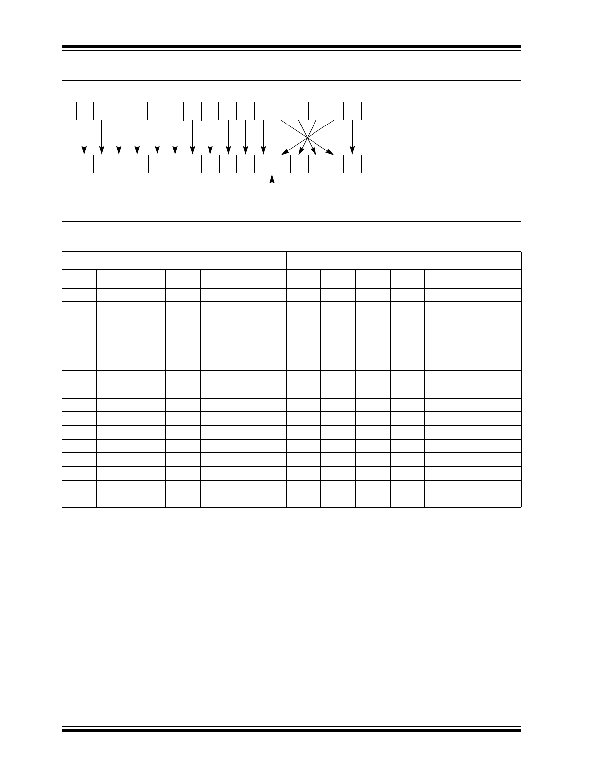
dsPIC33EVXXXGM00X/10X FAMILY
b3 b2 b1 0
b2
b3 b4 0
Bit Locations Swapped Left-to-Right
Around Center of Binary Value
Bit-Reversed Address
XB = 0x0008 for a 16-Word Bit-Reversed Buffer
b7 b6 b5 b1
b7
b6 b5 b4b11 b10 b9 b8
b11 b10 b9 b8
b15 b14 b13 b12
b15 b14 b13 b12
Sequential Address
Pivot Point
FIGURE 4-14: BIT-REVERSED ADDRESSING EXAMPLE
TABLE 4-46: BIT-REVERSED ADDRESSING SEQUENCE (16-ENTRY)
Normal Address Bit-Reversed Address
A3 A2 A1 A0 Decimal A3 A2 A1 A0 Decimal
0000 0 0000 0
0001 1 1000 8
0010 2 0100 4
0011 3 1100 12
0100 4 0010 2
0101 5 1010 10
0110 6 0110 6
0111 7 1110 14
1000 8 0001 1
1001 9 1001 9
1010 10 0101 5
1011 11 1101 13
1100 12 0011 3
1101 13 1011 11
1110 14 0111 7
1111 15 1111 15
DS70005144C-page 76 2013-2014 Microchip Technology Inc.
Page 77

dsPIC33EVXXXGM00X/10X FAMILY
4.7 Interfacing Program and Data
Memory Spaces
The dsPIC33EVXXXGM00X/10X family architecture
uses a 24-bit wide Program Space and a 16-bit wide
Data Space. The architecture is also a modified Harvard
scheme, meaning that data can also be present in the
Program Space. To use this data successfully, it must be
accessed in a way that preserves the alignment of
information in both the spaces.
Aside from normal execution, the architecture of the
dsPIC33EVXXXGM00X/10X family devices provides
two methods by which Program Space can be
accessed during operation:
• Using table instructions to access individual bytes
or words anywhere in the Program Space
• Remapping a portion of the Program Space into
the Data Space (Program Space Visibility)
Table instructions allow an application to read or write
to small areas of the program memory. This capability
makes the method ideal for accessing data tables that
need to be updated periodically. It also allows access
to all bytes of the program word. The remapping
method allows an application to access a large block of
data on a read-only basis, which is ideal for look-ups
from a large table of static data. The application can
only access the least significant word of the program
word.
Table 4-47 shows the construction of the Program
Space address.
How the data is accessed from Program Space is
shown in Figure 4-15.
TABLE 4-47: PROGRAM SPACE ADDRESS CONSTRUCTION
Access Type
Instruction Access
(Code Execution)
TBLRD/TBLWT
(Byte/Word Read/Write)
Access
Space
User 0 PC<22:1> 0
User TBLPAG<7:0> Data EA<15:0>
Configuration TBLPAG<7:0> Data EA<15:0>
<23> <22:16> <15> <14:1> <0>
0xx xxxx xxxx xxxx xxxx xxx0
0xxx xxxx xxxx xxxx xxxx xxxx
1xxx xxxx xxxx xxxx xxxx xxxx
Program Space Address
2013-2014 Microchip Technology Inc. DS70005144C-page 77
Page 78

dsPIC33EVXXXGM00X/10X FAMILY
0
Program Counter
23 Bits
Program Counter
(1)
TBLPAG
8 Bits
EA
16 Bits
Byte Select
0
1/0
User/Configuration
Table Operations
(2)
Space Select
24 Bits
1/0
Note 1: The Least Significant bit (LSb) of Program Space addresses is always fixed as ‘0’ to maintain word alignment
of data in the Program and Data Spaces.
2: Table operations are not required to be word-aligned. Table Read operations are permitted in the configuration
memory space.
FIGURE 4-15: DATA ACCESS FROM PROGRAM SPACE ADDRESS GENERATION
DS70005144C-page 78 2013-2014 Microchip Technology Inc.
Page 79

dsPIC33EVXXXGM00X/10X FAMILY
081623
00000000
00000000
00000000
00000000
‘Phantom’ Byte
TBLRDH.B (Wn<0> = 0)
TBLRDL.W
TBLRDL.B (Wn<0> = 1)
TBLRDL.B (Wn<0> = 0)
23 15 0
TBLPAG
02
0x000000
0x800000
0x020000
0x030000
Program Space
The address for the table operation is determined by the data EA
within the page defined by the TBLPAG register.
Only read operations are shown; write operations are also valid
in the user memory area.
4.7.1 DATA ACCESS FROM PROGRAM MEMORY USING TABLE INSTRUCTIONS
The TBLRDL and TBLWTL instructions offer a direct
method of reading or writing the lower word of any
address within the Program Space without going
through the Data Space. The TBLRDH and TBLWTH
instructions are the only method to read or write the
upper 8 bits of a Program Space word as data.
The PC is incremented by two for each successive
24-bit program word. This allows program memory
addresses to directly map to Data Space addresses.
Program memory can thus be regarded as two 16-bit
wide word address spaces, residing side by side, each
with the same address range. The TBLRDL and
TBLWTL instructions access the space that contains
the least significant data word and the upper data byte.
Two table instructions are provided to move byte or
word-sized (16-bit) data to and from Program Space.
Both function as either byte or word operations.
• TBLRDL (Table Read Low):
- In Word mode, this instruction maps the
lower word of the Program Space location
(P<15:0>) to a data address (D<15:0>).
- In Byte mode, either the upper or lower byte of
the lower program word is mapped to the lower
byte of a data address. The upper byte is
selected when Byte Select is ‘1’; the lower byte
is selected when it is ‘0’.
• TBLRDH (Table Read High):
- In Word mode, this instruction maps the entire
upper word of a program address (P<23:16>)
to a data address. The ‘phantom’ byte
(D<15:8>) is always ‘0’.
- In Byte mode, this instruction maps the upper
or lower byte of the program word to D<7:0>
of the data address in the TBLRDL instruc-
tion. The data is always ‘0’ when the upper
‘phantom’ byte is selected (Byte Select = 1).
Similarly, two table instructions, TBLWTH and TBLWTL,
are used to write individual bytes or words to a Program
Space address. The details of their operation are
explained in Section 5.0 “Flash Program Memory”.
For all table operations, the area of program memory
space to be accessed is determined by the Table Page
register (TBLPAG). TBLPAG covers the entire program
memory space of the device, including user application
and configuration spaces. When TBLPAG<7> = 0, the
table page is located in the user memory space. When
TBLPAG<7> = 1, the page is located in configuration
space. Accessing the program memory with table
instructions is shown in Figure 4-16.
FIGURE 4-16: ACCESSING PROGRAM MEMORY WITH TABLE INSTRUCTIONS
2013-2014 Microchip Technology Inc. DS70005144C-page 79
Page 80

dsPIC33EVXXXGM00X/10X FAMILY
NOTES:
DS70005144C-page 80 2013-2014 Microchip Technology Inc.
Page 81

dsPIC33EVXXXGM00X/10X FAMILY
0
Program Counter
24 Bits
Program Counter
TBLPAG Reg
8 Bits
Working Reg EA
16 Bits
Byte
24-Bit EA
0
1/0
Select
Using
Table Instruction
Using
User/Configuration
Space Select
5.0 FLASH PROGRAM MEMORY
Note 1: This data sheet summarizes the
features of the dsPIC33EVXXXGM00X/
10X family of devices. It is not intended
to be a comprehensive reference
source. To complement the information
in this data sheet, refer to “Flash Pro-
gramming” (DS70609) in the “dsPIC33/
PIC24 Family Reference Manual”, which
is available from the Microchip web site
(www.microchip.com).
2: Some registers and associated bits
described in this section may not be
available on all devices. Refer to
Section 4.0 “Memory Organization” in
this data sheet for device-specific register
and bit information.
The dsPIC33EVXXXGM00X/10X family devices
contain internal Flash program memory for storing and
executing application code. The memory is readable,
writable and erasable during normal operation over the
entire V
The Flash memory can be programmed in the following
three ways:
• In-Circuit Serial Programming™ (ICSP™)
• Run-Time Self-Programming (RTSP)
• Enhanced In-Circuit Serial Programming
ICSP allows for a dsPIC33EVXXXGM00X/10X family
device to be serially programmed while in the end
application circuit. This is done with two lines for
programming clock and programming data (PGECx/
PGEDx) lines, and three other lines for power (V
ground (V
customers to manufacture boards with unprogrammed
DD range.
(Enhanced ICSP)
DD),
SS) and Master Clear (MCLR). This allows
devices and then program the device just before
shipping the product. This also allows the most recent
firmware or a custom firmware to be programmed.
Enhanced ICSP uses an on-board bootloader, known as
the Program Executive (PE), to manage the programming
process. Using an SPI data frame format, the Program
Executive can erase, program and verify program
memory. For more information on Enhanced ICSP, refer
to the specific device programming specification.
RTSP is accomplished using the TBLRD (Table Read)
and TBLWT (Table Write) instructions. With RTSP, the
user application can write program memory data as a
double program memory word, a row of 64 instructions
(192 bytes) and erase program memory in blocks of
512 instruction words (1536 bytes) at a time.
5.1 Table Instructions and Flash
Programming
The Flash memory read and the double-word
programming operations make use of the TBLRD and
TBLWT instructions, respectively. These allow direct read
and write access to the program memory space from the
data memory while the device is in normal operating
mode. The 24-bit target address in the program memory
is formed using bits<7:0> of the TBLPAG register and
the Effective Address (EA) from a W register, specified
in the table instruction, as shown in Figure 5-1.
The TBLRDL and the TBLWTL instructions are used to
read or write to bits<15:0> of the program memory.
TBLRDL and TBLWTL can access program memory in
both Word and Byte modes.
The TBLRDH and TBLWTH instructions are used to read
or write to bits<23:16> of the program memory.
TBLRDH and TBLWTH can also access program
memory in Word or Byte mode.
FIGURE 5-1: ADDRESSING FOR TABLE REGISTERS
2013-2014 Microchip Technology Inc. DS70005144C-page 81
Page 82

dsPIC33EVXXXGM00X/10X FAMILY
LSW1
MSB10x00
LSW2
0x00 MSB2
LSW1
MSB1MSB2
LSW2
15 7 0
15 7 0
Even Byte
Address
Even Byte
Address
Increasing
Address
Increasing
Address
UNCOMPRESSED FORMAT (RPDF = 0)
COMPRESSED FORMAT (RPDF = 1)
5.2 RTSP Operation
RTSP allows the user application to erase a single
page of memory, program a row and to program two
instruction words at a time. See Ta ble 1 in the
“dsPIC33EVXXXGM00X/10X Product Families”
section for the page sizes of each device.
The Flash program memory array is organized into
rows of 64 instructions or 192 bytes. RTSP allows the
user application to erase a page of program memory,
which consists of eight rows (512 instructions) at a
time, and to program one row or two adjacent words at
a time. The 8-row erase pages and single row write
rows are edge-aligned, from the beginning of program
memory, on boundaries of 1536 bytes and 192 bytes,
respectively. Table 30-13 in Section 30.0 “Electrical
Characteristics” lists the typical erase and
programming times.
The basic sequence for RTSP word programming is to
use the TBLWTL and TBLWTH instructions to load two of
the 24-bit instructions into the write latches found in
configuration memory space. See Figure 4-1 to
Figure 4-4 for write latch addresses. Programming is
performed by unlocking and setting the control bits in
the NVMCON register.
Row programming is performed by loading 192 bytes
into data memory and then loading the address of the
first byte in that row into the NVMSRCADR register.
Once the write has been initiated, the device will automatically load the write latches and increment the
NVMSRCADR and the NVMADR(U) registers until all
bytes have been programmed. The RPDF bit
(NVMCON<9>) selects the format of the stored data in
RAM to be either compressed or uncompressed. See
Figure 5-2 for data formatting. Compressed data helps
to reduce the amount of required RAM by using the
upper byte of the second word for the MSB of the second
instruction.
For more information on erasing and programming the
Flash memory, refer to “Flash Programming”
(DS70609) in the “dsPIC33/PIC24 Family Reference
Manual”.
Note 1: Before reprogramming either of the two
2: Before reprogramming any word in a row,
words in a double-word pair, the user
must erase the Flash memory page in
which it is located.
the user must erase the Flash memory
page in which it is located.
FIGURE 5-2: UNCOMPRESSED/
COMPRESSED FORMAT
5.3 Programming Operations
A complete programming sequence is necessary for
programming or erasing the internal Flash in RTSP
mode. The processor stalls (waits) until the programming operation is finished. Setting the WR bit
(NVMCON<15>) starts the operation and the WR bit is
automatically cleared when the operation is finished.
5.3.1 PROGRAMMING ALGORITHM FOR FLASH PROGRAM MEMORY
Programmers can program two adjacent words
(24 bits x 2) of program Flash memory at a time on
every other word address boundary (0x000002,
0x000006, 0x00000A, etc.). To do this, erase the page
that contains the desired address of the location the
user wants to change. For protection against accidental
operations, the write initiate sequence for NVMKEY
must be used to allow any erase or program operation
to proceed. After the programming command has been
executed, the user application must wait for the programming time until programming is complete. The two
instructions following the start of the programming
sequence should be NOPs.
Refer to “Flash Programming” (DS70609) in the
“dsPIC33/PIC24 Family Reference Manual” for details
and code examples on programming using RTSP.
DS70005144C-page 82 2013-2014 Microchip Technology Inc.
Page 83

dsPIC33EVXXXGM00X/10X FAMILY
5.4 Error Correcting Code (ECC)
In order to improve program memory performance and
durability, these devices include Error Correcting Code
functionality (ECC) as an integral part of the Flash
memory controller. ECC can determine the presence of
single-bit errors in program data, including which bit is
in error, and correct the data automatically without user
intervention. ECC cannot be disabled.
When data is written to program memory, ECC
generates a 7-bit Hamming code parity value for every
two (24-bit) instruction words. The data is stored in
blocks of 48 data bits and 7 parity bits; parity data is not
memory-mapped and is inaccessible. When the data is
read back, the ECC calculates the parity on it and
compares it to the previously stored parity value. If a
parity mismatch occurs, there are two possible
outcomes:
• Single-bit errors are automatically identified and
corrected on read-back. An optional device-level
interrupt (ECCSBEIF) is also generated.
• Double-bit errors will generate a generic hard trap
and the read data is not changed. If special
exception handling for the trap is not
implemented, a device Reset will also occur.
To use the single-bit error interrupt, set the ECC SingleBit Error Interrupt Enable bit (ECCSBEIE) and
configure the ECCSBEIP bits to set the appropriate
interrupt priority.
Except for the single-bit error interrupt, error events are
not captured or counted by hardware. This functionality
can be implemented in the software application, but it
is the user’s responsibility to do so.
5.5 Flash Memory Resources
Many useful resources are provided on the main
product page of the Microchip web site for the devices
listed in this data sheet. This product page contains the
latest updates and additional information.
5.5.1 KEY RESOURCES
• Code Samples
• Application Notes
• Software Libraries
• Webinars
• All Related “dsPIC33/PIC24 Family Reference
Manual” Sections
• Development Tools
5.6 Control Registers
The following five SFRs are used to read and write the
program Flash memory: NVMCON, NVMKEY,
NVMADR, NVMADRU and NVMSRCADR.
The NVMCON register (Register 5-1) selects the
operation to be performed (page erase, word/row
program, inactive panel erase) and initiates the
program/erase cycle.
NVMKEY (Register 5-4) is a write-only register that is
used for write protection. To start a programming or
erase sequence, the user application must
consecutively write 0x55 and 0xAA to the NVMKEY
register.
There are two NVM Address registers: NVMADRU and
NVMADR. These two registers, when concatenated,
form the 24-bit Effective Address (EA) of the selected
word/row for programming operations or the selected
page for erase operations. The NVMADRU register is
used to hold the upper 8 bits of the EA, while the
NVMADR register is used to hold the lower 16 bits of
the EA. For row programming operation, data to be
written to program Flash memory is written into data
memory space (RAM) at an address defined by the
NVMSRCADR register (location of the first element in
row programming data).
2013-2014 Microchip Technology Inc. DS70005144C-page 83
Page 84

dsPIC33EVXXXGM00X/10X FAMILY
REGISTER 5-1: NVMCON: NONVOLATILE MEMORY (NVM) CONTROL REGISTER
R/SO-0 R/W-0 R/W-0 R/W-0 U-0 U-0 R/W-0 R/W-0
(1)
WR
bit 15 bit 8
U-0 U-0 U-0 U-0 R/W-0 R/W-0 R/W-0 R/W-0
— — — —NVMOP3
bit 7 bit 0
Legend: SO = Settable Only bit
R = Readable bit W = Writable bit U = Unimplemented bit, read as ‘0’
-n = Value at POR ‘1’ = Bit is set ‘0’ = Bit is cleared x = Bit is unknown
WREN
(1)
WRERR
(1)
NVMSIDL
(2)
— — RPDF URERR
(1,3,4)
NVMOP2
(1,3,4)
NVMOP1
(1,3,4)
NVMOP0
(1,3,4)
bit 15 WR: Write Control bit
(1)
1 = Initiates a Flash memory program or erase operation; the operation is self-timed and the bit is
cleared by hardware once the operation is complete
0 = Program or erase operation is complete and inactive
bit 14 WREN: Write Enable bit
(1)
1 = Flash program or erase operations are enabled
0 = Flash program or erase operations are inhibited
bit 13 WRERR: Write Sequence Error Flag bit
(1)
1 = An improper program or erase sequence attempt, or termination has occurred (bit is set automatically
on any set attempt of the WR bit)
0 = The program or erase operation completed normally
bit 12 NVMSIDL: NVM Stop in Idle Control bit
(2)
1 = Primary Flash operation discontinues when the device enters Idle mode
0 = Primary Flash operation continues when the device enters Idle mode.
bit 11-10 Unimplemented: Read as ‘0’
bit 9 RPDF: Row Programming Data Format Control bit
1 = Row data to be stored in RAM is in a compressed format
0 = Row data to be stored in RAM is in an uncompressed format
bit 8 URERR: Row Programming Data Underrun Error Flag bit
1 = Row programming operation has been terminated due to a data underrun error
0 = No data underrun has occurred
bit 7-4 Unimplemented: Read as ‘0’
Note 1: These bits can only be reset on a POR.
2: If this bit is set, there will be minimal power savings (I
VREG) before Flash memory becomes operational.
(T
IDLE), and upon exiting Idle mode, there is a delay
3: All other combinations of NVMOP<3:0> are unimplemented.
4: Execution of the PWRSAV instruction is ignored while any of the NVM operations are in progress.
5: Two adjacent words on a 4-word boundary are programmed during execution of this operation.
DS70005144C-page 84 2013-2014 Microchip Technology Inc.
Page 85

dsPIC33EVXXXGM00X/10X FAMILY
REGISTER 5-1: NVMCON: NONVOLATILE MEMORY (NVM) CONTROL REGISTER (CONTINUED)
bit 3-0 NVMOP<3:0>: NVM Operation Select bits
1111 = Reserved
1110 = User memory and executive memory bulk erase operation
1101 = Reserved
1100 = Reserved
1011 = Reserved
1010 = Reserved
1001 = Reserved
1000 = Reserved
0111 = Reserved
0101 = Reserved
0100 = Reserved
0011 = Memory page erase operation
0010 = Memory row program operation
0001 = Memory double-word
0000 = Reserved
Note 1: These bits can only be reset on a POR.
2: If this bit is set, there will be minimal power savings (IIDLE), and upon exiting Idle mode, there is a delay
VREG) before Flash memory becomes operational.
(T
3: All other combinations of NVMOP<3:0> are unimplemented.
4: Execution of the PWRSAV instruction is ignored while any of the NVM operations are in progress.
5: Two adjacent words on a 4-word boundary are programmed during execution of this operation.
(5)
(1,3,4)
REGISTER 5-2: NVMADRU: NONVOLATILE MEMORY UPPER ADDRESS REGISTER
U-0 U-0 U-0 U-0 U-0 U-0 U-0 U-0
— — — — — — — —
bit 15 bit 8
R/W-x R/W-x R/W-x R/W-x R/W-x R/W-x R/W-x R/W-x
NVMADRU<23:16>
bit 7 bit 0
Legend:
R = Readable bit W = Writable bit U = Unimplemented bit, read as ‘0’
-n = Value at POR ‘1’ = Bit is set ‘0’ = Bit is cleared x = Bit is unknown
bit 15-8 Unimplemented: Read as ‘0’
bit 7-0 NVMADRU<23:16>: NVM Memory Upper Write Address bits
Selects the upper 8 bits of the location to program or erase in program Flash memory. This register may be
read or written to by the user application.
2013-2014 Microchip Technology Inc. DS70005144C-page 85
Page 86

dsPIC33EVXXXGM00X/10X FAMILY
REGISTER 5-3: NVMADR: NONVOLATILE MEMORY LOWER ADDRESS REGISTER
R/W-x R/W-x R/W-x R/W-x R/W-x R/W-x R/W-x R/W-x
NVMADR<15:8>
bit 15 bit 8
R/W-x R/W-x R/W-x R/W-x R/W-x R/W-x R/W-x R/W-x
NVMADR<7:0>
bit 7 bit 0
Legend:
R = Readable bit W = Writable bit U = Unimplemented bit, read as ‘0’
-n = Value at POR ‘1’ = Bit is set ‘0’ = Bit is cleared x = Bit is unknown
bit 15-0 NVMADR<15:0>: NVM Memory Lower Write Address bits
Selects the lower 16 bits of the location to program or erase in program Flash memory. This register
may be read or written to by the user application.
REGISTER 5-4: NVMKEY: NONVOLATILE MEMORY KEY REGISTER
U-0 U-0 U-0 U-0 U-0 U-0 U-0 U-0
— — — — — — — —
bit 15 bit 8
W-0 W-0 W-0 W-0 W-0 W-0 W-0 W-0
NVMKEY<7:0>
bit 7 bit 0
Legend:
R = Readable bit W = Writable bit U = Unimplemented bit, read as ‘0’
-n = Value at POR ‘1’ = Bit is set ‘0’ = Bit is cleared x = Bit is unknown
bit 15-8 Unimplemented: Read as ‘0’
bit 7-0 NVMKEY<7:0>: NVM Key Register bits (write-only)
DS70005144C-page 86 2013-2014 Microchip Technology Inc.
Page 87

dsPIC33EVXXXGM00X/10X FAMILY
REGISTER 5-5: NVMSRCADRH: NVM DATA MEMORY UPPER ADDRESS REGISTER
U-0 U-0 U-0 U-0 U-0 U-0 U-0 U-0
— — — — — — — —
bit 15 bit 8
R/W-x R/W-x R/W-x R/W-x R/W-x R/W-x R/W-x R/W-x
NVMSRCADR<23:16>
bit 7 bit 0
Legend:
R = Readable bit W = Writable bit U = Unimplemented bit, read as ‘0’
-n = Value at POR ‘1’ = Bit is set ‘0’ = Bit is cleared x = Bit is unknown
bit 15-8 Unimplemented: Read as ‘0’
bit 7-0 NVMSRCADRH<23:16>: Data Memory Upper Address bits
REGISTER 5-6: NVMSRCADRL: NVM DATA MEMORY LOWER ADDRESS REGISTER
R/W-x R/W-x R/W-x R/W-x R/W-x R/W-x R/W-x R/W-x
NVMSRCADR<15:8>
bit 15 bit 8
R/W-x R/W-x R/W-x R/W-x R/W-x R/W-x R/W-x r-0
NVMSRCADR<7:1>
bit 7 bit 0
Legend: r = Reserved bit
R = Readable bit W = Writable bit U = Unimplemented bit, read as ‘0’
-n = Value at POR ‘1’ = Bit is set ‘0’ = Bit is cleared x = Bit is unknown
bit 15-1 NVMSRCADRL<15:1>: Data Memory Lower Address bits
bit 0 Reserved: Maintain as ‘0’
r
2013-2014 Microchip Technology Inc. DS70005144C-page 87
Page 88

dsPIC33EVXXXGM00X/10X FAMILY
NOTES:
DS70005144C-page 88 2013-2014 Microchip Technology Inc.
Page 89

dsPIC33EVXXXGM00X/10X FAMILY
6.0 RESETS
Note 1: This data sheet summarizes the features
of the dsPIC33EVXXXGM00X/10X family
of devices. It is not intended to be a
comprehensive reference source. To complement the information in this data sheet,
refer to “Reset” (DS70602) in the
“dsPIC33/PIC24 Family Reference Manual”, which is available from the Microchip
web site (www.microchip.com).
2: Some registers and associated bits
described in this section may not be
available on all devices. Refer to
Section 4.0 “Memory Organization” in
this data sheet for device-specific register
and bit information.
The Reset module combines all Reset sources and
controls the device Master Reset Signal, SYSRST
following is a list of device Reset sources:
• POR: Power-on Reset
• BOR: Brown-out Reset
•MCLR
•SWR: RESET Instruction
• WDTO: Watchdog Timer Time-out Reset
• CM: Configuration Mismatch Reset
• TRAPR: Trap Conflict Reset
• IOPUWR: Illegal Condition Device Reset
: Master Clear Pin Reset
- Illegal Opcode Reset
- Uninitialized W Register Reset
- Security Reset
- Illegal Address Mode Reset
. The
A simplified block diagram of the Reset module is
shown in Figure 6-1.
Any active source of Reset will make the SYSRST
signal active. On system Reset, some of the registers
associated with the CPU and peripherals are forced to
a known Reset state and some are unaffected.
Note: Refer to the specific peripheral section or
Section 4.0 “Memory Organization” of
this device data sheet for register Reset
states.
All types of device Reset set a corresponding status bit
in the RCON register to indicate the type of Reset (see
Register 6-1).
A POR clears all the bits, except for the POR and BOR
bits (RCON<1:0>) that are set. The user application
can set or clear any bit at any time during code
execution. The RCON bits only serve as status bits.
Setting a particular Reset status bit in software does
not cause a device Reset to occur.
The RCON register also has other bits associated with
the Watchdog Timer and device power-saving states.
The function of these bits is discussed in the other
sections of this device data sheet.
Note: The status bits in the RCON register
should be cleared after they are read.
Therefore, the next RCON register value
after a device Reset is meaningful.
Note: In all types of Resets, to select the device
clock source, the contents of OSCCON are
initialized from the FNOSCx Configuration
bits in the FOSCSEL Configuration register.
2013-2014 Microchip Technology Inc. DS70005144C-page 89
Page 90

dsPIC33EVXXXGM00X/10X FAMILY
MCLR
VDD
BOR
Sleep or Idle
RESET Instruction
WDT
Module
Glitch Filter
Trap Conflict
Illegal Opcode
Uninitialized W Register
SYSRST
POR
Configuration Mismatch
Security Reset
Internal
Regulator
Illegal Address Mode Reset
VDD Rise
Detect
FIGURE 6-1: RESET SYSTEM BLOCK DIAGRAM
DS70005144C-page 90 2013-2014 Microchip Technology Inc.
Page 91

dsPIC33EVXXXGM00X/10X FAMILY
REGISTER 6-1: RCON: RESET CONTROL REGISTER
(1)
R/W-0 R/W-0 U-0 U-0 R/W-0 U-0 R/W-0 R/W-0
TRAPR IOPUWR
— —VREGSF —CMVREGS
bit 15 bit 8
R/W-0 R/W-0 R/W-0 R/W-0 R/W-0 R/W-0 R/W-1 R/W-1
(2)
EXTR SWR SWDTEN
WDTO SLEEP IDLE BOR POR
bit 7 bit 0
Legend:
R = Readable bit W = Writable bit U = Unimplemented bit, read as ‘0’
-n = Value at POR ‘1’ = Bit is set ‘0’ = Bit is cleared x = Bit is unknown
bit 15 TRAPR: Trap Reset Flag bit
1 = A Trap Conflict Reset has occurred
0 = A Trap Conflict Reset has not occurred
bit 14 IOPUWR: Illegal Opcode or Uninitialized W Register Access Reset Flag bit
1 = An Illegal Opcode Reset detection or an Illegal Address mode, or Uninitialized W register used as
an Address Pointer caused a Reset
0 = An Illegal Opcode Reset or Uninitialized W Register Reset has not occurred
bit 13-12 Unimplemented: Read as ‘0’
bit 11 VREGSF: Flash Voltage Regulator Standby During Sleep bit
1 = Flash voltage regulator is active during Sleep mode
0 = Flash voltage regulator goes into Standby mode during Sleep mode
bit 10 Unimplemented: Read as ‘0’
bit 9 CM: Configuration Mismatch Flag bit
1 = A Configuration Mismatch Reset has occurred.
0 = A Configuration Mismatch Reset has not occurred
bit 8 VREGS: Voltage Regulator Standby During Sleep bit
1 = Voltage regulator is active during Sleep
0 = Voltage regulator goes into Standby mode during Sleep
bit 7 EXTR: External Reset (MCLR
) Pin bit
1 = A Master Clear (pin) Reset has occurred
0 = A Master Clear (pin) Reset has not occurred
bit 6 SWR: Software RESET (Instruction) Flag bit
1 = A RESET instruction has been executed
0 = A RESET instruction has not been executed
bit 5 SWDTEN: Software Enable/Disable of WDT bit
(2)
1 = WDT is enabled
0 = WDT is disabled
bit 4 WDTO: Watchdog Timer Time-out Flag bit
1 = WDT time-out has occurred
0 = WDT time-out has not occurred
Note 1: All of the Reset status bits can be set or cleared in software. Setting one of these bits in software does not
cause a device Reset.
2: If the FWDTEN<1:0> Configuration bits are ‘11’ (unprogrammed), the WDT is always enabled, regardless
of the SWDTEN bit setting.
2013-2014 Microchip Technology Inc. DS70005144C-page 91
Page 92

dsPIC33EVXXXGM00X/10X FAMILY
REGISTER 6-1: RCON: RESET CONTROL REGISTER
bit 3 SLEEP: Wake-up from Sleep Flag bit
1 = Device has been in Sleep mode
0 = Device has not been in Sleep mode
bit 2 IDLE: Wake-up from Idle Flag bit
1 = Device was in Idle mode
0 = Device was not in Idle mode
bit 1 BOR: Brown-out Reset Flag bit
1 = A Brown-out Reset has occurred
0 = A Brown-out Reset has not occurred
bit 0 POR: Power-on Reset Flag bit
1 = A Power-on Reset has occurred
0 = A Power-on Reset has not occurred
Note 1: All of the Reset status bits can be set or cleared in software. Setting one of these bits in software does not
cause a device Reset.
2: If the FWDTEN<1:0> Configuration bits are ‘11’ (unprogrammed), the WDT is always enabled, regardless
of the SWDTEN bit setting.
(1)
(CONTINUED)
DS70005144C-page 92 2013-2014 Microchip Technology Inc.
Page 93

dsPIC33EVXXXGM00X/10X FAMILY
7.0 INTERRUPT CONTROLLER
Note 1: This data sheet summarizes the features
of the dsPIC33EVXXXGM00X/10X
family of devices. It is not intended to be
a comprehensive reference source. To
complement the information in this
data sheet, refer to “Interrupts”
(DS70000600) in the “dsPIC33/PIC24
Family Reference Manual”, which is
available from the Microchip web site
(www.microchip.com).
2: Some registers and associated bits
described in this section may not be
available on all devices. Refer to
Section 4.0 “Memory Organization” in
this data sheet for device-specific register
and bit information.
The dsPIC33EVXXXGM00X/10X family interrupt controller reduces the numerous peripheral interrupt
request signals to a single interrupt request signal to
the dsPIC33EVXXXGM00X/10X CPU. The Interrupt
Vector Table (IVT) provides 246 interrupt sources
(unused sources are reserved for future use) that can
be programmed with different priority levels.
The interrupt controller has the following features:
• Interrupt Vector Table with up to 246 Vectors
• Alternate Interrupt Vector Table (AIVT)
• Up to Eight Processor Exceptions and Software
Traps
• Seven User-Selectable Priority Levels
• Interrupt Vector Table (IVT) with a Unique Vector
for Each Interrupt or Exception Source
• Fixed Priority within a Specified User Priority Level
• Fixed Interrupt Entry and Return Latencies
• Software can Generate any Peripheral Interrupt
• Alternate Interrupt Vector Table (AIVT) if Boot
Security is Enabled and AIVTEN = 1
7.1 Interrupt Vector Table
The dsPIC33EVXXXGM00X/10X family IVT, shown
in Figure 7-2, resides in program memory, starting at
location, 000004h. The IVT contains seven nonmaskable trap vectors and up to 187 sources of
interrupt. In general, each interrupt source has its own
vector. Each interrupt vector contains a 24-bit wide
address. The value programmed into each interrupt
vector location is the starting address of the associated
Interrupt Service Routine (ISR).
Interrupt vectors are prioritized in terms of their natural
priority. This priority is linked to their position in the
vector table. Lower addresses generally have a higher
natural priority. For example, the interrupt associated
with Vector 0 takes priority over interrupts at any other
vector address.
7.2 Alternate Interrupt Vector Table
The Alternate Interrupt Vector Table (AIVT), shown in
Figure 7-1, is available if the Boot Segment (BS) is
defined, the AIVTEN bit is set in the INTCON2 register
and if the AIVTDIS Configuration bit is set to ‘1’. The
AIVT begins at the start of the last page of the Boot
Segment.
2013-2014 Microchip Technology Inc. DS70005144C-page 93
Page 94

dsPIC33EVXXXGM00X/10X FAMILY
IVT
Reserved BSLIM<12:0>
(1)
+ 0x000000
Reserved BSLIM<12:0>
(1)
+ 0x000002
Oscillator Fail Trap Vector BSLIM<12:0>
(1)
+ 0x000004
Address Error Trap Vector BSLIM<12:0>
(1)
+ 0x000006
Generic Hard Trap Vector BSLIM<12:0>
(1)
+ 0x000008
Stack Error Trap Vector BSLIM<12:0>
(1)
+ 0x00000A
Math Error Trap Vector BSLIM<12:0>
(1)
+ 0x00000C
DMAC Error Trap Vector BSLIM<12:0>
(1)
+ 0x00000E
Generic Soft Trap Vector BSLIM<12:0>
(1)
+ 0x000010
Reserved BSLIM<12:0>
(1)
+ 0x000012
Interrupt Vector 0 BSLIM<12:0>
(1)
+ 0x000014
Interrupt Vector 1 BSLIM<12:0>
(1)
+ 0x000016
::
::
::
Interrupt Vector 52 BSLIM<12:0>
(1)
+ 0x00007C
Interrupt Vector 53 BSLIM<12:0>
(1)
+ 0x00007E
Interrupt Vector 54 BSLIM<12:0>
(1)
+ 0x000080
::
::
::
Interrupt Vector 116 BSLIM<12:0>
(1)
+ 0x0000FC
Interrupt Vector 117 BSLIM<12:0>
(1)
+ 0x00007E
Interrupt Vector 118 BSLIM<12:0>
(1)
+ 0x000100
Interrupt Vector 119 BSLIM<12:0>
(1)
+ 0x000102
Interrupt Vector 120 BSLIM<12:0>
(1)
+ 0x000104
::
::
::
Interrupt Vector 244 BSLIM<12:0>
(1)
+ 0x0001FC
Interrupt Vector 245 BSLIM<12:0>
(1)
+ 0x0001FE
See Table 7-1 for
Interrupt Vector Details
Note 1: The address depends on the size of the Boot Segment defined by BSLIM<12:0>:
[(BSLIM<12:0> – 1) x 0x400] + Offset.
FIGURE 7-1: dsPIC33EVXXXGM00X/10X FAMILY ALTERNATE INTERRUPT VECTOR TABLE
DS70005144C-page 94 2013-2014 Microchip Technology Inc.
Page 95

dsPIC33EVXXXGM00X/10X FAMILY
IVT
Decreasing Natural Order Priority
Reset – GOTO Instruction 0x000000
Reset – GOTO Address 0x000002
Oscillator Fail Trap Vector 0x000004
Address Error Trap Vector 0x000006
Generic Hard Trap Vector 0x000008
Stack Error Trap Vector 0x00000A
Math Error Trap Vector 0x00000C
DMAC Error Trap Vector 0x00000E
Generic Soft Trap Vector 0x000010
Reserved 0x000012
Interrupt Vector 0 0x000014
Interrupt Vector 1 0x000016
::
::
::
Interrupt Vector 52 0x00007C
Interrupt Vector 53 0x00007E
Interrupt Vector 54 0x000080
::
::
::
Interrupt Vector 116 0x0000FC
Interrupt Vector 117 0x0000FE
Interrupt Vector 118 0x000100
Interrupt Vector 119 0x000102
Interrupt Vector 120 0x000104
::
::
::
Interrupt Vector 244 0x0001FC
Interrupt Vector 245 0x0001FE
START OF CODE 0x000200
See Tab le 7 -1 for
Interrupt Vector Details
FIGURE 7-2: dsPIC33EVXXXGM00X/10X FAMILY INTERRUPT VECTOR TABLE
2013-2014 Microchip Technology Inc. DS70005144C-page 95
Page 96

dsPIC33EVXXXGM00X/10X FAMILY
TABLE 7-1: INTERRUPT VECTOR DETAILS
Interrupt Source
External Interrupt 0 (INT0) 8 0 0x000014 IFS0<0> IEC0<0> IPC0<2:0>
Input Capture 1 (IC1) 9 1 0x000016 IFS0<1> IEC0<1> IPC0<6:4>
Output Compare 1 (OC1) 10 2 0x000018 IFS0<2> IEC0<2> IPC0<10:8>
Timer1 (T1) 11 3 0x00001A IFS0<3> IEC0<3> IPC0<14:12>
DMA Channel 0 (DMA0) 12 4 0x00001C IFS0<4> IEC0<4> IPC1<2:0>
Input Capture 2 (IC2) 13 5 0x00001E IFS0<5> IEC0<5> IPC1<6:4>
Output Compare 2 (OC2) 14 6 0x000020 IFS0<6> IEC0<6> IPC1<10:8>
Timer2 (T2) 15 7 0x000022 IFS0<7> IEC0<7> IPC1<14:12>
Timer3 (T3) 16 8 0x000024 IFS0<8> IEC0<8> IPC2<2:0>
SPI1 Error (SPI1E) 17 9 0x000026 IFS0<9> IEC0<9> IPC2<6:4>
SPI1 Transfer Done (SPI1) 18 10 0x000028 IFS0<10> IEC0<10> IPC2<10:8>
UART1 Receiver (U1RX) 19 11 0x00002A IFS0<11> IEC0<11> IPC2<14:12>
UART1 Transmitter (U1TX) 20 12 0x00002C IFS0<12> IEC0<12> IPC3<2:0>
ADC1 Convert Done (AD1) 21 13 0x00002E IFS0<13> IEC0<13> IPC3<6:4>
DMA Channel 1 (DMA1) 22 14 0x000030 IFS0<14> IEC0<14> IPC3<10:8>
NVM Write Complete (NVM) 23 15 0x000032 IFS0<15> IEC0<15> IPC3<14:12>
I2C1 Slave Event (SI2C1) 24 16 0x000034 IFS1<0> IEC1<0> IPC4<2:0>
I2C1 Master Event (MI2C1) 25 17 0x000036 IFS1<1> IEC1<1> IPC4<6:4>
Comparator Combined Event
(CMP1)
Input Change Interrupt (CN) 27 19 0x00003A IFS1<3> IEC1<3> IPC4<14:12>
External Interrupt 1 (INT1) 28 20 0x00003C IFS1<4> IEC1<4> IPC5<2:0>
DMA Channel 2 (DMA2) 32 24 0x000044 IFS1<8> IEC1<8> IPC6<2:0>
Output Compare 3 (OC3) 33 25 0x000046 IFS1<9> IEC1<9> IPC6<6:4>
Output Compare 4 (OC4) 34 26 0x000048 IFS1<10> IEC1<10> IPC6<10:8>
Timer4 (T4) 35 27 0x00004A IFS1<11> IEC1<11> IPC6<14:12>
Timer5 (T5) 36 28 0x00004C IFS1<12> IEC1<12> IPC7<2:0>
External Interrupt 2 (INT2) 37 29 0x00004E IFS1<13> IEC1<13> IPC7<6:4>
UART2 Receiver (U2RX) 38 30 0x000050 IFS1<14> IEC1<14> IPC7<10:8>
UART2 Transmitter (U2TX) 39 31 0x000052 IFS1<15> IEC1<15> IPC7<14:12>
SPI2 Error (SPI2E) 40 32 0x000054 IFS2<0> IEC2<0> IPC8<2:0>
SPI2 Transfer Done (SPI2) 41 33 0x000056 IFS2<1> IEC2<1> IPC8<6:4>
CAN1 RX Data Ready
CAN1 Event (C1)
DMA Channel 3 (DMA3) 44 36 0x00005C IFS2<4> IEC2<4> IPC9<2:0>
Input Capture 3 (IC3) 45 37 0x00005E IFS2<5> IEC2<5> IPC9<6:4>
Input Capture 4 (IC4) 46 38 0x000060 IFS2<6> IEC2<6> IPC9<10:8>
Reserved 54 46 0x000070 — — —
PWM Special Event Match
Interrupt (PSEM)
Reserved 69 61 0x00008E — — —
Reserved 71-72 63-64 0x000092-0x000094 — — —
Note 1: This interrupt source is available on dsPIC33EVXXXGM10X devices only.
(C1RX)
(1)
Vec tor
No.
26 18 0x000038 IFS1<2> IEC1<2> IPC4<10:8>
(1)
42 34 0x000058 IFS2<2> IEC2<2> IPC8<10:8>
43 35 0x00005A IFS2<3> IEC2<3> IPC8<14:12>
65 57 0x000086 IFS3<9> IEC3<9> IPC14<6:4>
IRQ
No.
Highest Natural Order Priority
IVT Address
Interrupt Bit Location
Flag Enable Priority
DS70005144C-page 96 2013-2014 Microchip Technology Inc.
Page 97

dsPIC33EVXXXGM00X/10X FAMILY
TABLE 7-1: INTERRUPT VECTOR DETAILS (CONTINUED)
Interrupt Source
UART1 Error Interrupt (U1E) 73 65 0x000096 IFS4<1> IEC4<1> IPC16<6:4>
UART2 Error Interrupt (U2E) 74 66 0x000098 IFS4<2> IEC4<2> IPC16<10:8>
Reserved 76-77 68–69 0x00009C-0x00009E — — —
CAN1 TX Data Request (C1TX)
Reserved 80 72 0x0000A4 — — —
Reserved 82 74 0x0000A8 — — —
Reserved 84 76 0x0000AC — — —
CTMU Interrupt (CTMU) 85 77 0x0000AE IFS4<13> IEC4<13> IPC19<6:4>
Reserved 86-88 78-80 0x0000B0-0x0000B4 — — —
Reserved 92-94 84-86 0x0000BC-0x0000C0 — — —
Reserved 100-101 92-93 0x0000CC-0x0000CE — — —
PWM Generator 1 (PWM1) 102 94 0x0000D0 IFS5<14> IEC5<14> IPC23<10:8>
PWM Generator 2 (PWM2) 103 95 0x0000D2 IFS5<15> IEC5<15> IPC23<14:12>
PWM Generator 3 (PWM3) 104 96 0x0000D4 IFS6<0> IEC6<0> IPC24<2:0>
Reserved 108-149 100-141 0x0000DC-0x00012E — — —
ICD Application (ICD) 150 142 0x000142 IFS8<14> IEC8<14> IPC35<10:8>
Reserved 152 144 0x000134 — — —
Bus Collision (I2C1) — 173 0x00016E IFS10<13> IEC10<13> IPC43<4:6>
SENT1 Error (SENT1ERR) — 182 0x000180 IFS11<6> IEC11<6> IPC45<10:8>
SENT1 TX/RX (SENT1) — 183 0x000182 IFS11<7> IEC11<7> IPC45<14:12>
SENT2 Error (SENT2ERR) — 184 0x000184 IFS11<8> IEC11<8> IPC46<2:0>
SENT2 TX/RX (SENT2) — 185 0x000186 IFS11<9> IEC11<9> IPC46<6:4>
ECC Single Bit Error (ECCSBE) — 186 0x000188 IFS11<10> IEC11<10> IPC45<10:8>
Reserved 159-245 187-245 0x000142-0x0001FE — — —
Note 1: This interrupt source is available on dsPIC33EVXXXGM10X devices only.
Vec tor
No.
(1)
78 70 0x0000A0 IFS4<6> IEC4<6> IPC17<10:8>
IRQ
No.
Lowest Natural Order Priority
IVT Address
Interrupt Bit Location
Flag Enable Priority
2013-2014 Microchip Technology Inc. DS70005144C-page 97
Page 98

dsPIC33EVXXXGM00X/10X FAMILY
7.3 Reset Sequence
A device Reset is not a true exception because the
interrupt controller is not involved in the Reset process.
The dsPIC33EVXXXGM00X/10X family devices clear
their registers in response to a Reset, which forces the
PC to zero. The device then begins program execution
at location, 0x000000. A GOTO instruction at the Reset
address can redirect program execution to the
appropriate start-up routine.
Note: Any unimplemented or unused vector
locations in the IVT should be programmed with the address of a default
interrupt handler routine that contains a
RESET instruction.
7.4 Interrupt Control and Status Registers
dsPIC33EVXXXGM00X/10X family devices implement
the following registers for the interrupt controller:
• INTCON1
• INTCON2
• INTCON3
• INTCON4
•IFSx
•IECx
•IPCx
•INTTREG
7.4.1 INTCON1 THROUGH INTCON4
Global interrupt control functions are controlled from
the INTCON1, INTCON2, INTCON3 and INTCON4
registers.
INTCON1 contains the Interrupt Nesting Disable bit
(NSTDIS), as well as the control and status flags for the
processor trap sources.
The INTCON2 register controls external interrupt
request signal behavior and also contains the Global
Interrupt Enable bit (GIE).
INTCON3 contains the status flags for the DMT (Deadman Timer), DMA and DO stack overflow status trap
sources.
The INTCON4 register contains the ECC Double-Bit
Error (ECCDBE) and Software Generated Hard Trap
(SGHT) status bit.
7.4.3 IECx
The IECx registers maintain all of the interrupt enable
bits. These control bits are used to individually enable
interrupts from the peripherals or external signals.
7.4.4 IPCx
The IPCx registers are used to set the Interrupt Priority
Level (IPL) for each source of interrupt. Each user
interrupt source can be assigned to one of eight priority
levels.
7.4.5 INTTREG
The INTTREG register contains the associated
interrupt vector number and the new CPU Interrupt
Priority Level, which are latched into Vector Number
(VECNUM<7:0>) and Interrupt Priority Level bit
(ILR<3:0>) fields in the INTTREG register. The new
Interrupt Priority Level is the priority of the pending
interrupt.
The interrupt sources are assigned to the IFSx, IECx
and IPCx registers in the same sequence as they are
listed in Table 7-1. For example, the INT0 (External
Interrupt 0) is shown as having Vector Number 8 and a
natural order priority of 0. Thus, the INT0IF bit is found
in IFS0<0>, the INT0IE bit in IEC0<0> and the INT0IP
bits in the first position of IPC0 (IPC0<2:0>).
7.4.6 STATUS/CONTROL REGISTERS
Although these registers are not specifically part of the
interrupt control hardware, two of the CPU Control
registers contain bits that control interrupt functionality.
For more information on these registers, refer to
“CPU” (DS70359) in the “dsPIC33/PIC24 Family
Reference Manual”.
• The CPU STATUS Register, SR, contains the
IPL<2:0> bits (SR<7:5>). These bits indicate the
current CPU Interrupt Priority Level. The user
software can change the current CPU Interrupt
Priority Level by writing to the IPLx bits.
• The CORCON register contains the IPL3 bit
which, together with IPL<2:0>, also indicates the
current CPU Interrupt Priority Level. IPL3 is a
read-only bit so that trap events cannot be
masked by the user software.
All Interrupt registers are described in Register 7-3 to
Register 7-7.
7.4.2 IFSx
The IFSx registers maintain all of the interrupt request
flags. Each source of interrupt has a status bit, which is
set by the respective peripherals or external signal and
is cleared through software.
DS70005144C-page 98 2013-2014 Microchip Technology Inc.
Page 99

dsPIC33EVXXXGM00X/10X FAMILY
REGISTER 7-1: SR: CPU STATUS REGISTER
R/W-0 R/W-0 R/W-0 R/W-0 R/C-0 R/C-0 R-0 R/W-0
OA OB SA SB OAB SAB DA DC
bit 15 bit 8
R/W-0 R/W-0 R/W-0 R-0 R/W-0 R/W-0 R/W-0 R/W-0
(2,3)
IPL2
bit 7 bit 0
Legend: C = Clearable bit
R = Readable bit W = Writable bit U = Unimplemented bit, read as ‘0’
-n = Value at POR ‘1’ = Bit is set ‘0’ = Bit is cleared x = Bit is unknown
bit 7-5 IPL<2:0>: CPU Interrupt Priority Level Status bits
(2,3)
IPL1
111 = CPU Interrupt Priority Level is 7 (15); user interrupts are disabled
110 = CPU Interrupt Priority Level is 6 (14)
101 = CPU Interrupt Priority Level is 5 (13)
100 = CPU Interrupt Priority Level is 4 (12)
011 = CPU Interrupt Priority Level is 3 (11)
010 = CPU Interrupt Priority Level is 2 (10)
001 = CPU Interrupt Priority Level is 1 (9)
000 = CPU Interrupt Priority Level is 0 (8)
IPL0
(2,3)
(1)
RA N OV Z C
(2,3)
Note 1: For complete register details, see Register 3-1.
2: The IPL<2:0> bits are concatenated with the IPL3 bit (CORCON<3>) to form the CPU Interrupt Priority
Level. The value in parentheses indicates the IPL if IPL3 = 1. User interrupts are disabled when IPL3 = 1.
3: The IPL<2:0> Status bits are read-only when the NSTDIS bit (INTCON1<15>) = 1.
2013-2014 Microchip Technology Inc. DS70005144C-page 99
Page 100

dsPIC33EVXXXGM00X/10X FAMILY
(2)
(2)
(1)
SFA RND IF
REGISTER 7-2: CORCON: CORE CONTROL REGISTER
R/W-0 U-0 R/W-0 R/W-0 R/W-0 R-0 R-0 R-0
VAR
bit 15 bit 8
R/W-0 R/W-0 R/W-1 R/W-0 R/C-0 R-0 R/W-0 R/W-0
SATA SATB SATDW ACCSAT IPL3
bit 7 bit 0
Legend: C = Clearable bit
R = Readable bit W = Writable bit U = Unimplemented bit, read as ‘0’
-n = Value at POR ‘1’ = Bit is set ‘0’ = Bit is cleared x = Bit is unknown
bit 15 VAR: Variable Exception Processing Latency Control bit
bit 3 IPL3: CPU Interrupt Priority Level Status bit 3
Note 1: For complete register details, see Register 3-2.
2: The IPL3 bit is concatenated with the IPL<2:0> bits (SR<7:5>) to form the CPU Interrupt Priority Level.
— US1 US0 EDT DL2 DL1 DL0
1 = Variable exception processing latency is enabled
0 = Fixed exception processing latency is enabled
1 = CPU Interrupt Priority Level is greater than 7
0 = CPU Interrupt Priority Level is 7 or less
DS70005144C-page 100 2013-2014 Microchip Technology Inc.
 Loading...