

Datasheet PIC24EP32GP202, PIC24EP64GP202, PIC24EP128GP202, PIC24EP256GP202, PIC24EP512GP202 Datasheet
...
dsPIC33EPXXXGP50X,
dsPIC33EPXXXMC20X/50X, and
PIC24EPXXXGP/MC20X
16-bit Microcontrollers and Digital Signal Controllers (up to 512 KB Flash
and 48 KB SRAM) with High-Speed PWM, Op amps, and Advanced Analog
Operating Conditions
• 3.0V to 3.6V, -40ºC to +85ºC, DC to 70 MIPS
• 3.0V to 3.6V, -40ºC to +125ºC, DC to 60 MIPS
Core: 16-bit dsPIC33E/PIC24E CPU
• Code-efficient (C and Assembly) architecture
• Two 40-bit wide accumulators
• Single-cycle (MAC/MPY) with dual data fetch
• Single-cycle mixed-sign MUL plus hardware divide
• 32-bit multiply support
Clock Management
• 0.9% internal oscillator
• Programmable PLLs and oscillator clock sources
• Fail-Safe Clock Monitor (FSCM)
• Independent Watchdog Timer (WDT)
• Fast wake-up and start-up
Power Management
• Low-power management modes (Sleep, Idle, Doze)
• Integrated Power-on Reset and Brown-out Reset
• 0.6 mA/MHz dynamic current (typical)
•30 µA I
PD current (typical)
High-Speed PWM
• Up to three PWM pairs with independent timing
• Dead time for rising and falling edges
• 7.14 ns PWM resolution
• PWM support for:
- DC/DC, AC/DC, Inverters, PFC, Lighting
- BLDC, PMSM, ACIM, SRM
• Programmable Fault inputs
• Flexible trigger configurations for ADC conversions
Advanced Analog Features
• ADC module:
- Configurable as 10-bit, 1.1 Msps with four S&H or
12-bit, 500 ksps with one S&H
- Six analog inputs on 28-pin devices and up to 16
analog inputs on 64-pin devices
• Flexible and independent ADC trigger sources
• Up to three Op amp/Comparators with direct connection
to the ADC module:
- Additional dedicated comparator
- Programmable references with 32 voltage points
• Charge Time Measurement Unit (CTMU):
- Supports mTouch™ capacitive touch sensing
- Provides high-resolution time measurement (1 ns)
- On-chip temperature measurement
Timers/Output Compare/Input Capture
• 12 general purpose timers:
- Five 16-bit and up to two 32-bit timers/counters
- Four OC modules configurable as timers/counters
- PTG module with two configurable timers/counters
- 32-bit Quadrature Encoder Interface (QEI) module
configurable as a timer/counter
• Four IC modules
• Peripheral Pin Select (PPS) to allow function remap
• Peripheral Trigger Generator (PTG) for scheduling
complex sequences
Communication Interfaces
• Two UART modules (17.5 Mbps)
- With support for LIN 2.0 protocols and IrDA
• Two 4-wire SPI modules (15 Mbps)
• ECAN™ module (1 Mbaud) CAN 2.0B support
2
•Two I
• PPS to allow function remap
• Programmable Cyclic Redundancy Check (CRC)
C™ modules (up to 1 Mbaud) with SMBus
support
®
Direct Memory Access (DMA)
• 4-channel DMA with user-selectable priority arbitration
• UART, SPI, ADC, ECAN, IC, OC, and Timers
Input/Output
• Sink/Source 15 mA or 10 mA, pin-specific for
standard VOH/VOL, up to 22 or 14 mA, respectively
for non-standard VOH1
• 5V-tolerant pins
• Selectable open drain, pull-ups, and pull-downs
• Up to 5 mA overvoltage clamp current
• External interrupts on all I/O pins
Qualification and Class B Support
• AEC-Q100 REVG (Grade 1 -40ºC to +125ºC) planned
• AEC-Q100 REVG (Grade 0 -40ºC to +150ºC) planned
• Class B Safety Library, IEC 60730
Debugger Development Support
• In-circuit and in-application programming
• Two program and two complex data breakpoints
• IEEE 1149.2-compatible (JTAG) boundary scan
• Trace and run-time watch
Packages
Typ e
Pin Count 28 28 28 28 44 64 36 44 44 64
I/O Pins 21 21 21 21 35 53 25 35 35 53
Contact Lead/Pitch .100'' 1.27 0.65 0.65 0.65 0.50 0.50 0.50
Dimensions 1.365x.240x.120'' 17.9x7.50x2.05 10.50x7.80x2 6x6x0.9 8x8x0.9 9x9x.9 5x5x0.5 6x6x0.5 10x10x1
Note: All dimensions are in millimeters (mm) unless specified.
© 2011-2012 Microchip Technology Inc. Preliminary DS70657E-page 1
SPDIP SOIC SSOP QFN-S QFN VTLA TQFP

dsPIC33EPXXXGP50X, dsPIC33EPXXXMC20X/50X, AND PIC24EPXXXGP/MC20X
dsPIC33EPXXXGP50X,
dsPIC33EPXXXMC20X/50X, AND
PIC24EPXXXGP/MC20X PRODUCT
FAMILIES
The device names, pin counts, memory sizes, and
peripheral availability of each device are listed in
Table 1 (General Purpose Families) and Ta bl e 2 (Motor
Control Families). Their pinout diagrams appear on the
following pages.
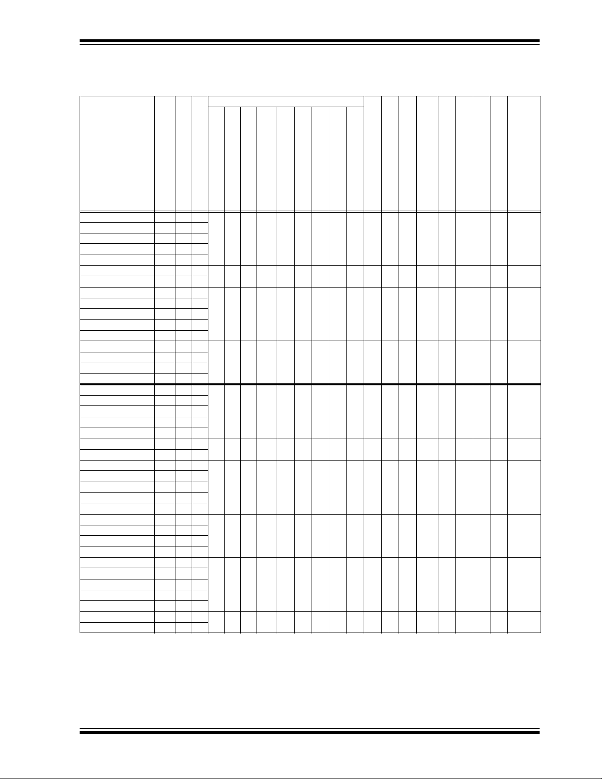
TABLE 1: dsPIC33EPXXXGP50X and PIC24EPXXXGP20X GENERAL PURPOSE FAMILIES
Remappable Peripherals
(3)
Device
RAM (Kbyte)
Page Erase Size (Instructions)
Program Flash Memory (Kbytes)
PIC24EP32GP202 512 32 4
PIC24EP64GP202 1024 64 8
PIC24EP128GP202 1024 128 16
PIC24EP256GP202 1024 256 32
PIC24EP512GP202 1024 512 48
PIC24EP32GP203 512 32 4
PIC24EP64GP203 1024 64 8
PIC24EP32GP204 512 32 4
PIC24EP64GP204 1024 64 8
PIC24EP128GP204 1024 128 16
PIC24EP256GP204 1024 256 32
PIC24EP512GP204 1024 512 48
PIC24EP64GP206 1024 64 8
PIC24EP128GP206 1024 128 16
PIC24EP256GP206 1024 256 32
PIC24EP512GP206 1024 512 48
dsPIC33EP32GP502 512 32 4
dsPIC33EP64GP502 1024 64 8
dsPIC33EP128GP502 1024 128 16
dsPIC33EP256GP502 1024 256 32
dsPIC33EP512GP502 1024 512 48
dsPIC33EP32GP503 512 32 4
dsPIC33EP64GP503 1024 64 8
dsPIC33EP32GP504 512 32 4
dsPIC33EP64GP504 1024 64 8
dsPIC33EP128GP504 1024 128 16
dsPIC33EP256GP504 1024 256 32
dsPIC33EP512GP504 1024 512 48
dsPIC33EP64GP506 1024 64 8
dsPIC33EP128GP506 1024 128 16
dsPIC33EP256GP506 1024 256 32
dsPIC33EP512GP506 1024 512 48
Note 1: On 28-pin devices, Comparator 4 does not have external connections. Refer to Section 25.0 “Op amp/Comparator Module” for details.
2: Only SPI2 is remappable.
3: INT0 is not remappable.
4: The SSOP and VTLA packages are not available for devices with 512 KB of memory.
Input Capture
16-bit/32-bit Timers
54422—32162/3
54422—32183/4YesYes2536VTLA
54422—32193/4YesYes3544
54422—321163/4YesYes5364
54422132162/3
54422132183/4YesYes2536VTLA
54422132193/4YesYes3544
544221321163/4YesYes5364
Output Compare
UART
(2)
SPI
ECAN™ Technology
C™
2
I
CRC Generator
External Interrupts
Op amps/Comparators
10-bit/12-bit ADC (Channels)
(1)
(1)
PTG
CTMU
Yes Yes 21 28
Yes Yes 21 28
I/O Pins
Pins
SPDIP,
SOIC,
SSOP
QFN-S
VTLA
TQFP,
QFN
TQFP,
QFN
SPDIP,
SOIC,
SSOP
QFN-S
VTLA
TQFP,
QFN
TQFP,
QFN
Packages
(4)
(4)
(4)
(4)
,
,
,
,
DS70657E-page 2 Preliminary © 2011-2012 Microchip Technology Inc.
dsPIC33EPXXXGP50X, dsPIC33EPXXXMC20X/50X, AND PIC24EPXXXGP/MC20X
TABLE 2: dsPIC33EPXXXMC20X/50X and PIC24EPXXXMC20X MOTOR CONTROL
FAMILIES
Remappable Peripherals
Device
Page Erase Size (Instructions)
Program Flash Memory (Kbytes)
RAM (Kbytes)
16-bit/32-bit Timers
Input Capture
Output Compare
(4)
Motor Control PWM
(2)
SPI
UART
(Channels)
Quadrature Encoder Interface
ECAN™ Technology
(3)
C™
2
I
CTMU
PTG
I/O Pins
Pins
Packages
CRC Generator
External Interrupts
Op am ps/Co mparators
10-bit/12-bit ADC (Channels)
PIC24EP32MC202 512 32 4
PIC24EP64MC202 1024 64 8
PIC24EP128MC202 1024 128 16
PIC24EP256MC202 1024 256 32
544 6 122—32162/3
(1)
Yes Yes 21 28
SPDIP,
SOIC,
SSOP
QFN-S
(5)
PIC24EP512MC202 1024 512 48
PIC24EP32MC203 512 32 4
PIC24EP64MC203 1024 64 8
5 4 4 6 1 2 2 — 3 2 1 8 3/4 Yes Yes 25 36 VTLA
PIC24EP32MC204 512 32 4
PIC24EP64MC204 1024 64 8
PIC24EP128MC204 1024 128 16
PIC24EP256MC204 1024 256 32
5 4 4 6 1 2 2 — 3 2 1 9 3/4 Yes Yes 35 44
VTLA
TQFP,
QFN
(5)
PIC24EP512MC204 1024 512 48
PIC24EP64MC206 1024 64 8
PIC24EP128MC206 1024 128 16
PIC24EP256MC206 1024 256 32
5 4 4 6 1 2 2 — 3 2 1 16 3/4 Yes Yes 53 64
TQFP,
QFN
PIC24EP512MC206 1024 512 48
dsPIC33EP32MC202 512 32 4
dsPIC33EP64MC202 1024 64 8
dsPIC33EP128MC202 1024 128 16
dsPIC33EP256MC202 1024 256 32
544 6 122—32162/3
(1)
Yes Yes 21 28
SPDIP,
SOIC,
SSOP
QFN-S
(5)
dsPIC33EP512MC202 1024 512 48
dsPIC33EP32MC203 512 32 4
dsPIC33EP64MC203 1024 64 8
5 4 4 6 1 2 2 — 3 2 1 8 3/4 Yes Yes 25 36 VTLA
dsPIC33EP32MC204 512 32 4
dsPIC33EP64MC204 1024 64 8
dsPIC33EP128MC204 1024 128 16
dsPIC33EP256MC204 1024 256 32
5 4 4 6 1 2 2 — 3 2 1 9 3/4 Yes Yes 35 44
VTLA
TQFP,
QFN
(5)
dsPIC33EP512MC204 1024 512 48
dsPIC33EP64MC206 1024 64 8
dsPIC33EP128MC206 1024 128 16
dsPIC33EP256MC206 1024 256 32
5 4 4 6 1 2 2 — 3 2 1 16 3/4 Yes Yes 53 64
TQFP,
QFN
dsPIC33EP512MC206 1024 512 48
dsPIC33EP32MC502 512 32 4
dsPIC33EP64MC502 1024 64 8
dsPIC33EP128MC502 1024 128 16
dsPIC33EP256MC502 1024 256 32
544 6 122132162/3
(1)
Yes Yes 21 28
SPDIP,
SOIC,
SSOP
QFN-S
(5)
dsPIC33EP512MC502 1024 512 48
dsPIC33EP32MC503 512 32 4
dsPIC33EP64MC503 1024 64 8
5 4 4 6 1 2 2 1 3 2 1 8 3/4 Yes Yes 25 36 VTLA
Note 1: On 28-pin devices, Comparator 4 does not have external connections. Refer to Section 25.0 “Op amp/Comparator Module” for details.
2: Only SPI2 is remappable.
3: INT0 is not remappable.
4: Only the PWM Faults are remappable.
5: The SSOP and VTLA packages are not available for devices with 512 KB of memory.
,
,
,
,
,
© 2011-2012 Microchip Technology Inc. Preliminary DS70657E-page 3
dsPIC33EPXXXGP50X, dsPIC33EPXXXMC20X/50X, AND PIC24EPXXXGP/MC20X
TABLE 2: dsPIC33EPXXXMC20X/50X and PIC24EPXXXMC20X MOTOR CONTROL
FAMILIES (CONTINUED)
Remappable Peripherals
(4)
Device
RAM (Kbytes)
Page Erase Size (Instructions)
Program Flash Memory (Kbytes)
dsPIC33EP32MC504 512 32 4
dsPIC33EP64MC504 1024 64 8
dsPIC33EP128MC504 1024 128 16
dsPIC33EP256MC504 1024 256 32
dsPIC33EP512MC504 1024 512 48
dsPIC33EP64MC506 1024 64 8
dsPIC33EP128MC506 1024 128 16
dsPIC33EP256MC506 1024 256 32
dsPIC33EP512MC506 1024 512 48
Note 1: On 28-pin devices, Comparator 4 does not have external connections. Refer to Section 25.0 “Op amp/Comparator Module” for details.
2: Only SPI2 is remappable.
3: INT0 is not remappable.
4: Only the PWM Faults are remappable.
5: The SSOP and VTLA packages are not available for devices with 512 KB of memory.
Input Capture
16-bit/32-bit Timers
5 4 4 6 1 2 2 1 3 2 1 9 3/4 Yes Yes 35 44
5 4 4 6 1 2 2 1 3 2 1 16 3/4 Yes Yes 53 64
(Channels)
Output Compare
Motor Control PWM
Quadrature Encoder Interface
UART
(2)
SPI
ECAN™ Technology
(3)
C™
2
I
CRC Generator
External Interrupts
Op amps/Comparators
10-bit/12-bit ADC (Channels)
CTMU
PTG
I/O Pins
Pins
VTLA
TQFP,
QFN
TQFP,
QFN
Packages
(5)
,
DS70657E-page 4 Preliminary © 2011-2012 Microchip Technology Inc.
dsPIC33EPXXXGP50X, dsPIC33EPXXXMC20X/50X, AND PIC24EPXXXGP/MC20X
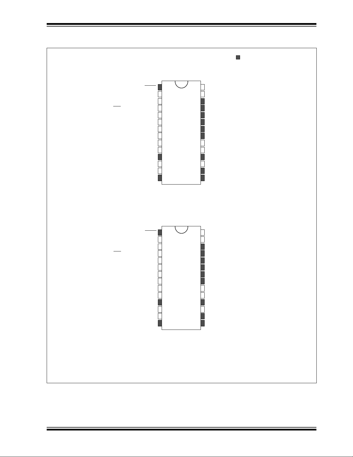
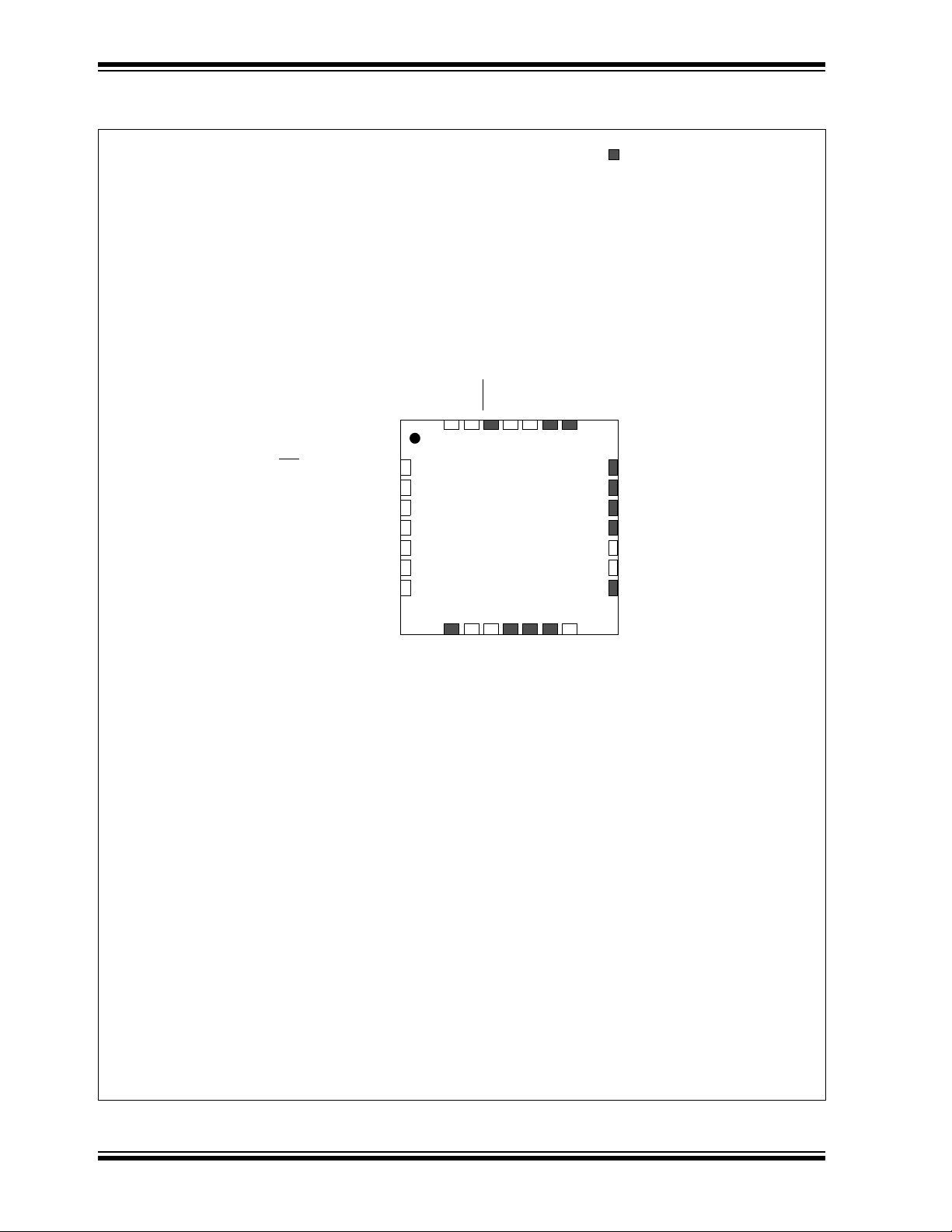
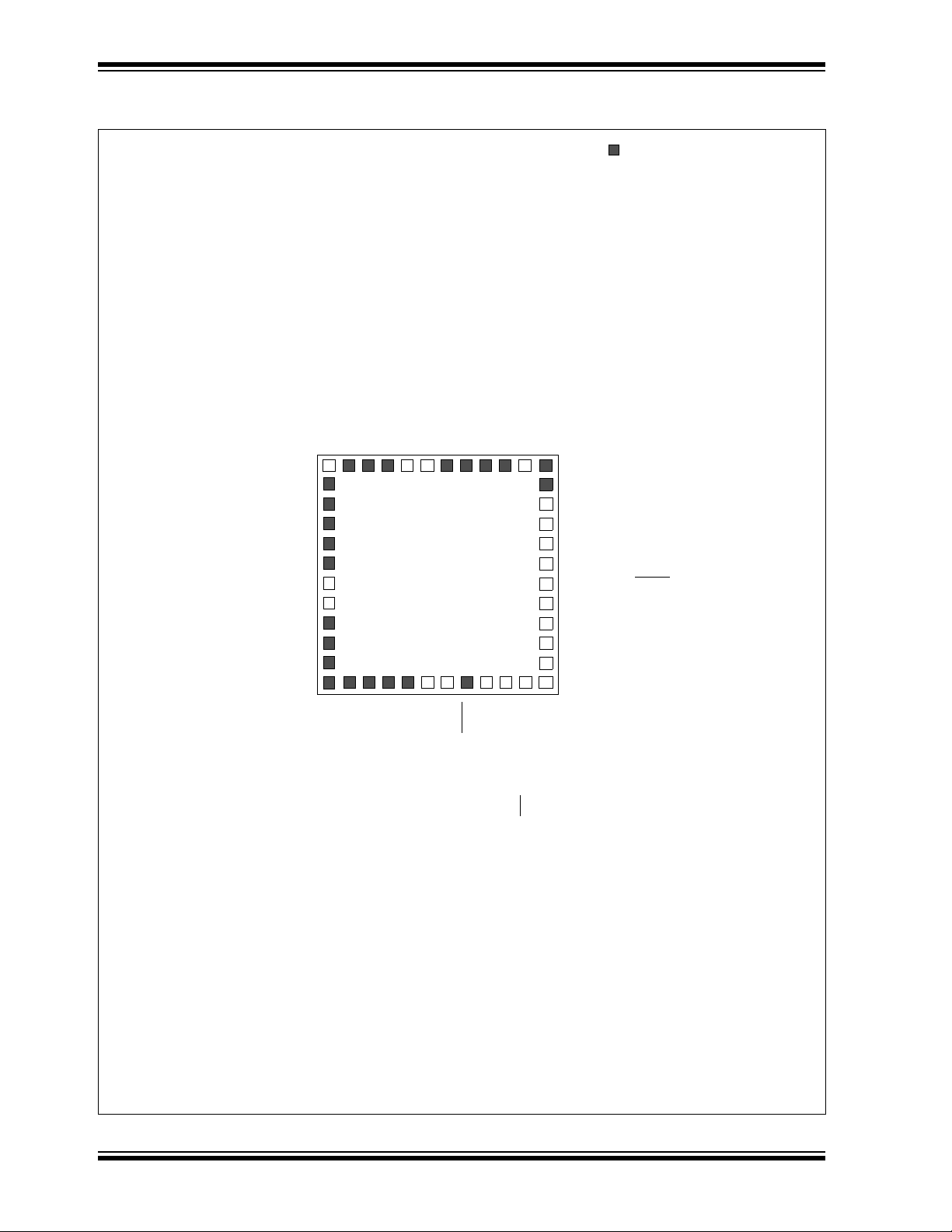
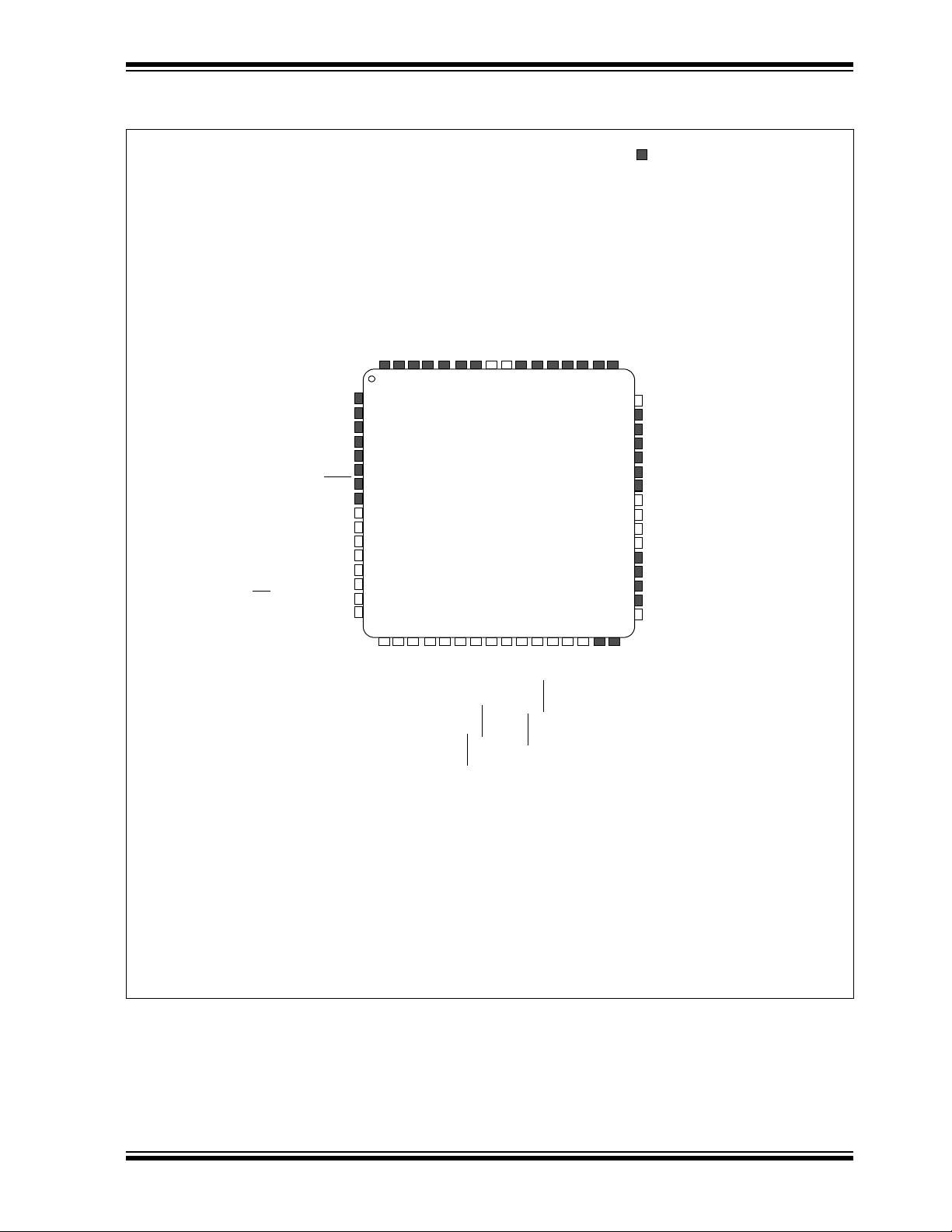
28-Pin SPDIP/SOIC/SSOP
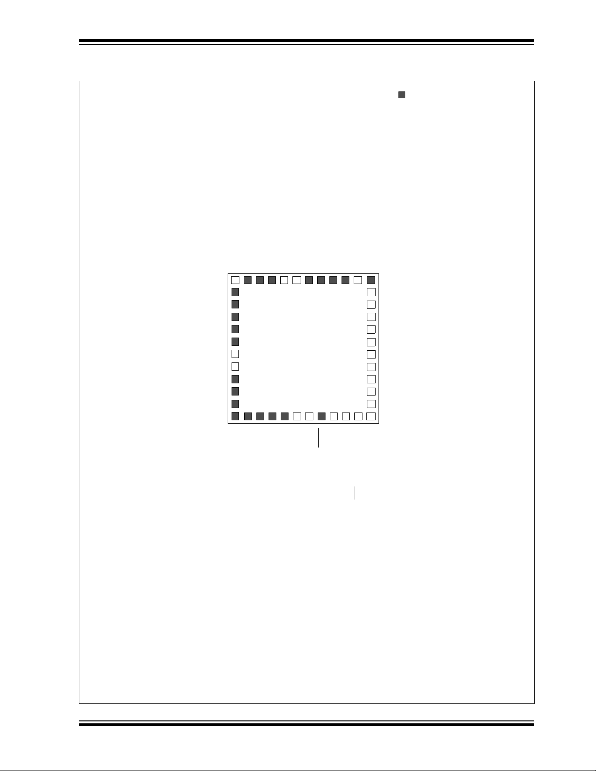
Note 1: The RPn/RPIn pins can be used by any remappable peripheral with some limitation. See Section 11.4
“Peripheral Pin Select” for available peripherals and for information on limitations.
2: Every I/O port pin (RAx-RGx) can be used as change notification (CNAx-CNGx). See Section 11.0
“I/O Ports” for more information.
= Pins are up to 5V tolerant
128
227
326
425
524
623
722
821
920
10 19
11 18
12 17
13 16
14 15
PIC24EPXXXGP202
dsPIC33EPXXXGP502
MCLR AVDD
AN0/OA2OUT/RA0 AVSS
AN1/C2IN1+/RA1 RPI47/T5CK/RB15
PGED3/V
REF-/AN2/C2IN1-/SS1/RPI32/CTED2/RB0 RPI46/T3CK/RB14
PGEC3/V
REF+/AN3/OA1OUT/RPI33/CTED1/RB1 RPI45/CTPLS/RB13
PGEC1/AN4/C1IN1+/RPI34/RB2 RPI44/RB12
PGED1/AN5/C1IN1-/RP35/RB3 TDI/RP43/RB11
TDO/RP42/RB10
OSC1/CLKI/RA2 V
CAP
OSC2/CLKO/RA3 VSS
RP36/RB4 TMS/ASDA1/SDI1/RP41/RB9
CV
REF2O/RP20/T1CK/RA4 TCK/CVREF1O/ASCL1/SDO1/RP40/T4CK/RB8
V
DD SCK1/RP39/INT0/RB7
PGED2/ASDA2/RP37/RB5 PGEC2/ASCL2/RP38/RB6
V
SS
128
227
326
425
524
623
722
821
920
10 19
11 18
12 17
13 16
14 15
PIC24EPXXXMC202
dsPIC33EPXXXMC202/502
MCLR AVDD
AN0/OA2OUT/RA0 AVSS
AN1/C2IN1+/RA1 RPI47/PWM1L/T5CK/RB15
PGED3/V
REF-/AN2/C2IN1-/SS1/RPI32/CTED2/RB0 RPI46/PWM1H/T3CK/RB14
PGEC3/V
REF+/AN3/OA1OUT/RPI33/CTED1/RB1 RPI45/PWM2L/CTPLS/RB13
PGEC1/AN4/C1IN1+/RPI34/RB2 RPI44/PWM2H/RB12
PGED1/AN5/C1IN1-/RP35/RB3 TDI/RP43/PWM3L/RB11
TDO/RP42/PWM3H/RB10
OSC1/CLKI/RA2 V
CAP
OSC2/CLKO/RA3 VSS
FLT32/RP36/RB4 TMS/ASDA1/SDI1/RP41/RB9
CV
REF2O/RP20/T1CK/RA4 TCK/CVREF1O/ASCL1/SDO1/RP40/T4CK/RB8
V
DD SCK1/RP39/INT0/RB7
PGED2/ASDA2/RP37/RB5 PGEC2/ASCL2/RP38/RB6
V
SS
Pin Diagrams
© 2011-2012 Microchip Technology Inc. Preliminary DS70657E-page 5
dsPIC33EPXXXGP50X, dsPIC33EPXXXMC20X/50X, AND PIC24EPXXXGP/MC20X
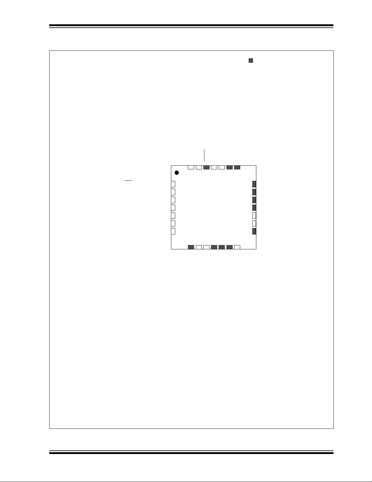
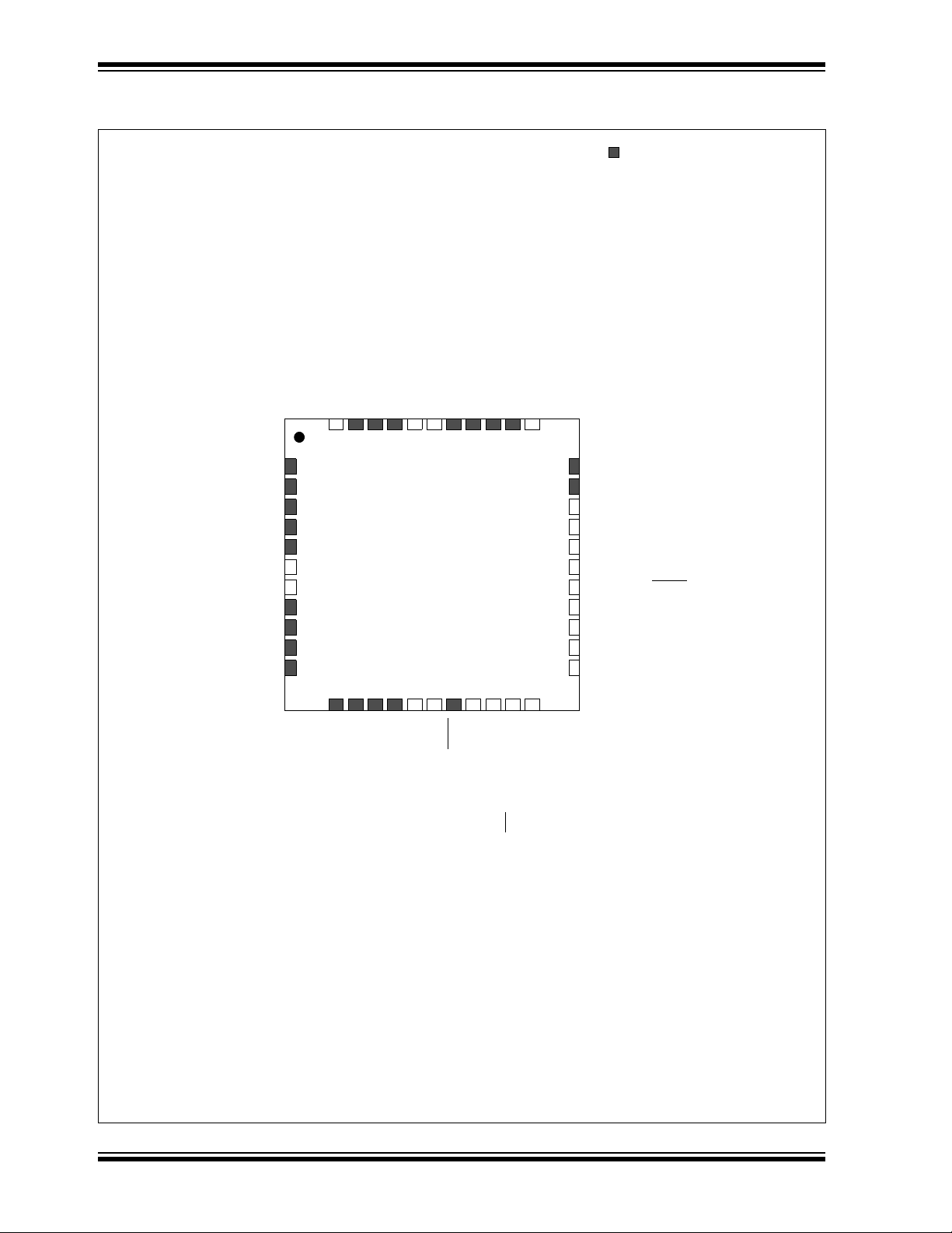
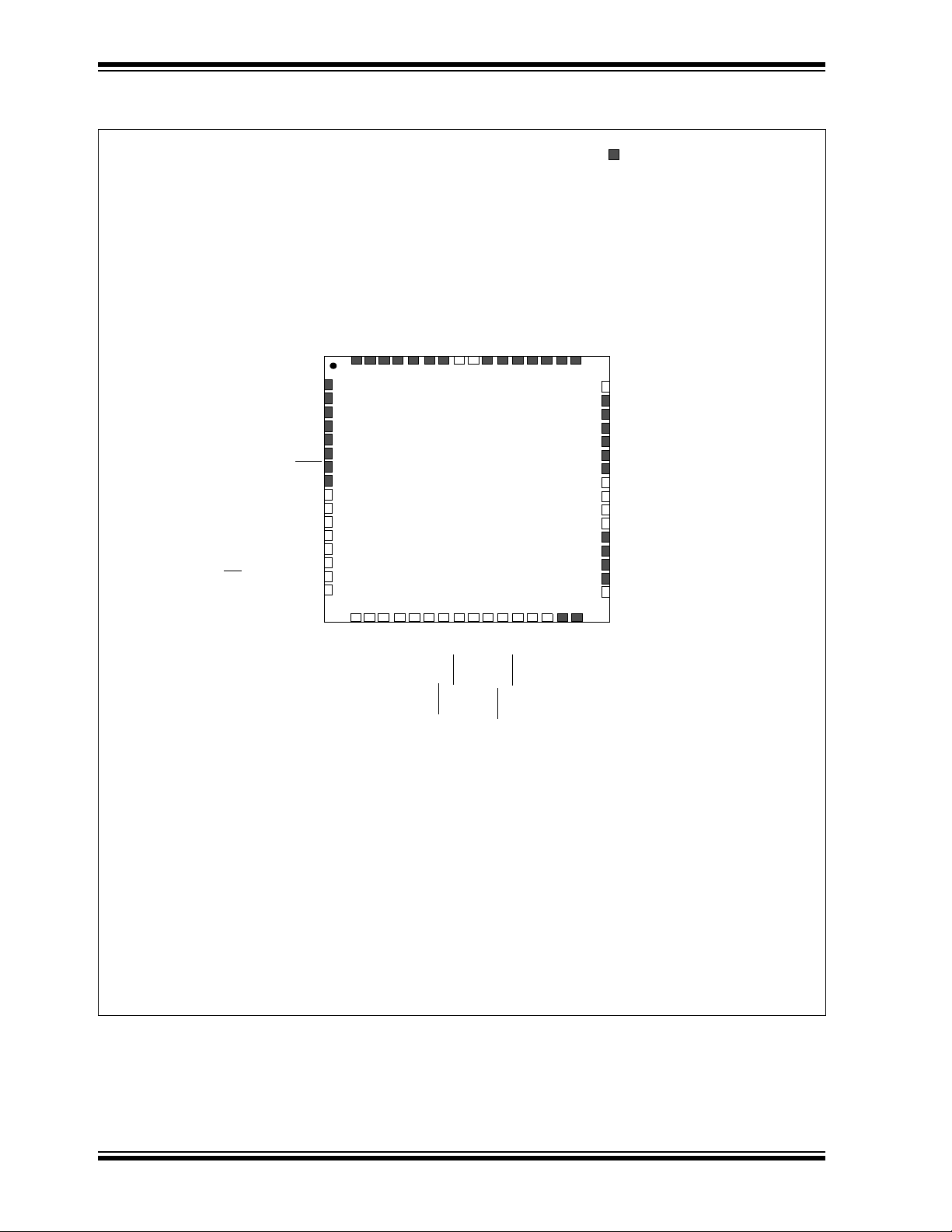
28-Pin QFN-S
(3)
= Pins are up to 5V tolerant
28 27 26 25 24 23 22
8 9 10 11 12 13 14
3
18
17
16
15
4
5
7
1
2 20
19
6
21
PIC24EPXXXGP202
dsPIC33EPXXXGP502
TCK/CVREF1O/ASCL1/SDO1/RP40/T4CK/RB8
SCK1/RP39/INT0/RB7
PGEC2/ASCL2/RP38/RB6
PGED2/ASDA2/RP37/RB5
V
DD
CVREF2O/RP20/T1CK/RA4
RP36/RB4
RPI45/CTPLS/RB13
RPI44/RB12
TDI/RP43/RB11
TDO/RP42/RB10
V
CAP
VSS
TMS/ASDA1/SDI1/RP41/RB9
RPI46/T3CK/RB14
RPI47/T5CK/RB15
AV
SS
AVDD
MCLR
AN0/OA2OUT/RA0
AN1/C2IN1+/RA1
PGED3/VREF-/AN2/C2IN1-/SS1/RPI32/CTED2/RB0
PGEC3/V
REF+/AN3/OA1OUT/RPI33/CTED1/RB1
V
SS
OSC1/CLKI/RA2
OSC2/CLKO/RA3
PGEC1/AN4/C1IN1+/RPI34/RB2
PGED1/AN5/C1IN1-/RP35/RB3
Note 1: The RPn/RPIn pins can be used by any remappable peripheral with some limitation. See Section 11.4
“Peripheral Pin Select” for available peripherals and for information on limitations.
2: Every I/O port pin (RAx-RGx) can be used as change notification (CNAx-CNGx). See Section 11.0
“I/O Ports” for more information.
3: The metal pad at the bottom of the device is not connected to any pins and is recommended to be
connected to V
SS externally.
Pin Diagrams (Continued)
DS70657E-page 6 Preliminary © 2011-2012 Microchip Technology Inc.
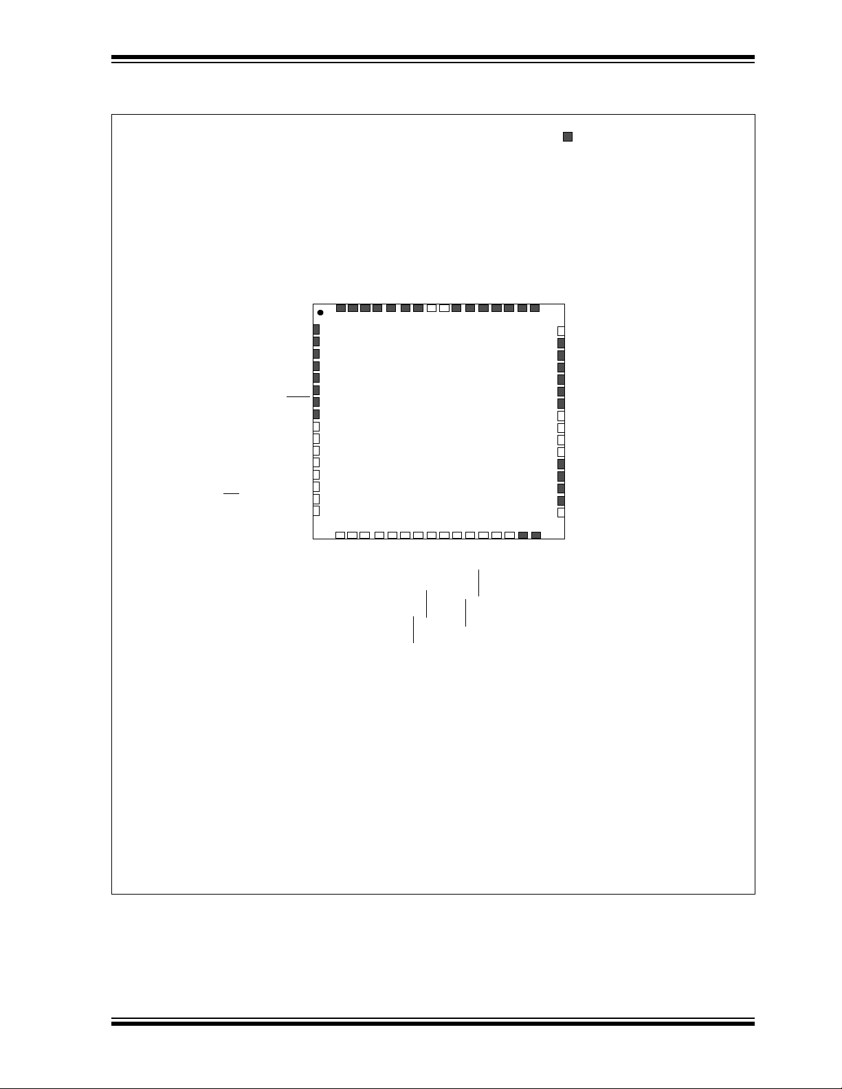
dsPIC33EPXXXGP50X, dsPIC33EPXXXMC20X/50X, AND PIC24EPXXXGP/MC20X
28-Pin QFN-S
(3)
= Pins are up to 5V tolerant
28 27 26 25 24 23 22
8 9 10 11 12 13 14
3
18
17
16
15
4
5
7
1
2 20
19
6
21
PIC24EPXXXMC202
dsPIC33EPXXXMC202/502
TCK/CVREF1O/ASCL1/SDO1/RP40/T4CK/RB8
SCK1/RP39/INT0/RB7
PGEC2/ASCL2/RP38/RB6
PGED2/ASDA2/RP37/RB5
V
DD
CVREF2O/RP20/T1CK/RA4
FLT32/RP36/RB4
RPI45/PWM2L/CTPLS/RB13
RPI44/PWM2H/RB12
TDI/RP43/PWM3L/RB11
TDO/RP42/PWM3H/RB10
V
CAP
VSS
TMS/ASDA1/SDI1/RP41/RB9
RPI46/PWM1H/T3CK/RB14
RPI47/PWM1L/T5CK/RB15
AV
SS
AVDD
MCLR
AN0/OA2OUT/RA0
AN1/C2IN1+/RA1
PGED3/VREF-/AN2/C2IN1-/SS1/RPI32/CTED2/RB0
PGEC3/V
REF+/AN3/OA1OUT/RPI33/CTED1/RB1
V
SS
OSC1/CLKI/RA2
OSC2/CLKO/RA3
PGEC1/AN4/C1IN1+/RPI34/RB2
PGED1/AN5/C1IN1-/RP35/RB3
Note 1: The RPn/RPIn pins can be used by any remappable peripheral with some limitation. See Section 11.4
“Peripheral Pin Select” for available peripherals and for information on limitations.
2: Every I/O port pin (RAx-RGx) can be used as change notification (CNAx-CNGx). See Section 11.0
“I/O Ports” for more information.
3: The metal pad at the bottom of the device is not connected to any pins and is recommended to be
connected to V
SS externally.
Pin Diagrams (Continued)
© 2011-2012 Microchip Technology Inc. Preliminary DS70657E-page 7

dsPIC33EPXXXGP50X, dsPIC33EPXXXMC20X/50X, AND PIC24EPXXXGP/MC20X
36-Pin VTLA
(3)
1
10
33 32 31 30 29 28
2
3
4
5
6
24
23
22
21
20
19
11 12 13 14 15
7
8
9
34
35
36
16
17
18
27
26
25
= Pins are up to 5V tolerant
PIC24EP32GP203
TCK/CVREF1O/ASCL1/SDO1/RP40/T4CK/RB8
RPI45/CTPLS/RB13
PGEC1/AN4/C1IN1+/RPI34/RB2
PGED1/AN5/C1IN1-/RP35/RB3
AN6/OA3OUT/C4IN1+/OCFB/RC0
AN7/C3IN1-/C4IN1-/RC1
V
DD
VSS
OSC1/CLKI/RA2
OSC2/CLKO/RA3
SDA2/RPI24/RA8
RPI46/T3CK/RB14
RPI47/T5CK/RB15
AV
SS
AVDD
MCLR
AN0/OA2OUT/RA0
AN1/C2IN1+/RA1
PGED3/V
REF-/AN2/C2IN1-/SS1/RPI32/CTED2/RB0
PGEC3/V
REF+/AN3/OA1OUT/RPI33/CTED1/RB1
RPI44/RB12
TDI/RP43/RB11
TDO/RP42/RB10
V
CAP
VSS
RP56/RC8
TMS/ASDA1/SDI1/RP41/RB9
SCK1/RP39/INT0/RB7
PGEC2/ASCL2/RP38/RB6
PGED2/ASDA2/RP37/RB5
V
DD
VSS
CVREF2O/RP20/T1CK/RA4
V
DD
SCL2/RP36/RB4
VDD
Note 1: The RPn/RPIn pins can be used by any remappable peripheral with some limitation. See Section 11.4
“Peripheral Pin Select” for available peripherals and for information on limitations.
2: Every I/O port pin (RAx-RGx) can be used as change notification (CNAx-CNGx). See Section 11.0
“I/O Ports” for more information.
3: The metal pad at the bottom of the device is not connected to any pins and is recommended to be
connected to V
SS externally.
dsPIC33EP32GP503
PIC24EP64GP203
dsPIC33EP64GP503
Pin Diagrams (Continued)
DS70657E-page 8 Preliminary © 2011-2012 Microchip Technology Inc.

dsPIC33EPXXXGP50X, dsPIC33EPXXXMC20X/50X, AND PIC24EPXXXGP/MC20X
36-Pin VTLA
(3)
= Pins are up to 5V tolerant
1
10
33 32 31 30 29 28
2
3
4
5
6
24
23
22
21
20
19
11 12 13 14 15
7
8
9
34
35
36
16
17
18
27
26
25
PIC24EP32MC203
TCK/CVREF1O/ASCL1/SDO1/RP40/T4CK/RB8
RPI45/PWM2L/CTPLS/RB13
PGEC1/AN4/C1IN1+/RPI34/RB2
PGED1/AN5/C1IN1-/RP35/RB3
AN6/OA3OUT/C4IN1+/OCFB/RC0
AN7/C3IN1-/C4IN1-/RC1
V
DD
VSS
OSC1/CLKI/RA2
OSC2/CLKO/RA3
SDA2/RPI24/RA8
RPI46/PWM1H/T3CK/RB14
RPI47/PWM1L/T5CK/RB15
AV
SS
AVDD
MCLR
AN0/OA2OUT/RA0
AN1/C2IN1+/RA1
PGED3/V
REF-/AN2/C2IN1-/SS1/RPI32/CTED2/RB0
PGEC3/V
REF+/AN3/OA1OUT/RPI33/CTED1/RB1
RPI44/PWM2H/RB12
TDI/RP43/PWM3L/RB11
TDO/RP42/PWM3H/RB10
V
CAP
VSS
RP56/RC8
TMS/ASDA1/SDI1/RP41/RB9
SCK1/RP39/INT0/RB7
PGEC2/ASCL2/RP38/RB6
PGED2/ASDA2/RP37/RB5
V
DD
VSS
CVREF2O/RP20/T1CK/RA4
V
DD
FLT32/SCL2/RP36/RB4
VDD
Note 1: The RPn/RPIn pins can be used by any remappable peripheral with some limitation. See Section 11.4
“Peripheral Pin Select” for available peripherals and for information on limitations.
2: Every I/O port pin (RAx-RGx) can be used as change notification (CNAx-CNGx). See Section 11.0
“I/O Ports” for more information.
3: The metal pad at the bottom of the device is not connected to any pins and is recommended to be
connected to V
SS externally.
dsPIC33EP32MC203/503
PIC24EP64MC203
dsPIC33EP64MC203/503
Pin Diagrams (Continued)
© 2011-2012 Microchip Technology Inc. Preliminary DS70657E-page 9
dsPIC33EPXXXGP50X, dsPIC33EPXXXMC20X/50X, AND PIC24EPXXXGP/MC20X
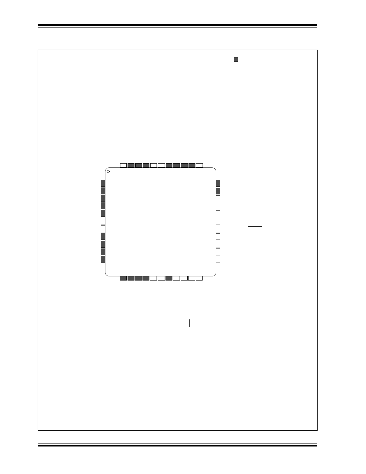
44-Pin TQFP
= Pins are up to 5V tolerant
4443424140393837363534
133
232
331
430
529
628
727
826
925
10 24
11 23
1213141516171819202122
PIC24EPXXXGP204
TCK/CVREF1O/ASCL1/RP40/T4CK/RB8TDO/RA10
RPI45/CTPLS/RB13
PGEC1/AN4/C1IN1+/RPI34/RB2
PGED1/AN5/C1IN1-/RP35/RB3
AN6/OA3OUT/C4IN1+/OCFB/RC0
AN7/C3IN1-/C4IN1-/RC1
AN8/C3IN1+/U1RTS
/BCLK1/RC2
V
DD
VSS
OSC1/CLKI/RA2
OSC2/CLKO/RA3
SDA2/RPI24/RA8
SCL2/RP36/RB4
TDI/RA7
RPI46/T3CK/RB14
RPI47/T5CK/RB15
AV
SS
AVDD
MCLR
AN0/OA2OUT/RA0
AN1/C2IN1+/RA1
PGED3/V
REF-/AN2/C2IN1-/SS1/RPI32/CTED2/RB0
PGEC3/V
REF+/AN3/OA1OUT/RPI33/CTED1/RB1
RPI44/RB12
RP43/RB11
RP42/RB10
V
CAP
VSS
RP57/RC9
RP56/RC8
RP55/RC7
RP54/RC6
TMS/ASDA1/RP41/RB9
RP39/INT0/RB7
PGEC2/ASCL2/RP38/RB6
PGED2/ASDA2/RP37/RB5
VDDVSS
SCL1/RPI53/RC5
SDA1/RPI52/RC4
SCK1/RPI51/RC3
SDI1/RPI25/RA9
CV
REF2O/SDO1/RP20/T1CK/RA4
Note 1: The RPn/RPIn pins can be used by any remappable peripheral with some limitation. See Section 11.4
“Peripheral Pin Select” for available peripherals and for information on limitations.
2: Every I/O port pin (RAx-RGx) can be used as change notification (CNAx-CNGx). See Section 11.0
“I/O Ports” for more information.
dsPIC33EPXXXGP504
Pin Diagrams (Continued)
DS70657E-page 10 Preliminary © 2011-2012 Microchip Technology Inc.
dsPIC33EPXXXGP50X, dsPIC33EPXXXMC20X/50X, AND PIC24EPXXXGP/MC20X
44-Pin TQFP
= Pins are up to 5V tolerant
4443424140393837363534
133
232
331
430
529
628
727
826
925
10 24
11 23
1213141516171819202122
PIC24EPXXXMC204
TCK/CVREF1O/ASCL1/RP40/T4CK/RB8TDO/RA10
RPI45/PWM2L/CTPLS/RB13
PGEC1/AN4/C1IN1+/RPI34/RB2
PGED1/AN5/C1IN1-/RP35/RB3
AN6/OA3OUT/C4IN1+/OCFB/RC0
AN7/C3IN1-/C4IN1-/RC1
AN8/C3IN1+/U1RTS
/BCLK1/FLT3/RC2
V
DD
VSS
OSC1/CLKI/RA2
OSC2/CLKO/RA3
SDA2/RPI24/RA8
FLT32/SCL2/RP36/RB4
TDI/RA7
RPI46/PWM1H/T3CK/RB14
RPI47/PWM1L/T5CK/RB15
AV
SS
AVDD
MCLR
AN0/OA2OUT/RA0
AN1/C2IN1+/RA1
PGED3/V
REF-/AN2/C2IN1-/SS1/RPI32/CTED2/RB0
PGEC3/V
REF+/AN3/OA1OUT/RPI33/CTED1/RB1
RPI44/PWM2H/RB12
RP43/PWM3L/RB11
RP42/PWM3H/RB10
V
CAP
VSS
RP57/RC9
RP56/RC8
RP55/RC7
RP54/RC6
TMS/ASDA1/RP41/RB9
RP39/INT0/RB7
PGEC2/ASCL2/RP38/RB6
PGED2/ASDA2/RP37/RB5
VDDVSS
SCL1/RPI53/RC5
SDA1/RPI52/RC4
SCK1/RPI51/RC3
SDI1/RPI25/RA9
CV
REF2O/SDO1/RP20/T1CK/RA4
Note 1: The RPn/RPIn pins can be used by any remappable peripheral with some limitation. See Section 11.4
“Peripheral Pin Select” for available peripherals and for information on limitations.
2: Every I/O port pin (RAx-RGx) can be used as change notification (CNAx-CNGx). See Section 11.0
“I/O Ports” for more information.
dsPIC33EPXXXMC204/504
Pin Diagrams (Continued)
© 2011-2012 Microchip Technology Inc. Preliminary DS70657E-page 11
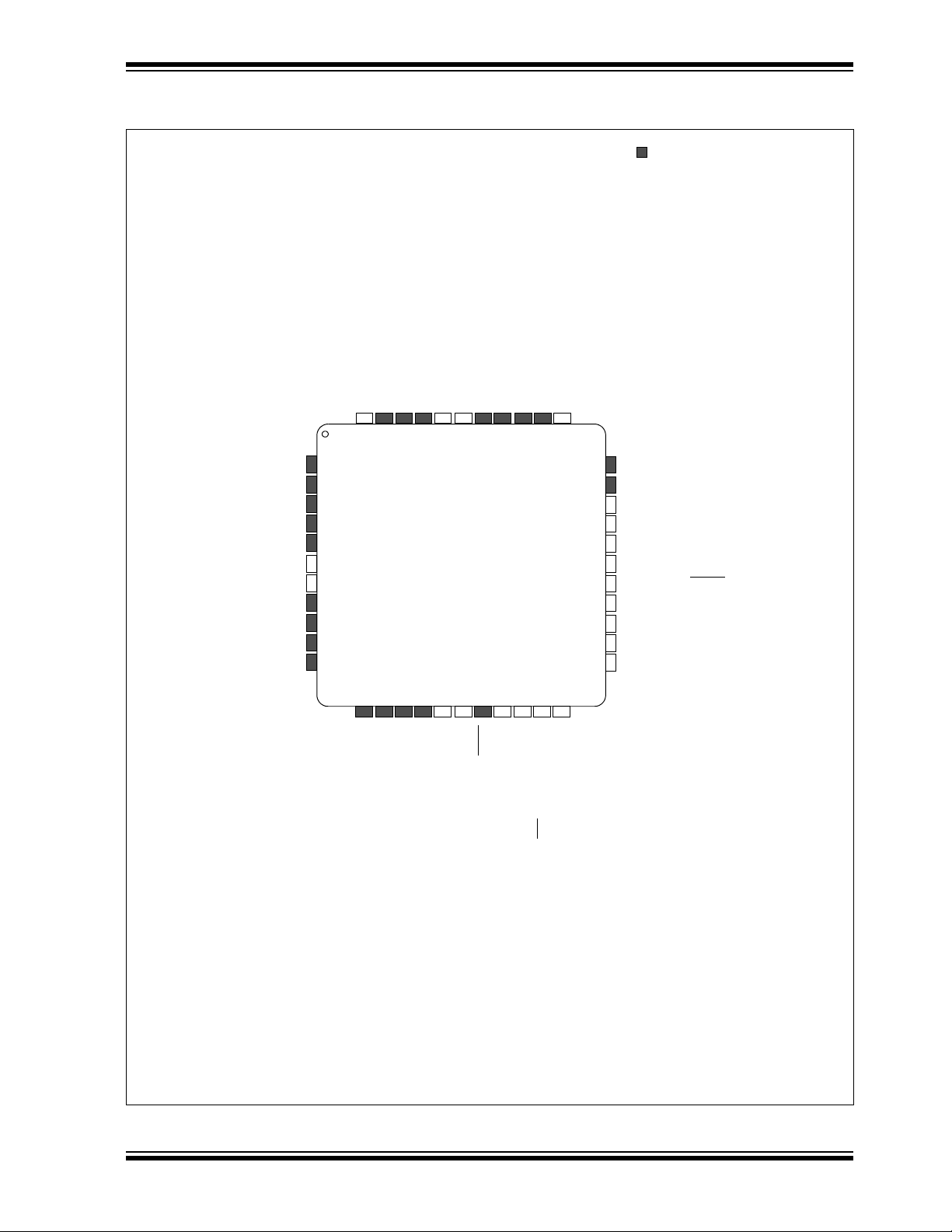
dsPIC33EPXXXGP50X, dsPIC33EPXXXMC20X/50X, AND PIC24EPXXXGP/MC20X
44-Pin VTLA
(3)
= Pins are up to 5V tolerant
PIC24EPXXXGP204
1
12
41 40 39 38 37 36 35 34
2
3
4
5
6
7
8
30
29
28
27
26
25
24
23
13 14 15 16 17 18 19
9
10
11
2220
21
33
32
31
424344
PGEC1/AN4/C1IN1+/RPI34/RB2
PGED1/AN5/C1IN1-/RP35/RB3
AN6/OA3OUT/C4IN1+/OCFB/RC0
AN7/C3IN1-/C4IN1-/RC1
AN8/C3IN1+/U1RTS
/BCLK1/RC2
V
DD
VSS
OSC1/CLKI/RA2
OSC2/CLKO/RA3
SDA2/RPI24/RA8
SCL2/RP36/RB4
TCK/CVREF1O/ASCL1/RP40/T4CK/RB8
RP39/INT0/RB7
PGEC2/ASCL2/RP38/RB6
PGED2/ASDA2/RP37/RB5
V
DD
VSS
SCL1/RPI53/RC5
SDA1/RPI52/RC4
SCK1/RPI51/RC3
SDI1/RPI25/RA9
CVREF2O/SDO1/RP20/T1CK/RA4
RPI45/CTPLS/RB13
RPI44/RB12
RP43/RB11
RP42/RB10
V
CAP
VSS
RP57/RC9
RP56/RC8
RP55/RC7
RP54/RC6
TMS/ASDA1/RP41/RB9
TDO/RA10
TDI/RA7
RPI46/T3CK/RB14
RPI47/T5CK/RB15
AV
SS
AVDD
MCLR
AN0/OA2OUT/RA0
AN1/C2IN1+/RA1
PGED3/V
REF-/AN2/C2IN1-/SS1/RPI32/CTED2/RB0
PGEC3/V
REF+/AN3/OA1OUT/RPI33/CTED1/RB1
Note 1: The RPn/RPIn pins can be used by any remappable peripheral with some limitation. See Section 11.4
“Peripheral Pin Select” for available peripherals and for information on limitations.
2: Every I/O port pin (RAx-RGx) can be used as change notification (CNAx-CNGx). See Section 11.0
“I/O Ports” for more information.
3: The metal pad at the bottom of the device is not connected to any pins and is recommended to be
connected to V
SS externally.
dsPIC33EPXXXGP504
Pin Diagrams (Continued)
DS70657E-page 12 Preliminary © 2011-2012 Microchip Technology Inc.
dsPIC33EPXXXGP50X, dsPIC33EPXXXMC20X/50X, AND PIC24EPXXXGP/MC20X
44-Pin VTLA
(3)
= Pins are up to 5V tolerant
PIC24EPXXXMC204
1
12
41 40 39 38 37 36 35 34
2
3
4
5
6
7
8
30
29
28
27
26
25
24
23
13 14 15 16 17 18 19
9
10
11
22
20
21
33
32
31
424344
PGEC1/AN4/C1IN1+/RPI34/RB2
PGED1/AN5/C1IN1-/RP35/RB3
AN6/OA3OUT/C4IN1+/OCFB/RC0
AN7/C3IN1-/C4IN1-/RC1
AN8/C3IN1+/U1RTS
/BCLK1/FLT3/RC2
V
DD
VSS
OSC1/CLKI/RA2
OSC2/CLKO/RA3
SDA2/RPI24/RA8
FLT32/SCL2/RP36/RB4
TCK/CVREF1O/ASCL1/RP40/T4CK/RB8
RP39/INT0/RB7
PGEC2/ASCL2/RP38/RB6
PGED2/ASDA2/RP37/RB5
V
DD
VSS
SCL1/RPI53/RC5
SDA1/RPI52/RC4
SCK1/RPI51/RC3
SDI1/RPI25/RA9
CV
REF2O/SDO1/RP20/T1CK/RA4
RPI45/PWM2L/CTPLS/RB13
RPI44/PWM2H/RB12
RP43/PWM3L/RB11
RP42/PWM3H/RB10
V
CAP
VSS
RP57/RC9
RP56/RC8
RP55/RC7
RP54/RC6
TMS/ASDA1/RP41/RB9
TDO/RA10
TDI/RA7
RPI46/PWM1H/T3CK/RB14
RPI47/PWM1L/T5CK/RB15
AV
SS
AVDD
MCLR
AN0/OA2OUT/RA0
AN1/C2IN1+/RA1
PGED3/V
REF-/AN2/C2IN1-/SS1/RPI32/CTED2/RB0
PGEC3/V
REF+/AN3/OA1OUT/RPI33/CTED1/RB1
Note 1: The RPn/RPIn pins can be used by any remappable peripheral with some limitation. See Section 11.4
“Peripheral Pin Select” for available peripherals and for information on limitations.
2: Every I/O port pin (RAx-RGx) can be used as change notification (CNAx-CNGx). See Section 11.0
“I/O Ports” for more information.
3: The metal pad at the bottom of the device is not connected to any pins and is recommended to be
connected to V
SS externally.
dsPIC33EPXXXMC204/504
Pin Diagrams (Continued)
© 2011-2012 Microchip Technology Inc. Preliminary DS70657E-page 13
dsPIC33EPXXXGP50X, dsPIC33EPXXXMC20X/50X, AND PIC24EPXXXGP/MC20X
44-Pin QFN
(3)
= Pins are up to 5V tolerant
44 43 42 41 40 39 38 37 36 35
12 13 14 15 16 17 18 19 20 21
3
30
29
28
27
26
25
24
23
4
5
7
8
9
10
11
1
2 32
31
6
22
33
34
PIC24EPXXXGP204
PGEC1/AN4/C1IN1+/RPI34/RB2
PGED1/AN5/C1IN1-/RP35/RB3
AN6/OA3OUT/C4IN1+/OCFB/RC0
AN7/C3IN1-/C4IN1-/RC1
AN8/C3IN1+/U1RTS
/BCLK1/RC2
V
DD
VSS
OSC1/CLKI/RA2
OSC2/CLKO/RA3
SDA2/RPI24/RA8
SCL2/RP36/RB4
TCK/CVREF1O/ASCL1/RP40/T4CK/RB8
RP39/INT0/RB7
PGEC2/ASCL2/RP38/RB6
PGED2/ASDA2/RP37/RB5
VDD
VSS
SCL1/RPI53/RC5
SDA1/RPI52/RC4
SCK1/RPI51/RC3
SDI1/RPI25/RA9
CV
REF2O/SDO1/RP20/T1CK/RA4
RPI45/CTPLS/RB13
RPI44/RB12
RP43/RB11
RP42/RB10
V
CAP
VSS
RP57/RC9
RP56/RC8
RP55/RC7
RP54/RC6
TMS/ASDA1/RP41/RB9
TDO/RA10
TDI/RA7
RPI46/T3CK/RB14
RPI47/T5CK/RB15
AV
SS
AVDD
MCLR
AN0/OA2OUT/RA0
AN1/C2IN1+/RA1
PGED3/V
REF-/AN2/C2IN1-/SS1/RPI32/CTED2/RB0
PGEC3/V
REF+/AN3/OA1OUT/RPI33/CTED1/RB1
Note 1: The RPn/RPIn pins can be used by any remappable peripheral with some limitation. See Section 11.4
“Peripheral Pin Select” for available peripherals and for information on limitations.
2: Every I/O port pin (RAx-RGx) can be used as change notification (CNAx-CNGx). See Section 11.0
“I/O Ports” for more information.
3: The metal pad at the bottom of the device is not connected to any pins and is recommended to be
connected to V
SS externally.
dsPIC33EPXXXGP504
Pin Diagrams (Continued)
DS70657E-page 14 Preliminary © 2011-2012 Microchip Technology Inc.

dsPIC33EPXXXGP50X, dsPIC33EPXXXMC20X/50X, AND PIC24EPXXXGP/MC20X
44-Pin QFN
(3)
= Pins are up to 5V tolerant
44 43 42 41 40 39 38 37 36 35
12 13 14 15 16 17 18 19 20 21
3
30
29
28
27
26
25
24
23
4
5
7
8
9
10
11
1
2 32
31
6
22
33
34
PIC24EPXXXMC204
PGEC1/AN4/C1IN1+/RPI34/RB2
PGED1/AN5/C1IN1-/RP35/RB3
AN6/OA3OUT/C4IN1+/OCFB/RC0
AN7/C3IN1-/C4IN1-/RC1
AN8/C3IN1+/U1RTS
/BCLK1/FLT3/RC2
V
DD
VSS
OSC1/CLKI/RA2
OSC2/CLKO/RA3
SDA2/RPI24/RA8
FLT32/SCL2/RP36/RB4
TCK/CVREF1O/ASCL1/RP40/T4CK/RB8
RP39/INT0/RB7
PGEC2/ASCL2/RP38/RB6
PGED2/ASDA2/RP37/RB5
VDD
VSS
SCL1/RPI53/RC5
SDA1/RPI52/RC4
SCK1/RPI51/RC3
SDI1/RPI25/RA9
CV
REF2O/SDO1/RP20/T1CK/RA4
RPI45/PWM2L/CTPLS/RB13
RPI44/PWM2H/RB12
RP43/PWM3L/RB11
RP42/PWM3H/RB10
V
CAP
VSS
RP57/RC9
RP56/RC8
RP55/RC7
RP54/RC6
TMS/ASDA1/RP41/RB9
TDO/RA10
TDI/RA7
RPI46/PWM1H/T3CK/RB14
RPI47/PWM1L/T5CK/RB15
AV
SS
AVDD
MCLR
AN0/OA2OUT/RA0
AN1/C2IN1+/RA1
PGED3/V
REF-/AN2/C2IN1-/SS1/RPI32/CTED2/RB0
PGEC3/V
REF+/AN3/OA1OUT/RPI33/CTED1/RB1
Note 1: The RPn/RPIn pins can be used by any remappable peripheral with some limitation. See Section 11.4
“Peripheral Pin Select” for available peripherals and for information on limitations.
2: Every I/O port pin (RAx-RGx) can be used as change notification (CNAx-CNGx). See Section 11.0
“I/O Ports” for more information.
3: The metal pad at the bottom of the device is not connected to any pins and is recommended to be
connected to V
SS externally.
dsPIC33EPXXXMC204/504
Pin Diagrams (Continued)
© 2011-2012 Microchip Technology Inc. Preliminary DS70657E-page 15
dsPIC33EPXXXGP50X, dsPIC33EPXXXMC20X/50X, AND PIC24EPXXXGP/MC20X
64-Pin TQFP
= Pins are up to 5V tolerant
646362616059585756555453525150
49
148
247
346
445
544
643
742
841
940
10 39
11 38
12 37
13 36
14 35
15 34
16 33
171819202122232425262728293031
32
TDI/RA7
RPI46/T3CK/RB14
RPI47/T5CK/RB15
RP118/RG6
RPI119/RG7
RP120/RG8
MCLR
RPI121/RG9
V
SS
V
DD
AN10/RPI28/RA12
AN9/RPI27/RA11
AN0/OA2OUT/RA0
AN1/C2IN1+/RA1
PGED3/V
REF
-/AN2/C2IN1-/SS1/RPI32/CTED2/RB0
PGEC3/V
REF
+/AN3/OA1OUT/RPI33/CTED1/RB1
TDO/RA10
RPI45/CTPLS/RB13
RPI44/RB12
RP43/RB11
RP42/RB10
RP97/RF1
RPI96/RF0
VDDV
CAP
RP57/RC9
RD6
RD5
RP56/RC8
RP55/RC7
RP54/RC6
TMS/ASDA1/RP41/RB9
TCK/CV
REF1O
/ASCL1/RP40/T4CK/RB8
RC13
RP39/INT0/RB7
RPI58/RC10
PGEC2/ASCL2/RP38/RB6
PGED2/ASDA2/RP37/RB5
RD8
V
SS
OSC2/CLKO/RC15
OSC1/CLKI/RC12
V
DD
SCL1/RPI53/RC5
SDA1/RPI52/RC4
SCK1/RPI51/RC3
SDI1/RPI25/RA9
CV
REF2O
/SDO1/RP20/T1CK/RA4
PGEC1/AN4/C1IN1+/RPI34/RB2
PGED1/AN5/C1IN1-/RP35/RB3
AV
DD
AV
SS
AN6/OA3OUT/C4IN1+/OCFB/RC0
AN7/C3IN1-/C4IN1-/RC1
AN8/C3IN1+/U1RTS
/BCLK1/RC2
AN11/C1IN2-
(3)
/U1CTS/RC11
V
SS
V
DD
AN12/C2IN2-
(3)
/U2RTS/BCLK2/RE12
AN13/C3IN2-
(3)
/U2CTS/RE13
AN14/RPI94/RE14
AN15/RPI95/RE15
SDA2/RPI24/RA8
SCL2/RP36/RB4
Note 1: The RPn/RPIn pins can be used by any remappable peripheral with some limitation. See Section 11.4
“Peripheral Pin Select” for available peripherals and for information on limitations.
2: Every I/O port pin (RAx-RGx) can be used as change notification (CNAx-CNGx). See Section 11.0 “I/
O Ports” for more information.
3: This pin is not available as an input when OPMODE (CMxCON<10>) = 1.
dsPIC33EP64GP506
PIC24EP64GP206
PIC24EP128GP206
PIC24EP256GP206
dsPIC33EP128GP506
dsPIC33EP256GP506
dsPIC33EP512GP506
PIC24EP512GP206
Pin Diagrams (Continued)
DS70657E-page 16 Preliminary © 2011-2012 Microchip Technology Inc.
dsPIC33EPXXXGP50X, dsPIC33EPXXXMC20X/50X, AND PIC24EPXXXGP/MC20X
64-Pin TQFP
= Pins are up to 5V tolerant
646362616059585756555453525150
49
148
247
346
445
544
643
742
841
940
10 39
11 38
12 37
13 36
14 35
15 34
16 33
171819202122232425262728293031
32
TDI/RA7
RPI46/PWM1H/T3CK/RB14
RPI47/PWM1L/T5CK/RB15
RP118/RG6
RPI119/RG7
RP120/RG8
MCLR
RPI121/RG9
V
SS
V
DD
AN10/RPI28/RA12
AN9/RPI27/RA11
AN0/OA2OUT/RA0
AN1/C2IN1+/RA1
PGED3/
V
REF
-/AN2/C2IN1-/SS1/RPI32/CTED2/RB0
PGEC3/
V
REF
+/AN3/OA1OUT/RPI33/CTED1/RB1
TDO/RA10
RPI45/PWM2L/CTPLS/RB13
RPI44/PWM2H/RB12
RP43/PWM3L/RB11
RP42/PWM3H/RB10
RP97/RF1
RPI96/RF0
VDDV
CAP
RP57/RC9
RD6
RD5
RP56/RC8
RP55/RC7
RP54/RC6
TMS/ASDA1/RP41/RB9
TCK/
CV
REF1O
/ASCL1/RP40/T4CK/RB8
RC13
RP39/INT0/RB7
RPI58/RC10
PGEC2/ASCL2/RP38/RB6
PGED2/ASDA2/RP37/RB5
RD8
V
SS
OSC2/CLKO/RC15
OSC1/CLKI/RC12
V
DD
SCL1/RPI53/RC5
SDA1/RPI52/RC4
SCK1/RPI51/RC3
SDI1/RPI25/RA9
CV
REF2O
/SDO1/RP20/T1CK/RA4
PGEC1/AN4/C1IN1+/RPI34/RB2
PGED1/AN5/C1IN1-/RP35/RB3
AV
DD
AV
SS
AN6/OA3OUT/C4IN1+/OCFB/RC0
AN7/C3IN1-/C4IN1-/RC1
AN8/C3IN1+/U1RTS
/
BCLK1/
FLT3/RC2
AN11/C1IN2-
(3)
/U1CTS/F LT4/ RC 11
V
SS
V
DD
AN12/C2IN2-
(3)
/U2RTS/
BCLK2/
RE12
AN13/C3IN2-
(3)
/U2CTS/RE13
AN14/RPI94/RE14
AN15/RPI95/RE15
SDA2/RPI24/RA8
FLT32
/SCL2/RP36/RB4
Note 1: The RPn/RPIn pins can be used by any remappable peripheral with some limitation. See Section 11.4
“Peripheral Pin Select” for available peripherals and for information on limitations.
2: Every I/O port pin (RAx-RGx) can be used as change notification (CNAx-CNGx). See Section 11.0 “I/
O Ports” for more information.
3: This pin is not available as an input when OPMODE (CMxCON<10>) = 1.
PIC24EP64MC206
dsPIC33EP64MC206/506
PIC24EP128MC206
PIC24EP256MC206
dsPIC33EP128MC206/506
dsPIC33EP256MC206/506
dsPIC33EP512MC206/506
PIC24EP512MC206
Pin Diagrams (Continued)
© 2011-2012 Microchip Technology Inc. Preliminary DS70657E-page 17
dsPIC33EPXXXGP50X, dsPIC33EPXXXMC20X/50X, AND PIC24EPXXXGP/MC20X
64-Pin QFN
(4)
= Pins are up to 5V tolerant
TDO/RA10
RPI45/CTPLS/RB13
RPI44/RB12
RP43/RB11
RP42/RB10
RP97/RF1
RPI96/RF0
VDDV
CAP
RP57/RC9
RD6
RD5
RP56/RC8
RP55/RC7
RP54/RC6
TMS/ASDA1/RP41/RB9
TCK/
CV
REF1O
/ASCL1/RP40/T4CK/RB8
RC13
RP39/INT0/RB7
RPI58/RC10
PGEC2/ASCL2/RP38/RB6
PGED2/ASDA2/RP37/RB5
RD8
V
SS
OSC2/CLKO/RC15
OSC1/CLKI/RC12
V
DD
SCL1/RPI53/RC5
SDA1/RPI52/RC4
SCK1/RPI51/RC3
SDI1/RPI25/RA9
CV
REF2O
/SDO1/RP20/T1CK/RA4
PGEC1/AN4/C1IN1+/RPI34/RB2
PGED1/AN5/C1IN1-/RP35/RB3
AV
DD
AV
SS
AN6/OA3OUT/C4IN1+/OCFB/RC0
AN7/C3IN1-/C4IN1-/RC1
AN8/C3IN1+/U1RTS/
BCLK1/
RC2
AN11/C1IN2-
(3)
/U1CTS/RC11
V
SS
V
DD
AN12/C2IN2-
(3)
/U2RTS/
BCLK2/
RE12
AN13/C3IN2-
(3)
/U2CTS/RE13
AN14/RPI94/RE14
AN15/RPI95/RE15
SDA2/RPI24/RA8
SCL2/RP36/RB4
TDI/RA7
RPI46/T3CK/RB14
RPI47/T5CK/RB15
RP118/RG6
RPI119/RG7
RP120/RG8
MCLR
RPI121/RG9
V
SS
V
DD
AN10/RPI28/RA12
AN9/RPI27/RA11
AN0/OA2OUT/RA0
AN1/C2IN1+/RA1
PGED3/
V
REF
-/AN2/C2IN1-/SS1/RPI32/CTED2/RB0
PGEC3/
V
REF
+/AN3/OA1OUT/RPI33/CTED1/RB1
PIC24EP64GP206
646362616059585756555453525150
49
148
247
346
445
544
643
742
841
940
10 39
11 38
12 37
13 36
14 35
15 34
16 33
171819202122232425262728293031
32
Note 1: The RPn/RPIn pins can be used by any remappable peripheral with some limitation. See Section 11.4
“Peripheral Pin Select” for available peripherals and for information on limitations.
2: Every I/O port pin (RAx-RGx) can be used as change notification (CNAx-CNGx). See Section 11.0 “I/
O Ports” for more information.
3: This pin is not available as an input when OPMODE (CMxCON<10>) = 1.
4: The metal pad at the bottom of the device is not connected to any pins and is recommended to be
connected to V
SS externally.
dsPIC33EP64GP506
PIC24EP128GP206
PIC24EP256GP206
dsPIC33EP128GP506
dsPIC33EP256GP506
dsPIC33EP512GP506
PIC24EP512GP206
Pin Diagrams (Continued)
DS70657E-page 18 Preliminary © 2011-2012 Microchip Technology Inc.
dsPIC33EPXXXGP50X, dsPIC33EPXXXMC20X/50X, AND PIC24EPXXXGP/MC20X
64-Pin QFN
(4)
= Pins are up to 5V tolerant
646362616059585756555453525150
49
148
247
346
445
544
643
742
841
940
10 39
11 38
12 37
13 36
14 35
15 34
16 33
171819202122232425262728293031
32
TDO/RA10
RPI45/PWM2L/CTPLS/RB13
RPI44/PWM2H/RB12
RP43/PWM3L/RB11
RP42/PWM3H/RB10
RP97/RF1
RPI96/RF0
VDDV
CAP
RP57/RC9
RD6
RD5
RP56/RC8
RP55/RC7
RP54/RC6
TMS/ASDA1/RP41/RB9
TCK/
CV
REF1O
/ASCL1/RP40/T4CK/RB8
RC13
RP39/INT0/RB7
RPI58/RC10
PGEC2/ASCL2/RP38/RB6
PGED2/ASDA2/RP37/RB5
RD8
V
SS
OSC2/CLKO/RC15
OSC1/CLKI/RC12
V
DD
SCL1/RPI53/RC5
SDA1/RPI52/RC4
SCK1/RPI51/RC3
SDI1/RPI25/RA9
CV
REF2O
/SDO1/RP20/T1CK/RA4
PGEC1/AN4/C1IN1+/RPI34/RB2
PGED1/AN5/C1IN1-/RP35/RB3
AV
DD
AV
SS
AN6/OA3OUT/C4IN1+/OCFB/RC0
AN7/C3IN1-/C4IN1-/RC1
AN8/C3IN1+/U1RTS/
BCLK1/
FLT3/RC2
AN11/C1IN2-
(3)
/U1CTS/F LT4 /RC 11
V
SS
V
DD
AN12/C2IN2-
(3)
/U2RTS/
BCLK2/
RE12
AN13/C3IN2-
(3)
/U2CTS/RE13
AN14/RPI94/RE14
AN15/RPI95/RE15
SDA2/RPI24/RA8
FLT32
/SCL2/RP36/RB4
TDI/RA7
RPI46/PWM1H/T3CK/RB14
RPI47/PWM1L/T5CK/RB15
RP118/RG6
RPI119/RG7
RP120/RG8
MCLR
RPI121/RG9
V
SS
V
DD
AN10/RPI28/RA12
AN9/RPI27/RA11
AN0/OA2OUT/RA0
AN1/C2IN1+/RA1
PGED3/
V
REF
-/AN2/C2IN1-/SS1/RPI32/CTED2/RB0
PGEC3/
V
REF
+/AN3/OA1OUT/RPI33/CTED1/RB1
Note 1: The RPn/RPIn pins can be used by any remappable peripheral with some limitation. See Section 11.4
“Peripheral Pin Select” for available peripherals and for information on limitations.
2: Every I/O port pin (RAx-RGx) can be used as change notification (CNAx-CNGx). See Section 11.0 “I/O
Ports” for more information.
3: This pin is not available as an input when OPMODE (CMxCON<10>) = 1.
4: The metal pad at the bottom of the device is not connected to any pins and is recommended to be
connected to V
SS externally.
PIC24EP64MC206
dsPIC33EP64MC206/506
PIC24EP128MC206
PIC24EP256MC206
dsPIC33EP128MC206/506
dsPIC33EP256MC206/506
dsPIC33EP512MC206/506
PIC24EP512MC206
Pin Diagrams (Continued)
© 2011-2012 Microchip Technology Inc. Preliminary DS70657E-page 19

dsPIC33EPXXXGP50X, dsPIC33EPXXXMC20X/50X, AND PIC24EPXXXGP/MC20X
Table of Contents
1.0 Device Overview ........................................................................................................................................................................ 23
2.0 Guidelines for Getting Started with 16-bit Digital Signal Controllers and Microcontrollers......................................................... 27
3.0 CPU............................................................................................................................................................................................ 33
4.0 Memory Organization................................................................................................................................................................. 43
5.0 Flash Program Memory............................................................................................................................................................ 117
6.0 Resets ..................................................................................................................................................................................... 121
7.0 Interrupt Controller ................................................................................................................................................................... 125
8.0 Direct Memory Access (DMA).................................................................................................................................................. 137
9.0 Oscillator Configuration............................................................................................................................................................ 151
10.0 Power-Saving Features............................................................................................................................................................ 161
11.0 I/O Ports ................................................................................................................................................................................... 171
12.0 Timer1 ...................................................................................................................................................................................... 203
13.0 Timer2/3 and Timer4/5 ............................................................................................................................................................ 207
14.0 Input Capture............................................................................................................................................................................ 213
15.0 Output Compare....................................................................................................................................................................... 219
16.0 High-Speed PWM Module (dsPIC33EPXXXMC20X/50X and PIC24EPXXXMC20X Devices Only) ....................................... 225
17.0 Quadrature Encoder Interface (QEI) Module (dsPIC33EPXXXMC20X/50X and PIC24EPXXXMC20X Devices Only)........... 249
18.0 Serial Peripheral Interface (SPI)............................................................................................................................................... 265
19.0 Inter-Integrated Circuit™ (I
20.0 Universal Asynchronous Receiver Transmitter (UART) ........................................................................................................... 281
21.0 Enhanced CAN (ECAN™) Module (dsPIC33EPXXXGP/MC50X Devices Only) ..................................................................... 287
22.0 Charge Time Measurement Unit (CTMU) ............................................................................................................................... 313
23.0 10-bit/12-bit Analog-to-Digital Converter (ADC) ....................................................................................................................... 319
24.0 Peripheral Trigger Generator (PTG) Module ............................................................................................................................ 333
25.0 Op amp/Comparator Module .................................................................................................................................................... 351
26.0 Programmable Cyclic Redundancy Check (CRC) Generator .................................................................................................. 369
27.0 Special Features ...................................................................................................................................................................... 375
28.0 Instruction Set Summary .......................................................................................................................................................... 383
29.0 Development Support............................................................................................................................................................... 393
30.0 Electrical Characteristics .......................................................................................................................................................... 397
31.0 DC and AC Device Characteristics Graphs.............................................................................................................................. 463
32.0 Packaging Information.............................................................................................................................................................. 467
Appendix A: Revision History............................................................................................................................................................. 491
Index ................................................................................................................................................................................................. 499
2
C™).............................................................................................................................................. 273
TO OUR VALUED CUSTOMERS
It is our intention to provide our valued customers with the best documentation possible to ensure successful use of your Microchip
products. To this end, we will continue to improve our publications to better suit your needs. Our publications will be refined and
enhanced as new volumes and updates are introduced.
If you have any questions or comments regarding this publication, please contact the Marketing Communications Department
via E-mail at docerrors@microchip.com or fax the Reader Response Form in the back of this data sheet to (480) 792-4150.
We welcome your feedback.
Most Current Data Sheet
To obtain the most up-to-date version of this data sheet, please register at our Worldwide Web site at:
http://www.microchip.com
You can determine the version of a data sheet by examining its literature number found on the bottom outside corner of any page.
The last character of the literature number is the version number, (e.g., DS30000A is version A of document DS30000).
Errata
An errata sheet, describing minor operational differences from the data sheet and recommended workarounds, may exist for current
devices. As device/documentation issues become known to us, we will publish an errata sheet. The errata will specify the revision
of silicon and revision of document to which it applies.
To determine if an errata sheet exists for a particular device, please check with one of the following:
• Microchip’s Worldwide Web site; http://www.microchip.com
• Your local Microchip sales office (see last page)
When contacting a sales office, please specify which device, revision of silicon and data sheet (include literature number) you are
using.
Customer Notification System
Register on our web site at www.microchip.com to receive the most current information on all of our products.
DS70657E-page 20 Preliminary © 2011-2012 Microchip Technology Inc.

dsPIC33EPXXXGP50X, dsPIC33EPXXXMC20X/50X, AND PIC24EPXXXGP/MC20X
Referenced Sources
This device data sheet is based on the following
individual chapters of the “dsPIC33E/PIC24E Family
Reference Manual”. These documents should be
considered as the general reference for the operation
of a particular module or device feature.
Note 1: To access the documents listed below,
browse to the documentation section of
the dsPIC33EP64MC506 product page
of the Microchip web site
(www.microchip.com) or select a family
reference manual section from the
following list.
In addition to parameters, features, and
other documentation, the resulting page
provides links to the related family
reference manual sections.
• Section 1. “Introduction” (DS70573)
• Section 2. “CPU” (DS70359)
• Section 3. “Data Memory” (DS70595)
• Section 4. “Program Memory” (DS70613)
• Section 5. “Flash Programming” (DS70609)
• Section 6. “Interrupts” (DS70600)
• Section 7. “Oscillator” (DS70580)
• Section 8. “Reset” (DS70602)
• Section 9. “Watchdog Timer and Power-Saving Modes” (DS70615)
• Section 10. “I/O Ports” (DS70598)
• Section 11. “Timers” (DS70362)
• Section 12. “Input Capture” (DS70352)
• Section 13. “Output Compare” (DS70358)
• Section 14. “High-Speed PWM” (DS70645)
• Section 15. “Quadrature Encoder Interface (QEI)” (DS70601)
• Section 16. “Analog-to-Digital Converter (ADC)” (DS70621)
• Section 17. “UART” (DS70582)
• Section 18. “Serial Peripheral Interface (SPI)” (DS70569)
• Section 19. “Inter-Integrated Circuit (I
• Section 21. “Enhanced Controller Area Network (ECAN™)” (DS70353)
• Section 22. “Direct Memory Access (DMA)” (DS70348)
• Section 23. “CodeGuard™ Security” (DS70634)
• Section 24. “Programming and Diagnostics” (DS70608)
• Section 26. “Op amp/Comparator” (DS70357)
• Section 27. “Programmable Cyclic Redundancy Check (CRC)” (DS70346)
• Section 30. “Device Configuration” (DS70618)
• Section 32. “Peripheral Trigger Generator (PTG)” (DS70669)
• Section 33. “Charge Time Measurement Unit (CTMU)” (DS70661)
2
C™)” (DS70330)
© 2011-2012 Microchip Technology Inc. Preliminary DS70657E-page 21

dsPIC33EPXXXGP50X, dsPIC33EPXXXMC20X/50X, AND PIC24EPXXXGP/MC20X
NOTES:
DS70657E-page 22 Preliminary © 2011-2012 Microchip Technology Inc.
dsPIC33EPXXXGP50X, dsPIC33EPXXXMC20X/50X, AND PIC24EPXXXGP/MC20X
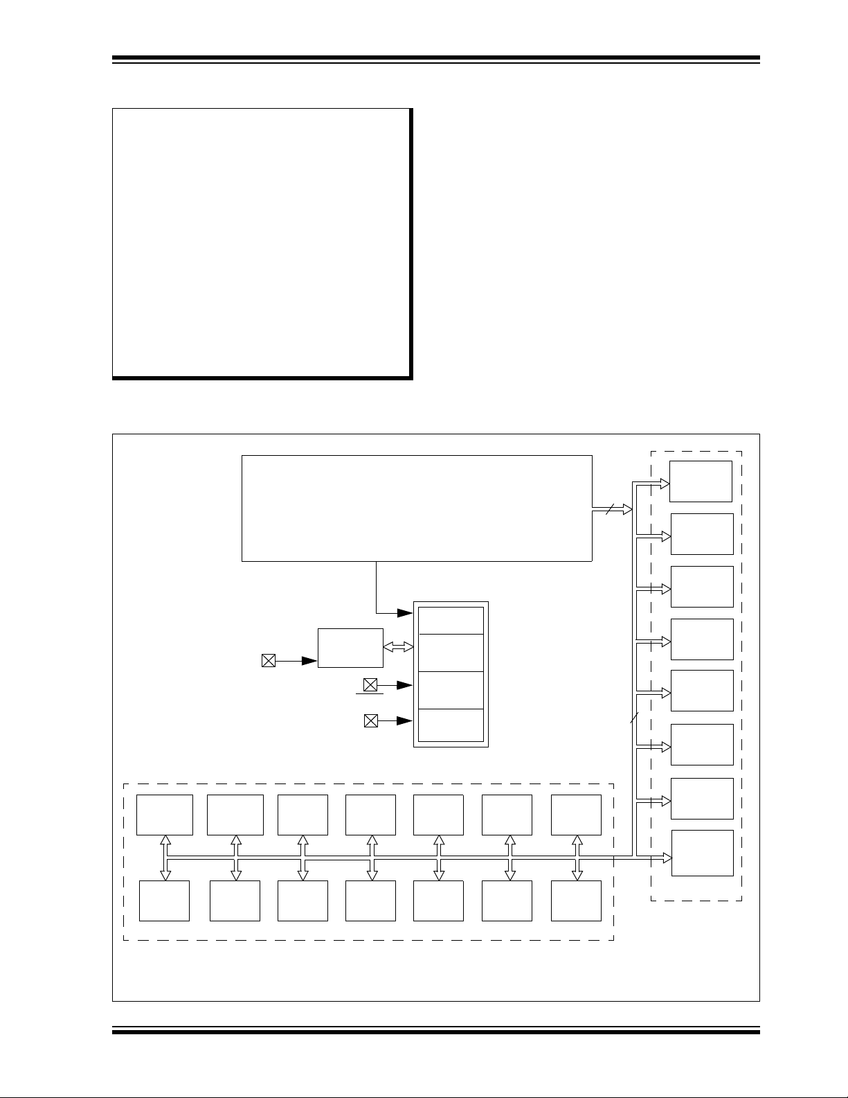
PORTA
Power-up
Timer
Oscillator
Start-up
OSC1/CLKI
MCLR
VDD, VSS
UART1,
Timing
Generation
ECAN1
(2)
I2C1,
ADC
Timers
Input
Capture
Output
Compare
AV
DD, AVSS
UART2
SPI2
SPI1,
Watchdog
Timer
POR/BOR
CRC
I2C2
QEI1
(1)
PWM
(1)
Remappable
Pins
Note 1: This feature or peripheral is only available on dsPIC33EPXXXMC20X/50X and PIC24EPXXXMC20X devices.
2: This feature or peripheral is only available on dsPIC33EPXXXGP/MC50X devices.
Op amp/
Comparator
CTMU
PTG
CPU
Refer to Figure 3-1 for CPU diagram details.
16
16
PORTA
PORTC
PORTD
PORTE
PORTF
PORTG
PORTS
Peripheral Modules
Timer
1.0 DEVICE OVERVIEW
This document contains device-specific information for
the dsPIC33EPXXXGP50X, dsPIC33EPXXXMC20X/
Note 1: This data sheet summarizes the fea-
tures of the dsPIC33EPXXXGP50X,
dsPIC33EPXXXMC20X/50X, and
PIC24EPXXXGP/MC20X families of
devices. It is not intended to be a comprehensive resource. To complement
the information in this data sheet, refer
to the related section of the “dsPIC33E/
PIC24E Family Reference Manual”,
which is available from the Microchip
50X, and PIC24EPXXXGP/MC20X Digital Signal
Controller (DSC) and Microcontroller (MCU) devices.
dsPIC33EPXXXMC20X/50X and dsPIC33EPXXXGP50X
devices contain extensive Digital Signal Processor (DSP)
functionality with a high-performance 16-bit MCU
architecture.
Figure 1-1 shows a general block diagram of the core
and peripheral modules. Ta b le 1- 1 lists the functions of
the various pins shown in the pinout diagrams.
web site (www.microchip.com)
2: Some registers and associated bits
described in this section may not be
available on all devices. Refer to
Section 4.0 “Memory Organization” in
this data sheet for device-specific register
and bit information.
FIGURE 1-1: dsPIC33EPXXXGP50X, dsPIC33EPXXXMC20X/50X, AND PIC24EPXXXGP/MC20X
BLOCK DIAGRAM
© 2011-2012 Microchip Technology Inc. Preliminary DS70657E-page 23

dsPIC33EPXXXGP50X, dsPIC33EPXXXMC20X/50X, AND PIC24EPXXXGP/MC20X
TABLE 1-1: PINOUT I/O DESCRIPTIONS
Pin
Pin Name
AN0-AN15 I Analog No Analog input channels.
CLKI
CLKO
OSC1
OSC2
REFCLKO O — Yes Reference clock output.
IC1-IC4 I ST Yes Capture inputs 1 through 4.
OCFA
OCFB
OC1-OC4
INT0
INT1
INT2
RA0-RA4, RA7-RA12 I/O ST No PORTA is a bidirectional I/O port.
RB0-RB15 I/O ST No PORTB is a bidirectional I/O port.
RC0-RC13, RC15 I/O ST No PORTC is a bidirectional I/O port.
RD5, RD6, RD8 I/O ST No PORTD is a bidirectional I/O port.
RE12-RE15 I/O ST No PORTE is a bidirectional I/O port.
RF0, RF1 I/O ST No PORTF is a bidirectional I/O port.
RG6-RG9 I/O ST No PORTG is a bidirectional I/O port.
T1CK
T2CK
T3CK
T4CK
T5CK
CTPLS
CTED1
CTED2
U1CTS
U1RTS
U1RX
U1TX
BCLK1
Legend: CMOS = CMOS compatible input or output Analog = Analog input P = Power
Note 1: This pin is available on dsPIC33EPXXXMC20X/50X and PIC24EPXXXMC20X devices only.
2: This pin is available on dsPIC33EPXXXGP/MC50X devices only.
3: This is the default Fault on Reset for dsPIC33EPXXXMC20X/50X and PIC24EPXXXMC20X devices. See
4: Not all pins are available in all packages variants. See the “Pin Diagrams” section for pin availability.
(4)
ST = Schmitt Trigger input with CMOS levels O = Output I = Input
PPS = Peripheral Pin Select TTL = TTL input buffer
Section 16.0 “High-Speed PWM Module (dsPIC33EPXXXMC20X/50X and PIC24EPXXXMC20X
Devices Only)” for more information.
Typ e
I
O
I
I/O
I
I
O
I
I
I
I
I
I
I
I
O
I
I
I
O
I
O
O
Buffer
Type
ST/
CMOS
—
ST/
CMOS
—
ST
ST
—
ST
ST
ST
ST
ST
ST
ST
ST
ST
ST
ST
ST
—
ST
—
ST
PPS Description
NoNoExternal clock source input. Always associated with OSC1 pin function.
Oscillator crystal output. Connects to crystal or resonator in Crystal
Oscillator mode. Optionally functions as CLKO in RC and EC modes.
Always associated with OSC2 pin function.
NoNoOscillator crystal input. ST buffer when configured in RC mode; CMOS
otherwise.
Oscillator crystal output. Connects to crystal or resonator in Crystal
Oscillator mode. Optionally functions as CLKO in RC and EC modes.
Yes
Compare Fault A input (for Compare channels).
No
Compare Fault B input (for Compare channels).
Yes
Compare outputs 1 through 4.
No
External interrupt 0.
Yes
External interrupt 1.
Yes
External interrupt 2.
No
Timer1 external clock input.
Yes
Timer2 external clock input.
No
Timer3 external clock input.
No
Timer4 external clock input.
No
Timer5 external clock input.
No
CTMU pulse output.
No
CTMU external edge input 1.
No
CTMU external edge input 2.
No
UART1 clear to send.
No
UART1 ready to send.
Yes
UART1 receive.
Yes
UART1 transmit.
No
UART1 IrDA baud clock output.
DS70657E-page 24 Preliminary © 2011-2012 Microchip Technology Inc.
dsPIC33EPXXXGP50X, dsPIC33EPXXXMC20X/50X, AND PIC24EPXXXGP/MC20X
TABLE 1-1: PINOUT I/O DESCRIPTIONS (CONTINUED)
Pin
Pin Name
(4)
Typ e
Buffer
Type
PPS Description
U2CTS
U2RTS
U2RX
U2TX
BCLK2
SCK1
SDI1
SDO1
SS1
SCK2
SDI2
SDO2
SS2
SCL1
SDA1
ASCL1
ASDA1
SCL2
SDA2
ASCL2
ASDA2
TMS
TCK
TDI
TDO
(2)
(2)
(1)
, FLT2
(1)
, FLT4
(1,3)
(1)
(1)
(1)
(1)
(1)
(1)
(1)
(1)
(1)
(1)
C1RX
C1TX
FLT1
FLT3
FLT32
DTCMP1-DTCMP3
PWM1L-PWM3L
PWM1H-PWM3H
SYNCI1
SYNCO1
INDX1
HOME1
QEA1
QEB1
CNTCMP1
(1)
(1)
O
O
O
I/O
O
I/O
I/O
O
I/O
I/O
I/O
I/O
I/O
I/O
I/O
I/O
I/O
O
O
O
O
O
O
I
I
I
I
I
I
I
I
I
I
I
I
I
I
I
I
I
ST
ST
ST
ST
ST
ST
ST
ST
ST
ST
ST
ST
ST
ST
ST
ST
ST
ST
ST
ST
—
—
—
—
—
No
No
Yes
Yes
No
No
No
No
No
Yes
Yes
Yes
Yes
No
No
No
No
No
No
No
No
No
No
No
No
ST—Yes
Yes
ST
Yes
ST
ST
ST
ST
ST
ST
ST
ST
—
—
—
—
No
No
Yes
No
No
Yes
Yes
Yes
Yes
Yes
Yes
Yes
UART2 clear to send.
UART2 ready to send.
UART2 receive.
UART2 transmit.
UART2 IrDA baud clock output.
Synchronous serial clock input/output for SPI1.
SPI1 data in.
SPI1 data out.
SPI1 slave synchronization or frame pulse I/O.
Synchronous serial clock input/output for SPI2.
SPI2 data in.
SPI2 data out.
SPI2 slave synchronization or frame pulse I/O.
Synchronous serial clock input/output for I2C1.
Synchronous serial data input/output for I2C1.
Alternate synchronous serial clock input/output for I2C1.
Alternate synchronous serial data input/output for I2C1.
Synchronous serial clock input/output for I2C2.
Synchronous serial data input/output for I2C2.
Alternate synchronous serial clock input/output for I2C2.
Alternate synchronous serial data input/output for I2C2.
JTAG Test mode select pin.
JTAG test clock input pin.
JTAG test data input pin.
JTAG test data output pin.
ECAN1 bus receive pin.
ECAN1 bus transmit pin.
PWM Fault input 1 and 2.
PWM Fault input 3 and 4.
PWM Fault input 32 (Class B Fault).
PWM Dead Time Compensation Input 1 through 3.
PWM Low Output 1 through 3.
PWM High Output 1 through 3.
PWM Synchronization Input 1.
PWM Synchronization Output 1.
Quadrature Encoder Index1 Pulse input.
Quadrature Encoder Home1 Pulse input.
Quadrature Encoder Phase A input in QEI1 mode. Auxiliary Timer
External Clock/Gate input in Timer mode.
Quadrature Encoder Phase B input in QEI1 mode. Auxiliary Timer
External Clock/Gate input in Timer mode.
Quadrature Encoder Compare Output 1.
Legend: CMOS = CMOS compatible input or output Analog = Analog input P = Power
ST = Schmitt Trigger input with CMOS levels O = Output I = Input
PPS = Peripheral Pin Select TTL = TTL input buffer
Note 1: This pin is available on dsPIC33EPXXXMC20X/50X and PIC24EPXXXMC20X devices only.
2: This pin is available on dsPIC33EPXXXGP/MC50X devices only.
3: This is the default Fault on Reset for dsPIC33EPXXXMC20X/50X and PIC24EPXXXMC20X devices. See
Section 16.0 “High-Speed PWM Module (dsPIC33EPXXXMC20X/50X and PIC24EPXXXMC20X
Devices Only)” for more information.
4: Not all pins are available in all packages variants. See the “Pin Diagrams” section for pin availability.
© 2011-2012 Microchip Technology Inc. Preliminary DS70657E-page 25
dsPIC33EPXXXGP50X, dsPIC33EPXXXMC20X/50X, AND PIC24EPXXXGP/MC20X
TABLE 1-1: PINOUT I/O DESCRIPTIONS (CONTINUED)
Pin
Pin Name
(4)
C1IN1C1IN2C1IN1+
OA1OUT
C1OUT
C2IN1C2IN2C2IN1+
OA2OUT
C2OUT
C3IN1C3IN2C3IN1+
OA3OUT
C3OUT
C4IN1C4IN1+
C4OUT
REF1O
CV
CVREF2O
PGED1
PGEC1
PGED2
PGEC2
PGED3
PGEC3
MCLR
AVDD P P No Positive supply for analog modules. This pin must be connected at all
AV
SS P P No Ground reference for analog modules. This pin must be connected at all
DD P — No Positive supply for peripheral logic and I/O pins.
V
V
CAP P — No CPU logic filter capacitor connection.
V
SS P — No Ground reference for logic and I/O pins.
V
REF+ I Analog No Analog voltage reference (high) input.
V
REF- I Analog No Analog voltage reference (low) input.
Legend: CMOS = CMOS compatible input or output Analog = Analog input P = Power
ST = Schmitt Trigger input with CMOS levels O = Output I = Input
PPS = Peripheral Pin Select TTL = TTL input buffer
Note 1: This pin is available on dsPIC33EPXXXMC20X/50X and PIC24EPXXXMC20X devices only.
2: This pin is available on dsPIC33EPXXXGP/MC50X devices only.
3: This is the default Fault on Reset for dsPIC33EPXXXMC20X/50X and PIC24EPXXXMC20X devices. See
Section 16.0 “High-Speed PWM Module (dsPIC33EPXXXMC20X/50X and PIC24EPXXXMC20X
Devices Only)” for more information.
4: Not all pins are available in all packages variants. See the “Pin Diagrams” section for pin availability.
Buffer
Typ e
I
Analog
I
Analog
I
Analog
O
Analog
O
I
Analog
I
Analog
I
Analog
O
Analog
O
I
Analog
I
Analog
I
Analog
O
Analog
O
I
Analog
I
Analog
O
OOAnalog
AnalogNoNo
I/O
I
I/O
I
I/O
I
Type
PPS Description
No
Op amp/Comparator 1 Negative Input 1.
No
Comparator 1 Negative Input 2.
No
Op amp/Comparator 1 Positive Input 1.
No
Op amp 1 Output.
—
Yes
Comparator 1 Output.
No
Op amp/Comparator 2 Negative Input 1.
No
Comparator 2 Negative Input 2.
No
Op amp/Comparator 2 Positive Input 1.
No
Op amp 2 Output.
—
Yes
Comparator 2 Output.
No
Op amp/Comparator 3 Negative Input 1.
No
Comparator 3 Negative Input 2.
No
Op amp/Comparator 3 Positive Input 1.
No
Op amp 3 Output.
—
Yes
Comparator 3 Output.
No
Comparator 4 Negative Input 1.
No
Comparator 4 Positive Input 1.
—
Yes
Comparator 4 Output.
Op amp/Comparator Voltage Reference Output.
Op amp/Comparator Voltage Reference divided by 2 Output.
ST
ST
ST
ST
ST
ST
No
Data I/O pin for programming/debugging communication channel 1.
No
Clock input pin for programming/debugging communication channel 1.
No
Data I/O pin for programming/debugging communication channel 2.
No
Clock input pin for programming/debugging communication channel 2.
No
Data I/O pin for programming/debugging communication channel 3.
No
Clock input pin for programming/debugging communication channel 3.
I/P ST No Master Clear (Reset) input. This pin is an active-low Reset to the
device.
times.
times.
DS70657E-page 26 Preliminary © 2011-2012 Microchip Technology Inc.

dsPIC33EPXXXGP50X, dsPIC33EPXXXMC20X/50X, AND PIC24EPXXXGP/MC20X
2.0 GUIDELINES FOR GETTING STARTED WITH 16-BIT DIGITAL SIGNAL CONTROLLERS AND MICROCONTROLLERS
Note 1: This data sheet summarizes the features
of the dsPIC33EPXXXGP50X,
dsPIC33EPXXXMC20X/50X, and
PIC24EPXXXGP/MC20X families of
devices. It is not intended to be a comprehensive reference source. To complement the information in this data sheet,
refer to the related section of the
“dsPIC33E/PIC24E Family Reference
Manual”, which is available from the
Microchip web site (www.microchip.com)
2: Some registers and associated bits
described in this section may not be
available on all devices. Refer to
Section 4.0 “Memory Organization” in
this data sheet for device-specific register
and bit information.
2.1 Basic Connection Requirements
Getting started with the dsPIC33EPXXXGP50X,
dsPIC33EPXXXMC20X/50X, and
PIC24EPXXXGP/MC20X families requires attention to a
minimal set of device pin connections before proceeding
with development. The following is a list of pin names,
which must always be connected:
DD and VSS pins
• All V
(see Section 2.2 “Decoupling Capacitors”)
• All AV
•V
•MCLR
• PGECx/PGEDx pins used for In-Circuit Serial
• OSC1 and OSC2 pins when external oscillator
Additionally, the following pins may be required:
•V
DD and AVSS pins (regardless if ADC module
is not used)
(see Section 2.2 “Decoupling Capacitors”)
CAP
(see Section 2.3 “CPU Logic Filter Capacitor
Connection (V
pin
(see Section 2.4 “Master Clear (MCLR) Pin”)
Programming™ (ICSP™) and debugging purposes
(see Section 2.5 “ICSP Pins”)
source is used
(see Section 2.6 “External Oscillator Pins”)
REF+/VREF- pins are used when external voltage
reference for ADC module is implemented
Note: The AV
CAP)”)
DD and AVSS pins must be
connected independent of the ADC
voltage reference source.
2.2 Decoupling Capacitors
The use of decoupling capacitors on every pair of
power supply pins, such as V
AVSS is required.
Consider the following criteria when using decoupling
capacitors:
• Value and type of capacitor: Recommendation
of 0.1 µF (100 nF), 10-20V. This capacitor should
be a low-ESR and have resonance frequency in
the range of 20 MHz and higher. It is
recommended to use ceramic capacitors.
• Placement on the printed circuit board: The
decoupling capacitors should be placed as close
to the pins as possible. It is recommended to
place the capacitors on the same side of the
board as the device. If space is constricted, the
capacitor can be placed on another layer on the
PCB using a via; however, ensure that the trace
length from the pin to the capacitor is within
one-quarter inch (6 mm) in length.
• Handling high frequency noise: If the board is
experiencing high frequency noise, above tens of
MHz, add a second ceramic-type capacitor in
parallel to the above described decoupling
capacitor. The value of the second capacitor can
be in the range of 0.01 µF to 0.001 µF. Place this
second capacitor next to the primary decoupling
capacitor. In high-speed circuit designs, consider
implementing a decade pair of capacitances as
close to the power and ground pins as possible.
For example, 0.1 µF in parallel with 0.001 µF.
• Maximizing performance: On the board layout
from the power supply circuit, run the power and
return traces to the decoupling capacitors first,
and then to the device pins. This ensures that the
decoupling capacitors are first in the power chain.
Equally important is to keep the trace length
between the capacitor and the power pins to a
minimum, thereby reducing PCB track
inductance.
DD, VSS, AVDD and
© 2011-2012 Microchip Technology Inc. Preliminary DS70657E-page 27
dsPIC33EPXXXGP50X, dsPIC33EPXXXMC20X/50X, AND PIC24EPXXXGP/MC20X
dsPIC33E/PIC24E
VDD
VSS
VDD
VSS
VSS
VDD
AVDD
AVSS
VDD
VSS
0.1 µF
Ceramic
0.1 µF
Ceramic
0.1 µF
Ceramic
0.1 µF
Ceramic
C
R
V
DD
MCLR
0.1 µF
Ceramic
VCAP
L1
(1)
R1
10 µF
Tantalum
Note 1: As an option, instead of a hard-wired connection, an
inductor (L1) can be substituted between V
DD and
AV
DD to improve ADC noise rejection. The inductor
impedance should be less than 1Ω and the inductor
capacity greater than 10 mA.
Where:
f
FCNV
2
--------------=
f
1
2π LC()
-----------------------=
L
1
2πfC()
---------------------
⎝⎠
⎛⎞
2
=
(i.e., ADC conversion rate/2)
Note 1: R ≤ 10 kΩ is recommended. A suggested
starting value is 10 kΩ. Ensure that the MCLR
pin VIH and VIL specifications are met.
2: R1 ≤ 470Ω will limit any current flowing into
MCLR
from the external capacitor C, in the
event of MCLR
pin breakdown, due to
Electrostatic Discharge (ESD) or Electrical
Overstress (EOS). Ensure that the MCLR
pin
V
IH and VIL specifications are met.
C
R1
(2)
R
(1)
VDD
MCLR
dsPIC33EP/PIC24EP
JP
FIGURE 2-1: RECOMMENDED
MINIMUM CONNECTION
The placement of this capacitor should be close to the
CAP pin. It is recommended that the trace length not
V
exceeds one-quarter inch (6 mm). See Section 27.3
“On-Chip Voltage Regulator” for details.
2.4 Master Clear (MCLR) Pin
The MCLR pin provides two specific device
functions:
• Device Reset
• Device Programming and Debugging.
During device programming and debugging, the
resistance and capacitance that can be added to the
pin must be considered. Device programmers and
debuggers drive the MCLR
specific voltage levels (VIH and VIL) and fast signal
transitions must not be adversely affected. Therefore,
specific values of R and C will need to be adjusted
based on the application and PCB requirements.
For example, as shown in Figure 2-2, it is
recommended that the capacitor C, be isolated from
the MCLR
pin during programming and debugging
operations.
Place the components as shown in Figure 2-2 within
one-quarter inch (6 mm) from the MCLR
pin. Consequently,
pin.
CAP)
2.2.1 TANK CAPACITORS
On boards with power traces running longer than six
inches in length, it is suggested to use a tank capacitor
for integrated circuits including DSCs to supply a local
power source. The value of the tank capacitor should
be determined based on the trace resistance that connects the power supply source to the device, and the
maximum current drawn by the device in the application. In other words, select the tank capacitor so that it
meets the acceptable voltage sag at the device. Typical
values range from 4.7 µF to 47 µF.
2.3 CPU Logic Filter Capacitor
A low-ESR (< 1 Ohms) capacitor is required on the
CAP pin, which is used to stabilize the voltage
V
regulator output voltage. The VCAP pin must not be
connected to VDD, and must have a capacitor greater
than 4.7 µF (10 µF is recommended), 16V connected
to ground. The type can be ceramic or tantalum. See
Section 30.0 “Electrical Characteristics” for
additional information.
DS70657E-page 28 Preliminary © 2011-2012 Microchip Technology Inc.
Connection (V
FIGURE 2-2: EXAMPLE OF MCLR PIN
CONNECTIONS
dsPIC33EPXXXGP50X, dsPIC33EPXXXMC20X/50X, AND PIC24EPXXXGP/MC20X
Main Oscillator
Guard Ring
Guard Trace
Oscillator Pins
2.5 ICSP Pins
The PGECx and PGEDx pins are used for ICSP and
debugging purposes. It is recommended to keep the
trace length between the ICSP connector and the ICSP
pins on the device as short as possible. If the ICSP connector is expected to experience an ESD event, a
series resistor is recommended, with the value in the
range of a few tens of Ohms, not to exceed 100 Ohms.
Pull-up resistors, series diodes and capacitors on the
PGECx and PGEDx pins are not recommended as they
will interfere with the programmer/debugger communications to the device. If such discrete components are
an application requirement, they should be removed
from the circuit during programming and debugging.
Alternatively, refer to the AC/DC characteristics and
timing requirements information in the respective
device Flash programming specification for information
on capacitive loading limits and pin input voltage high
IH) and input low (VIL) requirements.
(V
Ensure that the “Communication Channel Select” (i.e.,
PGECx/PGEDx pins) programmed into the device
matches the physical connections for the ICSP to
MPLAB
ICE™.
For more information on ICD 2, ICD 3 and REAL ICE
connection requirements, refer to the following
documents that are available on the Microchip web
site.
• “Using MPLAB
• “MPLAB
• “MPLAB
• “Using MPLAB
®
PICkit™ 3, MPLAB ICD 3, or MPLAB REAL
®
®
®
ICD 3” (poster) DS51765
ICD 3 Design Advisory” DS51764
REAL ICE™ In-Circuit Emulator User’s
Guide” DS51616
®
REAL ICE™ In-Circuit Emulator”
(poster) DS51749
2.6 External Oscillator Pins
Many DSCs have options for at least two oscillators: a
high-frequency primary oscillator and a low-frequency
secondary oscillator. For details, see Section 9.0
“Oscillator Configuration” for details.
The oscillator circuit should be placed on the same
side of the board as the device. Also, place the
oscillator circuit close to the respective oscillator pins,
not exceeding one-half inch (12 mm) distance
between them. The load capacitors should be placed
next to the oscillator itself, on the same side of the
board. Use a grounded copper pour around the
oscillator circuit to isolate them from surrounding
circuits. The grounded copper pour should be routed
directly to the MCU ground. Do not run any signal
traces or power traces inside the ground pour. Also, if
using a two-sided board, avoid any traces on the
other side of the board where the crystal is placed. A
suggested layout is shown in Figure 2-3.
FIGURE 2-3: SUGGESTED PLACEMENT
OF THE OSCILLATOR
CIRCUIT
© 2011-2012 Microchip Technology Inc. Preliminary DS70657E-page 29
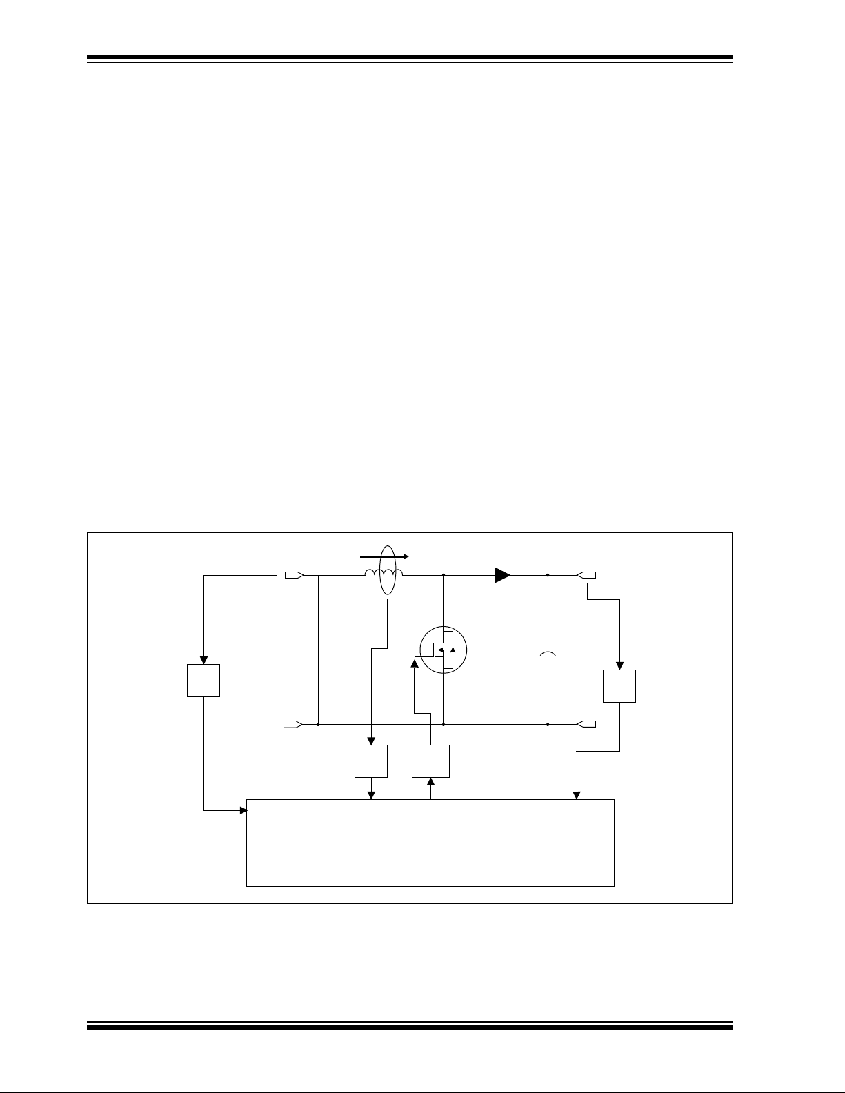
dsPIC33EPXXXGP50X, dsPIC33EPXXXMC20X/50X, AND PIC24EPXXXGP/MC20X
IPFC
VOUTPUT
ADC Channel
Op amp/
ADC Channel
PWM
k
1
k
2
k
3
FET
dsPIC33EP
VINPUT
Comparator Output
Driver
2.7 Oscillator Value Conditions on Device Start-up
If the PLL of the target device is enabled and
configured for the device start-up oscillator, the
maximum oscillator source frequency must be limited
to 3 MHz < F
IN < 5.5 MHz to comply with device PLL
start-up conditions. This means that if the external
oscillator frequency is outside this range, the
application must start-up in the FRC mode first. The
default PLL settings after a POR with an oscillator
frequency outside this range will violate the device
operating speed.
Once the device powers up, the application firmware
can initialize the PLL SFRs, CLKDIV and PLLDBF to a
suitable value, and then perform a clock switch to the
Oscillator + PLL clock source. Note that clock switching
must be enabled in the device Configuration Word.
2.8 Unused I/Os
Unused I/O pins should be configured as outputs and
driven to a logic-low state.
Alternatively, connect a 1k to 10k resistor between V
and unused pins and drive the output to logic low.
SS
2.9 Application Examples
• Induction heating
• Uninterruptable Power Supplies (UPS)
• DC/AC inverters
• Compressor motor control
• Washing machine 3-phase motor control
• BLDC motor control
• Automotive HVAC, cooling fans, fuel pumps
• Stepper motor control
• Audio and fluid sensor monitoring
• Camera lens focus and stability control
• Speech (playback, hands-free kits, answering
machines, VoIP)
• Consumer audio
• Industrial and building control (security systems
and access control)
• Barcode reading
• Networking: LAN switches, gateways
• Data storage device management
• Smart cards and smart card readers
Examples of typical application connections are shown
in Figure 2-4 through Figure 2-8.
FIGURE 2-4: BOOST CONVERTER IMPLEMENTATION
DS70657E-page 30 Preliminary © 2011-2012 Microchip Technology Inc.
 Loading...