

Datasheet dsPIC33EP256MU806, dsPIC33EP256MU810, dsPIC33EP256MU814, dsPIC33EP512GP806, dsPIC33EP512MC806 Datasheet
...Page 1

dsPIC33EPXXX(GP/MC/MU)806/810/814
and PIC24EPXXX(GP/GU)810/814
16-bit Microcontrollers and Digital Signal Controllers (up to 512 KB Flash
and 52 KB SRAM) with High-Speed PWM, USB, and Advanced Analog
Operating Conditions
• 3.0V to 3.6V, -40ºC to +125ºC, DC to 60 MIPS
• 3.0V to 3.6V, -40ºC to +85ºC, DC to 70 MIPS
Core: 16-bit dsPIC33E/PIC24E CPU
• Code-efficient (C and Assembly) architecture
• Two 40-bit wide accumulators
• Single-cycle (MAC/MPY) with dual data fetch
• Single-cycle mixed-sign MUL plus hardware divide
• 32-bit multiply support
Clock Management
• 2% internal oscillator
• Programmable PLLs and oscillator clock sources
• Fail-Safe Clock Monitor (FSCM)
• Independent Watchdog Timer
• Fast wake-up and start-up
Power Management
• Low-power management modes (Sleep, Idle, Doze)
• Integrated Power-on Reset and Brown-out Reset
• 1.0 mA/MHz dynamic current (typical)
•60 µA I
PD current (typical)
High-Speed PWM
• Up to seven PWM pairs with independent timing
• Dead Time for rising and falling edges
• 8.32 ns PWM resolution
• PWM support for:
- DC/DC, AC/DC, Inverters, PFC, Lighting
- BLDC, PMSM, ACIM, SRM
• Programmable Fault inputs
• Flexible trigger configurations for ADC conversions
Advanced Analog Features
• Two independent ADC modules:
- One ADC configurable as 10-bit, 1.1 Msps with four
S&H or 12-bit, 500 ksps with one S&H
- One 10-bit ADC, 1.1 Msps with four S&H
- Eight S&H using both ADC 10-bit modules
- 24 analog channels (64-pin devices) up to 32 analog
channels (100/121/144-pin devices)
• Flexible and independent ADC trigger sources
• Comparators:
- Up to three Analog Comparator modules
- Programmable references with 32 voltage points
Timers/Output Compare/Input Capture
• 27 General Purpose Timers:
- Nine 16-bit and up to four 32-bit Timers/Counters
- 16 OC modules configurable as Timers/Counters
- Two 32-bit Quadrature Encoder Interface (QEI)
modules configurable as Timers/Counters
• 16 IC modules
• Peripheral Pin Select (PPS) to allow function remap
• Real-Time Clock and Calendar (RTCC) module
Communication Interfaces
• USB 2.0 OTG-compliant full-speed interface
• Four UART modules (15 Mbps)
- Supports LIN 2.0 protocols and IrDA
• Four 4-wire SPI modules (15 Mbps)
• Two ECAN™ modules (1 Mbaud) CAN 2.0B support
2
•Two I
• Data Converter Interface (DCI) module with support for
• PPS to allow function remap
• Parallel Master Port (PMP)
• Programmable Cyclic Redundancy Check (CRC)
C modules (up to 1 Mbaud) with SMBus support
2
S and Audio codecs
I
®
Direct Memory Access (DMA)
• 15-channel DMA with user-selectable priority arbitration
• UART, USB, SPI, ADC, ECAN, IC, OC, Timers,
2
S, PMP
DCI/I
Input/Output
• Sink/Source 10 mA on all pins
• 5V-tolerant pins
• Selectable open drain, pull-ups, and pull-downs
• Up to 5 mA overvoltage clamp current
• External interrupts on all I/O pins
Qualification and Class B Support
• AEC-Q100 REVG (Grade 1 -40ºC to +125ºC) planned
• AEC-Q100 REVG (Grade 0 -40ºC to +150ºC) planned
• Class B Safety Library, IEC 60730
Debugger Development Support
• In-circuit and in-application programming
• Five program and three complex data breakpoints
• IEEE 1149.2-compatible (JTAG) boundary scan
• Trace and run-time watch
Packages
Type QFN TQFP TQFP TFBGA LQFP
Pin Count 64 64 144 100 121 144
I/O Pins (up to) 53 53 122 83 83 122
Contact/Lead Pitch 0.50 0.50 0.40 0.40 0.50 0.50 0.50
Dimensions 9x9x0.9 10x10x1 16x16x1 12x12x1 14x14x1 10x10x1.2 20x20x1.4
Note: All dimensions are in millimeters (mm) unless specified.
© 2009-2012 Microchip Technology Inc. Preliminary DS70616F-page 1
Page 2
dsPIC33EPXXX(GP/MC/MU)806/810/814 and PIC24EPXXX(GP/GU)810/814
dsPIC33EPXXX(GP/MC/MU)806/810/
814 and PIC24EPXXX(GP/GU)810/814
PRODUCT FAMILIES
The device names, pin counts, memory sizes and
peripheral availability of each device are listed in
Table 1. Their pinout diagrams appear on the following
pages.
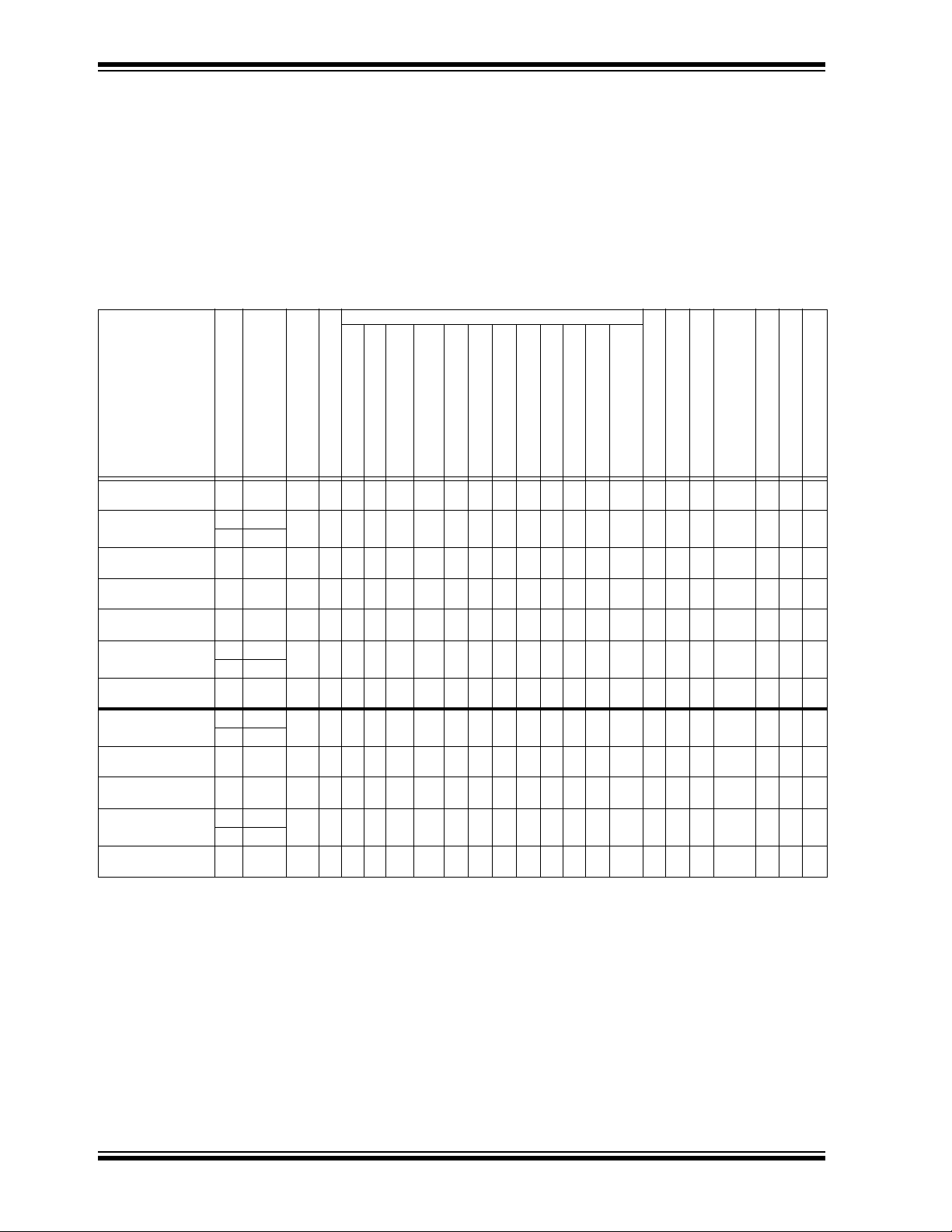
TABLE 1: dsPIC33EPXXX(GP/MC/MU)806/810/814 and PIC24EPXXX(GP/GU)810/814
CONTROLLER FAMILIES
Remappable Peripherals
(6)
SPI
ECAN™
External Interrupts
DMA Controller (Channels)
(2)
(3,4)
(1)
Device
dsPIC33EP256MU806 64
dsPIC33EP256MU810
dsPIC33EP256MU814 144
dsPIC33EP512GP806 64
dsPIC33EP512MC806 64
dsPIC33EP512MU810
dsPIC33EP512MU814 144
PIC24EP256GU810
PIC24EP256GU814 144
PIC24EP512GP806 64
PIC24EP512GU810
PIC24EP512GU814 144
Note 1: Flash size is inclusive of 24 Kbytes of auxiliary Flash. Auxiliary Flash supports simultaneous code execution and self-erase/programming.
Refer to Section 5. “Flash Programming” (DS70609) in the “dsPIC33E/PIC24E Family Reference Manual”.
2: RAM size is inclusive of 4 Kbytes of DMA RAM (DPSRAM) for all devices.
3: Up to eight of these timers can be combined into four 32-bit timers.
4: Eight out of nine timers are remappable.
5: PWM faults and Sync signals are remappable.
6: Four out of five interrupts are remappable.
7: Comparator output is remappable.
8: The ADC2 module supports 10-bit mode only.
Pins
Packages
QFN,
TQFP
100 TQFP
121 TFBGA
TQFP,
LQFP
QFN,
TQFP
QFN,
TQFP
100 TQFP
121 TFBGA
TQFP,
LQFP
100 TQFP
121 TFBGA
TQFP,
LQFP
QFN,
TQFP
100 TQFP
121 TFBGA
TQFP,L
QFP
(Kbyte)
RAM (Kbyte)
Input Capture
Program Flash Memory
16-bit Timer
280 28 9 16 16 8 2 4 4 2 5 15 1 3/4 1 2 1
280 28 9 16 16 12 2 4 4 2 5 15 1 3/4 1 2 1
280 28 9 16 16 14 2 4 4 2 5 15 1 3/4 1 2 1
536 52 9 16 16 — — 4 4 2 5 15 1 3/4 1 2 1
536 52 9 16 16 8 2 4 4 2 5 15 1 3/4 1 2 1
536 52 9 16 16 12 2 4 4 2 5 15 1 3/4 1 2 1
536 52 9 16 16 14 2 4 4 2 5 15 1 3/4 1 2 1
280 28 9 16 16 0 0 4 4 2 5 15 1 3/4 1 2 1
280 28 9 16 16 0 0 4 4 2 5 15 1 3/4 1 2 1
586 52 9 16 16 — — 4 4 2 5 15 1 3/4 1 2 1
536 52 9 16 16 0 0 4 4 2 5 15 1 3/4 1 2 1
536 52 9 16 16 0 0 4 4 2 5 15 1 3/4 1 2 1
Motor Control PWM
Output Compare (with PWM)
(5)
QEI
(Channels)
®
UART with IrDA
(7)
C™
2
I
DCI
RTCC
Analog Comparators/
Inputs Per Comparator
CRC Generator
(8)
10-bit/12-bit ADC
2 ADC,
24 ch
2 ADC,
32 ch
2 ADC,
32 ch
2 ADC,
24 ch
2 ADC,
24 ch
2 ADC,
32 ch
2 ADC,
32 ch
2 ADC,
32 ch
2 ADC,
32 ch
2 ADC,
24 ch
2 ADC,
32 ch
2 ADC,
32 ch
USB
Parallel Master Port
1Y51
1Y83
1Y122
—Y53
—Y53
1Y83
1Y122
1Y83
1Y122
—Y53
1Y83
1Y122
I/O Pins
DS70616F-page 2 Preliminary © 2009-2012 Microchip Technology Inc.
Page 3
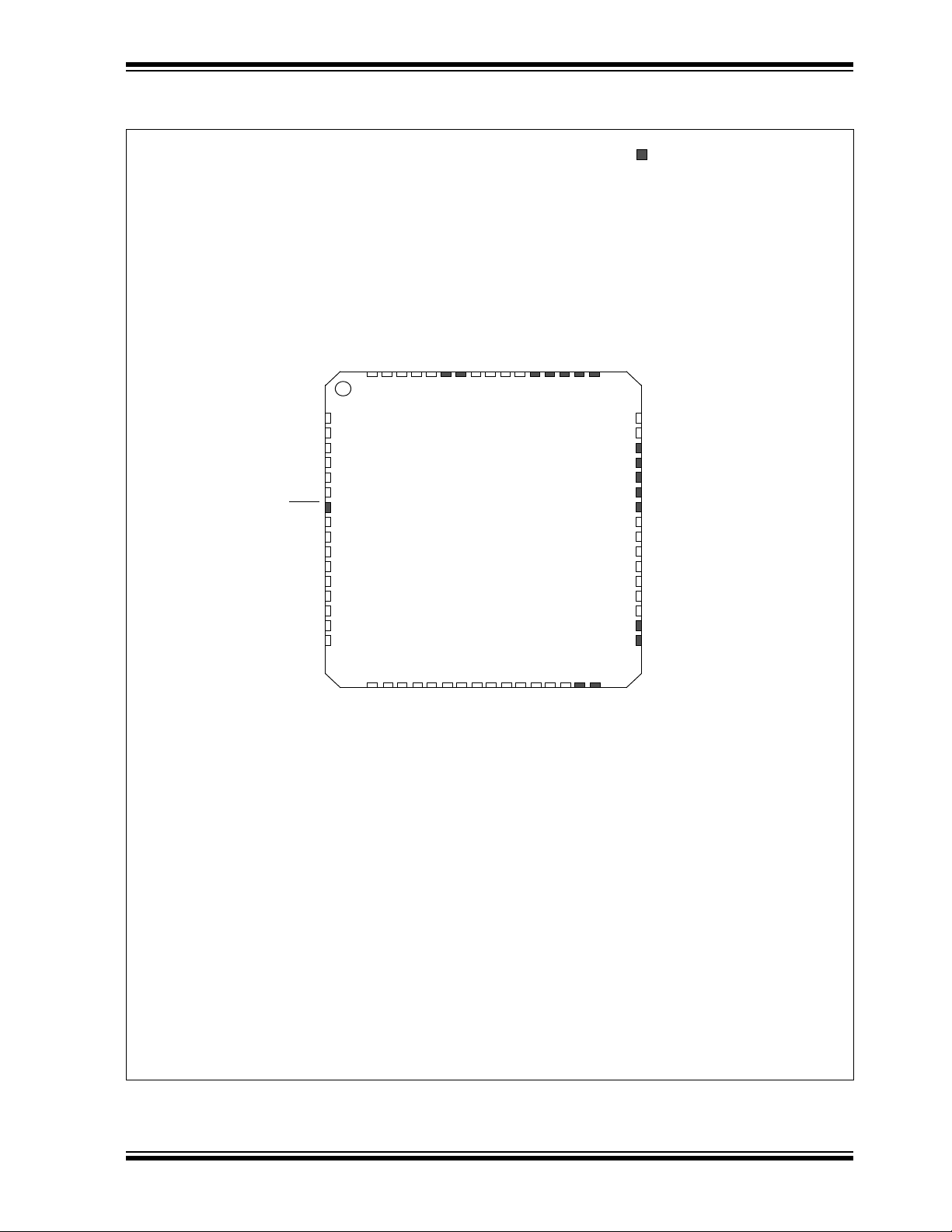
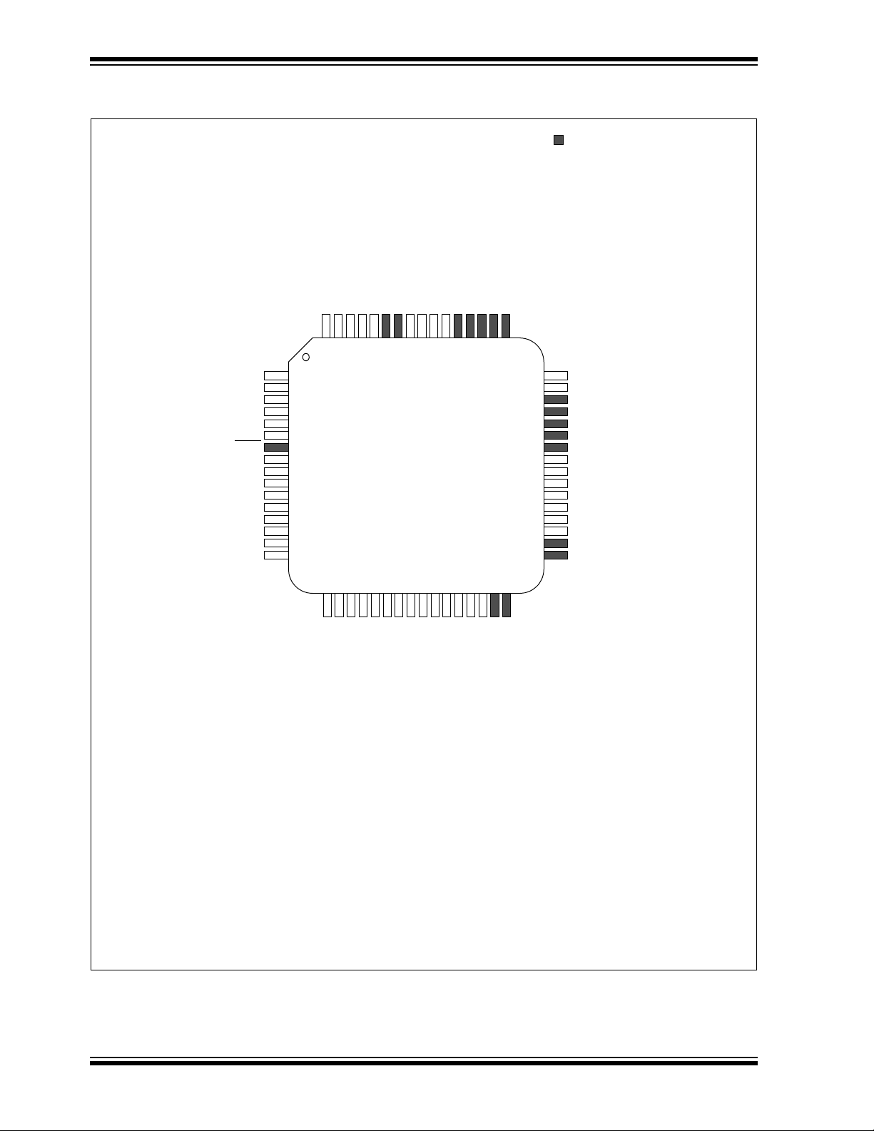
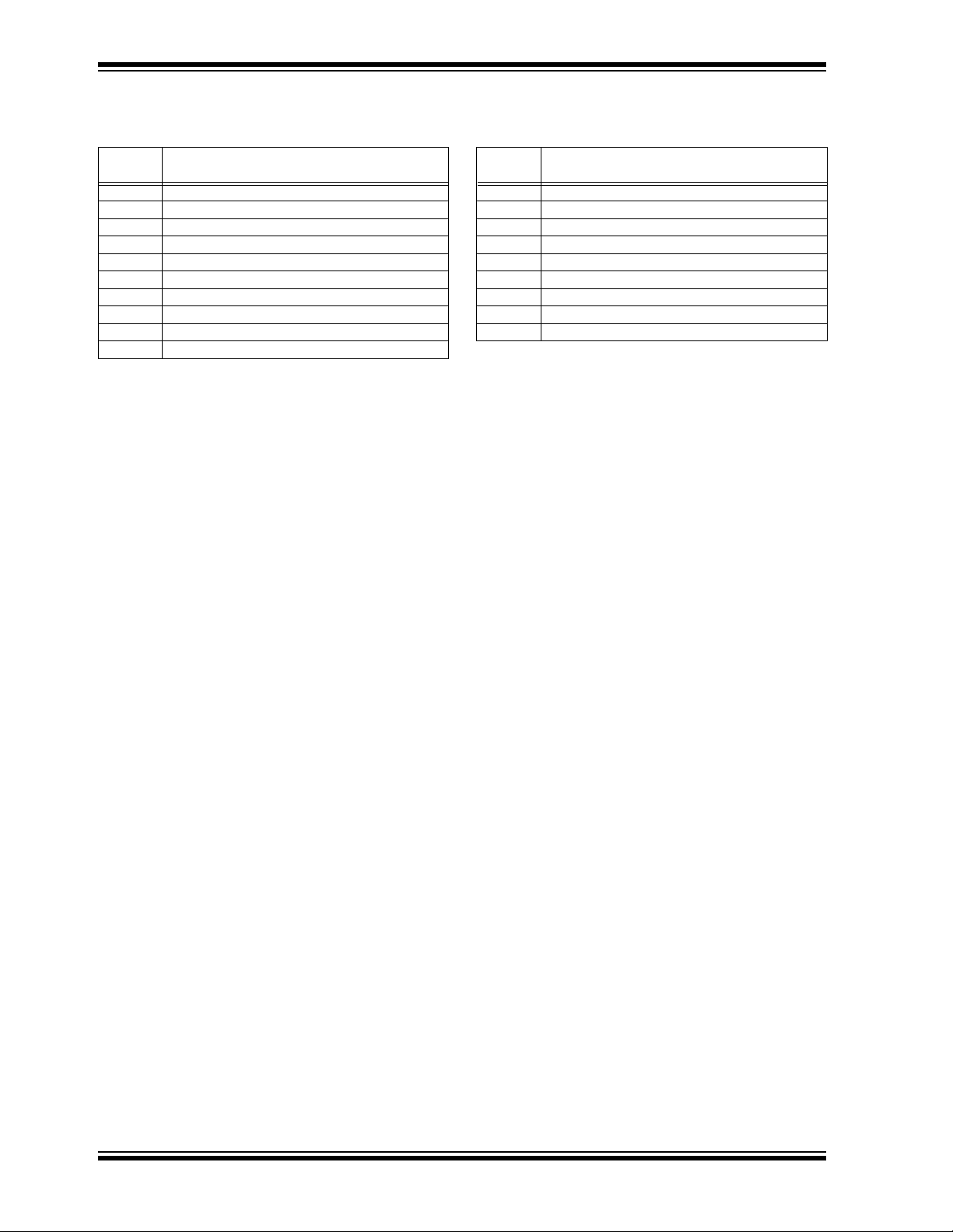
dsPIC33EPXXX(GP/MC/MU)806/810/814 and PIC24EPXXX(GP/GU)810/814
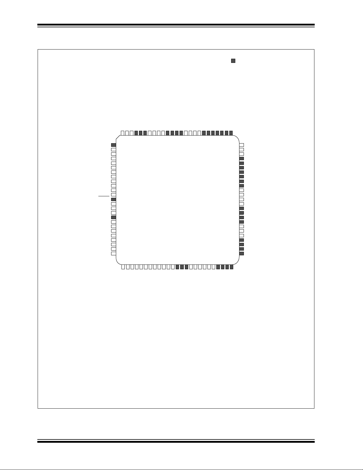
64-Pin QFN
Note 1: The RPn/RPIn pins can be used by any remappable peripheral with some limitation. See
Section 11.4 “Peripheral Pin Select” for available peripherals and for information on limitations.
2: Every I/O port pin (RAx-RGx) can be used as change notification (CNAx-CNGx). See Section 11.0
“I/O Ports” for more information.
3: The availability of I2C interfaces varies by device. Selection (SDAx/ SCLx or ASDAx/ASCLx) is made
using the device Configuration bits, ALTI2C1 and ALTI2C2 (FPOR<5:4>). See Section 29.0
“Special Features” for more information.
= Pins are up to 5V tolerant
48
49
1
dsPIC33EP256MU806
32
2
3
4
5
6
7
8
9
10
11
12
13
14
15
16
50
51
52
53
54
55
56
57
58
59
60
61
62
63
64
47
46
45
44
43
42
41
40
39
38
37
36
35
34
33
31
30
29
28
27
26
25
24
23
22
21
20
19
18
17
AN29/PWM3H/PMD5/RP85/RE5
AN31/PWM4H/PMD7/RP87/RE7
C1IN3-/SCK2/PMA5/RP118/RG6
C1IN1-/SDI2/PMA4/RPI119/RG7
C2IN3-/SDO2/PMA3/RP120/RG8
MCLR
C2IN1-/PMA2/RPI121/RG9
V
DD
PGEC3/AN1/V
REF
-/RPI33/RB1
PGED3/AN0/V
REF
+/RPI32/RB0
V
SS
AN30/PWM4L/PMD6/RPI86/RE6
PGEC2/SOSCO/C3IN1-/T1CK/RPI62/RC14
PGED2/SOSCI/C3IN3-/RPI61/RC13
INT0/DMH/RP64/RD0
PMCS1/RPI75/RD11
ASCL1/PMCS2/RPI74/RD10
ASDA1/DPLN/RPI73/RD9
RTCC/DMLN/RPI72/RD8
V
SS
OSC2/CLKO/RC15
OSC1/RPI60/RC12
V
DD
USBID/RP99/RF3
AN28/PWM3L/PMD4/RP84/RE4
AN27/PWM2H/PMD3/RPI83/RE3
AN26/PWM2L/PMD2/RP82/RE2
AN25/PWM1H/PMD1/RPI81/RE1
AN24/PWM1L/PMD0/RP80/RE0
VCMPST2/
RP97/RF1
V
CMPST
1/RP96/RF0
V
DD
VCAP
C3IN1+/V
CMPST
3/RP71/RD7
C3IN2-/RP70/RD6
PMRD/RP69/RD5
PMWR/RP68/RD4
PMBE/RP67/RD3
DPH/RP66/RD2
V
CPCON/RP65/RD1
PGEC1/AN6/RPI38/RB6
PGED1/AN7/RCV/RPI39/RB7
AV
DD
AV
SS
AN8/PMA6/RPI40/RB8
AN9/PMA7//RPI41/RB9
TMS/AN10/CV
REF
/PMA13/RPI42/RB10
TDO/AN11/PMA12/RPI43/RB11
V
SS
VDD
TCK/AN12/PMA11/RPI44/RB12
TDI/AN13/PMA10/RPI45/RB13
AN14/PMA1/RPI46/RB14
AN15/PMA0/RPI47/RB15
SDA2/PMA9/RP100/RF4
SCL2/PMA8/RP101/RF5
D+/RG2
D-/RG3
V
USB3V
3
V
BUS
AN4/C1IN2-/USBOEN/RPI36/RB4
AN3/C2IN1+/VPIO/RPI35/RB3
AN2/C2IN2-/VMIO/RPI34/RB2
AN5/C1IN1+/VBUSON/VBUSST/RPI37/RB5
Pin Diagrams
© 2009-2012 Microchip Technology Inc. Preliminary DS70616F-page 3
Page 4
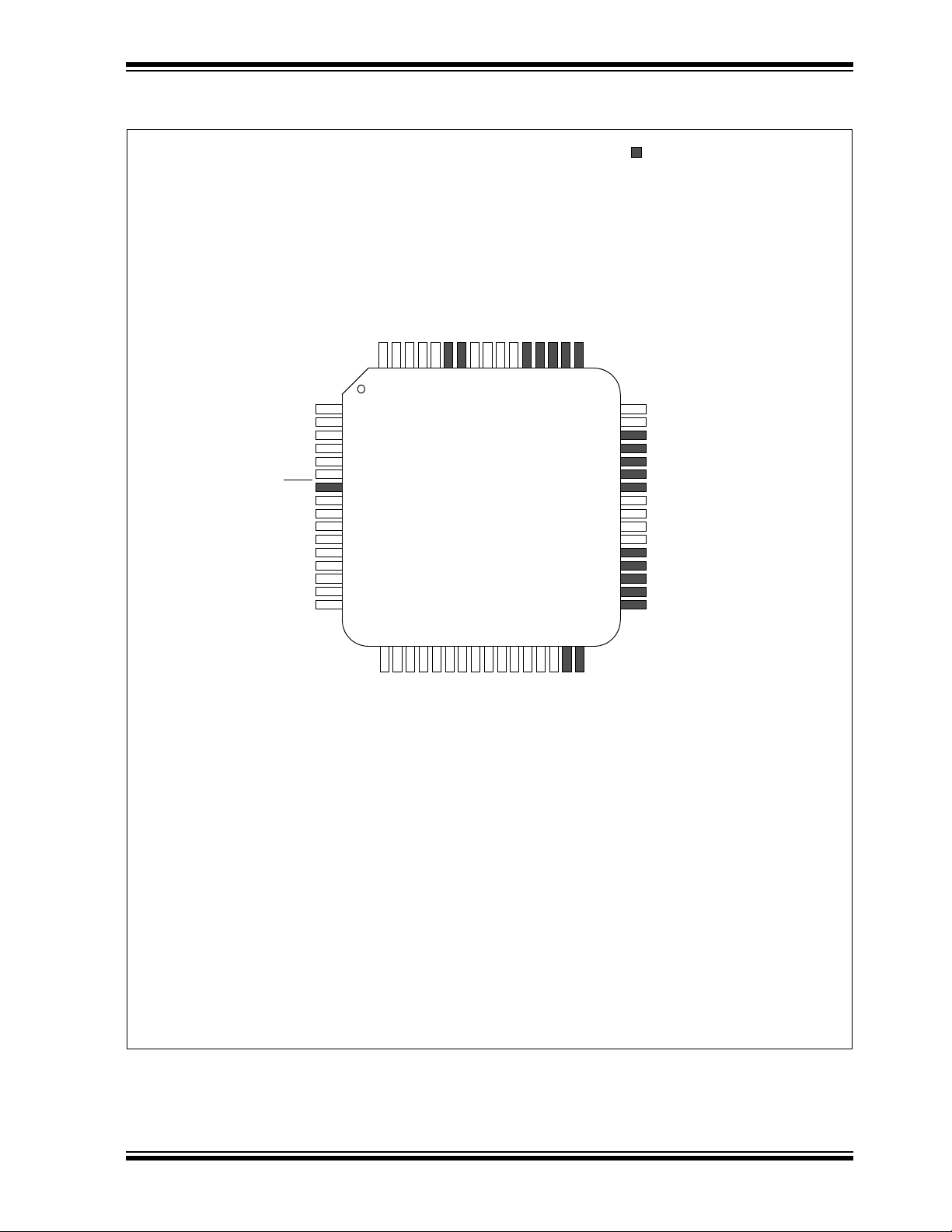
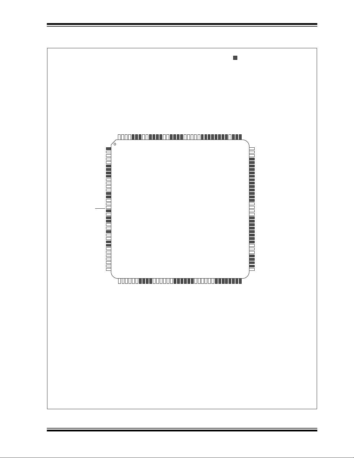
dsPIC33EPXXX(GP/MC/MU)806/810/814 and PIC24EPXXX(GP/GU)810/814
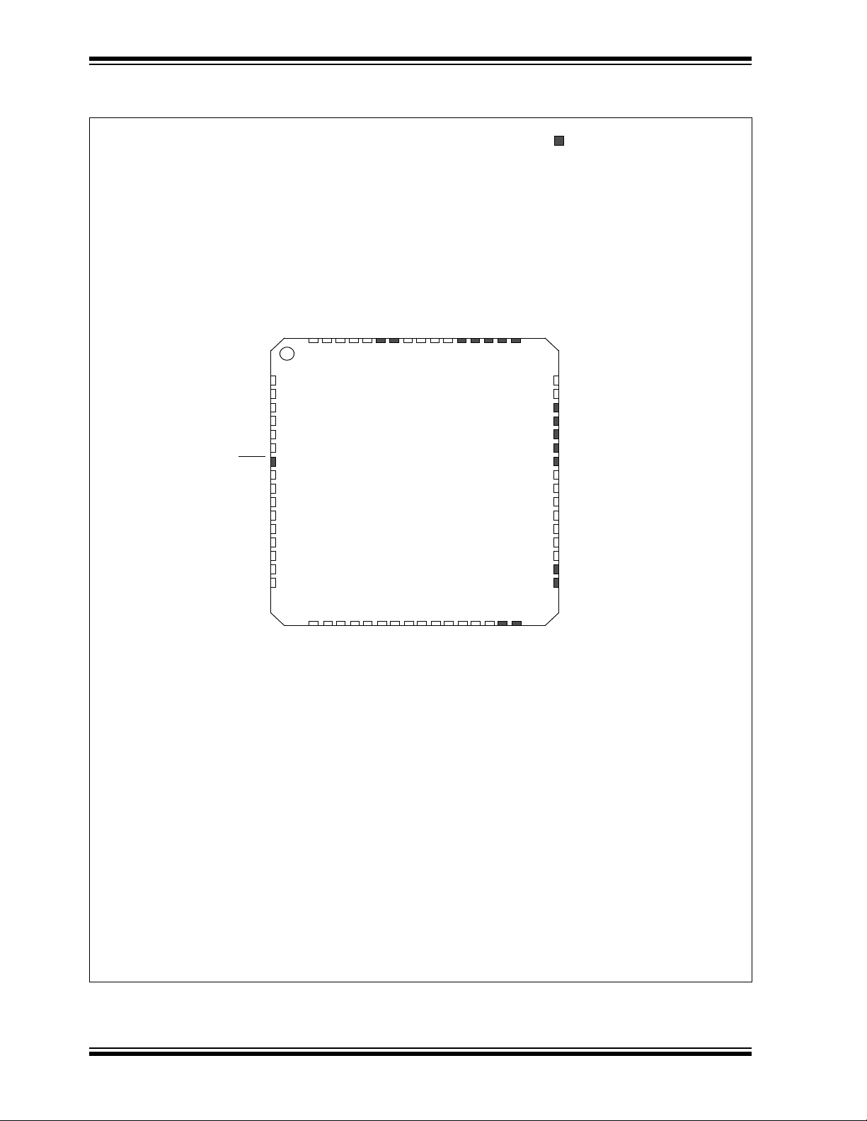
64-Pin QFN
Note 1: The RPn/RPIn pins can be used by any remappable peripheral with some limitation. See
Section 11.4 “Peripheral Pin Select” for available peripherals and for information on limitations.
2: Every I/O port pin (RAx-RGx) can be used as change notification (CNAx-CNGx). See Section 11.0
“I/O Ports” for more information.
3: The availability of I
2
C interfaces varies by device. Selection (SDAx/ SCLx or ASDAx/ASCLx) is made
using the device Configuration bits, ALTI2C1 and ALTI2C2 (FPOR<5:4>). See Section 29.0
“Special Features” for more information.
= Pins are up to 5V tolerant
48
49
1
dsPIC33EP512MC806
32
2
3
4
5
6
7
8
9
10
11
12
13
14
15
16
50
51
52
53
54
55
56
57
58
59
60
61
62
63
64
47
46
45
44
43
42
41
40
39
38
37
36
35
34
33
31
30
29
28
27
26
25
24
23
22
21
20
19
18
17
AN29/PWM3H/PMD5/RP85/RE5
AN31/PWM4H/PMD7/RP87/RE7
C1IN3-/SCK2/PMA5/RP118/RG6
C1IN1-/SDI2/PMA4/RPI119/RG7
C2IN3-/SDO2/PMA3/RP120/RG8
MCLR
C2IN1-/PMA2/RPI121/RG9
V
DD
PGEC3/AN1/V
REF
-/RPI33/RB1
PGED3/AN0/V
REF
+/RPI32/RB0
V
SS
AN30/PWM4L/PMD6/RPI86/RE6
PGEC2/SOSCO/C3IN1-/T1CK/RPI62/RC14
PGED2/SOSCI/C3IN3-/RPI61/RC13
INT0/RP64/RD0
PMCS1/RPI75/RD11
ASCL1/PMCS2/RPI74/RD10
ASDA1/RPI73/RD9
RTCC/RPI72/RD8
V
SS
OSC2/CLKO/RC15
OSC1/RPI60/RC12
V
DD
RP99/RF3
AN28/PWM3L/PMD4/RP84/RE4
AN27/PWM2H/PMD3/RPI83/RE3
AN26/PWM2L/PMD2/RP82/RE2
AN25/PWM1H/PMD1/RPI81/RE1
AN24/PWM1L/PMD0/RP80/RE0
RP97/RF1
RP96/RF0
VDDVCAP
C3IN1+/RP71/RD7
C3IN2-/RP70/RD6
PMRD/RP69/RD5
PMWR/RP68/RD4
PMBE/RP67/RD3
RP66/RD2
RP65/RD1
PGEC1/AN6/RPI38/RB6
PGED1/AN7/RPI39/RB7
AV
DD
AV
SS
AN8/PMA6/RPI40/RB8
AN9/PMA7//RPI41/RB9
TMS/AN10/CV
REF
/PMA13/RPI42/RB10
TDO/AN11/PMA12/RPI43/RB11
V
SS
VDD
TCK/AN12/PMA11/RPI44/RB12
TDI/AN13/PMA10/RPI45/RB13
AN14/PMA1/RPI46/RB14
AN15/PMA0/RPI47/RB15
SDA2/PMA9/RP100/RF4
SCL2/PMA8/RP101/RF5
SCLI/RG2
SDA1/RG3
RP102/RF6
RP98/RF2
AN5/C1IN1+/RPI37/RB5
AN4/C1IN2-/RPI36/RB4
AN3/C2IN1+/RPI35/RB3
AN2/C2IN2-/RPI34/RB2
Pin Diagrams
DS70616F-page 4 Preliminary © 2009-2012 Microchip Technology Inc.
Page 5
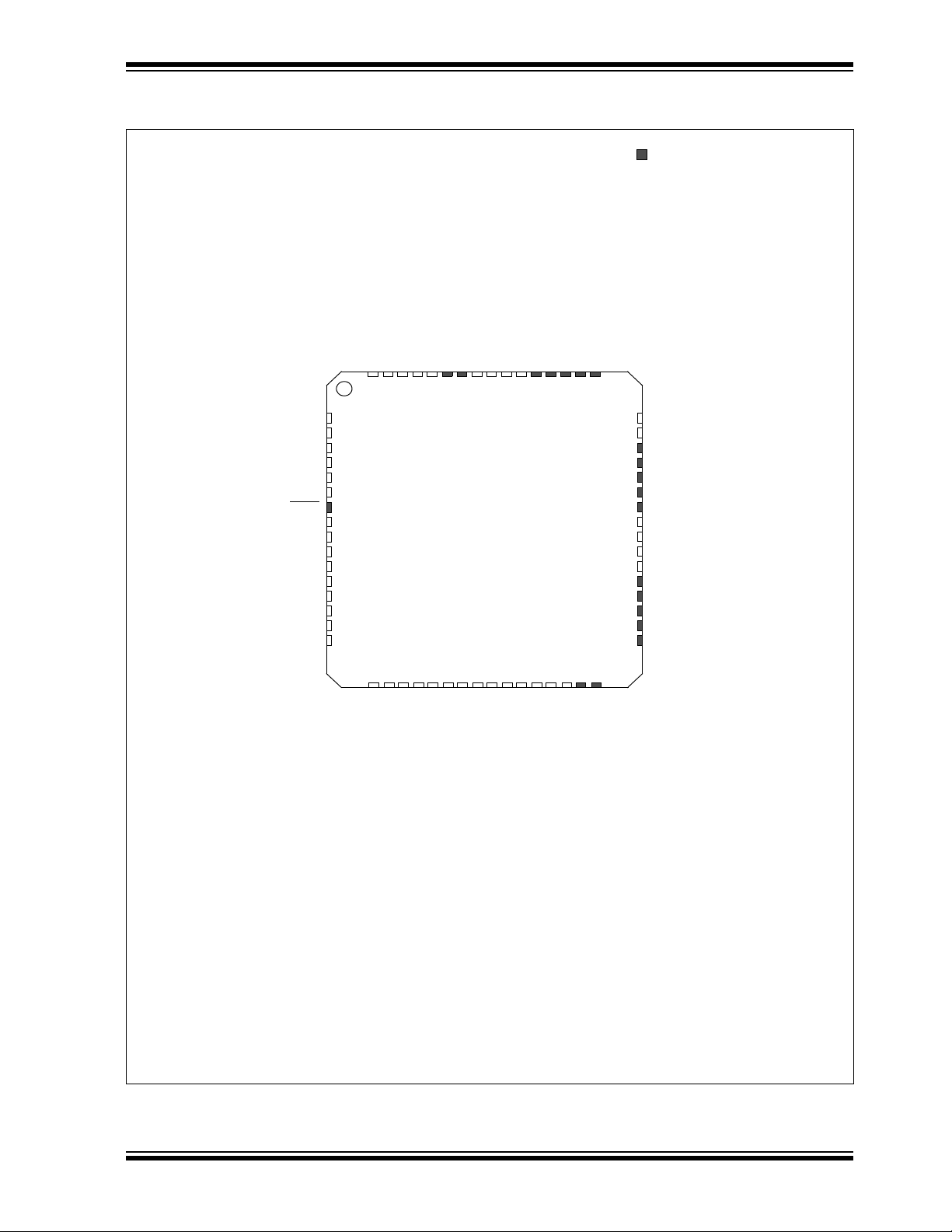
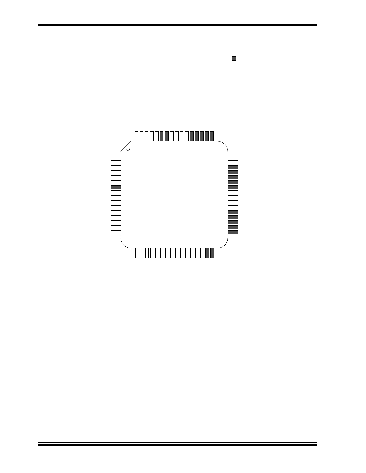
dsPIC33EPXXX(GP/MC/MU)806/810/814 and PIC24EPXXX(GP/GU)810/814
64-Pin QFN
Note 1: The RPn/RPIn pins can be used by any remappable peripheral with some limitation. See
Section 11.4 “Peripheral Pin Select” for available peripherals and for information on limitations.
2: Every I/O port pin (RAx-RGx) can be used as change notification (CNAx-CNGx). See Section 11.0
“I/O Ports” for more information.
3: The availability of I
2
C interfaces varies by device. Selection (SDAx/ SCLx or ASDAx/ASCLx) is made
using the device Configuration bits, ALTI2C1 and ALTI2C2 (FPOR<5:4>). See Section 29.0
“Special Features” for more information.
= Pins are up to 5V tolerant
48
49
1
dsPIC33EP512GP806
32
2
3
4
5
6
7
8
9
10
11
12
13
14
15
16
50
51
52
53
54
55
56
57
58
59
60
61
62
63
64
47
46
45
44
43
42
41
40
39
38
37
36
35
34
33
31
30
29
28
27
26
25
24
23
22
21
20
19
18
17
AN29/PMD5/RP85/RE5
AN31/PMD7/RP87/RE7
C1IN3-/SCK2/PMA5/RP118/RG6
C1IN1-/SDI2/PMA4/RPI119/RG7
C2IN3-/SDO2/PMA3/RP120/RG8
MCLR
C2IN1-/PMA2/RPI121/RG9
V
DD
PGEC3/AN1/V
REF
-/RPI33/RB1
PGED3/AN0/V
REF
+/RPI32/RB0
V
SS
AN30/PMD6/RPI86/RE6
PGEC2/SOSCO/C3IN1-/T1CK/RPI62/RC14
PGED2/SOSCI/C3IN3-/RPI61/RC13
INT0/RP64/RD0
PMCS1/RPI75/RD11
ASCL1/PMCS2/RPI74/RD10
ASDA1/RPI73/RD9
RTCC/RPI72/RD8
V
SS
OSC2/CLKO/RC15
OSC1/RPI60/RC12
V
DD
RP99/RF3
AN28/PMD4/RP84/RE4
AN27/PMD3/RPI83/RE3
AN26/PMD2/RP82/RE2
AN25/PMD1/RPI81/RE1
AN24/PMD0/RP80/RE0
RP97/RF1
RP96/RF0
VDDVCAP
C3IN1+/RP71/RD7
C3IN2-/RP70/RD6
PMRD/RP69/RD5
PMWR/RP68/RD4
PMBE/RP67/RD3
RP66/RD2
RP65/RD1
PGEC1/AN6/RPI38/RB6
PGED1/AN7/RPI39/RB7
AV
DD
AV
SS
AN8/PMA6/RPI40/RB8
AN9/PMA7//RPI41/RB9
TMS/AN10/CV
REF
/PMA13/RPI42/RB10
TDO/AN11/PMA12/RPI43/RB11
V
SS
VDD
TCK/AN12/PMA11/RPI44/RB12
TDI/AN13/PMA10/RPI45/RB13
AN14/PMA1/RPI46/RB14
AN15/PMA0/RPI47/RB15
SDA2/PMA9/RP100/RF4
SCL2/PMA8/RP101/RF5
SCLI/RG2
SDA1/RG3
RP102/RF6
RP98/RF2
AN5/C1IN1+/RPI37/RB5
AN4/C1IN2-/RPI36/RB4
AN3/C2IN1+/RPI35/RB3
AN2/C2IN2-/RPI34/RB2
PIC24EP512GP806
Pin Diagrams
© 2009-2012 Microchip Technology Inc. Preliminary DS70616F-page 5
Page 6
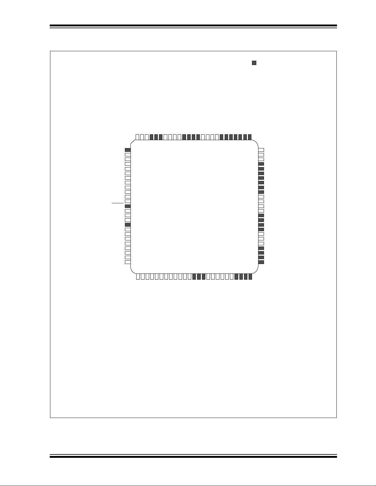
dsPIC33EPXXX(GP/MC/MU)806/810/814 and PIC24EPXXX(GP/GU)810/814
64-Pin TQFP
Note 1: The RPn/RPIn pins can be used by any remappable peripheral with some limitation. See
Section 11.4 “Peripheral Pin Select” for available peripherals and for information on limitations.
2: Every I/O port pin (RAx-RGx) can be used as change notification (CNAx-CNGx). See Section 11.0
“I/O Ports” for more information.
3: The availability of I
2
C interfaces varies by device. Selection (SDAx/ SCLx or ASDAx/ASCLx) is
made using the device Configuration bits, ALTI2C1 and ALTI2C2 (FPOR<5:4>). See Section 29.0
“Special Features” for more information.
= Pins are up to 5V tolerant
48
47
46
45
44
43
42
41
49
50
51
52
53
54
55
56
57
58
59
60
61
62
63
64
40
39
38
37
36
35
34
33
1
2
3
4
5
6
7
8
9
10
11
12
13
14
15
16
31
30
29
28
27
26
25
24
23
22
21
20
19
18
17
dsPIC33EP256MU806
32
AN29/PWM3H/PMD5/RP85/RE5
AN31/PWM4H/PMD7/RP87/RE7
C1IN3-/SCK2/PMA5/RP118/RG6
C1IN1-/SDI2/PMA4/RPI119/RG7
C2IN3-/SDO2/PMA3/RP120/RG8
MCLR
C2IN1-/PMA2/RPI121/RG9
V
DD
AN5/C1IN1+/V
BUSON/VBUSST
/RPI37/RB5
AN4/C1IN2-/USBOEN/RPI36/RB4
AN3/C2IN1+/VPIO/RPI35/RB3
AN2/C2IN2-/VMIO/RPI34/RB2
PGEC3/AN1/V
REF
-/RPI33/RB1
PGED3/AN0/V
REF
+/RPI32/RB0
V
SS
AN30/PWM4L/PMD6/RPI86/RE6
PGEC2/SOSCO/C3IN1-/T1CK/RPI62/RC14
PGED2/SOSCI/C3IN3-/RPI61/RC13
INT0/DMH/RP64/RD0
PMCS1/RPI75/RD11
ASCL1/PMCS2/RPI74/RD10
ASDA1/DPLN/RPI73/RD9
RTCC/DMLN/RPI72/RD8
V
SS
OSC2/CLKO/RC15
OSC1/RPI60/RC12
V
DD
USBID/RP99/RF3
AN28/PWM3L/PMD4/RP84/RE4
AN27/PWM2H/PMD3/RPI83/RE3
AN26/PWM2L/PMD2/RP82/RE2
AN25/PWM1H/PMD1/RPI81/RE1
AN24/PWM1L/PMD0/RP80/RE0
V
CMPST
2/RP97/RF1
V
CMPST
1/RP96/RF0
V
DDVCAP
C3IN1+/V
CMPST
3/RP71/RD7
C3IN2-/RP70/RD6
PMRD/RP69/RD5
PMWR/RP68/RD4
PMBE/RP67/RD3
DPH/RP66/RD2
V
CPCON
/RP65/RD1
PGEC1/AN6/RPI38/RB6
PGED1/AN7/RCV/RPI39/RB7
AV
DD
AV
SS
AN8/PMA6/RPI40/RB8
AN9/PMA7//RPI41/RB9
TMS/AN10/CV
REF
/PMA13/RPI42/RB10
TDO/AN11/PMA12/RPI43/RB11
V
SS
V
DD
TCK/AN12/PMA11/RPI44/RB12
TDI/AN13/PMA10/RPI45/RB13
AN14/PMA1/RPI46/RB14
AN15/PMA0/RPI47/RB15
SDA2/PMA9/RP100/RF4
SCL2/PMA8/RP101/RF5
D+/RG2
D-/RG3
V
USB3V
3
V
BUS
Pin Diagrams (Continued)
DS70616F-page 6 Preliminary © 2009-2012 Microchip Technology Inc.
Page 7
dsPIC33EPXXX(GP/MC/MU)806/810/814 and PIC24EPXXX(GP/GU)810/814
64-Pin TQFP
Note 1: The RPn/RPIn pins can be used by any remappable peripheral with some limitation. See
Section 11.4 “Peripheral Pin Select” for available peripherals and for information on limitations.
2: Every I/O port pin (RAx-RGx) can be used as change notification (CNAx-CNGx). See Section 11.0
“I/O Ports” for more information.
3: The availability of I
2
C interfaces varies by device. Selection (SDAx/ SCLx or ASDAx/ASCLx) is
made using the device Configuration bits, ALTI2C1 and ALTI2C2 (FPOR<5:4>). See Section 29.0
“Special Features” for more information.
= Pins are up to 5V tolerant
48
47
46
45
44
43
42
41
49
50
51
52
53
54
55
56
57
58
59
60
61
62
63
64
40
39
38
37
36
35
34
33
1
2
3
4
5
6
7
8
9
10
11
12
13
14
15
16
31
30
29
28
27
26
25
24
23
22
21
20
19
18
17
dsPIC33EP512GP806
32
AN29/PMD5/RP85/RE5
AN31/PMD7/RP87/RE7
C1IN3-/SCK2/PMA5/RP118/RG6
C1IN1-/SDI2/PMA4/RPI119/RG7
C2IN3-/SDO2/PMA3/RP120/RG8
MCLR
C2IN1-/PMA2/RPI121/RG9
V
DD
AN5/C1IN1+/RPI37/RB5
AN4/C1IN2-/RPI36/RB4
AN3/C2IN1+/RPI35/RB3
AN2/C2IN2-/RPI34/RB2
PGEC3/AN1/V
REF
-/RPI33/RB1
PGED3/AN0/V
REF
+/RPI32/RB0
V
SS
AN30/PMD6/RPI86/RE6
PGEC2/SOSCO/C3IN1-/T1CK/RPI62/RC14
PGED2/SOSCI/C3IN3-/RPI61/RC13
INT0/RP64/RD0
PMCS1/RPI75/RD11
ASCL1/PMCS2/RPI74/RD10
ASDA1/RPI73/RD9
RTCC/RPI72/RD8
V
SS
OSC2/CLKO/RC15
OSC1/RPI60/RC12
V
DD
RP99/RF3
AN28/PMD4/RP84/RE4
AN27/PMD3/RPI83/RE3
AN26/PMD2/RP82/RE2
AN25/PMD1/RPI81/RE1
AN24/PMD0/RP80/RE0
RP97/RF1
RP96/RF0
VDDV
CAP
C3IN1+/RP71/RD7
C3IN2-/RP70/RD6
PMRD/RP69/RD5
PMWR/RP68/RD4
PMBE/RP67/RD3
RP66/RD2
RP65/RD1
PGEC1/AN6/RPI38/RB6
PGED1/AN7/RPI39/RB7
AV
DD
AV
SS
AN8/PMA6/RPI40/RB8
AN9/PMA7//RPI41/RB9
TMS/AN10/CV
REF
/PMA13/RPI42/RB10
TDO/AN11/PMA12/RPI43/RB11
V
SS
V
DD
TCK/AN12/PMA11/RPI44/RB12
TDI/AN13/PMA10/RPI45/RB13
AN14/PMA1/RPI46/RB14
AN15/PMA0/RPI47/RB15
SDA2/PMA9/RP100/RF4
SCL2/PMA8/RP101/RF5
SCL1/RG2
SDA1/RG3
RP102/RF6
RP98/RF2
PIC24EP512GP806
Pin Diagrams (Continued)
© 2009-2012 Microchip Technology Inc. Preliminary DS70616F-page 7
Page 8
dsPIC33EPXXX(GP/MC/MU)806/810/814 and PIC24EPXXX(GP/GU)810/814
64-Pin TQFP
Note 1: The RPn/RPIn pins can be used by any remappable peripheral with some limitation. See
Section 11.4 “Peripheral Pin Select” for available peripherals and for information on limitations.
2: Every I/O port pin (RAx-RGx) can be used as change notification (CNAx-CNGx). See Section 11.0
“I/O Ports” for more information.
3: The availability of I
2
C interfaces varies by device. Selection (SDAx/ SCLx or ASDAx/ASCLx) is made
using the device Configuration bits, ALTI2C1 and ALTI2C2 (FPOR<5:4>). See Section 29.0
“Special Features” for more information.
= Pins are up to 5V tolerant
48
47
46
45
44
43
42
41
49
50
51
52
53
54
55
56
57
58
59
60
61
62
63
64
40
39
38
37
36
35
34
33
1
2
3
4
5
6
7
8
9
10
11
12
13
14
15
16
31
30
29
28
27
26
25
24
23
22
21
20
19
18
17
dsPIC33EP512MC806
32
AN29/PWM3H/PMD5/RP85/RE5
AN31/PWM4H/PMD7/RP87/RE7
C1IN3-/SCK2/PMA5/RP118/RG6
C1IN1-/SDI2/PMA4/RPI119/RG7
C2IN3-/SDO2/PMA3/RP120/RG8
MCLR
C2IN1-/PMA2/RPI121/RG9
V
DD
AN5/C1IN1+/RPI37/RB5
AN4/C1IN2-/RPI36/RB4
AN3/C2IN1+/RPI35/RB3
AN2/C2IN2-/RPI34/RB2
PGEC3/AN1/V
REF
-/RPI33/RB1
PGED3/AN0/V
REF
+/RPI32/RB0
V
SS
AN30/PWM4L/PMD6/RPI86/RE6
PGEC2/SOSCO/C3IN1-/T1CK/RPI62/RC14
PGED2/SOSCI/C3IN3-/RPI61/RC13
INT0/RP64/RD0
PMCS1/RPI75/RD11
ASCL1/PMCS2/RPI74/RD10
ASDA1/RPI73/RD9
RTCC/RPI72/RD8
V
SS
OSC2/CLKO/RC15
OSC1/RPI60/RC12
V
DD
RP99/RF3
AN28/PWM3L/PMD4/RP84/RE4
AN27/PWM2H/PMD3/RPI83/RE3
AN26/PWM2L/PMD2/RP82/RE2
AN25/PWM1H/PMD1/RPI81/RE1
AN24/PWM1L/PMD0/RP80/RE0
RP97/RF1
RP96/RF0
VDDV
CAP
C3IN1+/RP71/RD7
C3IN2-/RP70/RD6
PMRD/RP69/RD5
PMWR/RP68/RD4
PMBE/RP67/RD3
RP66/RD2
RP65/RD1
PGEC1/AN6/RPI38/RB6
PGED1/AN7/RPI39/RB7
AV
DD
AV
SS
AN8/PMA6/RPI40/RB8
AN9/PMA7//RPI41/RB9
TMS/AN10/CV
REF
/PMA13/RPI42/RB10
TDO/AN11/PMA12/RPI43/RB11
V
SS
V
DD
TCK/AN12/PMA11/RPI44/RB12
TDI/AN13/PMA10/RPI45/RB13
AN14/PMA1/RPI46/RB14
AN15/PMA0/RPI47/RB15
SDA2/PMA9/RP100/RF4
SCL2/PMA8/RP101/RF5
SCL1/RG2
SDA1/RG3
RP102/RF6
RP98/RF2
Pin Diagrams (Continued)
DS70616F-page 8 Preliminary © 2009-2012 Microchip Technology Inc.
Page 9
dsPIC33EPXXX(GP/MC/MU)806/810/814 and PIC24EPXXX(GP/GU)810/814
100-Pin TQFP
Note 1: The RPn/RPIn pins can be used by any remappable peripheral with some limitation. See
Section 11.4 “Peripheral Pin Select” for available peripherals and for information on limitations.
2: Every I/O port pin (RAx-RGx) can be used as change notification (CNAx-CNGx). See Section 11.0
“I/O Ports” for more information.
3: The availability of I
2
C interfaces varies by device. Selection (SDAx/ SCLx or ASDAx/ASCLx) is
made using the device Configuration bits, ALTI2C1 and ALTI2C2 (FPOR<5:4>). See Section 29.0
“Special Features” for more information.
= Pins are up to 5V tolerant
75
100
26
dsPIC33EP512MU810
2728293031323334353637383940414243444546474849
50
74
73
72
71
70
69
68
67
66
65
64
63
62
61
60
59
58
57
56
55
54
53
52
51
9998979695949392919089888786858483828180797877
76
PGEC1/AN6/RPI38/RB6
PGED1/AN7/RCV/RPI39/RB7
V
REF
-/RA9
V
REF
+/RA10
AV
DD
AV
SS
AN8/PMA6/RPI40/RB8
AN9/PMA7//RPI41/RB9
AN10/CV
REF
/PMA13/RPI42/RB10
AN11/PMA12/RPI43/RB11
V
SS
V
DD
TCK/RPI17/RA1
RP109/RF13
RP108/RF12
AN12/PMA11/RPI44/RB12
AN13/PMA10/RPI45/RB13
AN14/PMA1/RPI46/RB14
AN15/PMA0/RPI47/RB15
V
SS
V
DD
RPI78/RD14
RP79/RD15
SDA2/PMA9/RP100/RF4
SCL2/PMA8/RP101/RF5
PGEC2/SOSCO/C3IN1-/T1CK/RPI62/RC14
PGED2/SOSCI/C3IN3-/RPI61/RC13
INT0/DMH/RP64/RD0
PMCS1/RPI75/RD11
ASCL1/PMCS2/RPI74/RD10
ASDA1/DPLN/RPI73/RD9
RTCC/DMLN/RPI72/RD8
RPI31/RA15
RPI30/RA14
V
SS
OSC2/CLKO/RC15
OSC1/RPI60/RC12
V
DD
TDO/RPI21/RA5
TDI/RPI20/RA4
ASDA2/RPI19/RA3
ASCL2/RPI18/RA2
RP98/RF2
USBID/RP99/RF3
AN28/PWM3L/PMD4/RP84/RE4
AN27/PWM2H/PMD3/RPI83/RE3
AN26/PWM2L/PMD2/RP82/RE2
RP125/RG13
RPI124/RG12
RP126/RG14
AN25/PWM1H/PMD1/RPI81/RE1
AN24/PWM1L/PMD0/RP80/RE0
AN23/RPI23/RA7
AN22/RPI22/RA6
RP112/RG0
RP113/RG1
V
CMPST
2/RP97/RF1
V
CMPST
1/RP96/RF0
V
DDVCAP
C3IN1+/V
CMPST
3/RP71/RD7
C3IN2-/RP70/RD6
PMRD/RP69/RD5
PMWR/RP68/RD4
RPI77/RD13
RPI76/RD12
PMBE/RP67/RD3
DPH/RP66/RD2
V
CPCON
/RP65/RD1
D+/RG2
D-/RG3
V
USB3V
3
V
BUS
dsPIC33EP256MU810
V
SS
1
2
3
4
5
6
7
8
9
10
11
12
13
14
15
16
17
18
19
20
21
22
23
24
25
AN29/PWM3H/PMD5/RP85/RE5
AN31/PWM4H/PMD7/RP87/RE7
C1IN3-/SCK2/PMA5/RP118/RG6
C1IN1-/SDI2/PMA4/RPI119/RG7
C2IN3-/SDO2/PMA3/RP120/RG8
MCLR
C2IN1-/PMA2/RPI121/RG9
V
DD
AN2/C2IN2-/VMIO/RPI34/RB2
PGEC3/AN1/RPI33/RB1
PGED3/AN0/RPI32/RB0
V
SS
AN30/PWM4L/PMD6/RPI86/RE6
V
DD
TMS/RPI16/RA0
AN20/RPI88/RE8
AN21/RPI89/RE9
RP127/RG15
AN16/PWM5L/RPI49/RC1
AN17/PWM5H/RPI50/RC2
AN18/PWM6L/RPI51/RC3
AN19/PWM6H/RPI52/RC4
RP104/RF8
AN5/C1IN1+/VBUSON//VBUSST/RPI37/RB5
AN4/C1IN2-/USBOEN/RPI36/RB4
AN3/C2IN1+/VPIO/RPI35/RB3
Pin Diagrams (Continued)
© 2009-2012 Microchip Technology Inc. Preliminary DS70616F-page 9
Page 10
dsPIC33EPXXX(GP/MC/MU)806/810/814 and PIC24EPXXX(GP/GU)810/814
100-Pin TQFP
Note 1: The RPn/RPIn pins can be used by any remappable peripheral with some limitation. See
Section 11.4 “Peripheral Pin Select” for available peripherals and for information on limitations.
2: Every I/O port pin (RAx-RGx) can be used as change notification (CNAx-CNGx). See Section 11.0
“I/O Ports” for more information.
3: The availability of I
2
C interfaces varies by device. Selection (SDAx/ SCLx or ASDAx/ASCLx) is made
using the device Configuration bits, ALTI2C1 and ALTI2C2 (FPOR<5:4>). See Section 29.0
“Special Features” for more information.
= Pins are up to 5V tolerant
75
100
26272829303132333435363738394041424344454647484950
74
73
72
71
70
69
68
67
66
65
64
63
62
61
60
59
58
57
56
55
54
53
52
51
9998979695949392919089888786858483828180797877
76
PGEC1/AN6/RPI38/RB6
PGED1/AN7/RCV/RPI39/RB7
V
REF
-/RA9
V
REF
+/RA10
AV
DD
AV
SS
AN8/PMA6/RPI40/RB8
AN9/PMA7//RPI41/RB9
AN10/CV
REF
/PMA13/RPI42/RB10
AN11/PMA12/RPI43/RB11
V
SS
V
DD
TCK/RPI17/RA1
RP109/RF13
RP108/RF12
AN12/PMA11/RPI44/RB12
AN13/PMA10/RPI45/RB13
AN14/PMA1/RPI46/RB14
AN15/PMA0/RPI47/RB15
V
SS
V
DD
RPI78/RD14
RP79/RD15
SDA2/PMA9/RP100/RF4
SCL2/PMA8/RP101/RF5
PGEC2/SOSCO/C3IN1-/T1CK/RPI62/RC14
PGED2/SOSCI/C3IN3-/RPI61/RC13
INT0/DMH/RP64/RD0
PMCS1/RPI75/RD11
ASCL1/PMCS2/RPI74/RD10
ASDA1/DPLN/RPI73/RD9
RTCC/DMLN/RPI72/RD8
RPI31/RA15
RPI30/RA14
V
SS
OSC2/CLKO/RC15
OSC1/RPI60/RC12
V
DD
TDO/RPI21/RA5
TDI/RPI20/RA4
ASDA2/RPI19/RA3
ASCL2/RPI18/RA2
RP98/RF2
USBID/RP99/RF3
AN28/PMD4/RP84/RE4
AN27/PMD3/RPI83/RE3
AN26/PMD2/RP82/RE2
RP125/RG13
RPI124/RG12
RP126/RG14
AN25/PMD1/RPI81/RE1
AN24/PMD0/RP80/RE0
AN23/RPI23/RA7
AN22/RPI22/RA6
RP112/RG0
RP113/RG1
V
CMPST
2/RP97/RF1
V
CMPST
1/RP96/RF0
V
DDVCAP
C3IN1+/V
CMPST
3/RP71/RD7
C3IN2-/RP70/RD6
PMRD/RP69/RD5
PMWR/RP68/RD4
RPI77/RD13
RPI76/RD12
PMBE/RP67/RD3
DPH/RP66/RD2
V
CPCON
/RP65/RD1
D+/RG2
D-/RG3
V
USB3V
3
V
BUS
V
SS
1
2
3
4
5
6
7
8
9
10
11
12
13
14
15
16
17
18
19
20
21
22
23
24
25
AN29/PMD5/RP85/RE5
AN31/PMD7/RP87/RE7
C1IN3-/SCK2/PMA5/RP118/RG6
C1IN1-/SDI2/PMA4/RPI119/RG7
C2IN3-/SDO2/PMA3/RP120/RG8
MCLR
C2IN1-/PMA2/RPI121/RG9
V
DD
AN5/C1IN1+/
V
BUSON
/V
BUSST
/RPI37/RB5
AN4/C1IN2-/USBOEN/RPI36/RB4
AN3/C2IN1+/VPIO/RPI35/RB3
AN2/C2IN2-/VMIO/RPI34/RB2
PGEC3/AN1/RPI33/RB1
PGED3/AN0/RPI32/RB0
V
SS
AN30/PMD6/RPI86/RE6
V
DD
TMS/RPI16/RA0
AN20/RPI88/RE8
AN21/RPI89/RE9
RP127/RG15
AN16/RPI49/RC1
AN17/RPI50/RC2
AN18/RPI51/RC3
AN19/RPI52/RC4
PIC24EP512GU810
PIC24EP256GU810
RP104/RF8
Pin Diagrams (Continued)
DS70616F-page 10 Preliminary © 2009-2012 Microchip Technology Inc.
Page 11
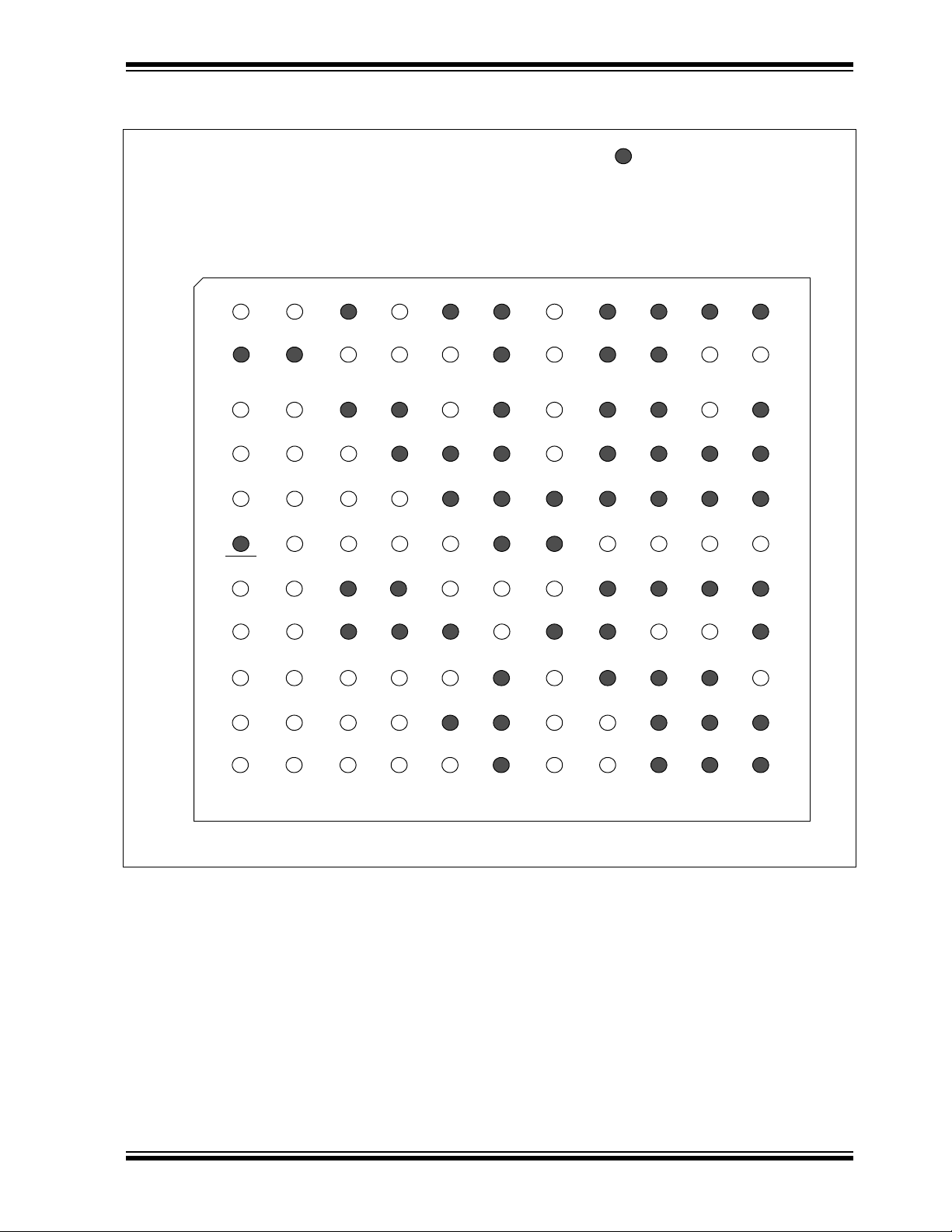
dsPIC33EPXXX(GP/MC/MU)806/810/814 and PIC24EPXXX(GP/GU)810/814
121-Pin TFBGA
(1)
1234567891011
A
RE4 RE3 RG13 RE0 RG0 RF1 VDD NC RD12 RD2 RD1
B
NC RG15 RE2 RE1 RA7 RF0 VCAP RD5 RD3 VSS RC14
C
RE6 VDD RG12 RG14 RA6 NC RD7 RD4 NC RC13 RD11
D
RC1 RE7 RE5 NC NC NC RD6 RD13 RD0 NC RD10
E
RC4 RC3 RG6 RC2 NC RG1 NC RA15 RD8 RD9 RA14
F
MCLR RG8 RG9 RG7 VSS NC NC VDD RC12 VSS RC15
G
RE8 RE9 RA0 NC VDD VSS VSS NC RA5 RA3 RA4
H
RB5 RB4 NC NC NC VDD NC VBUS VUSB3V3 RG2 RA2
J
RB3 RB2 RB7 AVDD RB11 RA1 RB12 NC NC RF8 RG3
K
RB1 RB0 RA10 RB8 NC RF12 RB14 VDD RD15 RF3 RF2
L
RB6 RA9 AVSS RB9 RB10
RF13
RB13 RB15 RD14 RF4 RF5
dsPIC33EP256MU810
Note 1: Refer to Table 2 for full pin names.
= Pins are up to 5V tolerant
dsPIC33EP512MU810
Pin Diagrams (Continued)
© 2009-2012 Microchip Technology Inc. Preliminary DS70616F-page 11
Page 12

dsPIC33EPXXX(GP/MC/MU)806/810/814 and PIC24EPXXX(GP/GU)810/814
TABLE 2: PIN NAMES: dsPIC33EP256MU810 AND dsPIC33EP512MU810
DEVICES
Pin
Number
A1 AN28/PWM3L/PMD4/RP84/RE4 E8 RPI31/RA15
A2 AN27/PWM2H/PMD3/RPI83/RE3 E9 RTCC/DMLN/RPI72/RD8
A3 RP125/RG13 E10 ASDA1/DPLN/RPI73/RD9
A4 AN24/PWM1L/PMD0/RP80/RE0 E11 RPI30/RA14
A5 RP112/RG0 F1 MCLR
A6 VCMPST2/RP97/RF1 F2 C2IN3-/SDO2/PMA3/RP120/RG8
A7 V
A8 No Connect F4 C1IN1-/SDI2/PMA4/RPI119/RG7
A9 RPI76/RD12 F5 V
A10 DPH/RP66/RD2 F6 No Connect
A11 V
B1 No Connect F8 V
B2 RP127/RG15 F9 OSC1/RPI60/RC12
B3 AN26/PWM2L/PMD2/RP82/RE2 F10 V
B4 AN25/PWM1H/PMD1/RPI81/RE1 F11 OSC2/CLKO/RC15
B5 AN23/RPI23/RA7 G1 AN20/RPI88/RE8
B6 V
B7 V
B8 PMRD/RP69/RD5 G4 No Connect
B9 PMBE/RP67/RD3 G5 V
B10 VSS G6 VSS
B11 PGEC2/SOSCO/C3IN1-/T1CK/RPI62/RC14 G7 VSS
C1 AN30/PWM4L/PMD6/RPI86/RE6 G8 No Connect
C2 V
C3 RPI124/RG12 G10 ASDA2/RPI19/RA3
C4 RP126/RG14 G11 TDI/RPI20/RA4
C5 AN22/RPI22/RA6 H1 AN5/C1IN1+/V
C6 No Connect H2 AN4/C1IN2-/USBOEN/RPI36/RB4
C7 C3IN1+/V
C8 PMWR/RP68/RD4 H4 No Connect
C9 No Connect H5 No Connect
C10 PGED2/SOSCI/C3IN3-/RPI61/RC13 H6 V
C11 PMCS1/RPI75/RD11 H7 No Connect
D1 AN16/PWM5L/RPI49/RC1 H8 V
D2 AN31/PWM4H/PMD7/RP87/RE7 H9 VUSB3V3
D3 AN29/PWM3H/PMD5/RP85/RE5 H10 D+/RG2
D4 No Connect H11 ASCL2/RPI18/RA2
D5 No Connect J1 AN3/C2IN1+/VPIO/RPI35/RB3
D6 No Connect J2 AN2/C2IN2-/VMIO/RPI34/RB2
D7 C3IN2-/RP70/RD6 J3 PGED1/AN7/RCV/RPI39/RB7
D8 RPI77/RD13 J4 AV
D9 INT0/DMH/RP64/RD0 J5 AN11/PMA12/RPI43/RB11
D10 No Connect J6 TCK/RPI17/RA1
D11 ASCL1/PMCS2/RPI74/RD10 J7 AN12/PMA11/RPI44/RB12
E1 AN19/PWM6H/RPI52/RC4 J8 No Connect
E2 AN18/PWM6L/RPI51/RC3 J9 No Connect
E3 C1IN3-/SCK2/PMA5/RP118/RG6 J10 RP104/RF8
E4 AN17/PWM5H/RPI50/RC2 J11 D-/RG3
E5 No Connect K1 PGEC3/AN1/RPI33/RB1
E6 RP113/RG1 K2 PGED3/AN0/RPI32/RB0
E7 No Connect K3 V
Note 1: The RPn/RPIn pins can be used by any remappable peripheral with some limitation. See Section 11.4 “Peripheral Pin Select” for
DD F3 C2IN1-/PMA2/RPI121/RG9
CPCON/RP65/RD1 F7 No Connect
CMPST1/RP96/RF0 G2 AN21/RPI89/RE9
CAP G3 TMS/RPI16/RA0
DD G9 TDO/RPI21/RA5
CMPST3/RP71/RD7 H3 No Connect
available peripherals and for information on limitations.
2: Every I/O port pin (RAx-RGx) can be used as change notification (CNAx-CNGx). See Section 11.0 “I/O Ports” for more information.
3: The availability of I
bits, ALTI2C1 and ALTI2C2 (FPOR<5:4>). See Section 29.0 “Special Features” for more information.
(1,2)
Full Pin Name
2
C interfaces varies by device. Selection (SDAx/ SCLx or ASDAx/ASCLx) is made using the device Configuration
Pin
Number
Full Pin Name
SS
DD
SS
DD
BUSON/VBUSST/RPI37/RB5
DD
BUS
DD
REF+/RA10
DS70616F-page 12 Preliminary © 2009-2012 Microchip Technology Inc.
Page 13
dsPIC33EPXXX(GP/MC/MU)806/810/814 and PIC24EPXXX(GP/GU)810/814
TABLE 2: PIN NAMES: dsPIC33EP256MU810 AND dsPIC33EP512MU810
DEVICES
Pin
Number
K4 AN8/PMA6/RPI40/RB8 L3 AVSS
K5 No Connect L4 AN9/PMA7//RPI41/RB9
K6 RP108/RF12 L5 AN10/CV
K7 AN14/PMA1/RPI46/RB14 L6 RP109/RF13
K8 V
K9 RP79/RD15 L8 AN15/PMA0/RPI47/RB15
K10 USBID/RP99/RF3 L9 RPI78/RD14
K11 RP98/RF2 L10 SDA2/PMA9/RP100/RF4
L1 PGEC1/AN6/RPI38/RB6 L11 SCL2/PMA8/RP101/RF5
L2 V
Note 1: The RPn/RPIn pins can be used by any remappable peripheral with some limitation. See Section 11.4 “Peripheral Pin Select” for
DD L7 AN13/PMA10/RPI45/RB13
REF-/RA9
available peripherals and for information on limitations.
2: Every I/O port pin (RAx-RGx) can be used as change notification (CNAx-CNGx). See Section 11.0 “I/O Ports” for more information.
3: The availability of I
bits, ALTI2C1 and ALTI2C2 (FPOR<5:4>). See Section 29.0 “Special Features” for more information.
(1,2)
(CONTINUED)
Full Pin Name
2
C interfaces varies by device. Selection (SDAx/ SCLx or ASDAx/ASCLx) is made using the device Configuration
Pin
Number
Full Pin Name
REF/PMA13/RPI42/RB10
© 2009-2012 Microchip Technology Inc. Preliminary DS70616F-page 13
Page 14
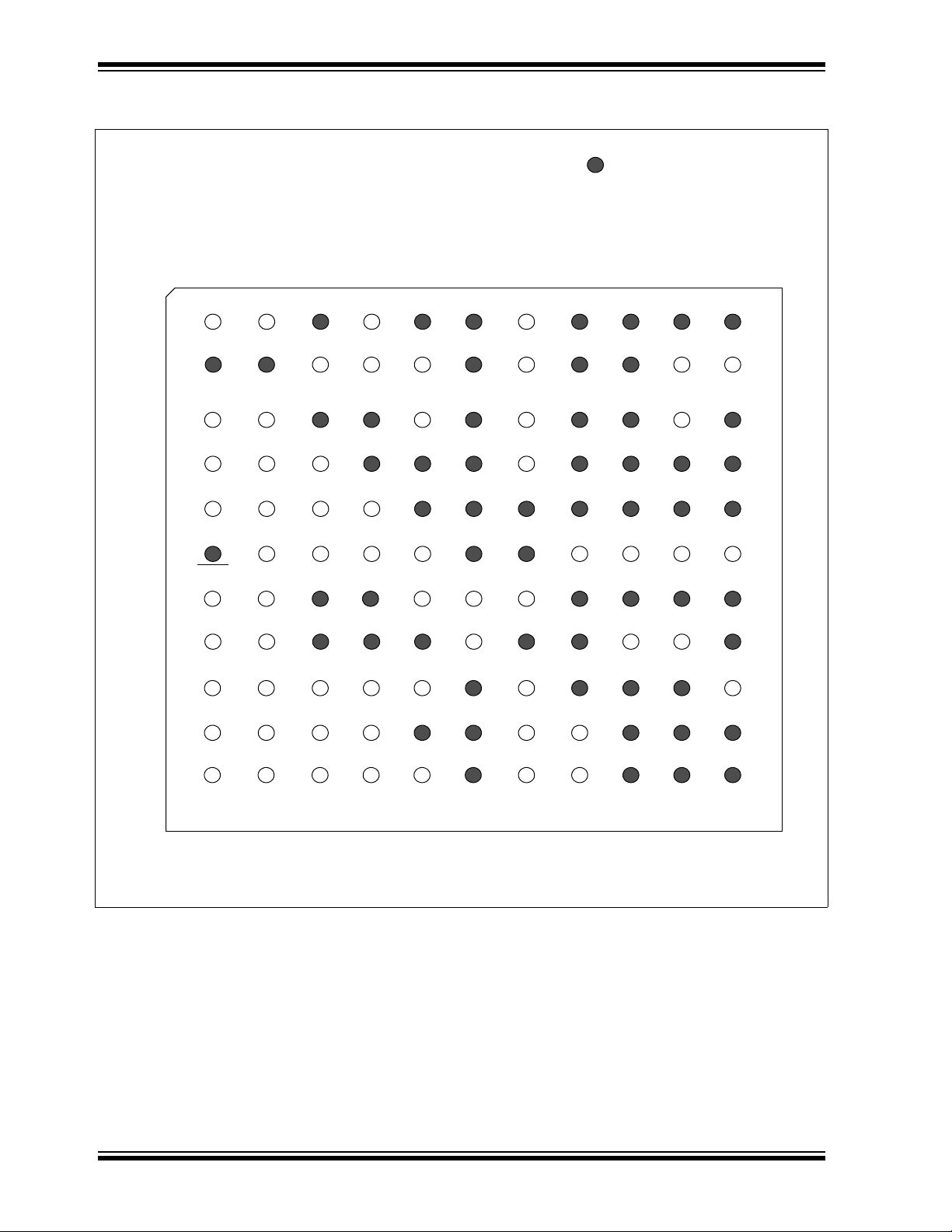
dsPIC33EPXXX(GP/MC/MU)806/810/814 and PIC24EPXXX(GP/GU)810/814
121-Pin TFBGA
(1)
1234567891011
A
RE4 RE3 RG13 RE0 RG0 RF1 VDD NC RD12 RD2 RD1
B
NC RG15 RE2 RE1 RA7 RF0 VCAP RD5 RD3 VSS RC14
C
RE6 VDD RG12 RG14 RA6 NC RD7 RD4 NC RC13 RD11
D
RC1 RE7 RE5 NC NC NC RD6 RD13 RD0 NC RD10
E
RC4 RC3 RG6 RC2 NC RG1 NC RA15 RD8 RD9 RA14
F
MCLR RG8 RG9 RG7 VSS NC NC VDD RC12 VSS RC15
G
RE8 RE9 RA0 NC VDD VSS VSS NC RA5 RA3 RA4
H
RB5 RB4 NC NC NC VDD NC VBUS VUSB3V3 RG2 RA2
J
RB3 RB2 RB7 AVDD RB11 RA1 RB12 NC NC RF8 RG3
K
RB1 RB0 RA10 RB8 NC RF12 RB14 VDD RD15 RF3 RF2
L
RB6 RA9 AVSS RB9 RB10
RF13
RB13 RB15 RD14 RF4 RF5
Note 1: Refer to Table 3 for full pin names.
= Pins are up to 5V tolerant
PIC24EP512GU810
PIC24EP256GU810
Pin Diagrams (Continued)
DS70616F-page 14 Preliminary © 2009-2012 Microchip Technology Inc.
Page 15

dsPIC33EPXXX(GP/MC/MU)806/810/814 and PIC24EPXXX(GP/GU)810/814
TABLE 3: PIN NAMES: PIC24EP256GU810 AND PIC24EP512GU810
DEVICES
Pin
Number
A1 AN28/PMD4/RP84/RE4 E8 RPI31/RA15
A2 AN27/PMD3/RPI83/RE3 E9 RTCC/DMLN/RPI72/RD8
A3 RP125/RG13 E10 ASDA1/DPLN/RPI73/RD9
A4 AN24/PMD0/RP80/RE0 E11 RPI30/RA14
A5 RP112/RG0 F1 MCLR
A6 VCMPST2/RP97/RF1 F2 C2IN3-/SDO2/PMA3/RP120/RG8
A7 V
A8 No Connect F4 C1IN1-/SDI2/PMA4/RPI119/RG7
A9 RPI76/RD12 F5 V
A10 DPH/RP66/RD2 F6 No Connect
A11 V
B1 No Connect F8 V
B2 RP127/RG15 F9 OSC1/RPI60/RC12
B3 AN26/PMD2/RP82/RE2 F10 V
B4 AN25/PMD1/RPI81/RE1 F11 OSC2/CLKO/RC15
B5 AN23/RPI23/RA7 G1 AN20/RPI88/RE8
B6 V
B7 V
B8 PMRD/RP69/RD5 G4 No Connect
B9 PMBE/RP67/RD3 G5 V
B10 VSS G6 VSS
B11 PGEC2/SOSCO/C3IN1-/T1CK/RPI62/RC14 G7 VSS
C1 AN30/PMD6/RPI86/RE6 G8 No Connect
C2 V
C3 RPI124/RG12 G10 ASDA2/RPI19/RA3
C4 RP126/RG14 G11 TDI/RPI20/RA4
C5 AN22/RPI22/RA6 H1 AN5/C1IN1+/V
C6 No Connect H2 AN4/C1IN2-/USBOEN/RPI36/RB4
C7 C3IN1+/V
C8 PMWR/RP68/RD4 H4 No Connect
C9 No Connect H5 No Connect
C10 PGED2/SOSCI/C3IN3-/RPI61/RC13 H6 V
C11 PMCS1/RPI75/RD11 H7 No Connect
D1 AN16/RPI49/RC1 H8 V
D2 AN31/PMD7/RP87/RE7 H9 VUSB3V3
D3 AN29/PMD5/RP85/RE5 H10 D+/RG2
D4 No Connect H11 ASCL2/RPI18/RA2
D5 No Connect J1 AN3/C2IN1+/VPIO/RPI35/RB3
D6 No Connect J2 AN2/C2IN2-/VMIO/RPI34/RB2
D7 C3IN2-/RP70/RD6 J3 PGED1/AN7/RCV/RPI39/RB7
D8 RPI77/RD13 J4 AV
D9 INT0/DMH/RP64/RD0 J5 AN11/PMA12/RPI43/RB11
D10 No Connect J6 TCK/RPI17/RA1
D11 ASCL1/PMCS2/RPI74/RD10 J7 AN12/PMA11/RPI44/RB12
E1 AN19/RPI52/RC4 J8 No Connect
E2 AN18/RPI51/RC3 J9 No Connect
E3 C1IN3-/SCK2/PMA5/RP118/RG6 J10 RP104/RF8
E4 AN17/RPI50/RC2 J11 D-/RG3
E5 No Connect K1 PGEC3/AN1/RPI33/RB1
E6 RP113/RG1 K2 PGED3/AN0/RPI32/RB0
E7 No Connect K3 V
Note 1: The RPn/RPIn pins can be used by any remappable peripheral with some limitation. See Section 11.4 “Peripheral Pin Select” for
DD F3 C2IN1-/PMA2/RPI121/RG9
CPCON/RP65/RD1 F7 No Connect
CMPST1/RP96/RF0 G2 AN21/RPI89/RE9
CAP G3 TMS/RPI16/RA0
DD G9 TDO/RPI21/RA5
CMPST3/RP71/RD7 H3 No Connect
available peripherals and for information on limitations.
2: Every I/O port pin (RAx-RGx) can be used as change notification (CNAx-CNGx). See Section 11.0 “I/O Ports” for more information.
3: The availability of I
bits, ALTI2C1 and ALTI2C2 (FPOR<5:4>). See Section 29.0 “Special Features” for more information.
(1,2)
Full Pin Name
2
C interfaces varies by device. Selection (SDAx/ SCLx or ASDAx/ASCLx) is made using the device Configuration
Pin
Number
Full Pin Name
SS
DD
SS
DD
BUSON/VBUSST/RPI37/RB5
DD
BUS
DD
REF+/RA10
© 2009-2012 Microchip Technology Inc. Preliminary DS70616F-page 15
Page 16
dsPIC33EPXXX(GP/MC/MU)806/810/814 and PIC24EPXXX(GP/GU)810/814
TABLE 3: PIN NAMES: PIC24EP256GU810 AND PIC24EP512GU810
DEVICES
Pin
Number
K4 AN8/PMA6/RPI40/RB8 L3 AVSS
K5 No Connect L4 AN9/PMA7/RPI41/RB9
K6 RP108/RF12 L5 AN10/CV
K7 AN14/PMA1/RPI46/RB14 L6 RP109/RF13
K8 V
K9 RP79/RD15 L8 AN15/PMA0/RPI47/RB15
K10 USBID/RP99/RF3 L9 RPI78/RD14
K11 RP98/RF2 L10 SDA2/PMA9/RP100/RF4
L1 PGEC1/AN6/RPI38/RB6 L11 SCL2/PMA8/RP101/RF5
L2 V
Note 1: The RPn/RPIn pins can be used by any remappable peripheral with some limitation. See Section 11.4 “Peripheral Pin Select” for
DD L7 AN13/PMA10/RPI45/RB13
REF-/RA9
available peripherals and for information on limitations.
2: Every I/O port pin (RAx-RGx) can be used as change notification (CNAx-CNGx). See Section 11.0 “I/O Ports” for more information.
3: The availability of I
bits, ALTI2C1 and ALTI2C2 (FPOR<5:4>). See Section 29.0 “Special Features” for more information.
(1,2)
(CONTINUED)
Full Pin Name
2
C interfaces varies by device. Selection (SDAx/ SCLx or ASDAx/ASCLx) is made using the device Configuration
Pin
Number
Full Pin Name
REF/PMA13/RPI42/RB10
DS70616F-page 16 Preliminary © 2009-2012 Microchip Technology Inc.
Page 17
dsPIC33EPXXX(GP/MC/MU)806/810/814 and PIC24EPXXX(GP/GU)810/814
144-Pin TQFP, 144-pin LQFP
Note 1: The RPn/RPIn pins can be used by any remappable peripheral with some limitation. See
Section 11.4 “Peripheral Pin Select” for available peripherals and for information on limitations.
2: Every I/O port pin (RAx-RKx) can be used as change notification (CNAx-CNKx). See Section 11.0
“I/O Ports” for more information.
3: The availability of I
2
C interfaces varies by device. Selection (SDAx/ SCLx or ASDAx/ASCLx) is made
using the device Configuration bits, ALTI2C1 and ALTI2C2 (FPOR<5:4>). See Section 29.0
“Special Features” for more information.
= Pins are up to 5V tolerant
108
139
1
37
dsPIC33EP512MU814
2
3
4
5
6
7
8
9
10
11
12
13
14
15
16
17
18
19
20
21
22
23
24
25
3839404142434445464748495051525354555657585960
61
107
106
105
104
103
102
101
100
99
98
97
96
95
94
93
92
91
90
89
88
87
86
85
84
138
137
136
135
134
133
132
131
130
129
128
127
126
125
124
123
122
121
120
119
118
117
116
115
144
143
142
141
140
26
27
28
29
30
31
32
33
34
35
36
114
113
112
111
110
109
83
82
81
80
79
78
77
76
75
74
73
6263646566676869707172
AN29/PWM3H/RP85/RE5
AN31/PWM4H/RP87/RE7
C1IN3-/SCK2/RP118/RG6
C1IN1-/SDI2/RPI119/RG7
C2IN3-/SDO2/RP120/RG8
MCLR
C2IN1-/RPI121/RG9
V
DD
AN5/C1IN1+/V
BUSON/VBUSST
/RPI37/RB5
AN4/C1IN2-/USBOEN/RPI36/RB4
AN3/C2IN1+/VPIO/RPI35/RB3
AN2/C2IN2-/VMIO/RPI34/RB2
PGEC3/AN1/RPI33/RB1
PGED3/AN0/RPI32/RB0
V
SS
AN30/PWM4L/RPI86/RE6
V
DD
V
SS
TMS/RPI16/RA0
AN20/RPI88/RE8
AN21/RPI89/RE9
RK0
RK1
RJ14
RJ15
RP127/RG15
PWM7L/PMA8/RJ8
PWM7H/PMA9/RJ9
PMA10/RJ10
PMA11/RJ11
AN16/PWM5L/RPI49/RC1
AN17/PWM5H/RPI50/ RC2
AN18/PWM6L/RPI51/RC3
AN19/PWM6H/RPI52/ RC4
PMA12/RJ12
PMA13/RJ13
AN28/PWM3L/RP84/RE4
AN27/PWM2H/RPI83/RE3
AN26/PWM2L/RP82/RE2
VSSRP125/RG13
RPI124/RG12
RP126/RG14
AN25/PWM1H/RPI81/RE1
AN24/PWM1L/RP80/RE0
PMA7/RJ7
PMA6/RJ6
PMA5/RJ5
PMA4/RJ4
AN23/RPI23/RA7
AN22/RPI22/RA6
RP112/RG0
RP113/RG1
V
CMPST
2/RP97/RF1
V
CMPST
1/RP96/RF0
V
SSVDDVCAP
C3IN1+/V
CMPST
3/RP71/RD7
C3IN2-/RP70/RD6
RP69/RD5
RP68/RD4
PMA3/RJ3
PMA2/RJ2
PMA1/RJ1
PMA0/RJ0
RPI77/RD13
RPI76/RD12
V
DD
RP67/RD3
DPH/RP66/RD2
V
CPCON
/RP65/RD1
V
SS
PGEC2/SOSCO/C3IN1-/T1CK/RPI62/RC14
PGED2/SOSCI/C3IN3-/RPI61/RC13
INT0/DMH/RP64/RD0
RH15
RH14
RH13
RH12
RPI75/RD11
ASCL1/RPI74/RD10
ASDA1/DPLN/RPI73/RD9
RTCC/DMLN/RPI72/RD8
RPI31/RA15
RPI30/RA14
PMCS1/RK11
PMCS2/RK12
V
SS
OSC2/CLKO/RC15
OSC1/RPI60/RC12
V
DD
TDO/RPI21/RA5
TDI/RPI20/RA4
ASDA2/RPI19/RA3
ASCL2/RPI18/RA2
RH11
RH10
RH9
RH8
RP104/RF8
RP98/RF2
USBID/RP99/RF3
V
SS
PGEC1/AN6/RPI38/RB6
PGED1/AN7/RCV/RPI39/RB7
V
REF
-/RA9
V
REF
+/RA10
AV
DD
AV
SS
PMD0/RH0
PMD1/RH1
PMD2/RH2
PMD3/RH3
AN8/RPI40/RB8
AN9/RPI41/RB9
AN10/CV
REF
/RPI42/RB10
AN11/RPI43/RB11
V
SS
V
DD
PMRD/RK15
PMWR/RK14
PMBE/RK13
TCK/RPI17/RA1
RP109/RF13
RP108/RF12
AN12/RPI44/RB12
AN13/RPI45/RB13
AN14/RPI46/RB14
AN15/RPI47/RB15
V
SS
V
DD
PMD4/RH4
PMD5/RH5
PMD6/RH6
PMD7/RH7
RPI78/RD14
RP79/RD15
SDA2/RP100/RF4
SCL2/RP101/RF5
D+/RG2
D-/RG3
V
USB3V
3
V
BUS
dsPIC33EP256MU814
Pin Diagrams (Continued)
© 2009-2012 Microchip Technology Inc. Preliminary DS70616F-page 17
Page 18
dsPIC33EPXXX(GP/MC/MU)806/810/814 and PIC24EPXXX(GP/GU)810/814
144-Pin TQFP, 144-pin LQFP
Note 1: The RPn/RPIn pins can be used by any remappable peripheral with some limitation. See Section 11.4
“Peripheral Pin Select” for available peripherals and for information on limitations.
2: Every I/O port pin (RAx-RKx) can be used as change notification (CNAx-CNKx). See Section 11.0 “I/O
Ports” for more information.
3: The availability of I
2
C interfaces varies by device. Selection (SDAx/ SCLx or ASDAx/ASCLx) is made
using the device Configuration bits, ALTI2C1 and ALTI2C2 (FPOR<5:4>). See Section 29.0 “Special
Features” for more information.
= Pins are up to 5V tolerant
108
139
1
37
2
3
4
5
6
7
8
9
10
11
12
13
14
15
16
17
18
19
20
21
22
23
24
25
3839404142434445464748495051525354555657585960
61
107
106
105
104
103
102
101
100
99
98
97
96
95
94
93
92
91
90
89
88
87
86
85
84
138
137
136
135
134
133
132
131
130
129
128
127
126
125
124
123
122
121
120
119
118
117
116
115
144
143
142
141
140
26
27
28
29
30
31
32
33
34
35
36
114
113
112
111
110
109
83
82
81
80
79
78
77
76
75
74
73
6263646566676869707172
AN29/RP85/RE5
AN31/RP87/RE7
C1IN3-/SCK2/RP118/RG6
C1IN1-/SDI2/RPI119/RG7
C2IN3-/SDO2/RP120/RG8
MCLR
C2IN1-/RPI121/RG9
V
DD
AN5/C1IN1+/V
BUSON/VBUSST
/RPI37/RB5
AN4/C1IN2-/USBOEN/RPI36/RB4
AN3/C2IN1+/VPIO/RPI35/RB3
AN2/C2IN2-/VMIO/RPI34/RB2
PGEC3/AN1/RPI33/RB1
PGED3/AN0/RPI32/RB0
V
SS
AN30/RPI86/RE6
V
DD
V
SS
TMS/RPI16/RA0
AN20/RPI88/RE8
AN21/RPI89/RE9
RK0
RK1
RJ14
RJ15
RP127/RG15
PMA8/RJ8
PMA9/RJ9
PMA10/RJ10
PMA11/RJ11
AN16/RPI49/RC1
AN17/RPI50/RC2
AN18/RPI51/RC3
AN19/RPI52/RC4
PMA12/RJ12
PMA13/RJ13
AN28/RP84/RE4
AN27/RPI83/RE3
AN26/RP82/RE2
VSSRP125/RG13
RPI124/RG12
RP126/RG14
AN25/RPI81/RE1
AN24/RP80/RE0
PMA7/RJ7
PMA6/RJ6
PMA5/RJ5
PMA4/RJ4
AN23/RPI23/RA7
AN22/RPI22/RA6
RP112/RG0
RP113/RG1
V
CMPST
2/RP97/RF1
V
CMPST
1/RP96/RF0
V
SSVDDVCAP
C3IN1+/V
CMPST
3/RP71/RD7
C3IN2-/RP70/RD6
RP69/RD5
RP68/RD4
PMA3/RJ3
PMA2/RJ2
PMA1/RJ1
PMA0/RJ0
RPI77/RD13
RPI76/RD12
V
DD
RP67/RD3
DPH/RP66/RD2
V
CPCON
/RP65/RD1
V
SS
PGEC2/SOSCO/C3IN1-/T1CK/RPI62/RC14
PGED2/SOSCI/C3IN3-/RPI61/RC13
INT0/DMH/RP64/RD0
RH15
RH14
RH13
RH12
RPI75/RD11
ASCL1/RPI74/RD10
ASDA1/DPLN/RPI73/RD9
RTCC/DMLN/RPI72/RD8
RPI31/RA15
RPI30/RA14
PMCS1/RK11
PMCS2/RK12
V
SS
OSC2/CLKO/RC15
OSC1/RPI60/RC12
V
DD
TDO/RPI21/RA5
TDI/RPI20/RA4
ASDA2/RPI19/RA3
ASCL2/RPI18/RA2
RH11
RH10
RH9
RH8
RP104/RF8
RP98/RF2
USBID/RP99/RF3
V
SS
PGEC1/AN6/RPI38/RB6
PGED1/AN7/RCV/RPI39/RB7
V
REF
-/RA9
V
REF
+/RA10
AV
DD
AV
SS
PMD0/RH0
PMD1/RH1
PMD2/RH2
PMD3/RH3
AN8/RPI40/RB8
AN9/RPI41/RB9
AN10/CV
REF
/RPI42/RB10
AN 11/R PI 43/ RB11
V
SS
V
DD
PMRD/RK15
PMWR/RK14
PMBE/RK13
TCK/RPI17/RA1
RP109/RF13
RP108/RF12
AN12/RPI44/RB12
AN13/RPI45/RB13
AN14/RPI46/RB14
AN15/RPI47/RB15
V
SS
V
DD
PMD4/RH4
PMD5/RH5
PMD6/RH6
PMD7/RH7
RPI78/RD14
RP79/RD15
SDA2/RP100/RF4
SCL2/RP101/ RF5
D+/RG2
D-/RG3
V
USB3V
3
V
BUS
PIC24EP512GU814
PIC24EP256GU814
Pin Diagrams (Continued)
DS70616F-page 18 Preliminary © 2009-2012 Microchip Technology Inc.
Page 19

dsPIC33EPXXX(GP/MC/MU)806/810/814 and PIC24EPXXX(GP/GU)810/814
Table of Contents
1.0 Device Overview ........................................................................................................................................................................ 23
2.0 Guidelines for Getting Started with 16-bit Digital Signal Controllers and Microcontrollers ......................................................... 31
3.0 CPU............................................................................................................................................................................................ 37
4.0 Memory Organization ................................................................................................................................................................. 47
5.0 Flash Program Memory............................................................................................................................................................ 135
6.0 Resets ..................................................................................................................................................................................... 141
7.0 Interrupt Controller ................................................................................................................................................................... 145
8.0 Direct Memory Access (DMA) .................................................................................................................................................. 159
9.0 Oscillator Configuration ............................................................................................................................................................ 177
10.0 Power-Saving Features............................................................................................................................................................ 191
11.0 I/O Ports ................................................................................................................................................................................... 205
12.0 Timer1 ...................................................................................................................................................................................... 269
13.0 Timer2/3, Timer4/5, Timer6/7 and Timer8/9 ............................................................................................................................ 273
14.0 Input Capture............................................................................................................................................................................ 279
15.0 Output Compare....................................................................................................................................................................... 285
16.0 High-Speed PWM Module (dsPIC33EPXXX(MC/MU)8XX Devices Only) ............................................................................... 291
17.0 Quadrature Encoder Interface (QEI) Module (dsPIC33EPXXX(MC/MU)8XX Devices Only)................................................... 319
18.0 Serial Peripheral Interface (SPI)............................................................................................................................................... 335
19.0 Inter-Integrated Circuit™ (I
20.0 Universal Asynchronous Receiver Transmitter (UART) ........................................................................................................... 351
21.0 Enhanced CAN (ECAN™) Module........................................................................................................................................... 357
22.0 USB On-The-Go (OTG) Module (dsPIC33EPXXXMU8XX and PIC24EPGU8XX Devices Only) ............................................ 383
23.0 10-bit/12-bit Analog-to-Digital Converter (ADC) ....................................................................................................................... 411
24.0 Data Converter Interface (DCI) Module.................................................................................................................................... 427
25.0 Comparator Module.................................................................................................................................................................. 435
26.0 Real-Time Clock and Calendar (RTCC) .................................................................................................................................. 447
27.0 Programmable Cyclic Redundancy Check (CRC) Generator .................................................................................................. 457
28.0 Parallel Master Port (PMP)....................................................................................................................................................... 463
29.0 Special Features ...................................................................................................................................................................... 473
30.0 Instruction Set Summary .......................................................................................................................................................... 481
31.0 Development Support............................................................................................................................................................... 491
32.0 Electrical Characteristics .......................................................................................................................................................... 495
33.0 DC and AC Device Characteristics Graphs.............................................................................................................................. 569
34.0 Packaging Information.............................................................................................................................................................. 573
Appendix A: Revision History............................................................................................................................................................. 593
2
C™).............................................................................................................................................. 343
© 2009-2012 Microchip Technology Inc. Preliminary DS70616F-page 19
Page 20

dsPIC33EPXXX(GP/MC/MU)806/810/814 and PIC24EPXXX(GP/GU)810/814
TO OUR VALUED CUSTOMERS
It is our intention to provide our valued customers with the best documentation possible to ensure successful use of your Microchip
products. To this end, we will continue to improve our publications to better suit your needs. Our publications will be refined and
enhanced as new volumes and updates are introduced.
If you have any questions or comments regarding this publication, please contact the Marketing Communications Department via
E-mail at docerrors@microchip.com or fax the Reader Response Form in the back of this data sheet to (480) 792-4150. We
welcome your feedback.
Most Current Data Sheet
To obtain the most up-to-date version of this data sheet, please register at our Worldwide Web site at:
http://www.microchip.com
You can determine the version of a data sheet by examining its literature number found on the bottom outside corner of any page.
The last character of the literature number is the version number, (e.g., DS30000A is version A of document DS30000).
Errata
An errata sheet, describing minor operational differences from the data sheet and recommended workarounds, may exist for current
devices. As device/documentation issues become known to us, we will publish an errata sheet. The errata will specify the revision of
silicon and revision of document to which it applies.
To determine if an errata sheet exists for a particular device, please check with one of the following:
• Microchip’s Worldwide Web site; http://www.microchip.com
• Your local Microchip sales office (see last page)
When contacting a sales office, please specify which device, revision of silicon and data sheet (include literature number) you are
using.
Customer Notification System
Register on our web site at www.microchip.com to receive the most current information on all of our products.
DS70616F-page 20 Preliminary © 2009-2012 Microchip Technology Inc.
Page 21

dsPIC33EPXXX(GP/MC/MU)806/810/814 and PIC24EPXXX(GP/GU)810/814
Referenced Sources
This device data sheet is based on the following
individual chapters of the “dsPIC33E/PIC24E Family
Reference Manual”. These documents should be
considered as the general reference for the operation
of a particular module or device feature.
Note: To access the documents listed below,
browse to the documentation section of
the dsPIC33EP512MU814 product page
on the Microchip web site
(www.microchip.com).
In the event you are not able to access
the product page using the link above,
enter this URL in your browser:
http://www.microchip.com/wwwproducts/
Devices.aspx?dDocName=en554310#1
• Section 1. “Introduction” (DS70573)
• Section 2. “CPU” (DS70359)
• Section 3. “Data Memory” (DS70595)
• Section 4. “Program Memory” (DS70613)
• Section 5. “Flash Programming” (DS70609)
• Section 6. “Interrupts” (DS70600)
• Section 7. “Oscillator” (DS70580)
• Section 8. “Reset” (DS70602)
• Section 9. “Watchdog Timer and Power-Saving Modes” (DS70615)
• Section 10. “I/O Ports” (DS70598)
• Section 11. “Timers” (DS70362)
• Section 12. “Input Capture” (DS70352)
• Section 13. “Output Compare” (DS70358)
• Section 14. “High-Speed PWM” (DS70645)
• Section 15. “Quadrature Encoder Interface (QEI)” (DS70601)
• Section 16. “Analog-to-Digital Converter (ADC)” (DS70621)
• Section 17. “UART” (DS70582)
• Section 18. “Serial Peripheral Interface (SPI)” (DS70569)
• Section 19. “Inter-Integrated Circuit™ (I
• Section 20. “Data Converter Interface (DCI)” (DS70356)
• Section 21. “Enhanced Controller Area Network (ECAN™)” (DS70353)
• Section 22. “Direct Memory Access (DMA)” (DS70348)
• Section 23. “CodeGuard™ Security” (DS70634)
• Section 24. “Programming and Diagnostics” (DS70608)
• Section 25. “USB On-The-Go (OTG)” (DS70571)
• Section 26. “Op amp/Comparator” (DS70357)
• Section 27. “Programmable Cyclic Redundancy Check (CRC)” (DS70346)
• Section 28. “Parallel Master Port (PMP)” (DS70576)
• Section 29. “Real-Time Clock and Calendar (RTCC)” (DS70584)
• Section 30. “Device Configuration” (DS70618)
2
C™)” (DS70330)
© 2009-2012 Microchip Technology Inc. Preliminary DS70616F-page 21
Page 22

dsPIC33EPXXX(GP/MC/MU)806/810/814 and PIC24EPXXX(GP/GU)810/814
NOTES:
DS70616F-page 22 Preliminary © 2009-2012 Microchip Technology Inc.
Page 23

dsPIC33EPXXX(GP/MC/MU)806/810/814 and PIC24EPXXX(GP/GU)810/814
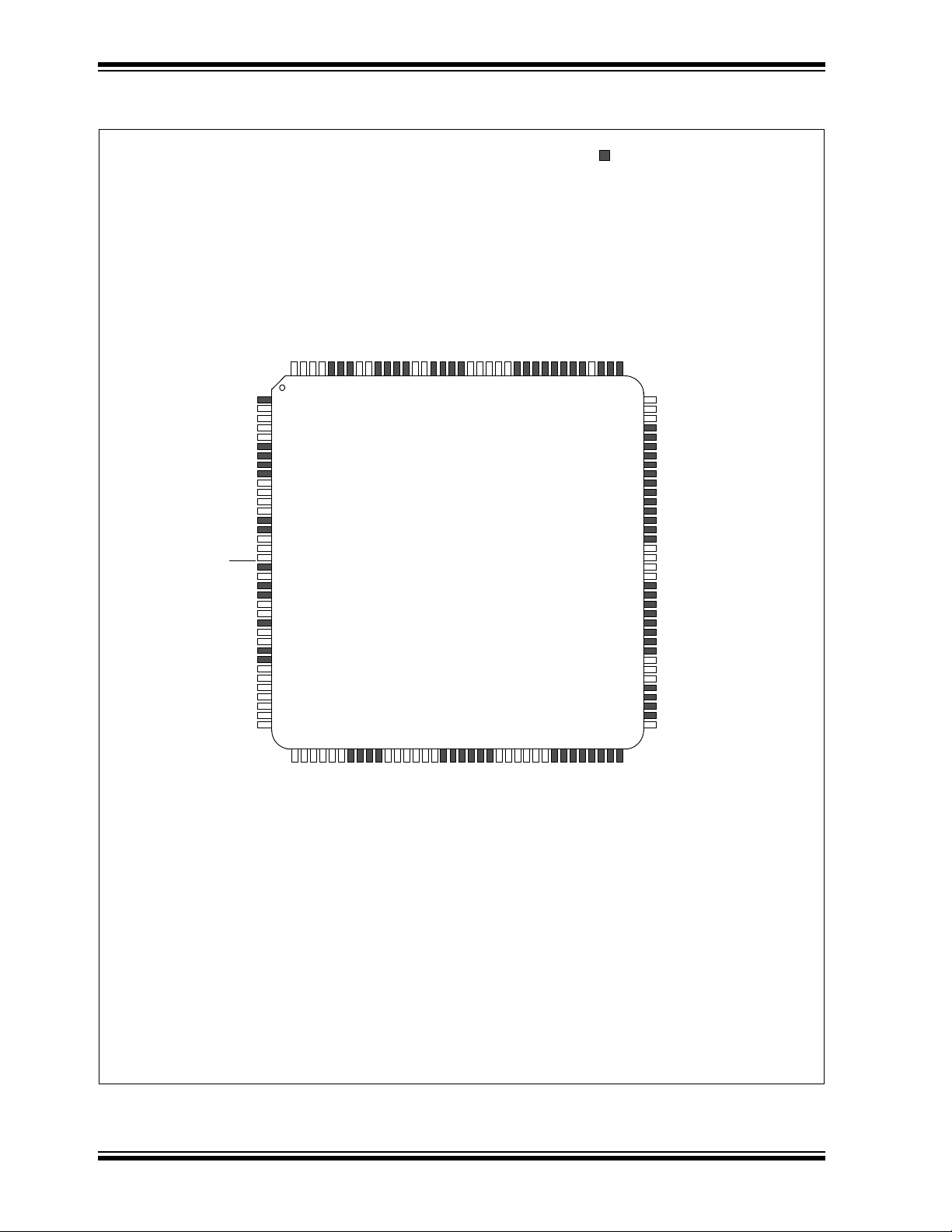
1.0 DEVICE OVERVIEW
Note 1: This data sheet summarizes the features
of the dsPIC33EPXXX(GP/MC/MU)806/
810/814 and PIC24EPXXX(GP/GU)810/
814 families of devices. It is not intended
to be a comprehensive resource. To complement the information in this data
sheet, refer to the related section of the
“dsPIC33E/PIC24E Family Reference
Manual”, which is available from the
Microchip web site (www.microchip.com)
2: Some registers and associated bits
described in this section may not be
available on all devices. Refer to
Section 4.0 “Memory Organization” in
this data sheet for device-specific register
and bit information.
This document contains device-specific information for
the dsPIC33EPXXX(GP/MC/MU)806/810/814 and
PIC24EPXXX(GP/GU)810/814 Digital Signal Controller (DSC) and Microcontroller (MCU) devices. The
dsPIC33EPXXX(GP/MC/MU)806/810/814 devices
contain extensive Digital Signal Processor (DSP) functionality with a high-performance 16-bit MCU
architecture.
Figure 1-1 illustrates a general block diagram of the
core and peripheral modules in the
dsPIC33EPXXX(GP/MC/MU)806/810/814 and
PIC24EPXXX(GP/GU)810/814 families of devices.
Table 1-1 lists the functions of the various pins shown
in the pinout diagrams.
© 2009-2012 Microchip Technology Inc. Preliminary DS70616F-page 23
Page 24
dsPIC33EPXXX(GP/MC/MU)806/810/814 and PIC24EPXXX(GP/GU)810/814
PORTA
PORTB
PORTD
PORTC
Power-up
Timer
Oscillator
Start-up Timer
Instruction
Decode and
Control
OSC1/CLKI
MCLR
VDD, VSS
UART1-
Timing
Generation
ECAN1,
16
PCH PCL
16
Program Counter
16-bit ALU
24
24
24
24
X Data Bus
IR
I2C1,
DCI
PCU
ADC1,
Timers
Input
Capture
Output
Compare
16
16
16
16 x 16
W Reg Array
Divide
Support
Engine
(1)
DSP
ROM Latch
16
Y Data Bus
(1)
EA MUX
X RAGU
X WAGU
Y AGU
(1)
AVDD, AVSS
UART4
SPI4
16
24
16
16
16
16
16
16
16
8
Interrupt
Controller
PSV and Table
Data Access
Control Block
Stac k
Control
Logic
Loop
Control
Logic
Data LatchData Latch
Y Data
RAM
(1)
X Data
RAM
Address
Latch
Address
Latch
Control Signals
to Various Blocks
16
SPI1-
Data Latch
16
16
16
X Address Bus
Y Address Bus
24
Literal Data
ADC2
Program Memory
Watchdog
Timer
POR/BOR
Address Latch
PMP
Comparator
CRC
RTCC
USB
I2C2
ECAN2
QEI1
(1)
,
PWM
(1)
QEI2
(1)
(3 Channel)
PORTE
PORTF
PORTG
PORTH
PORTJ
PORTK
Remappable
Pins
Note 1: This feature or peripheral is only available on dsPIC33EPXXX(MC/MU)806/810/814 devices.
2: This feature or peripheral is only available on dsPIC33EPXXXMU806/810/814 and PIC24EPXXXGU806/810/814 devices.
OTG
(2)
FIGURE 1-1: dsPIC33EPXXX(GP/MC/MU)806/810/814 and PIC24EPXXX(GP/GU)810/814
BLOCK DIAGRAM
DS70616F-page 24 Preliminary © 2009-2012 Microchip Technology Inc.
Page 25
dsPIC33EPXXX(GP/MC/MU)806/810/814 and PIC24EPXXX(GP/GU)810/814
TABLE 1-1: PINOUT I/O DESCRIPTIONS
Pin
Pin Name
AN0-AN31 I Analog No Analog input channels.
CLKI
CLKO
OSC1
OSC2
SOSCI
SOSCO
IC1-IC16 I ST Yes Capture inputs 1 through 16.
OCFA
OCFB
OCFC
OC1-OC16
INT0
INT1
INT2
INT3
INT4
RA0-RA7, RA9,
RA10, RA14, RA15
RB0-RB15 I/O ST No PORTB is a bidirectional I/O port.
RC1-RC4,
RC12-RC15
RD0-RD15 I/O ST No PORTD is a bidirectional I/O port.
RE0-RE9 I/O ST No PORTE is a bidirectional I/O port.
RF0-RF6, RF8
RF12, RF13
RG0, RG1
RG2, RG3
(3)
RG6-RG9,
RG12-RG15
RH0-RH15 I/O ST No PORTH is a bidirectional I/O port.
RJ0-RJ15 I/O ST No PORTJ is a bidirectional I/O port.
Legend: CMOS = CMOS compatible input or output Analog = Analog input P = Power
ST = Schmitt Trigger input with CMOS levels O = Output I = Input
PPS = Peripheral Pin Select TTL = TTL input buffer
Note 1: This pin is available on dsPIC33EPXXX(MC/MU)806/810/814 devices only.
DD must be connected at all times.
2: AV
3: These pins are input only on dsPIC33EPXXXMU8XX and PIC24EPXXXGU8XX devices.
4: These pins are only available on dsPIC33EPXXXMU8XX and PIC24EPXXXGU8XX devices.
5: The availability of I
Selection (SDAx/ SCLx or ASDAx/ASCLx) is made using the device Configuration bits ALTI2C1 and
ALTI2C2 (FPOR<5:4>). See Section 29.0 “Special Features” for more information.
6: Analog functionality is activated by enabling the USB module and is not controlled by the ANSEL register.
Typ e
I
Buffer
Type
CMOS
PPS Description
ST/
NoNoExternal clock source input. Always associated with OSC1 pin function.
Oscillator crystal output. Connects to crystal or resonator in Crystal
Oscillator mode. Optionally functions as CLKO in RC and EC modes.
O
I/O
—
I
ST/
CMOS
—
Always associated with OSC2 pin function.
NoNoOscillator crystal input. ST buffer when configured in RC mode; CMOS
otherwise.
Oscillator crystal output. Connects to crystal or resonator in Crystal
Oscillator mode. Optionally functions as CLKO in RC and EC modes.
I
ST/
NoNo32.768 kHz low-power oscillator crystal input; CMOS otherwise.
CMOS
O
O
—
I
ST
I
ST
I
ST
—
I
ST
I
ST
I
ST
I
ST
I
ST
32.768 kHz low-power oscillator crystal output.
Yes
Compare Fault A input (for Compare channels).
Yes
Compare Fault B input (for Compare channels).
Yes
Compare Fault C input (for Compare channels).
Yes
Compare outputs 1 through 16.
No
External interrupt 0.
Yes
External interrupt 1.
Yes
External interrupt 2.
Yes
External interrupt 3.
Yes
External interrupt 4.
I/O ST No PORTA is a bidirectional I/O port.
I/O ST No PORTC is a bidirectional I/O port.
I/O ST No PORTF is a bidirectional I/O port.
I/O
I/O
I/O
ST
ST
ST
2
C interfaces varies by device. Refer to the “Pin Diagrams” section for availability.
No
PORTG is a bidirectional I/O port.
No
PORTG is a bidirectional I/O port.
No
PORTG is a bidirectional I/O port.
© 2009-2012 Microchip Technology Inc. Preliminary DS70616F-page 25
Page 26
dsPIC33EPXXX(GP/MC/MU)806/810/814 and PIC24EPXXX(GP/GU)810/814
TABLE 1-1: PINOUT I/O DESCRIPTIONS (CONTINUED)
Pin
Pin Name
RK0-RK1,
RK11-RK15
T1CK
T2CK
T3CK
T4CK
T5CK
T6CK
T7CK
T8CK
T9CK
U1CTS
U1RTS
U1RX
U1TX
U2CTS
U2RTS
U2RX
U2TX
U3CTS
U3RTS
U3RX
U3TX
U4CTS
U4RTS
U4RX
U4TX
SCK1
SDI1
SDO1
SS1
SCK2
SDI2
SDO2
SS2
SCK3
SDI3
SDO3
SS3
Legend: CMOS = CMOS compatible input or output Analog = Analog input P = Power
ST = Schmitt Trigger input with CMOS levels O = Output I = Input
PPS = Peripheral Pin Select TTL = TTL input buffer
Note 1: This pin is available on dsPIC33EPXXX(MC/MU)806/810/814 devices only.
DD must be connected at all times.
2: AV
3: These pins are input only on dsPIC33EPXXXMU8XX and PIC24EPXXXGU8XX devices.
4: These pins are only available on dsPIC33EPXXXMU8XX and PIC24EPXXXGU8XX devices.
5: The availability of I
Selection (SDAx/ SCLx or ASDAx/ASCLx) is made using the device Configuration bits ALTI2C1 and
ALTI2C2 (FPOR<5:4>). See Section 29.0 “Special Features” for more information.
6: Analog functionality is activated by enabling the USB module and is not controlled by the ANSEL register.
Typ e
Buffer
Type
PPS Description
I/O ST No PORTK is a bidirectional I/O port.
I
ST
I
ST
I
ST
I
ST
I
ST
I
ST
I
ST
I
ST
I
ST
I
ST
O
I
ST
O
I
ST
O
I
ST
O
I
ST
O
I
ST
O
I
ST
O
I
ST
O
I/O
ST
I
ST
O
I/O
I/O
ST
ST
I
ST
O
I/O
I/O
ST
ST
I
ST
O
I/O
ST
2
C interfaces varies by device. Refer to the “Pin Diagrams” section for availability.
—
—
—
—
—
—
—
—
—
—
—
No
Timer1 external clock input.
Yes
Timer2 external clock input.
Yes
Timer3 external clock input.
Yes
Timer4 external clock input.
Yes
Timer5 external clock input.
Yes
Timer6 external clock input.
Yes
Timer7 external clock input.
Yes
Timer8 external clock input.
Yes
Timer9 external clock input.
Yes
UART1 clear to send.
Yes
UART1 ready to send.
Yes
UART1 receive.
Yes
UART1 transmit.
Yes
UART2 clear to send.
Yes
UART2 ready to send.
Yes
UART2 receive.
Yes
UART2 transmit.
Yes
UART3 clear to send.
Yes
UART3 ready to send.
Yes
UART3 receive.
Yes
UART3 transmit.
Yes
UART4 clear to send.
Yes
UART4 ready to send.
Yes
UART4 receive.
Yes
UART4 transmit.
Yes
Synchronous serial clock input/output for SPI1.
Yes
SPI1 data in.
Yes
SPI1 data out.
Yes
SPI1 slave synchronization or frame pulse I/O.
No
Synchronous serial clock input/output for SPI2.
No
SPI2 data in.
No
SPI2 data out.
Yes
SPI2 slave synchronization or frame pulse I/O.
Yes
Synchronous serial clock input/output for SPI3.
Yes
SPI3 data in.
Yes
SPI3 data out.
Yes
SPI3 slave synchronization or frame pulse I/O.
DS70616F-page 26 Preliminary © 2009-2012 Microchip Technology Inc.
Page 27
dsPIC33EPXXX(GP/MC/MU)806/810/814 and PIC24EPXXX(GP/GU)810/814
TABLE 1-1: PINOUT I/O DESCRIPTIONS (CONTINUED)
Pin
Pin Name
SCK4
SDI4
SDO4
SS4
(5)
SCL1
(5)
SDA1
(5)
ASCL1
(5)
ASDA1
(5)
SCL2
(5)
SDA2
(5)
ASCL2
(5)
ASDA2
TMS
TCK
TDI
TDO
(1)
INDX1
HOME1
QEA1
QEB1
CNTCMP1
INDX2
HOME2
QEA2
QEB2
CNTCMP2
(1)
(1)
(1)
(1)
(1)
(1)
(1)
(1)
(1)
COFS
CSCK
CSDI
CSDO
C1RX
C1TX
C2RX
C2TX
RTCC O — No Real-Time Clock Alarm Output.
REF O Analog No Comparator Voltage Reference Output.
CV
Legend: CMOS = CMOS compatible input or output Analog = Analog input P = Power
ST = Schmitt Trigger input with CMOS levels O = Output I = Input
PPS = Peripheral Pin Select TTL = TTL input buffer
Note 1: This pin is available on dsPIC33EPXXX(MC/MU)806/810/814 devices only.
DD must be connected at all times.
2: AV
3: These pins are input only on dsPIC33EPXXXMU8XX and PIC24EPXXXGU8XX devices.
4: These pins are only available on dsPIC33EPXXXMU8XX and PIC24EPXXXGU8XX devices.
5: The availability of I
Selection (SDAx/ SCLx or ASDAx/ASCLx) is made using the device Configuration bits ALTI2C1 and
ALTI2C2 (FPOR<5:4>). See Section 29.0 “Special Features” for more information.
6: Analog functionality is activated by enabling the USB module and is not controlled by the ANSEL register.
Typ e
I/O
I
O
I/O
I/O
I/O
I/O
I/O
I/O
I/O
I/O
I/O
I
I
I
O
I
I
I
Buffer
Type
PPS Description
ST
Yes
Synchronous serial clock input/output for SPI4.
ST
Yes
SPI4 data in.
—
Yes
SPI4 data out.
ST
Yes
SPI4 slave synchronization or frame pulse I/O.
ST
ST
ST
ST
ST
ST
ST
ST
ST
ST
ST
ST
ST
ST
—
No
Synchronous serial clock input/output for I2C1.
No
Synchronous serial data input/output for I2C1.
No
Alternate synchronous serial clock input/output for I2C1.
No
Alternate synchronous serial data input/output for I2C1.
No
Synchronous serial clock input/output for I2C2.
No
Synchronous serial data input/output for I2C2.
No
Alternate synchronous serial clock input/output for I2C2.
No
Alternate synchronous serial data input/output for I2C2.
No
JTAG Test mode select pin.
No
JTAG test clock input pin.
No
JTAG test data input pin.
No
JTAG test data output pin.
Yes
Quadrature Encoder Index1 Pulse input.
Yes
Quadrature Encoder Home1 Pulse input.
Yes
Quadrature Encoder Phase A input in QEI1 mode. Auxiliary Timer
External Clock input in Timer mode.
I
ST
Yes
Quadrature Encoder Phase A input in QEI1 mode. Auxiliary Timer
External Gate input in Timer mode.
O
—
Yes
Quadrature Encoder Compare Output 1.
I
ST
Yes
Quadrature Encoder Index2 Pulse input.
I
ST
Yes
Quadrature Encoder Home2 Pulse input.
I
ST
Yes
Quadrature Encoder Phase A input in QEI2 mode. Auxiliary Timer
External Clock input in Timer mode.
I
ST
Yes
Quadrature Encoder Phase B input in QEI2 mode. Auxiliary Timer
External Gate input in Timer mode.
O
I/O
I/O
O
O
O
—
Yes
Quadrature Encoder Compare Output 2.
ST
Yes
Data Converter Interface frame synchronization pin.
ST
Yes
Data Converter Interface serial clock input/output pin.
I
ST
Yes
Data Converter Interface serial data input pin.
—
Yes
Data Converter Interface serial data output pin.
I
ST—Yes
I
ST—Yes
2
C interfaces varies by device. Refer to the “Pin Diagrams” section for availability.
ECAN1 bus receive pin.
Yes
ECAN1 bus transmit pin.
ECAN2 bus receive pin.
Yes
ECAN2 bus transmit pin.
© 2009-2012 Microchip Technology Inc. Preliminary DS70616F-page 27
Page 28
dsPIC33EPXXX(GP/MC/MU)806/810/814 and PIC24EPXXX(GP/GU)810/814
TABLE 1-1: PINOUT I/O DESCRIPTIONS (CONTINUED)
Pin
Pin Name
C1IN1+, C1IN2-,
C1IN1-, C1IN3-
C1OUT
C2IN1+, C2IN2-,
C2IN1-, C2IN3C2OUT
C3IN1+, C3IN2-,
C2IN1-, C3IN3C3OUT
PMA0
PMA1
PMA2 -PMA13
PMBE
PMCS1, PMCS2
PMD0-PMD7
PMRD
PMWR
FLT1
DTCMP1-DTCMP7
PWM1L-PWM7L
PWM1H-PWM7H
SYNCI1, SYNCI2
SYNCO1, SYNCO2
(1)
(1)
(1)
(1)
(1)
(1)
-FLT7
Legend: CMOS = CMOS compatible input or output Analog = Analog input P = Power
ST = Schmitt Trigger input with CMOS levels O = Output I = Input
PPS = Peripheral Pin Select TTL = TTL input buffer
Note 1: This pin is available on dsPIC33EPXXX(MC/MU)806/810/814 devices only.
DD must be connected at all times.
2: AV
3: These pins are input only on dsPIC33EPXXXMU8XX and PIC24EPXXXGU8XX devices.
4: These pins are only available on dsPIC33EPXXXMU8XX and PIC24EPXXXGU8XX devices.
5: The availability of I
Selection (SDAx/ SCLx or ASDAx/ASCLx) is made using the device Configuration bits ALTI2C1 and
ALTI2C2 (FPOR<5:4>). See Section 29.0 “Special Features” for more information.
6: Analog functionality is activated by enabling the USB module and is not controlled by the ANSEL register.
Buffer
Typ e
Type
IOAnalog—No
IOAnalog—No
IOAnalog—No
I/O
TTL/ST
PPS Description
Comparator 1 Inputs
Yes
Comparator 1 Output.
Comparator 2 Inputs.
Yes
Comparator 2 Output.
Comparator 3 Inputs.
Yes
Comparator 3 Output.
No
Parallel Master Port Address Bit 0 Input (Buffered Slave modes) and
Output (Master modes).
I/O
TTL/ST
No
Parallel Master Port Address Bit 1 Input (Buffered Slave modes) and
Output (Master modes).
O
O
O
I/O
—
—
—
TTL/ST
No
Parallel Master Port Address Bits 2 - 13 (Demultiplexed Master Modes).
No
Parallel Master Port Byte Enable Strobe.
No
Parallel Master Port Chip Select 1 and 2 Strobe.
No
Parallel Master Port Data (Demultiplexed Master mode) or Address/
Data (Multiplexed Master modes).
O
O
O
O
O
—
No
Parallel Master Port Read Strobe.
—
No
Parallel Master Port Write Strobe.
I
ST
Yes
PWM Fault input 1 through 7.
I
ST
Yes
PWM Dead Time Compensation Input.
—
No
PWM Low output 1 through 7.
—
No
PWM High output 1 through 7.
I
ST
Yes
PWM Synchronization Inputs 1 and 2.
—
Yes
PWM Synchronization Output 1 and 2.
2
C interfaces varies by device. Refer to the “Pin Diagrams” section for availability.
DS70616F-page 28 Preliminary © 2009-2012 Microchip Technology Inc.
Page 29

dsPIC33EPXXX(GP/MC/MU)806/810/814 and PIC24EPXXX(GP/GU)810/814
TABLE 1-1: PINOUT I/O DESCRIPTIONS (CONTINUED)
Pin
Pin Name
(4,6)
VBUS
VUSB
VBUSON
D+
DUSBID
USBOEN
VBUSST
VCPCON
VCMPST1
VCMPST2
VCMPST3
VMIO
VPIO
DMH
DPH
DMLN
DPLN
RCV
(4,6)
(4,6)
3V3
(4)
(4)
(4)
(4)
(4)
(4)
(4)
(4)
(4)
(4)
(4)
(4)
(4)
(4)
(4)
(4)
PGED1
PGEC1
PGED2
PGEC2
PGED3
PGEC3
MCLR
Legend: CMOS = CMOS compatible input or output Analog = Analog input P = Power
ST = Schmitt Trigger input with CMOS levels O = Output I = Input
PPS = Peripheral Pin Select TTL = TTL input buffer
Note 1: This pin is available on dsPIC33EPXXX(MC/MU)806/810/814 devices only.
DD must be connected at all times.
2: AV
3: These pins are input only on dsPIC33EPXXXMU8XX and PIC24EPXXXGU8XX devices.
4: These pins are only available on dsPIC33EPXXXMU8XX and PIC24EPXXXGU8XX devices.
5: The availability of I
Selection (SDAx/ SCLx or ASDAx/ASCLx) is made using the device Configuration bits ALTI2C1 and
ALTI2C2 (FPOR<5:4>). See Section 29.0 “Special Features” for more information.
6: Analog functionality is activated by enabling the USB module and is not controlled by the ANSEL register.
Buffer
Typ e
I
Type
Analog
P
O
I/O
Analog
I/O
Analog
I
O
I
O
I
I
I
I/O
I/O
O
O
O
O
I
I/O
I
I/O
I
I/O
I
I/P ST No
PPS Description
No
USB Bus Power Monitor.
—
No
USB Internal Transceiver Supply. If the USB module is not being used,
this pin must be connected to V
—
ST
—
ST
—
ST
ST
ST
ST
ST
—
—
—
—
ST
ST
ST
ST
ST
ST
ST
USB Host and On-The-Go (OTG) Bus Power Control Output.
No
D+ pin of internal USB Transceiver.
No
D- pin of internal USB Transceiver.
No
USB OTG ID Detect.
No
USB Output Enabled Control (for external transceiver).
No
USB Boost Controller Overcurrent Detection.
No
USB Boost Controller PWM Signal.
No
USB External Comparator 1 Input.
No
USB External Comparator 2 Input.
No
USB External Comparator 3 Input.
No
USB Differential Minus Input/Output (external transceiver).
No
USB Differential Plus Input/Output (external transceiver).
No
D- External Pull-up Control Output.
No
D+ External Pull-up Control Output.
No
D- External Pull-down Control Output.
No
D+ External Pull-down Control Output.
No
USB Receive Input (from external transceiver).
No
No
Data I/O pin for programming/debugging communication channel 1.
No
Clock input pin for programming/debugging communication channel 1.
No
Data I/O pin for programming/debugging communication channel 2.
No
Clock input pin for programming/debugging communication channel 2.
No
Data I/O pin for programming/debugging communication channel 3.
No
Clock input pin for programming/debugging communication channel 3.
Master Clear (Reset) input. This pin is an active-low Reset to the
DD.
device.
2
C interfaces varies by device. Refer to the “Pin Diagrams” section for availability.
© 2009-2012 Microchip Technology Inc. Preliminary DS70616F-page 29
Page 30
dsPIC33EPXXX(GP/MC/MU)806/810/814 and PIC24EPXXX(GP/GU)810/814
TABLE 1-1: PINOUT I/O DESCRIPTIONS (CONTINUED)
Pin
Pin Name
(2)
AVDD
AVSS P P No Ground reference for analog modules.
VDD P — No Positive supply for peripheral logic and I/O pins.
V
CAP P — No CPU logic filter capacitor connection.
V
SS P — No Ground reference for logic and I/O pins.
VREF+ I Analog No Analog voltage reference (high) input.
V
REF- I Analog No Analog voltage reference (low) input.
Legend: CMOS = CMOS compatible input or output Analog = Analog input P = Power
ST = Schmitt Trigger input with CMOS levels O = Output I = Input
PPS = Peripheral Pin Select TTL = TTL input buffer
Note 1: This pin is available on dsPIC33EPXXX(MC/MU)806/810/814 devices only.
DD must be connected at all times.
2: AV
3: These pins are input only on dsPIC33EPXXXMU8XX and PIC24EPXXXGU8XX devices.
4: These pins are only available on dsPIC33EPXXXMU8XX and PIC24EPXXXGU8XX devices.
5: The availability of I
Selection (SDAx/ SCLx or ASDAx/ASCLx) is made using the device Configuration bits ALTI2C1 and
ALTI2C2 (FPOR<5:4>). See Section 29.0 “Special Features” for more information.
6: Analog functionality is activated by enabling the USB module and is not controlled by the ANSEL register.
Typ e
Buffer
Type
PPS Description
P P No Positive supply for analog modules. This pin must be connected at all
times.
2
C interfaces varies by device. Refer to the “Pin Diagrams” section for availability.
DS70616F-page 30 Preliminary © 2009-2012 Microchip Technology Inc.
Page 31

dsPIC33EPXXX(GP/MC/MU)806/810/814 and PIC24EPXXX(GP/GU)810/814
2.0 GUIDELINES FOR GETTING STARTED WITH 16-BIT DIGITAL SIGNAL CONTROLLERS AND MICROCONTROLLERS
Note 1: This data sheet summarizes the features
of the
dsPIC33EPXXX(GP/MC/MU)806/810/81
4 and PIC24EPXXX(GP/GU)810/814
families of devices. It is not intended to be
a comprehensive reference source. To
complement the information in this data
sheet, refer to the related section of the
“dsPIC33E/PIC24E Family Reference
Manual”, which is available from the
Microchip web site (www.microchip.com)
2: Some registers and associated bits
described in this section may not be
available on all devices. Refer to
Section 4.0 “Memory Organization” in
this data sheet for device-specific register
and bit information.
2.1 Basic Connection Requirements
Getting started with the 16-bit DSCs and microcontrollers
requires attention to a minimal set of device pin
connections before proceeding with development. The
following is a list of pin names, which must always be
connected:
DD and VSS pins (see Section 2.2
• All V
“Decoupling Capacitors”)
• All AVDD and AVSS pins (regardless if ADC module
is not used) (see Section 2.2 “Decoupling
Capacitors”)
CAP (see Section 2.3 “CPU Logic Filter
•V
Capacitor Connection (V
•MCLR
• PGECx/PGEDx pins used for In-Circuit Serial
• OSC1 and OSC2 pins when external oscillator
Additionally, the following pins may be required:
•V
•V
pin (see Section 2.4 “Master Clear (MCLR)
Pin”)
Programming™ (ICSP™) and debugging purposes
(see Section 2.5 “ICSP Pins”)
source is used (see Section 2.6 “External
Oscillator Pins”)
USB3V3 pin is used when utilizing the USB
module. If the USB module is not used, V
must be connected to V
REF+/VREF- pin is used when external voltage
reference for ADC module is implemented
Note: The AV
connected independent of the ADC
voltage reference source. The voltage
difference between AV
exceed 300 mV at any time during
operation or start-up.
DD and AVSS pins must be
CAP)”)
USB3V3
DD.
DD and VDD cannot
2.2 Decoupling Capacitors
The use of decoupling capacitors on every pair of
power supply pins, such as V
AVDD and AVSS is required.
Consider the following criteria when using decoupling
capacitors:
• Value and type of capacitor: Recommendation of
0.1 µF (100 nF), 10-20V. This capacitor should be a
low-ESR and have resonance frequency in the
range of 20 MHz and higher. It is recommended to
use ceramic capacitors.
• Placement on the printed circuit board: The
decoupling capacitors should be placed as close to
the pins as possible. It is recommended to place the
capacitors on the same side of the board as the
device. If space is constricted, the capacitor can be
placed on another layer on the PCB using a via;
however, ensure that the trace length from the pin to
the capacitor is within one-quarter inch (6 mm) in
length.
• Handling high frequency noise: If the board is
experiencing high frequency noise, above tens of
MHz, add a second ceramic-type capacitor in parallel to the above described decoupling capacitor. The
value of the second capacitor can be in the range of
0.01 µF to 0.001 µF. Place this second capacitor
next to the primary decoupling capacitor. In
high-speed circuit designs, consider implementing a
decade pair of capacitances as close to the power
and ground pins as possible. For example, 0.1 µF in
parallel with 0.001 µF.
• Maximizing performance: On the board layout
from the power supply circuit, run the power and
return traces to the decoupling capacitors first, and
then to the device pins. This ensures that the decoupling capacitors are first in the power chain. Equally
important is to keep the trace length between the
capacitor and the power pins to a minimum, thereby
reducing PCB track inductance.
DD, VSS, VUSB3V3,
© 2009-2012 Microchip Technology Inc. Preliminary DS70616F-page 31
Page 32

dsPIC33EPXXX(GP/MC/MU)806/810/814 and PIC24EPXXX(GP/GU)810/814
dsPIC33EP/
VDD
VSS
VDD
VSS
VSS
VDD
AVDD
AVSS
VDD
VSS
0.1 µF
Ceramic
0.1 µF
Ceramic
0.1 µF
Ceramic
0.1 µF
Ceramic
C
R
V
DD
MCLR
0.1 µF
Ceramic
VCAP
L1
(2)
R1
10 µF
Tantalum
Note 1: If the USB module is not used, VUSB3V3 must be
connected to V
DD, as shown.
2: As an option, instead of a hard-wired connection, an
inductor (L1) can be substituted between V
DD and
AV
DD to improve ADC noise rejection. The inductor
impedance should be less than 1Ω and the inductor
capacity greater than 10 mA.
Where:
f
FCNV
2
--------------=
f
1
2π LC()
-----------------------=
L
1
2πfC()
---------------------
⎝⎠
⎛⎞
2
=
(i.e., ADC conversion rate/2)
V
USB3V3
(1)
PIC24EP
Note 1: R ≤ 10 kΩ is recommended. A suggested
starting value is 10 kΩ. Ensure that the MCLR
pin VIH and VIL specifications are met.
2: R1 ≤ 470Ω will limit any current flowing into
MCLR from the external capacitor C, in the
event of MCLR
pin breakdown, due to
Electrostatic Discharge (ESD) or Electrical
Overstress (EOS). Ensure that the MCLR
pin
V
IH and VIL specifications are met.
C
R1
(2)
R
(1)
VDD
MCLR
dsPIC33EP
JP
FIGURE 2-1: RECOMMENDED
MINIMUM CONNECTION
to ground. The type can be ceramic or tantalum. See
Section 32.0 “Electrical Characteristics” for
additional information.
The placement of this capacitor should be close to the
CAP. It is recommended that the trace length not
V
exceeds one-quarter inch (6 mm). See Section 29.2
“On-Chip Voltage Regulator” for details.
2.4 Master Clear (MCLR) Pin
The MCLR pin provides two specific device
functions:
• Device Reset
• Device Programming and Debugging
During device programming and debugging, the
resistance and capacitance that can be added to the
pin must be considered. Device programmers and
debuggers drive the MCLR
specific voltage levels (VIH and VIL) and fast signal
transitions must not be adversely affected. Therefore,
specific values of R and C will need to be adjusted
based on the application and PCB requirements.
For example, as shown in Figure 2-2, it is
recommended that the capacitor C, be isolated from
the MCLR
pin during programming and debugging
operations.
Place the components as shown in Figure 2-2 within
one-quarter inch (6 mm) from the MCLR
pin. Consequently,
pin.
2.2.1 TANK CAPACITORS
On boards with power traces running longer than six
inches in length, it is suggested to use a tank capacitor
for integrated circuits including DSCs to supply a local
power source. The value of the tank capacitor should
be determined based on the trace resistance that connects the power supply source to the device, and the
maximum current drawn by the device in the application. In other words, select the tank capacitor so that it
meets the acceptable voltage sag at the device. Typical
values range from 4.7 µF to 47 µF.
2.3 CPU Logic Filter Capacitor
A low-ESR (< 1 Ohms) capacitor is required on the
CAP pin, which is used to stabilize the voltage
V
regulator output voltage. The V
connected to VDD, and must have a capacitor greater
than 4.7 µF (10 µF is recommended), 16V connected
DS70616F-page 32 Preliminary © 2009-2012 Microchip Technology Inc.
Connection (V
CAP)
FIGURE 2-2: EXAMPLE OF MCLR PIN
CONNECTIONS
CAP pin must not be
Page 33

dsPIC33EPXXX(GP/MC/MU)806/810/814 and PIC24EPXXX(GP/GU)810/814
13
Main Oscillator
Guard Ring
Guard Trace
Secondary
Oscillator
14
15
16
17
18
19
20
2.5 ICSP Pins
The PGECx and PGEDx pins are used for ICSP and
debugging purposes. It is recommended to keep the
trace length between the ICSP connector and the ICSP
pins on the device as short as possible. If the ICSP connector is expected to experience an ESD event, a
series resistor is recommended, with the value in the
range of a few tens of Ohms, not to exceed 100 Ohms.
Pull-up resistors, series diodes and capacitors on the
PGECx and PGEDx pins are not recommended as they
will interfere with the programmer/debugger communications to the device. If such discrete components are
an application requirement, they should be removed
from the circuit during programming and debugging.
Alternatively, refer to the AC/DC characteristics and
timing requirements information in the respective
device Flash programming specification for information
on capacitive loading limits and pin input voltage high
IH) and input low (VIL) requirements.
(V
Ensure that the “Communication Channel Select” (i.e.,
PGECx/PGEDx pins) programmed into the device
matches the physical connections for the ICSP to
®
MPLAB
ICE™.
For more information on MPLAB ICD 3 and MPLAB
REAL ICE connection requirements, refer to the
following documents that are available on the
Microchip web site.
• “Using MPLAB
• “MPLAB
• “MPLAB
• “Using MPLAB
PICkit™ 3, MPLAB ICD 3, or MPLAB REAL
®
®
®
ICD 3” (poster) DS51765
ICD 3 Design Advisory” DS51764
REAL ICE™ In-Circuit Emulator User’s
Guide” DS51616
®
REAL ICE™ In-Circuit Emulator”
(poster) DS51749
FIGURE 2-3: SUGGESTED PLACEMENT
OF THE OSCILLATOR
CIRCUIT
2.7 Oscillator Value Conditions on Device Start-up
If the PLL of the target device is enabled and
configured for the device start-up oscillator, the
maximum oscillator source frequency must be limited
to 3 MHz < F
start-up conditions. This means that if the external
oscillator frequency is outside this range, the
application must start-up in the FRC mode first. The
default PLL settings after a POR with an oscillator
frequency outside this range will violate the device
operating speed.
Once the device powers up, the application firmware
can initialize the PLL SFRs, CLKDIV and PLLDBF to a
suitable value, and then perform a clock switch to the
Oscillator + PLL clock source. Note that clock switching
must be enabled in the device Configuration Word.
IN < 5.5 MHz to comply with device PLL
2.6 External Oscillator Pins
Many DSCs have options for at least two oscillators: a
high-frequency primary oscillator and a low-frequency
secondary oscillator. For details, see Section 9.0
“Oscillator Configuration” for details.
2.8 Unused I/Os
Unused I/O pins should be configured as outputs and
driven to a logic-low state.
Alternatively, connect a 1k to 10k resistor between V
and unused pins and drive the output to logic low.
SS
The oscillator circuit should be placed on the same
side of the board as the device. Also, place the
oscillator circuit close to the respective oscillator pins,
not exceeding one-half inch (12 mm) distance
between them. The load capacitors should be placed
next to the oscillator itself, on the same side of the
board. Use a grounded copper pour around the
oscillator circuit to isolate them from surrounding
circuits. The grounded copper pour should be routed
directly to the MCU ground. Do not run any signal
traces or power traces inside the ground pour. Also, if
using a two-sided board, avoid any traces on the
other side of the board where the crystal is placed. A
suggested layout is shown in Figure 2-3.
© 2009-2012 Microchip Technology Inc. Preliminary DS70616F-page 33
Page 34

dsPIC33EPXXX(GP/MC/MU)806/810/814 and PIC24EPXXX(GP/GU)810/814
IPFC
VOUTPUT
ADC Channel ADC Channel
PWM
k
1
k
2
k
3
FET
dsPIC33EP
VINPUT
Comparator
Output
Driver
2.9 Application Examples
• Speech (playback, hands-free kits, answering
machines, VoIP)
• Induction heating
• Uninterruptable Power Supplies (UPS)
• DC/AC inverters
• Compressor motor control
• Washing machine 3-phase motor control
• BLDC motor control
• Automotive HVAC, cooling fans, fuel pumps
• Stepper motor control
• Audio and fluid sensor monitoring
• Consumer audio
• Industrial and building control (security systems
and access control)
• Barcode reading
• Networking: LAN switches, gateways
• Data storage device management
• Smart cards and smart card readers
Examples of typical application connections are shown
in Figure 2-4 through Figure 2-8.
• Camera lens focus and stability control
FIGURE 2-4: BOOST CONVERTER IMPLEMENTATION
DS70616F-page 34 Preliminary © 2009-2012 Microchip Technology Inc.
Page 35
dsPIC33EPXXX(GP/MC/MU)806/810/814 and PIC24EPXXX(GP/GU)810/814
k
1
Comparator
k
2
k
7
PWM
PWM
ADC
Channel
ADC
Channel
5V Output
I
5V
12V Input
FET
Driver
dsPIC33EP
k
5
k
4
k
3
k
6
k
7
Comparator
Comparator
ADC Channel
Comparator
ADC
Channel
PWM
PWM
PWM
PWM
PWM
PWM
3.3V Output
12V Input
FET
Driver
FET
Driver
FET
Driver
dsPIC33EP
FIGURE 2-5: SINGLE-PHASE SYNCHRONOUS BUCK CONVERTER
FIGURE 2-6: MULTI-PHASE SYNCHRONOUS BUCK CONVERTER
© 2009-2012 Microchip Technology Inc. Preliminary DS70616F-page 35
Page 36

dsPIC33EPXXX(GP/MC/MU)806/810/814 and PIC24EPXXX(GP/GU)810/814
VAC
VOUT+
Comparator
PWM
ADC
PWM
|V
AC|
k
4
k
3
FET
dsPIC33EP
Driver
V
OUT-
ADC Channel
FET
Driver
k
1
k
2
Comparator
Channel
Comparator
3-Phase
Inverter
PWM3H
PWM3L
PWM2H
PWM2L
PWM1H
PWM1L
FLTx
Fault
BLDC
dsPIC33EP/PIC24EP
AN3
AN4
AN5
AN2
Demand
Phase Terminal Voltage Feedback
R49 R41 R34
R36
R44
R52
FIGURE 2-7: INTERLEAVED PFC
FIGURE 2-8: BEMF VOLTAGE MEASURED USING THE ADC MODULE
DS70616F-page 36 Preliminary © 2009-2012 Microchip Technology Inc.
Page 37

dsPIC33EPXXX(GP/MC/MU)806/810/814 and PIC24EPXXX(GP/GU)810/814
3.0 CPU
Note 1: This data sheet summarizes the features
of the dsPIC33EPXXX(GP/MC/MU)806/
810/814 and PIC24EPXXX(GP/GU)810/
814 families of devices. It is not intended
to be a comprehensive reference source.
To complement the information in this
data sheet, refer to Section 2. “CPU”
(DS70359) in the “dsPIC33E/PIC24E
Family Reference Manual”, which is
available from the Microchip web site
(www.microchip.com).
2: Some registers and associated bits
described in this section may not be
available on all devices. Refer to
Section 4.0 “Memory Organization” in
this data sheet for device-specific register
and bit information.
The CPU has a 16-bit (data) modified Harvard architecture with an enhanced instruction set, including significant support for digital signal processing. The CPU has
a 24-bit instruction word, with a variable length opcode
field. The Program Counter (PC) is 24 bits wide and
addresses up to 4M x 24 bits of user program memory
space.
An instruction prefetch mechanism helps maintain
throughput and provides predictable execution. Most
instructions execute in a single-cycle effective execution rate, with the exception of instructions that change
the program flow, the double-word move (MOV.D)
instruction, PSV accesses, and the table instructions.
Overhead free program loop constructs are supported
using the DO and REPEAT instructions, both of which
are interruptible at any point.
3.1 Registers
Devices have sixteen 16-bit Working registers in the
programmer’s model. Each of the Working registers
can act as a data, address or address offset register.
The 16th Working register (W15) operates as a software Stack Pointer for interrupts and calls. The working
registers, W0 through W3, and selected bits from the
STATUS register, have shadow registers for fast context saves and restores using a single POP.S or
PUSH.S instruction.
3.2 Instruction Set
The dsPIC33EPXXXMU806/810/814 instruction set
has two classes of instructions: the MCU class of
instructions and the DSP class of instructions. The
PIC24EPXXX(GP/GU)810/814 instruction set has the
MCU class of instructions and does not support DSP
instructions. These two instruction classes are seamlessly integrated into the architecture and execute from
a single execution unit. The instruction set includes
many addressing modes and was designed for optimum C compiler efficiency.
3.3 Data Space Addressing
The base data space can be addressed as 32K words
or 64 Kbytes and is split into two blocks, referred to as
X and Y data memory. Each memory block has its own
independent Address Generation Unit (AGU). The
MCU class of instructions operate solely through the X
memory AGU, which accesses the entire memory map
as one linear data space. On dsPIC33EPXXX(GP/MC/
MU)806/810/814 devices, certain DSP instructions
operate through the X and Y AGUs to support dual
operand reads, which splits the data address space
into two parts. The X and Y data space boundary is
device specific.
The upper 32 Kbytes of the data space memory map
can optionally be mapped into program space at any
16K program word boundary. The program-to-dataspace mapping feature, known as Program Space
Visibility (PSV), lets any instruction access program
space as if it were data space. Moreover, the Base
Data Space address is used in conjunction with a read
or write page register (DSRPAG or DSWPAG) to form
an Extended Data Space (EDS) address. The EDS can
be addressed as 8 Mwords or 16 Mbytes. Refer to
Section 3. “Data Memory” (DS70595) and Section 4.
“Program Memory” (DS70613) in the “dsPIC33E/
PIC24E Family Reference Manual” for more details on
EDS, PSV and table accesses.
On dsPIC33EPXXX(GP/MC/MU)806/810/814 devices,
overhead-free circular buffers (Modulo Addressing) are
supported in both X and Y address spaces. The
Modulo Addressing removes the software boundarychecking overhead for DSP algorithms. The X AGU
circular addressing can be used with any of the MCU
class of instructions. The X AGU also supports BitReverse Addressing to greatly simplify input or output
data reordering for radix-2 FFT algorithms.
PIC24EPXXX(GP/GU)810/814 devices do not support
Modulo and Bit-Reversed Addressing.
3.4 Addressing Modes
The CPU supports these addressing modes:
• Inherent (no operand)
• Relative
•Literal
• Memory Direct
• Register Direct
• Register Indirect
Each instruction is associated with a predefined
Addressing mode group, depending upon its functional
requirements. As many as six Addressing modes are
supported for each instruction.
© 2009-2012 Microchip Technology Inc. Preliminary DS70616F-page 37
Page 38

dsPIC33EPXXX(GP/MC/MU)806/810/814 and PIC24EPXXX(GP/GU)810/814
Power-up
Time r
Oscillator
Start-up Timer
Instruction
Decode and
Control
OSC1/CLKI
MCLR
VDD, VSS
UART1-
Timing
Generation
ECAN1,
16
PCH PCL
16
Program Counter
16-bit ALU
24
24
24
24
X Data Bus
IR
I2C1,
DCI
PCU
ADC1,
Timers
Input
Capture
Output
Compare
16
16
16
16 x 16
W Reg Array
Divide
Support
Engine
(1)
DSP
ROM Latch
16
Y Data Bus
(1)
EA MUX
X RAGU
X WAGU
Y AGU
(1)
AVDD, AVSS
UART4
SPI4
16
24
16
16
16
16
16
16
16
8
Interrupt
Controller
PSV and Table
Data Access
Control Block
Stac k
Control
Logic
Loop
Control
Logic
Data LatchData Latch
Y Data
RAM
(1)
X Data
RAM
Address
Latch
Address
Latch
Control Signals
to Various Blocks
16
SPI1-
Data Latch
I/O Ports
16
16
16
X Address Bus
Y Address Bus
24
Literal Data
ADC2
Program Memory
Watchdog
Time r
POR/BOR
Address Latch
PMP
Comparator
CRC
RTCC
USB
I2C2
ECAN2
QEI1
(1)
,
PWM
(1)
QEI2
(1)
Note 1: This feature or peripheral is only available on dsPIC33EPXXX(MC/MU)806/810/814 devices.
2: This feature or peripheral is only available on dsPIC33EPXXXMU806/810/814 and PIC24EPXXXGU806/810/814 devices.
OTG
(2)
FIGURE 3-1: dsPIC33EPXXX(GP/MC/MU)806/810/814 and PIC24EPXXX(GP/GU)810/814 CPU
BLOCK DIAGRAM
DS70616F-page 38 Preliminary © 2009-2012 Microchip Technology Inc.
Page 39

dsPIC33EPXXX(GP/MC/MU)806/810/814 and PIC24EPXXX(GP/GU)810/814
3.5 Programmer’s Model
The programmer’s model is shown in Figure 3-2. All
registers in the programmer’s model are memory
mapped and can be manipulated directly by
instructions. Table 3-1 lists a description of each
register.
In addition to the registers contained in the
programmer’s model, all devices in this family contain
control registers for interrupts, while the
dsPIC33EPXXX(GP/MC/MU)806/810/814 devices
contain control registers for Modulo and Bit-reversed
Addressing. These registers are described in
subsequent sections of this document.
All registers associated with the programmer’s model
are memory mapped, as shown in Table 4-1.
TABLE 3-1: PROGRAMMER’S MODEL REGISTER DESCRIPTIONS
Register(s) Name Description
W0 through W15 Working register array
ACCA, ACCB 40-bit DSP Accumulators
PC 23-bit Program Counter
SR ALU and DSP Engine Status register
SPLIM Stack Pointer Limit Value register
TBLPAG Table Memory Page Address register
DSRPAG Extended Data Space (EDS) Read Page register
DSWPAG Extended Data Space (EDS) Write Page register
RCOUNT REPEAT Loop Count register
DCOUNT
DOSTARTH
DOENDH
CORCON Contains DSP Engine, DO Loop control and trap status bits
Note 1: This register is available on dsPIC33EPXXX(GP/MC/MU)806/810/814 devices only.
(1)
(1,2)
, DOSTARTL
(1)
, DOENDL
(1,2)
(1)
DO Loop Count register
DO Loop Start Address register (High and Low)
DO Loop End Address register (High and Low)
2: The DOSTARTH and DOSTARTL registers are read-only.
© 2009-2012 Microchip Technology Inc. Preliminary DS70616F-page 39
Page 40

dsPIC33EPXXX(GP/MC/MU)806/810/814 and PIC24EPXXX(GP/GU)810/814
NOVZ C
TBLPAG
PC23
PC0
7
0
D0D15
Program Counter
Data Table Page Address
Status Register
Working/Address
Registers
DSP Operand
Registers
W0 (WREG)
W1
W2
W3
W4
W5
W6
W7
W8
W9
W10
W11
W12
W13
Frame Pointer/W14
Stack Pointer/W15*
DSP Address
Registers
AD39 AD0
AD31
DSP
Accumulators
(1)
ACCA
ACCB
DSRPAG
9
0
RA
0
OA
(1)OB(1)SA(1)SB(1)
RCOUNT
15
0
Repeat Loop Counter
DCOUNT
15 0
DO Loop Counter and Stack
(1)
DOSTART
23 0
DO Loop Start Address and Stack
(1)
0
DOEND
DO Loop End Address and Stack
(1)
IPL2 IPL1
SPLIM*
Stack Pointer Limit
AD15
23
0
SRL
IPL0
PUSH.s and POP.s shadows
Nested DO Stack
0
0
OAB
(1)
SAB
(1)
X Data Space Read Page Address
DA
(1)
DC
0
0
0
0
DSWPAG
X Data Space Write Page Address
8
0
Note 1: This feature or bit is available on dsPIC33EPXXX(GP/MC/MU)806/810/814 devices only.
CORCON
15
0
CPU Core Control Register
FIGURE 3-2: PROGRAMMER’S MODEL
DS70616F-page 40 Preliminary © 2009-2012 Microchip Technology Inc.
Page 41

dsPIC33EPXXX(GP/MC/MU)806/810/814 and PIC24EPXXX(GP/GU)810/814
3.6 CPU Resources
Many useful resources related to the CPU are provided
on the main product page of the Microchip web site for
the devices listed in this data sheet. This product page,
which can be accessed using this link, contains the
latest updates and additional information.
Note: In the event you are not able to access the
product page using the link above, enter
this URL in your browser:
http://www.microchip.com/wwwproducts/
Devices.aspx?dDocName=en554310
3.6.1 KEY RESOURCES
• Section 16. “CPU” (DS70359)
• Code Samples
• Application Notes
• Software Libraries
• Webinars
• All related dsPIC33E/PIC24E Family Reference
Manuals Sections
• Development Tools
© 2009-2012 Microchip Technology Inc. Preliminary DS70616F-page 41
Page 42

dsPIC33EPXXX(GP/MC/MU)806/810/814 and PIC24EPXXX(GP/GU)810/814
3.7 CPU Control Registers
REGISTER 3-1: SR: CPU STATUS REGISTER
R/W-0 R/W-0 R/W-0 R/W-0 R/C-0 R/C-0 R -0 R/W-0
(1)
OA
bit 15 bit 8
OB
(1)
SA
(1,4)
SB
(1,4)
OAB
(1)
SAB
(1)
DA
(1)
DC
R/W-0
(2,3)
R/W-0
(2,3)
R/W-0
(2,3)
R-0 R/W-0 R/W-0 R/W-0 R/W-0
IPL<2:0> RA N OV Z C
bit 7 bit 0
Legend: U = Unimplemented bit, read as ‘0’
R = Readable bit W = Writable bit C = Clearable bit
-n = Value at POR ‘1’= Bit is set ‘0’ = Bit is cleared x = Bit is unknown
bit 15 OA: Accumulator A Overflow Status bit
(1)
1 = Accumulator A has overflowed
0 = Accumulator A has not overflowed
bit 14 OB: Accumulator B Overflow Status bit
(1)
1 = Accumulator B has overflowed
0 = Accumulator B has not overflowed
bit 13 SA: Accumulator A Saturation ‘Sticky’ Status bit
(1,4)
1 = Accumulator A is saturated or has been saturated at some time
0 = Accumulator A is not saturated
bit 12 SB: Accumulator B Saturation ‘Sticky’ Status bit
(1,4)
1 = Accumulator B is saturated or has been saturated at some time
0 = Accumulator B is not saturated
bit 11 OAB: OA || OB Combined Accumulator Overflow Status bit
(1)
1 = Accumulators A or B have overflowed
0 = Neither Accumulators A or B have overflowed
bit 10 SAB: SA || SB Combined Accumulator ‘Sticky’ Status bit
(1)
1 = Accumulators A or B are saturated or have been saturated at some time
0 = Neither Accumulator A or B are saturated
bit 9 DA: DO Loop Active bit
(1)
1 = DO loop in progress
0 = DO loop not in progress
bit 8 DC: MCU ALU Half Carry/Borrow bit
1 = A carry-out from the 4th low order bit (for byte-sized data) or 8th low order bit (for word-sized data)
of the result occurred
0 = No carry-out from the 4th low order bit (for byte-sized data) or 8th low order bit (for word-sized
data) of the result occurred
Note 1: This bit is available on dsPIC33EPXXX(GP/MC/MU)806/810/814 devices only.
2: The IPL<2:0> bits are concatenated with the IPL<3> bit (CORCON<3>) to form the CPU Interrupt Priority
Level. The value in parentheses indicates the IPL, if IPL<3> = 1.
3: The IPL<2:0> Status bits are read only when NSTDIS = 1 (INTCON1<15>).
4: A data write to the SR register can modify the SA and SB bits by either a data write to SA and SB or by
clearing the SAB bit. To avoid a possible SA or SB bit write race condition, the SA and SB bits should not
be modified using bit operations.
DS70616F-page 42 Preliminary © 2009-2012 Microchip Technology Inc.
Page 43

dsPIC33EPXXX(GP/MC/MU)806/810/814 and PIC24EPXXX(GP/GU)810/814
REGISTER 3-1: SR: CPU STATUS REGISTER (CONTINUED)
bit 7-5 IPL<2:0>: CPU Interrupt Priority Level Status bits
111 = CPU Interrupt Priority Level is 7 (15, user interrupts disabled)
110 = CPU Interrupt Priority Level is 6 (14)
101 = CPU Interrupt Priority Level is 5 (13)
100 = CPU Interrupt Priority Level is 4 (12)
011 = CPU Interrupt Priority Level is 3 (11)
010 = CPU Interrupt Priority Level is 2 (10)
001 = CPU Interrupt Priority Level is 1 (9)
000 = CPU Interrupt Priority Level is 0 (8)
bit 4 RA: REPEAT Loop Active bit
1 = REPEAT loop in progress
0 = REPEAT loop not in progress
bit 3 N: MCU ALU Negative bit
1 = Result was negative
0 = Result was non-negative (zero or positive)
bit 2 OV: MCU ALU Overflow bit
This bit is used for signed arithmetic (2’s complement). It indicates an overflow of the magnitude that
causes the sign bit to change state.
1 = Overflow occurred for signed arithmetic (in this arithmetic operation)
0 = No overflow occurred
bit 1 Z: MCU ALU Zero bit
1 = An operation that affects the Z bit has set it at some time in the past
0 = The most recent operation that affects the Z bit has cleared it (i.e., a non-zero result)
bit 0 C: MCU ALU Carry/Borrow
1 = A carry-out from the Most Significant bit of the result occurred
0 = No carry-out from the Most Significant bit of the result occurred
bit
(2)
Note 1: This bit is available on dsPIC33EPXXX(GP/MC/MU)806/810/814 devices only.
2: The IPL<2:0> bits are concatenated with the IPL<3> bit (CORCON<3>) to form the CPU Interrupt Priority
Level. The value in parentheses indicates the IPL, if IPL<3> = 1.
3: The IPL<2:0> Status bits are read only when NSTDIS = 1 (INTCON1<15>).
4: A data write to the SR register can modify the SA and SB bits by either a data write to SA and SB or by
clearing the SAB bit. To avoid a possible SA or SB bit write race condition, the SA and SB bits should not
be modified using bit operations.
© 2009-2012 Microchip Technology Inc. Preliminary DS70616F-page 43
Page 44

dsPIC33EPXXX(GP/MC/MU)806/810/814 and PIC24EPXXX(GP/GU)810/814
REGISTER 3-2: CORCON: CORE CONTROL REGISTER
R/W-0 U-0 R/W-0 R/W-0 R/W-0 R-0 R-0 R-0
VAR
— US<1:0>
(1)
bit 15 bit 8
R/W-0 R/W-0 R/W-1 R/W-0 R/C-0 R-0 R/W-0 R/W-0
SATA
(1)
SATB
(1)
SATDW
(1)
ACCSAT
(1)
bit 7 bit 0
Legend:
R = Readable bit W = Writable bit U = Unimplemented bit, read as ‘0’
-n = Value at POR ‘1’ = Bit is set ‘0’ = Bit is cleared x = Bit is unknown
bit 15 VAR: Variable Exception Processing Latency Control bit
1 = Variable exception processing enabled
0 = Fixed exception processing enabled
bit 14 Unimplemented: Read as ‘0’
bit 13-12 US<1:0>: DSP Multiply Unsigned/Signed Control bits
11 = Reserved
10 = DSP engine multiplies are mixed-sign
01 = DSP engine multiplies are unsigned
00 = DSP engine multiplies are signed
bit 11 EDT: Early DO Loop Termination Control bit
1 = Terminate executing DO loop at end of current loop iteration
0 = No effect
bit 10-8 DL<2:0>: DO Loop Nesting Level Status bits
111 = 7 DO loops active
•
•
•
001 = 1 DO loop active
000 = 0 DO loops active
bit 7 SATA: ACCA Saturation Enable bit
1 = Accumulator A saturation enabled
0 = Accumulator A saturation disabled
bit 6 SATB: ACCB Saturation Enable bit
1 = Accumulator B saturation enabled
0 = Accumulator B saturation disabled
bit 5 SATDW: Data Space Write from DSP Engine Saturation Enable bit
1 = Data space write saturation enabled
0 = Data space write saturation disabled
bit 4 ACCSAT: Accumulator Saturation Mode Select bit
1 = 9.31 saturation (super saturation)
0 = 1.31 saturation (normal saturation)
bit 3 IPL3: CPU Interrupt Priority Level Status bit 3
1 = CPU interrupt priority level is greater than 7
0 = CPU interrupt priority level is 7 or less
(1,2)
EDT
IPL3
(3)
(1,2)
(3)
DL<2:0>
SFA RND
(1)
(1)
IF
(1)
Note 1: This bit is available on dsPIC33EPXXX(GP/MC/MU)806/810/814 devices only.
2: This bit is always read as ‘0’.
3: The IPL3 bit is concatenated with the IPL<2:0> bits (SR<7:5>) to form the CPU interrupt priority level.
DS70616F-page 44 Preliminary © 2009-2012 Microchip Technology Inc.
Page 45

dsPIC33EPXXX(GP/MC/MU)806/810/814 and PIC24EPXXX(GP/GU)810/814
REGISTER 3-2: CORCON: CORE CONTROL REGISTER (CONTINUED)
bit 2 SFA: Stack Frame Active Status bit
1 = Stack frame is active. W14 and W15 address 0x0000 to 0xFFFF, regardless of DSRPAG and DSW-
PAG values
0 = Stack frame is not active. W14 and W15 address of EDS or Base Data Space
bit 1 RND: Rounding Mode Select bit
1 = Biased (conventional) rounding enabled
0 = Unbiased (convergent) rounding enabled
bit 0 IF: Integer or Fractional Multiplier Mode Select bit
1 = Integer mode enabled for DSP multiply
0 = Fractional mode enabled for DSP multiply
Note 1: This bit is available on dsPIC33EPXXX(GP/MC/MU)806/810/814 devices only.
2: This bit is always read as ‘0’.
3: The IPL3 bit is concatenated with the IPL<2:0> bits (SR<7:5>) to form the CPU interrupt priority level.
© 2009-2012 Microchip Technology Inc. Preliminary DS70616F-page 45
Page 46

dsPIC33EPXXX(GP/MC/MU)806/810/814 and PIC24EPXXX(GP/GU)810/814
3.8 Arithmetic Logic Unit (ALU)
The ALU is 16 bits wide and is capable of addition,
subtraction, bit shifts and logic operations. Unless
otherwise mentioned, arithmetic operations are two’s
complement in nature. Depending on the operation, the
ALU can affect the values of the Carry (C), Zero (Z),
Negative (N), Overflow (OV) and Digit Carry (DC)
Status bits in the SR register. The C and DC Status bits
operate as Borrow
for subtraction operations.
The ALU can perform 8-bit or 16-bit operations,
depending on the mode of the instruction that is used.
Data for the ALU operation can come from the W
register array or data memory, depending on the
addressing mode of the instruction. Likewise, output
data from the ALU can be written to the W register array
or a data memory location.
Refer to the “16-bit MCU and DSC Programmer’s
Reference Manual” (DS70157) for information on the
SR bits affected by each instruction.
The core CPU incorporates hardware support for both
multiplication and division. This includes a dedicated
hardware multiplier and support hardware for 16-bit
divisor division.
3.8.1 MULTIPLIER
Using the high-speed 17-bit x 17-bit multiplier, the ALU
supports unsigned, signed, or mixed-sign operation in
several MCU multiplication modes:
• 16-bit x 16-bit signed
• 16-bit x 16-bit unsigned
• 16-bit signed x 5-bit (literal) unsigned
• 16-bit signed x 16-bit unsigned
• 16-bit unsigned x 5-bit (literal) unsigned
• 16-bit unsigned x 16-bit signed
• 8-bit unsigned x 8-bit unsigned
3.8.2 DIVIDER
The divide block supports 32-bit/16-bit and 16-bit/16-bit
signed and unsigned integer divide operations with the
following data sizes:
1. 32-bit signed/16-bit signed divide
2. 32-bit unsigned/16-bit unsigned divide
3. 16-bit signed/16-bit signed divide
4. 16-bit unsigned/16-bit unsigned divide
The quotient for all divide instructions ends up in W0
and the remainder in W1. 16-bit signed and unsigned
DIV instructions can specify any W register for both
the 16-bit divisor (Wn) and any W register (aligned)
pair (W(m + 1):Wm) for the 32-bit dividend. The divide
algorithm takes one cycle per bit of divisor, so both
32-bit/16-bit and 16-bit/16-bit instructions take the
same number of cycles to execute.
and Digit Borrow bits, respectively,
3.9 DSP Engine (dsPIC33EPXXX(GP/ MC/MU)806/810/814 Devices Only)
The DSP engine consists of a high-speed 17-bit x
17-bit multiplier, a 40-bit barrel shifter and a 40-bit
adder/subtracter (with two target accumulators, round
and saturation logic).
The DSP engine can also perform inherent accumulator-to-accumulator operations that require no additional
data. These instructions are ADD, SUB and NEG.
The DSP engine has options selected through bits in
the CPU Core Control register (CORCON), as listed
below:
• Fractional or integer DSP multiply (IF)
• Signed, unsigned, or mixed-sign DSP multiply (US)
• Conventional or convergent rounding (RND)
• Automatic saturation on/off for ACCA (SATA)
• Automatic saturation on/off for ACCB (SATB)
• Automatic saturation on/off for writes to data
memory (SATDW)
• Accumulator Saturation mode selection (ACC-
SAT)
TABLE 3-2: DSP INSTRUCTIONS
SUMMARY
Instruction
CLR A = 0
ED A = (x – y)
EDAC A = A + (x – y)
MAC A = A + (x • y) Yes
MAC A = A + x
MOVSAC No change in A Yes
MPY A = x • y No
MPY A = x
MPY.N A = – x • y No
MSC A = A – x • y Ye s
Algebraic
Operation
2
2
2
2
ACC Write
Back
Yes
No
No
No
No
DS70616F-page 46 Preliminary © 2009-2012 Microchip Technology Inc.
Page 47

dsPIC33EPXXX(GP/MC/MU)806/810/814 and PIC24EPXXX(GP/GU)810/814
0x000000
0x000002
0x7FFFFE
0xF80000
0xF80012
0xF80014
0xFEFFFE
0xFF0000
0xFF0002
0xF7FFFE
0x000004
0x7FFFFC
0x000200
0x0001FE
Configuration Memory Space
User Memory Space
Note 1: Memory areas are not shown to scale.
2: The reset location is controlled by the Reset Target Vector Select bit, RSTPRI (FICD<2>). See Section 29.0 “Special Features”
for more information.
Reset Address
(2)
Device Configuration
User Program
Flash Memory
(87552 instructions)
Registers
DEVID (2 Words)
Unimplemented
(Read ‘0’s)
GOTO Instruction
(2)
Reserved
Reserved
Interrupt Vector Table
dsPIC33EP256MU806/810/814 and
Reset Address
(2)
Device Configuration
User Program
Flash Memory
(175104 instructions)
Registers
DEVID (2 Words)
Unimplemented
(Read ‘0’s)
GOTO Instruction
(2)
Reserved
Reserved
Interrupt Vector Table
dsPIC33EP512(GP/MC/MU)806/810/814 and
0x055800
0x0557FE
0x02AC00
0x02ABFE
Reserved
Reserved
0xFFFFFE
0x7FFFFA
0x7FC000
Flash Memory
Auxiliary Program
PIC24EP256GU810/814
PIC24EP512(GP/GU)806/810/814
GOTO Instruction
(2)
Flash Memory
0x800000
Auxiliary Program
Reset Address
(2)
GOTO Instruction
(2)
Reset Address
(2)
Reserved Reserved
Write Latch Write Latch
0xF9FFFE
0xFA0000
0xFA00FE
0xFA0100
Vector
Auxiliary Interrupt
Vec to r
Auxiliary Interrupt
0x7FFFF8
0x7FBFFE
General Segment
Auxiliary Segment
4.0 MEMORY ORGANIZATION
Note: This data sheet summarizes the features
of the dsPIC33EPXXX(GP/MC/MU)806/
810/814 and PIC24EPXXX(GP/GU)810/
814 families of devices. It is not intended
to be a comprehensive reference source.
To complement the information in this data
sheet, refer to Section 4. “Program
Memory” (DS70613) of the “dsPIC33E/
PIC24E Family Reference Manual”, which
is available from the Microchip web site
(www.microchip.com).
The device architecture features separate program and
data memory spaces and buses. This architecture also
allows the direct access of program memory from the
4.1 Program Address Space
The device program address memory space is 4M
instructions. The space is addressable by a 24-bit
value derived either from the 23-bit PC during program
execution, or from table operation or data space
remapping as described in Section 4.8 “Interfacing
Program and Data Memory Spaces”.
User application access to the program memory space
is restricted to the lower half of the address range
(0x000000 to 0x7FFFFF). The exception is the use of
TBLRD/TBLWT operations, which use TBLPAG<7> to
permit access to the Configuration bits and Device ID
sections of the configuration memory space.
The device program memory map is shown in
Figure 4-1.
data space during code execution.
FIGURE 4-1: PROGRAM MEMORY MAP FOR dsPIC33EPXXX(GP/MC/MU)806/810/814 and
PIC24EPXXX(GP/GU)810/814 DEVICES
(1)
© 2009-2012 Microchip Technology Inc. Preliminary DS70616F-page 47
Page 48

dsPIC33EPXXX(GP/MC/MU)806/810/814 and PIC24EPXXX(GP/GU)810/814
0816
PC Address
0x000000
0x000002
0x000004
0x000006
23
00000000
00000000
00000000
00000000
Program Memory
‘Phantom’ Byte
(read as ‘0’)
least significant word
most significant word
Instruction Width
0x000001
0x000003
0x000005
0x000007
msw
Address (lsw Address)
4.1.1 PROGRAM MEMORY
ORGANIZATION
The program memory space is organized in wordaddressable blocks. Although it is treated as 24 bits
wide, it is more appropriate to think of each address of
the program memory as a lower and upper word, with
the upper byte of the upper word being unimplemented.
The lower word always has an even address, while the
upper word has an odd address (Figure 4-2).
Program memory addresses are always word-aligned
on the lower word, and addresses are incremented or
decremented by two during code execution. This
arrangement provides compatibility with data memory
space addressing and makes data in the program
memory space accessible.
4.1.2 INTERRUPT AND TRAP VECTORS
All devices reserve the addresses between 0x00000
and 0x000200 for hard-coded program execution vectors. A hardware Reset vector is provided to redirect
code execution from the default value of the PC on
device Reset to the actual start of code. A GOTO
instruction is programmed by the user application at
address 0x000000 of the primary Flash memory or at
address 0x7FFFFC of the auxiliary Flash memory, with
the actual address for the start of code at address
0x000002 of the primary Flash memory or at address
0x7FFFFE of the auxiliary Flash memory. Reset Target
Vector Select bit (RSTPRI) in the FPOR Configuration
register controls whether primary or auxiliary Flash
Reset location is used.
A more detailed discussion of the interrupt vector
tables is provided in Section 7.1 “Interrupt Vector
Tabl e”.
FIGURE 4-2: PROGRAM MEMORY ORGANIZATION
DS70616F-page 48 Preliminary © 2009-2012 Microchip Technology Inc.
Page 49

dsPIC33EPXXX(GP/MC/MU)806/810/814 and PIC24EPXXX(GP/GU)810/814
4.2 Data Address Space
The CPU has a separate 16-bit wide data memory
space. The data space is accessed using separate
Address Generation Units (AGUs) for read and write
operations. The data memory maps are shown in
Figure 4-3, Figure 4-4, Figure 4-5 and Figure 4-6.
All Effective Addresses (EAs) in the data memory space
are 16 bits wide and point to bytes within the data space.
This arrangement gives a base data space address
range of 64 Kbytes or 32K words.
The base data space address is used in conjunction with
a read or write page register (DSRPAG or DSWPAG) to
form an extended data space, which has a total address
range of 16 MBytes.
dsPIC33EPXXX(GP/MC/MU)806/810/814 and
PIC24EPXXX(GP/GU)810/814 devices implement up
to 56 Kbytes of data memory. If an EA point to a location outside of this area, an all-zero word or byte is
returned.
4.2.1 DATA SPACE WIDTH
The data memory space is organized in byte
addressable, 16-bit wide blocks. Data is aligned in data
memory and registers as 16-bit words, but all data
space EAs resolve to bytes. The Least Significant
Bytes (LSBs) of each word have even addresses, while
the Most Significant Bytes (MSBs) have odd
addresses.
4.2.2 DATA MEMORY ORGANIZATION
AND ALIGNMENT
To maintain backward compatibility with PIC
devices and improve data space memory usage
efficiency, the device instruction set supports both word
and byte operations. As a consequence of byte
accessibility, all effective address calculations are
internally scaled to step through word-aligned memory.
For example, the core recognizes that Post-Modified
Register Indirect Addressing mode [Ws++] results in a
value of Ws + 1 for byte operations and Ws + 2 for word
operations.
A data byte read, reads the complete word that
contains the byte, using the LSb of any EA to determine
which byte to select. The selected byte is placed onto
the LSB of the data path. That is, data memory and
registers are organized as two parallel byte-wide
entities with shared (word) address decode but
separate write lines. Data byte writes only write to the
corresponding side of the array or register that matches
the byte address.
®
MCU
All word accesses must be aligned to an even address.
Misaligned word data fetches are not supported, so
care must be taken when mixing byte and word
operations, or translating from 8-bit MCU code. If a
misaligned read or write is attempted, an address error
trap is generated. If the error occurred on a read, the
instruction underway is completed. If the error occurred
on a write, the instruction is executed but the write does
not occur. In either case, a trap is then executed,
allowing the system and/or user application to examine
the machine state prior to execution of the address
Fault.
All byte loads into any W register are loaded into the
LSB. The MSB is not modified.
A Sign-Extend instruction (SE) is provided to allow user
applications to translate 8-bit signed data to 16-bit
signed values. Alternatively, for 16-bit unsigned data,
user applications can clear the MSB of any W register
by executing a Zero-Extend (ZE) instruction on the
appropriate address.
4.2.3 SFR SPACE
The first 4 Kbytes of the Near Data Space, from 0x0000
to 0x0FFF, is primarily occupied by Special Function
Registers (SFRs). These are used by the core and
peripheral modules for controlling the operation of the
device.
SFRs are distributed among the modules that they
control, and are generally grouped together by module.
Much of the SFR space contains unused addresses;
these are read as ‘0’.
Note: The actual set of peripheral features and
interrupts varies by the device. Refer to
the corresponding device tables and
pinout diagrams for device-specific
information.
4.2.4 NEAR DATA SPACE
The 8 Kbyte area between 0x0000 and 0x1FFF is
referred to as the near data space. Locations in this
space are directly addressable through a 13-bit absolute address field within all memory direct instructions.
Additionally, the whole data space is addressable using
MOV instructions, which support Memory Direct
Addressing mode with a 16-bit address field, or by
using Indirect Addressing mode using a working
register as an Address Pointer.
© 2009-2012 Microchip Technology Inc. Preliminary DS70616F-page 49
Page 50
dsPIC33EPXXX(GP/MC/MU)806/810/814 and PIC24EPXXX(GP/GU)810/814
0x0000
0x0FFE
SFR Space
0xFFFE
16 bits
LSBMSB
0xFFFF
X Data
Optionally
Mapped
into Program
Memory
Unimplemented (X)
0x1000
4 Kbyte
SFR Space
0x9000
0x8FFE
0xDFFE
0xE000
52 Kbyte
SRAM Space
Near
Data
8 Kbyte
Space
0xCFFE
0xD000
LSB
Address
MSB
Address
0x0000
0x0FFF
0x1001
0x9001
0x8FFF
0xDFFF
0xE001
0xCFFF
0xD001
0x8001
0x8000
0x1FFE
0x2000
0x1FFF
0x2001
0x7FFE
0x7FFF
DPSRAM (Y)
Y Data RAM (Y)
X Data RAM (X)
Far
Data
Space
FIGURE 4-3: DATA MEMORY MAP FOR dsPIC33EP512(GP/MC/MU)806/810/814 DEVICES
WITH 52 KB RAM
DS70616F-page 50 Preliminary © 2009-2012 Microchip Technology Inc.
Page 51

dsPIC33EPXXX(GP/MC/MU)806/810/814 and PIC24EPXXX(GP/GU)810/814
0x0000
0x0FFE
SFR Space
0xFFFE
16 bits
LSBMSB
0xFFFF
X Data
Optionally
Mapped
into Program
Memory
Unimplemented (X)
0x1000
4 Kbyte
SFR Space
0xDFFE
0xE000
52 Kbyte
SRAM Space
Near
Data
8 Kbyte
Space
0xCFFE
0xD000
LSB
Address
MSB
Address
0x0000
0x0FFF
0x1001
0xDFFF
0xE001
0xCFFF
0xD001
0x8001
0x8000
0x1FFE
0x2000
0x1FFF
0x2001
0x7FFE
0x7FFF
DMA Dual Port RAM (X)
X Data RAM (X)
Far
Data
Space
FIGURE 4-4: DATA MEMORY MAP FOR PIC24EP512(GP/GU)806/810/814 DEVICES
WITH 52 KB RAM
© 2009-2012 Microchip Technology Inc. Preliminary DS70616F-page 51
Page 52

dsPIC33EPXXX(GP/MC/MU)806/810/814 and PIC24EPXXX(GP/GU)810/814
0x0000
0x0FFE
0x4FFE
0xFFFE
LSB
Address
16 bits
LSBMSB
MSB
Address
0x0001
0x0FFF
0x4FFF
0xFFFF
Optionally
Mapped
into Program
Memory
0x7FFF 0x7FFE
0x1001
0x1000
0x5001
0x5000
4 Kbyte
SFR Space
28 Kbyte
SRAM Space
0x80000x8001
0x6FFE
0x7000
0x6FFF
0x7001
Space
Data
Near
8 Kbyte
SFR Space
X Data RAM (X)
X Data
Unimplemented (X)
DMA Dual Port RAM (Y)
Y Data RAM (Y)
0x1FFE
0x2000
0x1FFF
0x2001
Far
Data
Space
FIGURE 4-5: DATA MEMORY MAP FOR dsPIC33EP256MU806/810/814 DEVICES WITH 28 KB RAM
DS70616F-page 52 Preliminary © 2009-2012 Microchip Technology Inc.
Page 53

dsPIC33EPXXX(GP/MC/MU)806/810/814 and PIC24EPXXX(GP/GU)810/814
0x0000
0x0FFE
0xFFFE
LSB
Address
16 bits
LSBMSB
MSB
Address
0x0001
0x0FFF
0xFFFF
Optionally
Mapped
into Program
Memory
0x7FFF 0x7FFE
0x1001
0x1000
4 Kbyte
SFR Space
28 Kbyte
SRAM Space
0x80000x8001
0x6FFE
0x7000
0x6FFF
0x7001
Space
Data
Near
8 Kbyte
SFR Space
X Data RAM (X)
X Data
Unimplemented (X)
DMA Dual Port RAM
0x1FFE
0x2000
0x1FFF
0x2001
Far
Data
Space
FIGURE 4-6: DATA MEMORY MAP FOR PIC24EP256GU810/814 DEVICES WITH 28 KB RAM
© 2009-2012 Microchip Technology Inc. Preliminary DS70616F-page 53
Page 54

dsPIC33EPXXX(GP/MC/MU)806/810/814 and PIC24EPXXX(GP/GU)810/814
4.2.5 X AND Y DATA SPACES
The dsPIC33EPXXX(GP/MC/MU)806/810/814 core
has two data spaces, X and Y. These data spaces can
be considered either separate (for some DSP
instructions), or as one unified linear address range (for
MCU instructions). The data spaces are accessed
using two Address Generation Units (AGUs) and
separate data paths. This feature allows certain
instructions to concurrently fetch two words from RAM,
thereby enabling efficient execution of DSP algorithms
such as Finite Impulse Response (FIR) filtering and
Fast Fourier Transform (FFT).
The PIC24EPXXX(GP/GU)806/810/814 devices do not
have a Y data space and a Y AGU. For these devices,
the entire data space is treated as X data space.
The X data space is used by all instructions and
supports all addressing modes. X data space has
separate read and write data buses. The X read data
bus is the read data path for all instructions that view
data space as combined X and Y address space. It is
also the X data prefetch path for the dual operand DSP
instructions (MAC class).
The Y data space is used in concert with the X data
space by the MAC class of instructions (CLR, ED,
EDAC, MAC, MOVSAC, MPY, MPY.N and MSC) to provide
two concurrent data read paths.
Both the X and Y data spaces support Modulo
Addressing mode for all instructions, subject to
addressing mode restrictions. Bit-Reversed
Addressing mode is only supported for writes to X data
space. Modulo Addressing and Bit-Reversed
Addressing are not present in PIC24EPXXX(GP/
GU)806/810/814 devices.
All data memory writes, including in DSP instructions,
view data space as combined X and Y address space.
The boundary between the X and Y data spaces is
device-dependent and is not user-programmable.
When the CPU and the DMA controller attempt to
concurrently write to the same DMA RAM location, the
hardware ensures that the CPU is given precedence in
accessing the DMA RAM location. Therefore, the DMA
RAM provides a reliable means of transferring DMA
data without ever having to stall the CPU.
Note 1: DMA RAM can be used for general
purpose data storage if the DMA function
is not required in an application.
2: On PIC24EPXXX(GP/GU)806/810/814
devices, DMA RAM is located at the end
of X data RAM and is part of X data
space.
4.3 Program Memory Resources
Many useful resources related to the Program Memory
are provided on the main product page of the Microchip
web site for the devices listed in this data sheet. This
product page, which can be accessed using this link,
contains the latest updates and additional information.
Note: In the event you are not able to access the
product page using the link above, enter
this URL in your browser:
http://www.microchip.com/wwwproducts/
Devices.aspx?dDocName=en554310
4.3.1 KEY RESOURCES
• Section 4. “Program Memory” (DS70612)
• Code Samples
• Application Notes
• Software Libraries
• Webinars
• All related dsPIC33E/PIC24E Family Reference
Manuals Sections
• Development Tools
4.2.6 DMA RAM
Each dsPIC33EPXXX(GP/MC/MU)806/810/814 and
PIC24EPXXX(GP/GU)810/814 device contains
4 Kbytes of dual ported DMA RAM located at the end
of Y data RAM and is part of Y data space. Memory
locations in the DMA RAM space are accessible simultaneously by the CPU and the DMA Controller module.
DMA RAM is utilized by the DMA controller to store
data to be transferred to various peripherals using
DMA, as well as data transferred from various peripherals using DMA. The DMA RAM can be accessed by
the DMA controller without having to steal cycles from
the CPU.
DS70616F-page 54 Preliminary © 2009-2012 Microchip Technology Inc.
4.4 Special Function Register Maps
Table 4-1 through Ta bl e 4 -7 2 provide mapping tables
for all Special Function Registers (SFRs).
Page 55

© 2009-2012 Microchip Technology Inc. Preliminary DS70616F-page 55
TABLE 4-1: CPU CORE REGISTER MAP FOR dsPIC33EPXXX(GP/MC/MU)806/810/814 DEVICES ONLY
File Name Addr. Bit 15 Bit 14 Bit 13 Bit 12 Bit 11 Bit 10 Bit 9 Bit 8 Bit 7 Bit 6 Bit 5 Bit 4 Bit 3 Bit 2 Bit 1 Bit 0
W0
W1
W2
W3
W4
W5
W6
W7
W8
W9
W10
W11
W12
W13
W14
W15
SPLIM
ACCAL
ACCAH
ACCAU
ACCBL
ACCBH
ACCBU
PCL
PCH
DSRPAG
DSWPAG
RCOUNT
DCOUNT
DOSTARTL
DOSTARTH
DOENDL
DOENDH
Legend: — = unimplemented, read as ‘0’. Reset values are shown in hexadecimal.
0000
0002
0004
0006
0008
000A
000C
000E
0010
0012
0014
0016
0018
001A
001C
001E
0020
0022
0024
0026
0028
002A
002C
002E
0030
0032
0034
0036
0038
003A
003C
003E
0040
W0 (WREG) 0000
W1
W2
W3
W4
W5
W6
W7
W8
W9
W10
W11
W12
W13
W14
W15
SPLIM
ACCAL
ACCAH
Sign-extension of ACCA<39> ACCAU
ACCBL
ACCBH
Sign-extension of ACCB<39> ACCBU
PCL
— — — — — — — — —PCH
— — — — — —DSRPAG
— — — — — — —DSWPAG
RCOUNT
DCOUNT
DOSTARTL
— — — — — — — — — —DOSTARTH
DOENDL
— — — — — — — — — — DOENDH
All
Resets
0000
0000
0000
0000
0000
0000
0000
0000
0000
0000
0000
0000
0000
0000
1000
0000
0000
0000
0000
0000
0000
0000
0000
—
0000
0001
0001
0000
0000
0000
—
0000
0000
—
0000
dsPIC33EPXXX(GP/MC/MU)806/810/814 and PIC24EPXXX(GP/GU)810/814
Page 56

DS70616F-page 56 Preliminary © 2009-2012 Microchip Technology Inc.
TABLE 4-1: CPU CORE REGISTER MAP FOR dsPIC33EPXXX(GP/MC/MU)806/810/814 DEVICES ONLY (CONTINUED)
File Name Addr. Bit 15 Bit 14 Bit 13 Bit 12 Bit 11 Bit 10 Bit 9 Bit 8 Bit 7 Bit 6 Bit 5 Bit 4 Bit 3 Bit 2 Bit 1 Bit 0
SR
CORCON
MODCON
XMODSRT
XMODEND
YMODSRT
YMODEND
XBREV
DISICNT
TBLPAG
MSTRPR
Legend: — = unimplemented, read as ‘0’. Reset values are shown in hexadecimal.
0042
0044
0046
0048
004A
004C
004E
0050
0052
0054
0058
OA OB SA SB OAB SAB DA DC IPL2 IPL1 IPL0 RA N OV Z C
VAR
XMODEN YMODEN
BREN XBREV<14:0>
— — DISICNT<13:0>
— — — — — — — — TBLPAG<7:0>
— US<1:0> EDT DL<2:0> SATA SATB SATDW ACCSAT IPL3 SFA RND IF 0020
— — BWM<3:0> YWM<3:0> XWM<3:0>
XMODSRT<15:1>
XMODEND<15:1> 1
YMODSRT<15:1>
YMODEND<15:1> 1
MSTRPR<15:0>
dsPIC33EPXXX(GP/MC/MU)806/810/814 and PIC24EPXXX(GP/GU)810/814
All
Resets
0000
0000
0
0000
0001
0
0000
0001
0000
0000
0000
0000
Page 57

© 2009-2012 Microchip Technology Inc. Preliminary DS70616F-page 57
TABLE 4-2: CPU CORE REGISTER MAP FOR PIC24EPXXX(GP/GU)810/814 DEVICES ONLY
File
Name
W0
W1
W2
W3
W4
W5
W6
W7
W8
W9
W10
W11
W12
W13
W14
W15
SPLIM
PCL
PCH
DSRPAG
DSWPAG
RCOUNT
SR
CORCON
DISICNT
TBLPAG
MSTRPR
Legend: — = unimplemented, read as ‘0’. Reset values are shown in hexadecimal.
Addr. Bit 15 Bit 14 Bit 13 Bit 12 Bit 11 Bit 10 Bit 9 Bit 8 Bit 7 Bit 6 Bit 5 Bit 4 Bit 3 Bit 2 Bit 1 Bit 0
0000
0002
0004
0006
0008
000A
000C
000E
0010
0012
0014
0016
0018
001A
001C
001E
0020
002E
0030
0032
0034
0036
0042
0044
0052
0054
0058
— — — — — — — — —PCH
— — — — — — DSRPAG<9:0>
— — — — — — — DSWPAG<8:0>
— — — — — — — DC IPL2 IPL1 IPL0 RA N OV Z C
VAR
— — DISICNT<13:0>
— — — — — — — — TBLPAG<7:0>
—
— — — — — — — — — —
W0 (WREG) 0000
W1
W2
W3
W4
W5
W6
W7
W8
W9
W10
W11
W12
W13
W14
W15
SPLIM
PCL
RCOUNT<15:0>
MSTRPR<15:0>
IPL3 SFA
— —
All
Resets
0000
0000
0000
0000
0000
0000
0000
0000
0000
0000
0000
0000
0000
0000
1000
0000
0000
—
0000
0001
0001
0000
0000
0020
0000
0000
0000
dsPIC33EPXXX(GP/MC/MU)806/810/814 and PIC24EPXXX(GP/GU)810/814
Page 58

DS70616F-page 58 Preliminary © 2009-2012 Microchip Technology Inc.
TABLE 4-3: INTERRUPT CONTROLLER REGISTER MAP FOR dsPIC33EPXXXMU814 DEVICES ONLY
File
Addr. Bit 15 Bit 14 Bit 13 Bit 12 Bit 11 Bit 10 Bit 9 Bit 8 Bit 7 Bit 6 Bit 5 Bit 4 Bit 3 Bit 2 Bit 1 Bit 0 All
Name
IFS0 0800 NVMIF DMA1IF AD1IF U1TXIF U1RXIF SPI1IF SPI1EIF T3IF T2IF OC2IF IC2IF DMA0IF T1IF OC1IF IC1IF INT0IF
IFS1 0802 U2TXIF U2RXIF INT2IF T5IF T4IF OC4IF OC3IF DMA2IF IC8IF IC7IF AD2IF INT1IF CNIF CMIF MI2C1IF SI2C1IF
IFS2 0804 T6IF DMA4IF PMPIF OC8IF OC7IF OC6IF OC5IF IC6IF IC5IF IC4IF IC3IF DMA3IF C1IF C1RXIF SPI2IF SPI2EIF
IFS3 0806 — RTCIF DMA5IF DCIIF DCIEIF QEI1IF PSEMIF C2IF C2RXIF INT4IF INT3IF T9IF T8IF MI2C2IF SI2C2IF T7IF
IFS4 0808 — — — —QEI2IF— PSESMIF — C2TXIF C1TXIF DMA7IF DMA6IF CRCIF U2EIF U1EIF —
IFS5 080A PWM2IF PWM1IF IC9IF OC9IF SPI3IF SPI3EIF U4TXIF U4RXIF U4EIF USB1IF — — U3TXIF U3RXIF U3EIF —
IFS6 080C — — — — — — — — — — — PWM7IF PWM6IF PWM5IF PWM4IF PWM3IF
IFS7 080E IC11IF OC11IF IC10IF OC10IF SPI4IF SPI4EIF DMA11IF DMA10IF DMA9IF DMA8IF — — — — — —
IFS8 0810 — ICDIF IC16IF OC16IF IC15IF OC15IF IC14IF OC14IF IC13IF OC13IF — DMA14IF DMA13IF DMA12IF IC12IF OC12IF
IEC0 0820 NVMIE DMA1IE AD1IE U1TXIE U1RXIE SPI1IE SPI1EIE T3IE T2IE OC2IE IC2IE DMA0IE T1IE OC1IE IC1IE INT0IE
IEC1 0822 U2TXIE U2RXIE INT2IE T5IE T4IE OC4IE OC3IE DMA2IE IC8IE IC7IE AD2IE INT1IE CNIE CMIE MI2C1IE SI2C1IE
IEC2 0824 T6IE DMA4IE PMPIE OC8IE OC7IE OC6IE OC5IE IC6IE IC5IE IC4IE IC3IE DMA3IE C1IE C1RXIE SPI2IE SPI2EIE
IEC3 0826 — RTCIE DMA5IE DCIIE DCIEIE QEI1IE PSEMIE C2IE C2RXIE INT4IE INT3IE T9IE T8IE MI2C2IE SI2C2IE T7IE
IEC4 0828 — — — —QEI2IE— PSESMIE — C2TXIE C1TXIE DMA7IE DMA6IE CRCIE U2EIE U1EIE —
IEC5 082A PWM2IE PWM1IE IC9IE OC9IE SPI3IE SPI3EIE U4TXIE U4RXIE U4EIE USB1IE — — U3TXIE U3RXIE U3EIE —
IEC6 082C — — — — — — — — — — — PWM7IE PWM6IE PWM5IE PWM4IE PWM3IE
IEC7 082E IC11IE OC11IE IC10IE OC10IE SPI4IE SPI4EIE DMA11IE DMA10IE DMA9IE DMA8IE — — — — — —
IEC8 0830 — ICDIE IC16IE OC16IE IC15IE OC15IE IC14IE OC14IE IC13IE OC13IE — DMA14IE DMA13IE DMA12IE IC12IE OC12IE
IPC0 0840
IPC1 0842 — T2IP<2:0> —OC2IP<2:0> — IC2IP<2:0> — DMA0IP<2:0>
IPC2 0844 — U1RXIP<2:0> — SPI1IP<2:0> — SPI1EIP<2:0> — T3IP<2:0>
IPC3 0846 —NVMIP<2:0> — DMA1IP<2:0> — AD1IP<2:0> — U1TXIP<2:0>
IPC4 0848 — CNIP<2:0> — CMIP<2:0> — MI2C1IP<2:0> — SI2C1IP<2:0>
IPC5 084A — IC8IP<2:0> —IC7IP<2:0> — AD2IP<2:0> — INT1IP<2:0>
IPC6 084C — T4IP<2:0> —OC4IP<2:0> —OC3IP<2:0>— DMA2IP<2:0>
IPC7 084E — U2TXIP<2:0> — U2RXIP<2:0> — INT2IP<2:0> — T5IP<2:0>
IPC8 0850 — C1IP<2:0> — C1RXIP<2:0> — SPI2IP<2:0> — SPI2EIP<2:0>
IPC9 0852 — IC5IP<2:0> —IC4IP<2:0> — IC3IP<2:0> — DMA3IP<2:0>
IPC10 0854 — OC7IP<2:0> —OC6IP<2:0> —OC5IP<2:0>—IC6IP<2:0>
IPC11 0856 — T6IP<2:0> — DMA4IP<2:0> — PMPIP<2:0> — OC8IP<2:0>
IPC12 0858 — T8IP<2:0> —MI2C2IP<2:0> — SI2C2IP<2:0> — T7IP<2:0>
IPC13 085A C2RXIP<2:0> — INT4IP<2:0> — INT3IP<2:0> — T9IP<2:0>
IPC14 085C — DCIEIP<2:0> — QEI1IP<2:0> — PSEMIP<2:0> — C2IP<2:0>
IPC15 085E — — — — —RTCIP<2:0> — DMA5IP<2:0> — DCIIP<2:0>
IPC16 0860 — CRCIP<2:0> — U2EIP<2:0> — U1EIP<2:0> — — — —
Legend: — = unimplemented, read as ‘0’. Reset values are shown in hexadecimal.
— T1IP<2:0> —OC1IP<2:0> — IC1IP<2:0> — INT0IP<2:0>
Resets
0000
0000
0000
0000
0000
0000
0000
0000
0000
0000
0000
0000
0000
0000
0000
0000
0000
0000
4444
4444
4444
4444
4444
4444
4444
4444
4444
4444
4444
4444
4444
4444
4444
0444
4440
dsPIC33EPXXX(GP/MC/MU)806/810/814 and PIC24EPXXX(GP/GU)810/814
Page 59

© 2009-2012 Microchip Technology Inc. Preliminary DS70616F-page 59
TABLE 4-3: INTERRUPT CONTROLLER REGISTER MAP FOR dsPIC33EPXXXMU814 DEVICES ONLY (CONTINUED)
File
Addr. Bit 15 Bit 14 Bit 13 Bit 12 Bit 11 Bit 10 Bit 9 Bit 8 Bit 7 Bit 6 Bit 5 Bit 4 Bit 3 Bit 2 Bit 1 Bit 0 All
Name
IPC17 0862 — C2TXIP<2:0> — C1TXIP<2:0> — DMA7IP<2:0> — DMA6IP<2:0>
IPC18 0864 — QEI2IP<2:0> — — — — — PSESMIP<2:0> — — — —
IPC20 0868 — U3TXIP<2:0> — U3RXIP<2:0> — U3EIP<2:0> — — — —
IPC21 086A — U4EIP<2:0> — USB1IP<2:0> — — — — — — — —
IPC22 086C — SPI3IP<2:0> — SPI3EIP<2:0> — U4TXIP<2:0> — U4RXIP<2:0>
IPC23 086E — PWM2IP<2:0> — PWM1IP<2:0> — IC9IP<2:0> — OC9IP<2:0>
IPC24 0870 — PWM6IP<2:0> — PWM5IP<2:0> — PWM4IP<2:0> — PWM3IP<2:0>
IPC25 0872 — — — — — — — — — — — — — PWM7IP<2:0>
IPC29 087A — DMA9IP<2:0> — DMA8IP<2:0> — — — — — — — —
IPC30 087C — SPI4IP<2:0> — SPI4EIP<2:0> — DMA11IP<2:0> —DMA10IP<2:0>
IPC31 087E — IC11IP<2:0> — OC11IP<2:0> — IC10IP<2:0> — OC10IP<2:0>
IPC32 0880 — DMA13IP<2:0> — DMA12IP<2:0> — IC12IP<2:0> — OC12IP<2:0>
IPC33 0882 — IC13IP<2:0> — OC13IP<2:0> — — — — —DMA14IP<2:0>
IPC34 0884 — IC15IP<2:0> — OC15IP<2:0> — IC14IP<2:0> — OC14IP<2:0>
IPC35 0886 — — — — — ICDIP<2:0> — IC16IP<2:0> — OC16IP<2:0>
INTCON1 08C0 NSTDIS OVAERR OVBERR COVAERR COVBERR OVATE OVBTE COVTE SFTACERR DIV0ERR DMACERR MATHERR ADDRERR STKERR OSCFAIL —
INTCON2 08C2 GIE DISI SWTRAP — — — — — — — — INT4EP INT3EP INT2EP INT1EP INT0EP
INTCON3 08C4 — — — — — — — — —UAEDAEDOOVR— — — —
INTCON4 08C6
INTTREG 08C8
Legend: — = unimplemented, read as ‘0’. Reset values are shown in hexadecimal.
— — — — — — — — — — — — — — —SGHT
— — — — ILR<3:0> VECNUM<7:0>
Resets
4444
4040
4440
4400
4444
4444
4444
0004
4400
4444
4444
4444
4404
4444
0444
0000
8000
0000
0000
0000
dsPIC33EPXXX(GP/MC/MU)806/810/814 and PIC24EPXXX(GP/GU)810/814
Page 60

DS70616F-page 60 Preliminary © 2009-2012 Microchip Technology Inc.
TABLE 4-4: INTERRUPT CONTROLLER REGISTER MAP FOR dsPIC33EPXXXMU810 DEVICES ONLY
File
Addr. Bit 15 Bit 14 Bit 13 Bit 12 Bit 11 Bit 10 Bit 9 Bit 8 Bit 7 Bit 6 Bit 5 Bit 4 Bit 3 Bit 2 Bit 1 Bit 0 All
Name
IFS0 0800 NVMIF DMA1IF AD1IF U1TXIF U1RXIF SPI1IF SPI1EIF T3IF T2IF OC2IF IC2IF DMA0IF T1IF OC1IF IC1IF INT0IF
IFS1 0802 U2TXIF U2RXIF INT2IF T5IF T4IF OC4IF OC3IF DMA2IF IC8IF IC7IF AD2IF INT1IF CNIF CMIF MI2C1IF SI2C1IF
IFS2 0804 T6IF DMA4IF PMPIF OC8IF OC7IF OC6IF OC5IF IC6IF IC5IF IC4IF IC3IF DMA3IF C1IF C1RXIF SPI2IF SPI2EIF
IFS3 0806 — RTCIF DMA5IF DCIIF DCIEIF QEI1IF PSEMIF C2IF C2RXIF INT4IF INT3IF T9IF T8IF MI2C2IF SI2C2IF T7IF
IFS4 0808 — — — —QEI2IF— PSESMIF — C2TXIF C1TXIF DMA7IF DMA6IF CRCIF U2EIF U1EIF —
IFS5 080A PWM2IF PWM1IF IC9IF OC9IF SPI3IF SPI3EIF U4TXIF U4RXIF U4EIF USB1IF — — U3TXIF U3RXIF U3EIF —
IFS6 080C — — — — — — — — — — — — PWM6IF PWM5IF PWM4IF PWM3IF
IFS7 080E IC11IF OC11IF IC10IF OC10IF SPI4IF SPI4EIF DMA11IF DMA10IF DMA9IF DMA8IF — — — — — —
IFS8 0810 — ICDIF IC16IF OC16IF IC15IF OC15IF IC14IF OC14IF IC13IF OC13IF — DMA14IF DMA13IF DMA12IF IC12IF OC12IF
IEC0 0820 NVMIE DMA1IE AD1IE U1TXIE U1RXIE SPI1IE SPI1EIE T3IE T2IE OC2IE IC2IE DMA0IE T1IE OC1IE IC1IE INT0IE
IEC1 0822 U2TXIE U2RXIE INT2IE T5IE T4IE OC4IE OC3IE DMA2IE IC8IE IC7IE AD2IE INT1IE CNIE CMIE MI2C1IE SI2C1IE
IEC2 0824 T6IE DMA4IE PMPIE OC8IE OC7IE OC6IE OC5IE IC6IE IC5IE IC4IE IC3IE DMA3IE C1IE C1RXIE SPI2IE SPI2EIE
IEC3 0826 — RTCIE DMA5IE DCIIE DCIEIE QEI1IE PSEMIE C2IE C2RXIE INT4IE INT3IE T9IE T8IE MI2C2IE SI2C2IE T7IE
IEC4 0828 — — — —QEI2IE— PSESMIE — C2TXIE C1TXIE DMA7IE DMA6IE CRCIE U2EIE U1EIE —
IEC5 082A PWM2IE PWM1IE IC9IE OC9IE SPI3IE SPI3EIE U4TXIE U4RXIE U4EIE USB1IE — — U3TXIE U3RXIE U3EIE —
IEC6 082C — — — — — — — — — — — — PWM6IE PWM5IE PWM4IE PWM3IE
IEC7 082E IC11IE OC11IE IC10IE OC10IE SPI4IE SPI4EIE DMA11IE DMA10IE DMA9IE DMA8IE — — — — — —
IEC8 0830 — ICDIE IC16IE OC16IE IC15IE OC15IE IC14IE OC14IE IC13IE OC13IE — DMA14IE DMA13IE DMA12IE IC12IE OC12IE
IPC0 0840
IPC1 0842 — T2IP<2:0> —OC2IP<2:0> —IC2IP<2:0>— DMA0IP<2:0>
IPC2 0844 — U1RXIP<2:0> — SPI1IP<2:0> — SPI1EIP<2:0> — T3IP<2:0>
IPC3 0846 — NVMIP<2:0> — DMA1IP<2:0> — AD1IP<2:0> — U1TXIP<2:0>
IPC4 0848 —CNIP<2:0> —CMIP<2:0> — MI2C1IP<2:0> — SI2C1IP<2:0>
IPC5 084A —IC8IP<2:0> —IC7IP<2:0> — AD2IP<2:0> — INT1IP<2:0>
IPC6 084C — T4IP<2:0> —OC4IP<2:0> — OC3IP<2:0> — DMA2IP<2:0>
IPC7 084E — U2TXIP<2:0> — U2RXIP<2:0> — INT2IP<2:0> — T5IP<2:0>
IPC8 0850 — C1IP<2:0> — C1RXIP<2:0> — SPI2IP<2:0> — SPI2EIP<2:0>
IPC9 0852 —IC5IP<2:0> —IC4IP<2:0> —IC3IP<2:0>— DMA3IP<2:0>
IPC10 0854 — OC7IP<2:0> —OC6IP<2:0> — OC5IP<2:0> —IC6IP<2:0>
IPC11 0856 — T6IP<2:0> — DMA4IP<2:0> — PMPIP<2:0> — OC8IP<2:0>
IPC12 0858 — T8IP<2:0> — MI2C2IP<2:0> — SI2C2IP<2:0> — T7IP<2:0>
IPC13 085A C2RXIP<2:0> — INT4IP<2:0> — INT3IP<2:0> — T9IP<2:0>
IPC14 085C — DCIEIP<2:0> — QEI1IP<2:0> — PSEMIP<2:0> — C2IP<2:0>
IPC15 085E — — — — — RTCIP<2:0> — DMA5IP<2:0> — DCIIP<2:0>
IPC16 0860 — CRCIP<2:0> — U2EIP<2:0> — U1EIP<2:0> — — — —
Legend: — = unimplemented, read as ‘0’. Reset values are shown in hexadecimal.
— T1IP<2:0> —OC1IP<2:0> —IC1IP<2:0>— INT0IP<2:0>
Resets
0000
0000
0000
0000
0000
0000
0000
0000
0000
0000
0000
0000
0000
0000
0000
0000
0000
0000
4444
4444
4444
4444
4444
4444
4444
4444
4444
4444
4444
4444
4444
4444
4444
0444
4440
dsPIC33EPXXX(GP/MC/MU)806/810/814 and PIC24EPXXX(GP/GU)810/814
Page 61

© 2009-2012 Microchip Technology Inc. Preliminary DS70616F-page 61
TABLE 4-4: INTERRUPT CONTROLLER REGISTER MAP FOR dsPIC33EPXXXMU810 DEVICES ONLY (CONTINUED)
File
Addr. Bit 15 Bit 14 Bit 13 Bit 12 Bit 11 Bit 10 Bit 9 Bit 8 Bit 7 Bit 6 Bit 5 Bit 4 Bit 3 Bit 2 Bit 1 Bit 0 All
Name
IPC17 0862 — C2TXIP<2:0> — C1TXIP<2:0> — DMA7IP<2:0> — DMA6IP<2:0>
IPC18 0864 — QEI2IP<2:0> — — — — — PSESMIP<2:0> — — — —
IPC20 0868 — U3TXIP<2:0> — U3RXIP<2:0> — U3EIP<2:0> — — — —
IPC21 086A — U4EIP<2:0> — USB1IP<2:0> — — — — — — — —
IPC22 086C — SPI3IP<2:0> — SPI3EIP<2:0> — U4TXIP<2:0> — U4RXIP<2:0>
IPC23 086E — PWM2IP<2:0> — PWM1IP<2:0> —IC9IP<2:0>— OC9IP<2:0>
IPC24 0870 — PWM6IP<2:0> — PWM5IP<2:0> — PWM4IP<2:0> — PWM3IP<2:0>
IPC29 087A — DMA9IP<2:0> — DMA8IP<2:0> — — — — — — — —
IPC30 087C — SPI4IP<2:0> — SPI4EIP<2:0> —DMA11IP<2:0>— DMA10IP<2:0>
IPC31 087E — IC11IP<2:0> — OC11IP<2:0> — IC10IP<2:0> — OC10IP<2:0>
IPC32 0880 — DMA13IP<2:0> — DMA12IP<2:0> — IC12IP<2:0> — OC12IP<2:0>
IPC33 0882 — IC13IP<2:0> — OC13IP<2:0> — — — — — DMA14IP<2:0>
IPC34 0884 — IC15IP<2:0> — OC15IP<2:0> — IC14IP<2:0> — OC14IP<2:0>
IPC35 0886 — — — — — ICDIP<2:0> — IC16IP<2:0> — OC16IP<2:0>
INTCON1 08C0 NSTDIS OVAERR OVBERR COVAERR COVBERR OVATE OVBTE COVTE SFTACERR DIV0ERR DMACERR MATHERR ADDRERR STKERR OSCFAIL —
INTCON2 08C2 GIE DISI SWTRAP — — — — — — — — INT4EP INT3EP INT2EP INT1EP INT0EP
INTCON3 08C4 — — — — — — — — — UAE DAE DOOVR — — — —
INTCON4 08C6
INTTREG 08C8
Legend: — = unimplemented, read as ‘0’. Reset values are shown in hexadecimal.
— — — — — — — — — — — — — — —SGHT
— — — — — ILR<3:0> VECNUM<7:0>
Resets
4444
4040
4440
4400
4444
4444
4444
4400
4444
4444
4444
4404
4444
0444
0000
8000
0000
0000
0000
dsPIC33EPXXX(GP/MC/MU)806/810/814 and PIC24EPXXX(GP/GU)810/814
Page 62

DS70616F-page 62 Preliminary © 2009-2012 Microchip Technology Inc.
TABLE 4-5: INTERRUPT CONTROLLER REGISTER MAP FOR dsPIC33EPXXXMU806 DEVICES ONLY
File
Addr. Bit 15 Bit 14 Bit 13 Bit 12 Bit 11 Bit 10 Bit 9 Bit 8 Bit 7 Bit 6 Bit 5 Bit 4 Bit 3 Bit 2 Bit 1 Bit 0
Name
IFS0 0800 NVMIF DMA1IF AD1IF U1TXIF U1RXIF SPI1IF SPI1EIF T3IF T2IF OC2IF IC2IF DMA0IF T1IF OC1IF IC1IF INT0IF
IFS1 0802 U2TXIF U2RXIF INT2IF T5IF T4IF OC4IF OC3IF DMA2IF IC8IF IC7IF AD2IF INT1IF CNIF CMIF MI2C1IF SI2C1IF
IFS2 0804 T6IF DMA4IF PMPIF OC8IF OC7IF OC6IF OC5IF IC6IF IC5IF IC4IF IC3IF DMA3IF C1IF C1RXIF SPI2IF SPI2EIF
IFS3 0806 — RTCIF DMA5IF DCIIF DCIEIF QEI1IF PSEMIF C2IF C2RXIF INT4IF INT3IF T9IF T8IF MI2C2IF SI2C2IF T7IF
IFS4
IFS5
IFS6
IFS7
IFS8 0810
IEC0
IEC1 0822 U2TXIE U2RXIE INT2IE T5IE T4IE OC4IE OC3IE DMA2IE IC8IE IC7IE AD2IE INT1IE CNIE CMIE MI2C1IE SI2C1IE
IEC2 0824 T6IE DMA4IE PMPIE OC8IE OC7IE OC6IE OC5IE IC6IE IC5IE IC4IE IC3IE DMA3IE C1IE C1RXIE SPI2IE SPI2EIE
IEC3 0826 — RTCIE DMA5IE DCIIE DCIEIE QEI1IE PSEMIE C2IE C2RXIE INT4IE INT3IE T9IE T8IE MI2C2IE SI2C2IE T7IE
IEC4
IEC5
IEC6
IEC7
IEC8 0830
IPC0 0840 — T1IP<2:0> —OC1IP<2:0> —IC1IP<2:0>— INT0IP<2:0>
IPC1 0842 — T2IP<2:0> —OC2IP<2:0> —IC2IP<2:0>— DMA0IP<2:0>
IPC2 0844 — U1RXIP<2:0> — SPI1IP<2:0> — SPI1EIP<2:0> — T3IP<2:0>
IPC3 0846 — NVMIP<2:0> — DMA1IP<2:0> — AD1IP<2:0> — U1TXIP<2:0>
IPC4 0848 —CNIP<2:0> —CMIP<2:0> — MI2C1IP<2:0> — SI2C1IP<2:0>
IPC5 084A — IC8IP<2:0> — IC7IP<2:0> — AD2IP<2:0> — INT1IP<2:0>
IPC6 084C — T4IP<2:0> —OC4IP<2:0> —OC3IP<2:0>— DMA2IP<2:0>
IPC7 084E — U2TXIP<2:0> — U2RXIP<2:0> — INT2IP<2:0> — T5IP<2:0>
IPC8 0850 — C1IP<2:0> — C1RXIP<2:0> — SPI2IP<2:0> — SPI2EIP<2:0>
IPC9 0852 — IC5IP<2:0> — IC4IP<2:0> —IC3IP<2:0>— DMA3IP<2:0>
IPC10 0854 — OC7IP<2:0> —OC6IP<2:0> —OC5IP<2:0>—IC6IP<2:0>
IPC11 0856 — T6IP<2:0> — DMA4IP<2:0> — PMPIP<2:0> —OC8IP<2:0>
IPC12 0858 — T8IP<2:0> — MI2C2IP<2:0> — SI2C2IP<2:0> — T7IP<2:0>
IPC13 085A C2RXIP<2:0> — INT4IP<2:0> — INT3IP<2:0> — T9IP<2:0>
IPC14 085C — DCIEIP<2:0> — QEI1IP<2:0> — PSEMIP<2:0> — C2IP<2:0>
IPC15 085E — — — — —RTCIP<2:0> — DMA5IP<2:0> — DCIIP<2:0>
IPC16 0860 — CRCIP<2:0> — U2EIP<2:0> — U1EIP<2:0> — — — —
Legend: — = unimplemented, read as ‘0’. Reset values are shown in hexadecimal.
0808 — — — —QEI2IF—PSESMIF — C2TXIF C1TXIF DMA7IF DMA6IF CRCIF U2EIF U1EIF —
080A PWM2IF PWM1IF IC9IF OC9IF SPI3IF SPI3EIF U4TXIF U4RXIF U4EIF USB1IF — — U3TXIF U3RXIF U3EIF —
080C — — — — — — — — — — — — — — PWM4IF PWM3IF
080E IC11IF OC11IF IC10IF OC10IF SPI4IF SPI4EIF DMA11IF DMA10IF DMA9IF DMA8IF — — — — — —
—ICDIF
0820
NVMIE DMA1IE AD1IE U1TXIE U1RXIE SPI1IE SPI1EIE T3IE T2IE OC2IE IC2IE DMA0IE T1IE OC1IE IC1IE INT0IE
0828 — — — —QEI2IE—PSESMIE — C2TXIE C1TXIE DMA7IE DMA6IE CRCIE U2EIE U1EIE —
082A PWM2IE PWM1IE IC9IE OC9IE SPI3IE SPI3EIE U4TXIE U4RXIE U4EIE USB1IE — — U3TXIE U3RXIE U3EIE —
082C — — — — — — — — — — — — — —PWM4IEPWM3IE
082E IC11IE OC11IE IC10IE OC10IE SPI4IE SPI4EIE DMA11IE DMA10IE DMA9IE DMA8IE — — — — — —
— ICDIE
IC16IF OC16IF IC15IF OC15IF IC14IF OC14IF IC13IF OC13IF
IC16IE OC16IE IC15IE OC15IE IC14IE OC14IE IC13IE OC13IE
— DMA14IF DMA13IF DMA12IF IC12IF OC12IF
— DMA14IE DMA13IE DMA12IE IC12IE OC12IE
Resets
0000
0000
0000
0000
0000
0000
0000
0000
0000
0000
0000
0000
0000
0000
0000
0000
0000
0000
4444
4444
4444
4444
4444
4444
4444
4444
4444
4444
4444
4444
4444
4444
4444
0444
4440
dsPIC33EPXXX(GP/MC/MU)806/810/814 and PIC24EPXXX(GP/GU)810/814
All
Page 63

© 2009-2012 Microchip Technology Inc. Preliminary DS70616F-page 63
TABLE 4-5: INTERRUPT CONTROLLER REGISTER MAP FOR dsPIC33EPXXXMU806 DEVICES ONLY (CONTINUED)
File
Addr. Bit 15 Bit 14 Bit 13 Bit 12 Bit 11 Bit 10 Bit 9 Bit 8 Bit 7 Bit 6 Bit 5 Bit 4 Bit 3 Bit 2 Bit 1 Bit 0
Name
IPC17 0862 — C2TXIP<2:0> — C1TXIP<2:0> — DMA7IP<2:0> — DMA6IP<2:0>
IPC18 0864 — QEI2IP<2:0> — — — — — PSESMIP<2:0> — — — —
IPC20 0868 — U3TXIP<2:0> — U3RXIP<2:0> — U3EIP<2:0> — — — —
IPC21 086A —U4EIP<2:0> — USB1IP<2:0> — — — — — — — —
IPC22 086C — SPI3IP<2:0> —SPI3EIP<2:0> — U4TXIP<2:0> — U4RXIP<2:0>
IPC23 086E — PWM2IP<2:0> — PWM1IP<2:0> —IC9IP<2:0>—OC9IP<2:0>
IPC24 0870 — — — — — — — — — PWM4IP<2:0> — PWM3IP<2:0>
IPC29 087A — DMA9IP<2:0> — DMA8IP<2:0> — — — — — — — —
IPC30
IPC31
IPC32
IPC33
IPC34
IPC35
INTCON1 08C0 NSTDIS OVAERR OVBERR COVAERR COVBERR OVATE OVBTE COVTE SFTACERR DIV0ERR DMACERR MATHERR ADDRERR STKERR OSCFAIL —
INTCON2 08C2 GIE DISI SWTRAP — — — — — — — — INT4EP INT3EP INT2EP INT1EP INT0EP
INTCON3 08C4 — — — — — — — — — UAE DAE DOOVR — — — —
INTCON4 08C6 — — — — — — — — — — — — — — —
INTTREG
Legend: — = unimplemented, read as ‘0’. Reset values are shown in hexadecimal.
087C — SPI4IP<2:0> —SPI4EIP<2:0> — DMA11IP<2:0> —DMA10IP<2:0>
087E — IC11IP<2:0> — OC11IP<2:0> — IC10IP<2:0> — OC10IP<2:0>
0880 — DMA13IP<2:0> —DMA12IP<2:0> — IC12IP<2:0> — OC12IP<2:0>
0882 — IC13IP<2:0> — OC13IP<2:0> — — — — —DMA14IP<2:0>
0884 — IC15IP<2:0> — OC15IP<2:0> — IC14IP<2:0> — OC14IP<2:0>
0886 — — — — — ICDIP<2:0> — IC16IP<2:0> — OC16IP<2:0>
08C8 — — — — —ILR<3:0>
VECNUM<7:0>
SGHT
Resets
4444
4040
4440
4400
4444
4444
0044
4400
4444
4444
4444
4404
4444
0444
0000
8000
0000
0000
0000
All
dsPIC33EPXXX(GP/MC/MU)806/810/814 and PIC24EPXXX(GP/GU)810/814
Page 64

DS70616F-page 64 Preliminary © 2009-2012 Microchip Technology Inc.
TABLE 4-6: INTERRUPT CONTROLLER REGISTER MAP FOR dsPIC33EPXXXMC806 DEVICES ONLY
File
Addr. Bit 15 Bit 14 Bit 13 Bit 12 Bit 11 Bit 10 Bit 9 Bit 8 Bit 7 Bit 6 Bit 5 Bit 4 Bit 3 Bit 2 Bit 1 Bit 0
Name
IFS0 0800 NVMIF DMA1IF AD1IF U1TXIF U1RXIF SPI1IF SPI1EIF T3IF T2IF OC2IF IC2IF DMA0IF T1IF OC1IF IC1IF INT0IF
IFS1 0802 U2TXIF U2RXIF INT2IF T5IF T4IF OC4IF OC3IF DMA2IF IC8IF IC7IF AD2IF INT1IF CNIF CMIF MI2C1IF SI2C1IF
IFS2 0804 T6IF DMA4IF PMPIF OC8IF OC7IF OC6IF OC5IF IC6IF IC5IF IC4IF IC3IF DMA3IF C1IF C1RXIF SPI2IF SPI2EIF
IFS3 0806 — RTCIF DMA5IF DCIIF DCIEIF QEI1IF PSEMIF C2IF C2RXIF INT4IF INT3IF T9IF T8IF MI2C2IF SI2C2IF T7IF
IFS4
IFS5
IFS6
IFS7
IFS8 0810
IEC0
IEC1 0822 U2TXIE U2RXIE INT2IE T5IE T4IE OC4IE OC3IE DMA2IE IC8IE IC7IE AD2IE INT1IE CNIE CMIE MI2C1IE SI2C1IE
IEC2 0824 T6IE DMA4IE PMPIE OC8IE OC7IE OC6IE OC5IE IC6IE IC5IE IC4IE IC3IE DMA3IE C1IE C1RXIE SPI2IE SPI2EIE
IEC3 0826 — RTCIE DMA5IE DCIIE DCIEIE QEI1IE PSEMIE C2IE C2RXIE INT4IE INT3IE T9IE T8IE MI2C2IE SI2C2IE T7IE
IEC4
IEC5
IEC6
IEC7
IEC8 0830
IPC0 0840 — T1IP<2:0> —OC1IP<2:0> —IC1IP<2:0>— INT0IP<2:0>
IPC1 0842 — T2IP<2:0> —OC2IP<2:0> —IC2IP<2:0>— DMA0IP<2:0>
IPC2 0844 — U1RXIP<2:0> — SPI1IP<2:0> — SPI1EIP<2:0> — T3IP<2:0>
IPC3 0846 — NVMIP<2:0> — DMA1IP<2:0> — AD1IP<2:0> — U1TXIP<2:0>
IPC4 0848 —CNIP<2:0> —CMIP<2:0> — MI2C1IP<2:0> — SI2C1IP<2:0>
IPC5 084A — IC8IP<2:0> — IC7IP<2:0> — AD2IP<2:0> — INT1IP<2:0>
IPC6 084C — T4IP<2:0> —OC4IP<2:0> —OC3IP<2:0>— DMA2IP<2:0>
IPC7 084E — U2TXIP<2:0> — U2RXIP<2:0> — INT2IP<2:0> — T5IP<2:0>
IPC8 0850 — C1IP<2:0> — C1RXIP<2:0> — SPI2IP<2:0> — SPI2EIP<2:0>
IPC9 0852 — IC5IP<2:0> — IC4IP<2:0> —IC3IP<2:0>— DMA3IP<2:0>
IPC10 0854 — OC7IP<2:0> —OC6IP<2:0> —OC5IP<2:0>—IC6IP<2:0>
IPC11 0856 — T6IP<2:0> — DMA4IP<2:0> — PMPIP<2:0> —OC8IP<2:0>
IPC12 0858 — T8IP<2:0> — MI2C2IP<2:0> — SI2C2IP<2:0> — T7IP<2:0>
IPC13 085A C2RXIP<2:0> — INT4IP<2:0> — INT3IP<2:0> — T9IP<2:0>
IPC14 085C — DCIEIP<2:0> — QEI1IP<2:0> — PSEMIP<2:0> — C2IP<2:0>
IPC15 085E — — — — —RTCIP<2:0> — DMA5IP<2:0> — DCIIP<2:0>
IPC16 0860 — CRCIP<2:0> — U2EIP<2:0> — U1EIP<2:0> — — — —
Legend: — = unimplemented, read as ‘0’. Reset values are shown in hexadecimal.
0808 — — — —QEI2IF—PSESMIF — C2TXIF C1TXIF DMA7IF DMA6IF CRCIF U2EIF U1EIF —
080A PWM2IF PWM1IF IC9IF OC9IF SPI3IF SPI3EIF U4TXIF U4RXIF U4EIF — — — U3TXIF U3RXIF U3EIF —
080C — — — — — — — — — — — — — — PWM4IF PWM3IF
080E IC11IF OC11IF IC10IF OC10IF SPI4IF SPI4EIF DMA11IF DMA10IF DMA9IF DMA8IF — — — — — —
—ICDIF
0820
NVMIE DMA1IE AD1IE U1TXIE U1RXIE SPI1IE SPI1EIE T3IE T2IE OC2IE IC2IE DMA0IE T1IE OC1IE IC1IE INT0IE
0828 — — — —QEI2IE—PSESMIE — C2TXIE C1TXIE DMA7IE DMA6IE CRCIE U2EIE U1EIE —
082A PWM2IE PWM1IE IC9IE OC9IE SPI3IE SPI3EIE U4TXIE U4RXIE U4EIE — — — U3TXIE U3RXIE U3EIE —
082C — — — — — — — — — — — — — —PWM4IEPWM3IE
082E IC11IE OC11IE IC10IE OC10IE SPI4IE SPI4EIE DMA11IE DMA10IE DMA9IE DMA8IE — — — — — —
— ICDIE
IC16IF OC16IF IC15IF OC15IF IC14IF OC14IF IC13IF OC13IF
IC16IE OC16IE IC15IE OC15IE IC14IE OC14IE IC13IE OC13IE
— DMA14IF DMA13IF DMA12IF IC12IF OC12IF
— DMA14IE DMA13IE DMA12IE IC12IE OC12IE
Resets
0000
0000
0000
0000
0000
0000
0000
0000
0000
0000
0000
0000
0000
0000
0000
0000
0000
0000
4444
4444
4444
4444
4444
4444
4444
4444
4444
4444
4444
4444
4444
4444
4444
0444
4440
dsPIC33EPXXX(GP/MC/MU)806/810/814 and PIC24EPXXX(GP/GU)810/814
All
Page 65

© 2009-2012 Microchip Technology Inc. Preliminary DS70616F-page 65
TABLE 4-6: INTERRUPT CONTROLLER REGISTER MAP FOR dsPIC33EPXXXMC806 DEVICES ONLY (CONTINUED)
File
Addr. Bit 15 Bit 14 Bit 13 Bit 12 Bit 11 Bit 10 Bit 9 Bit 8 Bit 7 Bit 6 Bit 5 Bit 4 Bit 3 Bit 2 Bit 1 Bit 0
Name
IPC17 0862 — C2TXIP<2:0> — C1TXIP<2:0> — DMA7IP<2:0> — DMA6IP<2:0>
IPC18 0864 — QEI2IP<2:0> — — — — — PSESMIP<2:0> — — — —
IPC20 0868 — U3TXIP<2:0> — U3RXIP<2:0> — U3EIP<2:0> — — — —
IPC21 086A —U4EIP<2:0> — — — — — — — — — — — —
IPC22 086C — SPI3IP<2:0> —SPI3EIP<2:0> — U4TXIP<2:0> — U4RXIP<2:0>
IPC23 086E — PWM2IP<2:0> — PWM1IP<2:0> —IC9IP<2:0>—OC9IP<2:0>
IPC24 0870 — — — — — — — — — PWM4IP<2:0> — PWM3IP<2:0>
IPC29 087A — DMA9IP<2:0> — DMA8IP<2:0> — — — — — — — —
IPC30
IPC31
IPC32
IPC33
IPC34
IPC35
INTCON1 08C0 NSTDIS OVAERR OVBERR COVAERR COVBERR OVATE OVBTE COVTE SFTACERR DIV0ERR DMACERR MATHERR ADDRERR STKERR OSCFAIL —
INTCON2 08C2 GIE DISI SWTRAP — — — — — — — — INT4EP INT3EP INT2EP INT1EP INT0EP
INTCON3 08C4 — — — — — — — — — UAE DAE DOOVR — — — —
INTCON4 08C6 — — — — — — — — — — — — — — —
INTTREG
Legend: — = unimplemented, read as ‘0’. Reset values are shown in hexadecimal.
087C — SPI4IP<2:0> —SPI4EIP<2:0> — DMA11IP<2:0> —DMA10IP<2:0>
087E — IC11IP<2:0> — OC11IP<2:0> — IC10IP<2:0> — OC10IP<2:0>
0880 — DMA13IP<2:0> —DMA12IP<2:0> — IC12IP<2:0> — OC12IP<2:0>
0882 — IC13IP<2:0> — OC13IP<2:0> — — — — —DMA14IP<2:0>
0884 — IC15IP<2:0> — OC15IP<2:0> — IC14IP<2:0> — OC14IP<2:0>
0886 — — — — — ICDIP<2:0> — IC16IP<2:0> — OC16IP<2:0>
08C8 — — — — —ILR<3:0>
VECNUM<7:0>
SGHT
Resets
4444
4040
4440
4400
4444
4444
0044
4400
4444
4444
4444
4404
4444
0444
0000
8000
0000
0000
0000
All
dsPIC33EPXXX(GP/MC/MU)806/810/814 and PIC24EPXXX(GP/GU)810/814
Page 66

DS70616F-page 66 Preliminary © 2009-2012 Microchip Technology Inc.
TABLE 4-7: INTERRUPT CONTROLLER REGISTER MAP FOR dsPIC33EPXXXGP806 AND PIC24EPXXXGP806 DEVICES ONLY
File
Addr. Bit 15 Bit 14 Bit 13 Bit 12 Bit 11 Bit 10 Bit 9 Bit 8 Bit 7 Bit 6 Bit 5 Bit 4 Bit 3 Bit 2 Bit 1 Bit 0
Name
IFS0 0800 NVMIF DMA1IF AD1IF U1TXIF U1RXIF SPI1IF SPI1EIF T3IF T2IF OC2IF IC2IF DMA0IF T1IF OC1IF IC1IF INT0IF
IFS1 0802 U2TXIF U2RXIF INT2IF T5IF T4IF OC4IF OC3IF DMA2IF IC8IF IC7IF AD2IF INT1IF CNIF CMIF MI2C1IF SI2C1IF
IFS2 0804 T6IF DMA4IF PMPIF OC8IF OC7IF OC6IF OC5IF IC6IF IC5IF IC4IF IC3IF DMA3IF C1IF C1RXIF SPI2IF SPI2EIF
IFS3 0806 — RTCIF DMA5IF DCIIF DCIEIF — PSEMIF C2IF C2RXIF INT4IF INT3IF T9IF T8IF MI2C2IF SI2C2IF T7IF
IFS4
IFS5
IFS6
IFS7
IFS8 0810
IEC0
IEC1 0822 U2TXIE U2RXIE INT2IE T5IE T4IE OC4IE OC3IE DMA2IE IC8IE IC7IE AD2IE INT1IE CNIE CMIE MI2C1IE SI2C1IE
IEC2 0824 T6IE DMA4IE PMPIE OC8IE OC7IE OC6IE OC5IE IC6IE IC5IE IC4IE IC3IE DMA3IE C1IE C1RXIE SPI2IE SPI2EIE
IEC3 0826 — RTCIE DMA5IE DCIIE DCIEIE — PSEMIE C2IE C2RXIE INT4IE INT3IE T9IE T8IE MI2C2IE SI2C2IE T7IE
IEC4
IEC5
IEC6
IEC7
IEC8 0830
IPC0 0840 — T1IP<2:0> —OC1IP<2:0> —IC1IP<2:0>— INT0IP<2:0>
IPC1 0842 — T2IP<2:0> —OC2IP<2:0> —IC2IP<2:0>— DMA0IP<2:0>
IPC2 0844 — U1RXIP<2:0> — SPI1IP<2:0> — SPI1EIP<2:0> — T3IP<2:0>
IPC3 0846 — NVMIP<2:0> — DMA1IP<2:0> — AD1IP<2:0> — U1TXIP<2:0>
IPC4 0848 —CNIP<2:0> —CMIP<2:0> — MI2C1IP<2:0> — SI2C1IP<2:0>
IPC5 084A — IC8IP<2:0> — IC7IP<2:0> — AD2IP<2:0> — INT1IP<2:0>
IPC6 084C — T4IP<2:0> —OC4IP<2:0> —OC3IP<2:0>— DMA2IP<2:0>
IPC7 084E — U2TXIP<2:0> — U2RXIP<2:0> — INT2IP<2:0> — T5IP<2:0>
IPC8 0850 — C1IP<2:0> — C1RXIP<2:0> — SPI2IP<2:0> — SPI2EIP<2:0>
IPC9 0852 — IC5IP<2:0> — IC4IP<2:0> —IC3IP<2:0>— DMA3IP<2:0>
IPC10 0854 — OC7IP<2:0> —OC6IP<2:0> —OC5IP<2:0>—IC6IP<2:0>
IPC11 0856 — T6IP<2:0> — DMA4IP<2:0> — PMPIP<2:0> —OC8IP<2:0>
IPC12 0858 — T8IP<2:0> — MI2C2IP<2:0> — SI2C2IP<2:0> — T7IP<2:0>
IPC13 085A C2RXIP<2:0> — INT4IP<2:0> — INT3IP<2:0> — T9IP<2:0>
IPC14 085C — DCIEIP<2:0> — — — — — PSEMIP<2:0> — C2IP<2:0>
IPC15 085E — — — — —RTCIP<2:0> — DMA5IP<2:0> — DCIIP<2:0>
IPC16 0860 — CRCIP<2:0> — U2EIP<2:0> — U1EIP<2:0> — — — —
Legend: — = unimplemented, read as ‘0’. Reset values are shown in hexadecimal.
0808 — — — — — —PSESMIF — C2TXIF C1TXIF DMA7IF DMA6IF CRCIF U2EIF U1EIF —
080A — — IC9IF OC9IF SPI3IF SPI3EIF U4TXIF U4RXIF U4EIF — — — U3TXIF U3RXIF U3EIF —
080C — — — — — — — — — — — — — — — —
080E IC11IF OC11IF IC10IF OC10IF SPI4IF SPI4EIF DMA11IF DMA10IF DMA9IF DMA8IF — — — — — —
—ICDIF
0820
NVMIE DMA1IE AD1IE U1TXIE U1RXIE SPI1IE SPI1EIE T3IE T2IE OC2IE IC2IE DMA0IE T1IE OC1IE IC1IE INT0IE
0828 — — — — — —PSESMIE — C2TXIE C1TXIE DMA7IE DMA6IE CRCIE U2EIE U1EIE —
082A — — IC9IE OC9IE SPI3IE SPI3EIE U4TXIE U4RXIE U4EIE — — — U3TXIE U3RXIE U3EIE —
082C — — — — — — — — — — — — — — — —
082E IC11IE OC11IE IC10IE OC10IE SPI4IE SPI4EIE DMA11IE DMA10IE DMA9IE DMA8IE — — — — — —
— ICDIE
IC16IF OC16IF IC15IF OC15IF IC14IF OC14IF IC13IF OC13IF
IC16IE OC16IE IC15IE OC15IE IC14IE OC14IE IC13IE OC13IE
— DMA14IF DMA13IF DMA12IF IC12IF OC12IF
— DMA14IE DMA13IE DMA12IE IC12IE OC12IE
Resets
0000
0000
0000
0000
0000
0000
0000
0000
0000
0000
0000
0000
0000
0000
0000
0000
0000
0000
4444
4444
4444
4444
4444
4444
4444
4444
4444
4444
4444
4444
4444
4444
4444
0444
4440
dsPIC33EPXXX(GP/MC/MU)806/810/814 and PIC24EPXXX(GP/GU)810/814
All
Page 67

© 2009-2012 Microchip Technology Inc. Preliminary DS70616F-page 67
TABLE 4-7: INTERRUPT CONTROLLER REGISTER MAP FOR dsPIC33EPXXXGP806 AND PIC24EPXXXGP806 DEVICES ONLY
File
Addr. Bit 15 Bit 14 Bit 13 Bit 12 Bit 11 Bit 10 Bit 9 Bit 8 Bit 7 Bit 6 Bit 5 Bit 4 Bit 3 Bit 2 Bit 1 Bit 0
Name
IPC17 0862 — C2TXIP<2:0> — C1TXIP<2:0> — DMA7IP<2:0> — DMA6IP<2:0>
IPC18 0864 — — — — — — — — — PSESMIP<2:0> — — — —
IPC20 0868 — U3TXIP<2:0> — U3RXIP<2:0> — U3EIP<2:0> — — — —
IPC21 086A —U4EIP<2:0> — — — — — — — — — — — —
IPC22 086C — SPI3IP<2:0> —SPI3EIP<2:0> — U4TXIP<2:0> — U4RXIP<2:0>
IPC23 086E — — — — — — — — —IC9IP<2:0>—OC9IP<2:0>
IPC24 0870 — — — — — — — — — — — — — — — —
IPC29 087A — DMA9IP<2:0> — DMA8IP<2:0> — — — — — — — —
IPC30
IPC31
IPC32
IPC33
IPC34
IPC35
INTCON1 08C0 NSTDIS OVAERR OVBERR COVAERR COVBERR OVATE OVBTE COVTE SFTACERR DIV0ERR DMACERR MATHERR ADDRERR STKERR OSCFAIL —
INTCON2 08C2 GIE DISI SWTRAP — — — — — — — — INT4EP INT3EP INT2EP INT1EP INT0EP
INTCON3 08C4 — — — — — — — — — UAE DAE DOOVR — — — —
INTCON4 08C6 — — — — — — — — — — — — — — —
INTTREG
Legend: — = unimplemented, read as ‘0’. Reset values are shown in hexadecimal.
087C — SPI4IP<2:0> —SPI4EIP<2:0> — DMA11IP<2:0> —DMA10IP<2:0>
087E — IC11IP<2:0> — OC11IP<2:0> — IC10IP<2:0> — OC10IP<2:0>
0880 — DMA13IP<2:0> —DMA12IP<2:0> — IC12IP<2:0> — OC12IP<2:0>
0882 — IC13IP<2:0> — OC13IP<2:0> — — — — —DMA14IP<2:0>
0884 — IC15IP<2:0> — OC15IP<2:0> — IC14IP<2:0> — OC14IP<2:0>
0886 — — — — — ICDIP<2:0> — IC16IP<2:0> — OC16IP<2:0>
08C8 — — — — —ILR<3:0>
VECNUM<7:0>
SGHT
Resets
4444
4040
4440
4400
4444
4444
0044
4400
4444
4444
4444
4404
4444
0444
0000
8000
0000
0000
0000
All
dsPIC33EPXXX(GP/MC/MU)806/810/814 and PIC24EPXXX(GP/GU)810/814
Page 68

DS70616F-page 68 Preliminary © 2009-2012 Microchip Technology Inc.
TABLE 4-8: INTERRUPT CONTROLLER REGISTER MAP FOR PIC24EPXXXGU810/814 DEVICES ONLY
File
Addr. Bit 15 Bit 14 Bit 13 Bit 12 Bit 11 Bit 10 Bit 9 Bit 8 Bit 7 Bit 6 Bit 5 Bit 4 Bit 3 Bit 2 Bit 1 Bit 0
Name
IFS0 0800 NVMIF DMA1IF AD1IF U1TXIF U1RXIF SPI1IF SPI1EIF T3IF T2IF OC2IF IC2IF DMA0IF T1IF OC1IF IC1IF INT0IF
IFS1 0802 U2TXIF U2RXIF INT2IF T5IF T4IF OC4IF OC3IF DMA2IF IC8IF IC7IF AD2IF INT1IF CNIF CMIF MI2C1IF SI2C1IF
IFS2 0804 T6IF DMA4IF PMPIF OC8IF OC7IF OC6IF OC5IF IC6IF IC5IF IC4IF IC3IF DMA3IF C1IF C1RXIF SPI2IF SPI2EIF
IFS3 0806 — RTCIF DMA5IF DCIIF DCIEIF — — C2IF C2RXIF INT4IF INT3IF T9IF T8IF MI2C2IF SI2C2IF T7IF
IFS4
IFS5
IFS7
IFS8 0810
IEC0
IEC1 0822 U2TXIE U2RXIE INT2IE T5IE T4IE OC4IE OC3IE DMA2IE IC8IE IC7IE AD2IE INT1IE CNIE CMIE MI2C1IE SI2C1IE
IEC2 0824 T6IE DMA4IE PMPIE OC8IE OC7IE OC6IE OC5IE IC6IE IC5IE IC4IE IC3IE DMA3IE C1IE C1RXIE SPI2IE SPI2EIE
IEC3 0826 — RTCIE DMA5IE DCIIE DCIEIE — — C2IE C2RXIE INT4IE INT3IE T9IE T8IE MI2C2IE SI2C2IE T7IE
IEC4
IEC5
IEC7
IEC8 0830
IPC0 0840 — T1IP<2:0> —OC1IP<2:0> —IC1IP<2:0>— INT0IP<2:0>
IPC1 0842 — T2IP<2:0> —OC2IP<2:0> —IC2IP<2:0>— DMA0IP<2:0>
IPC2 0844 — U1RXIP<2:0> — SPI1IP<2:0> —SPI1EIP<2:0>— T3IP<2:0>
IPC3 0846 — NVMIP<2:0> — DMA1IP<2:0> — AD1IP<2:0> — U1TXIP<2:0>
IPC4 0848 — CNIP<2:0> — CMIP<2:0> — MI2C1IP<2:0> — SI2C1IP<2:0>
IPC5 084A —IC8IP<2:0> —IC7IP<2:0> — AD2IP<2:0> — INT1IP<2:0>
IPC6 084C — T4IP<2:0> —OC4IP<2:0> —OC3IP<2:0>— DMA2IP<2:0>
IPC7 084E — U2TXIP<2:0> — U2RXIP<2:0> — INT2IP<2:0> — T5IP<2:0>
IPC8 0850 — C1IP<2:0> — C1RXIP<2:0> — SPI2IP<2:0> —SPI2EIP<2:0>
IPC9 0852 —IC5IP<2:0> —IC4IP<2:0> —IC3IP<2:0>— DMA3IP<2:0>
IPC10 0854 — OC7IP<2:0> —OC6IP<2:0> —OC5IP<2:0>—IC6IP<2:0>
IPC11 0856 — T6IP<2:0> — DMA4IP<2:0> — PMPIP<2:0> —OC8IP<2:0>
IPC12 0858 — T8IP<2:0> — MI2C2IP<2:0> — SI2C2IP<2:0> — T7IP<2:0>
IPC13 085A C2RXIP<2:0> — INT4IP<2:0> — INT3IP<2:0> — T9IP<2:0>
IPC14 085C — DCIEIP<2:0> — — — — — — — — — C2IP<2:0>
IPC15 085E — — — — —RTCIP<2:0> — DMA5IP<2:0> — DCIIP<2:0>
IPC16 0860 — CRCIP<2:0> — U2EIP<2:0> — U1EIP<2:0> — — — —
IPC17 0862 — C2TXIP<2:0> — C1TXIP<2:0> — DMA7IP<2:0> — DMA6IP<2:0>
IPC20 0868 — U3TXIP<2:0> — U3RXIP<2:0> — U3EIP<2:0> — — — —
Legend: — = unimplemented, read as ‘0’. Reset values are shown in hexadecimal.
0808 — — — — — — — — C2TXIF C1TXIF DMA7IF DMA6IF CRCIF U2EIF U1EIF —
080A — — IC9IF OC9IF SPI3IF SPI3EIF U4TXIF U4RXIF U4EIF USB1IF — — U3TXIF U3RXIF U3EIF —
080E IC11IF OC11IF IC10IF OC10IF SPI4IF SPI4EIF DMA11IF DMA10IF DMA9IF DMA8IF — — — — — —
— ICDIF
0820
NVMIE DMA1IE AD1IE U1TXIE U1RXIE SPI1IE SPI1EIE T3IE T2IE OC2IE IC2IE DMA0IE T1IE OC1IE IC1IE INT0IE
0828 — — — — — — — — C2TXIE C1TXIE DMA7IE DMA6IE CRCIE U2EIE U1EIE —
082A — — IC9IE OC9IE SPI3IE SPI3EIE U4TXIE U4RXIE U4EIE USB1IE — — U3TXIE U3RXIE U3EIE —
082E IC11IE OC11IE IC10IE OC10IE SPI4IE SPI4EIE DMA11IE DMA10IE DMA9IE DMA8IE — — — — — —
— ICDIE
IC16IF OC16IF IC15IF OC15IF IC14IF OC14IF IC13IF OC13IF
IC16IE OC16IE IC15IE OC15IE IC14IE OC14IE IC13IE OC13IE
— DMA14IF DMA13IF DMA12IF IC12IF OC12IF
— DMA14IE DMA13IE DMA12IE IC12IE OC12IE
Resets
0000
0000
0000
0000
0000
0000
0000
0000
0000
0000
0000
0000
0000
0000
0000
0000
4444
4444
4444
4444
4444
4444
4444
4444
4444
4444
4444
4444
4444
4444
4004
0444
4440
4444
4440
dsPIC33EPXXX(GP/MC/MU)806/810/814 and PIC24EPXXX(GP/GU)810/814
All
Page 69

© 2009-2012 Microchip Technology Inc. Preliminary DS70616F-page 69
TABLE 4-8: INTERRUPT CONTROLLER REGISTER MAP FOR PIC24EPXXXGU810/814 DEVICES ONLY (CONTINUED)
File
Addr. Bit 15 Bit 14 Bit 13 Bit 12 Bit 11 Bit 10 Bit 9 Bit 8 Bit 7 Bit 6 Bit 5 Bit 4 Bit 3 Bit 2 Bit 1 Bit 0
Name
IPC21 086A — U4EIP<2:0> — USB1IP<2:0> — — — — — — — —
IPC22 086C — SPI3IP<2:0> — SPI3EIP<2:0> — U4TXIP<2:0> — U4RXIP<2:0>
IPC23 086E — — — — — — — — —IC9IP<2:0>—OC9IP<2:0>
IPC29 087A — DMA9IP<2:0> — DMA8IP<2:0> — — — — — — — —
IPC30
IPC31
IPC32
IPC33
IPC34
IPC35
INTCON1 08C0 NSTDIS — — — — — — — — DIV0ERR DMACERR MATHERR ADDRERR STKERR OSCFAIL —
INTCON2 08C2 GIE DISI SWTRAP — — — — — — — — INT4EP INT3EP INT2EP INT1EP INT0EP
INTCON3 08C4 — — — — — — — — — UAE DAE DOOVR — — — —
INTCON4 08C6 — — — — — — — — — — — — — — —
INTTREG
Legend: — = unimplemented, read as ‘0’. Reset values are shown in hexadecimal.
087C — SPI4IP<2:0> — SPI4EIP<2:0> —DMA11IP<2:0>—DMA10IP<2:0>
087E — IC11IP<2:0> — OC11IP<2:0> — IC10IP<2:0> — OC10IP<2:0>
0880 —DMA13IP<2:0> — DMA12IP<2:0> — IC12IP<2:0> — OC12IP<2:0>
0882 — IC13IP<2:0> — OC13IP<2:0> — — — — —DMA14IP<2:0>
0884 — IC15IP<2:0> — OC15IP<2:0> — IC14IP<2:0> — OC14IP<2:0>
0886 — — — — —ICDIP<2:0> — IC16IP<2:0> — OC16IP<2:0>
08C8 — — — — —ILR<3:0>
VECNUM<7:0>
SGHT
Resets
4400
4444
0044
4400
4444
4444
4444
4404
4444
4444
0000
8000
0000
0000
0000
All
dsPIC33EPXXX(GP/MC/MU)806/810/814 and PIC24EPXXX(GP/GU)810/814
Page 70

DS70616F-page 70 Preliminary © 2009-2012 Microchip Technology Inc.
TABLE 4-9: TIMER1 THROUGH TIMER9 REGISTER MAP
SFR Name Addr. Bit 15 Bit 14 Bit 13 Bit 12 Bit 11 Bit 10 Bit 9 Bit 8 Bit 7 Bit 6 Bit 5 Bit 4 Bit 3 Bit 2 Bit 1 Bit 0
TMR1 0100 Timer1 Register xxxx
PR1 0102 Period Register 1 FFFF
T1CON 0104 TON
TMR2 0106 Timer2 Register xxxx
TMR3HLD 0108 Timer3 Holding Register (for 32-bit timer operations only) xxxx
TMR3 010A Timer3 Register xxxx
PR2 010C Period Register 2 FFFF
PR3 010E Period Register 3 FFFF
T2CON 0110 TON
T3CON 0112 TON
TMR4 0114 Timer4 Register xxxx
TMR5HLD 0116 Timer5 Holding Register (for 32-bit operations only) xxxx
TMR5 0118 Timer5 Register xxxx
PR4 011A Period Register 4 FFFF
PR5 011C Period Register 5 FFFF
T4CON 011E TON
T5CON 0120 TON
TMR6 0122 Timer6 Register xxxx
TMR7HLD 0124 Timer7 Holding Register (for 32-bit operations only) xxxx
TMR7 0126 Timer7 Register xxxx
PR6 0128 Period Register 6 FFFF
PR7 012A Period Register 7 FFFF
T6CON 012C TON
T7CON 012E TON
TMR8 0130 Timer8 Register xxxx
TMR9HLD 0132 Timer9 Holding Register (for 32-bit operations only) xxxx
TMR9 0134 Timer9 Register xxxx
PR8 0136 Period Register 8 FFFF
PR9 0138 Period Register 9 FFFF
T8CON 013A TON
T9CON 013C TON
Legend: x = unknown value on Reset, — = unimplemented, read as ‘0’. Reset values are shown in hexadecimal.
—TSIDL— — — — — — TGATE TCKPS<1:0> —TSYNCTCS — 0000
—TSIDL— — — — — — TGATE TCKPS<1:0> T32 —TCS— 0000
—TSIDL— — — — — — TGATE TCKPS<1:0> — —TCS— 0000
—TSIDL— — — — — — TGATE TCKPS<1:0> T32 —TCS— 0000
—TSIDL— — — — — — TGATE TCKPS<1:0> — —TCS— 0000
—TSIDL— — — — — — TGATE TCKPS<1:0> T32 —TCS— 0000
—TSIDL— — — — — — TGATE TCKPS<1:0> — —TCS— 0000
—TSIDL— — — — — — TGATE TCKPS<1:0> T32 —TCS— 0000
—TSIDL— — — — — — TGATE TCKPS<1:0> — —TCS— 0000
All
Resets
dsPIC33EPXXX(GP/MC/MU)806/810/814 and PIC24EPXXX(GP/GU)810/814
Page 71

© 2009-2012 Microchip Technology Inc. Preliminary DS70616F-page 71
TABLE 4-10: INPUT CAPTURE 1 THROUGH INPUT CAPTURE 16 REGISTER MAP
File Name Addr. Bit 15 Bit 14 Bit 13 Bit 12 Bit 11 Bit 10 Bit 9 Bit 8 Bit 7 Bit 6 Bit 5 Bit 4 Bit 3 Bit 2 Bit 1 Bit 0
IC1CON1 0140
IC1CON2 0142
IC1BUF
IC1TMR 0146 Input Capture 1 Timer 0000
IC2CON1 0148
IC2CON2 014A
IC2BUF
IC2TMR 014E Input Capture 2 Timer 0000
IC3CON1 0150
IC3CON2 0152
IC3BUF
IC3TMR 0156 Input Capture 3 Timer 0000
IC4CON1 0158
IC4CON2 015A
IC4BUF
IC4TMR 015E Input Capture 4 Timer 0000
IC5CON1 0160
IC5CON2 0162
IC5BUF
IC5TMR 0166 Input Capture 5 Timer 0000
IC6CON1 0168
IC6CON2 016A
IC6BUF
IC6TMR 016E Input Capture 6 Timer 0000
IC7CON1 0170
IC7CON2 0172
IC7BUF
IC7TMR 0176 Input Capture 7 Timer 0000
IC8CON1 0178
IC8CON2 017A
IC8BUF
IC8TMR 017E Input Capture 8 Timer 0000
IC9CON1 0180
IC9CON2 0182
IC9BUF
IC9TMR 0186 Input Capture 9 Timer 0000
IC10CON1 0188
IC10CON2 018A
0144
014C
0154
015C
0164
016C
0174
017C
0184
— — ICSIDL ICTSEL<2:0> — — — ICI<1:0> ICOV ICBNE ICM<2:0> 0000
— — — — — — — IC32 ICTRIG TRIGSTAT — SYNCSEL<4:0> 000D
Input Capture 1 Buffer Register xxxx
— — ICSIDL ICTSEL<2:0> — — — ICI<1:0> ICOV ICBNE ICM<2:0> 0000
— — — — — — — IC32 ICTRIG TRIGSTAT — SYNCSEL<4:0> 000D
Input Capture 2 Buffer Register xxxx
— — ICSIDL ICTSEL<2:0> — — — ICI<1:0> ICOV ICBNE ICM<2:0> 0000
— — — — — — — IC32 ICTRIG TRIGSTAT — SYNCSEL<4:0> 000D
Input Capture 3 Buffer Register xxxx
— — ICSIDL ICTSEL<2:0> — — — ICI<1:0> ICOV ICBNE ICM<2:0> 0000
— — — — — — — IC32 ICTRIG TRIGSTAT — SYNCSEL<4:0> 000D
Input Capture 4 Buffer Register xxxx
— — ICSIDL ICTSEL<2:0> — — — ICI<1:0> ICOV ICBNE ICM<2:0> 0000
— — — — — — — IC32 ICTRIG TRIGSTAT — SYNCSEL<4:0> 000D
Input Capture 5 Buffer Register xxxx
— — ICSIDL ICTSEL<2:0> — — — ICI<1:0> ICOV ICBNE ICM<2:0> 0000
— — — — — — — IC32 ICTRIG TRIGSTAT — SYNCSEL<4:0> 000D
Input Capture 6 Buffer Register xxxx
— — ICSIDL ICTSEL<2:0> — — — ICI<1:0> ICOV ICBNE ICM<2:0> 0000
— — — — — — — IC32 ICTRIG TRIGSTAT — SYNCSEL<4:0> 000D
Input Capture 7 Buffer Register xxxx
— — ICSIDL ICTSEL<2:0> — — — ICI<1:0> ICOV ICBNE ICM<2:0> 0000
— — — — — — — IC32 ICTRIG TRIGSTAT — SYNCSEL<4:0> 000D
Input Capture 8 Buffer Register xxxx
— — ICSIDL ICTSEL<2:0> — — — ICI<1:0> ICOV ICBNE ICM<2:0> 0000
— — — — — — — IC32 ICTRIG TRIGSTAT — SYNCSEL<4:0> 000D
Input Capture 9 Buffer Register xxxx
— — ICSIDL ICTSEL<2:0> — — — ICI<1:0> ICOV ICBNE ICM<2:0> 0000
— — — — — — — IC32 ICTRIG TRIGSTAT — SYNCSEL<4:0> 000D
All
Resets
dsPIC33EPXXX(GP/MC/MU)806/810/814 and PIC24EPXXX(GP/GU)810/814
Page 72

DS70616F-page 72 Preliminary © 2009-2012 Microchip Technology Inc.
TABLE 4-10: INPUT CAPTURE 1 THROUGH INPUT CAPTURE 16 REGISTER MAP (CONTINUED)
File Name Addr. Bit 15 Bit 14 Bit 13 Bit 12 Bit 11 Bit 10 Bit 9 Bit 8 Bit 7 Bit 6 Bit 5 Bit 4 Bit 3 Bit 2 Bit 1 Bit 0
IC10BUF
IC10TMR 018E Input Capture 10 Timer 0000
IC11CON1 0190
IC11CON2 0192
IC11BUF
IC11TMR 0196 Input Capture 11 Timer 0000
IC12CON1 0198
IC12CON2 019A
IC12BUF
IC12TMR 019E Input Capture 12 Timer 0000
IC13CON1 01A0
IC13CON2 01A2
IC13BUF
IC13TMR 01A6 Input Capture 13 Timer 0000
IC14CON1 01A8
IC14CON2 01AA
IC14BUF
IC14TMR 01AE Input Capture 14 Timer 0000
IC15CON1 01B0
IC15CON2 01B2
IC15BUF
IC15TMR 01B6 Input Capture 15 Timer 0000
IC16CON1 01B8
IC16CON2 01BA
IC16BUF
IC16TMR 01BE Input Capture 16 Timer 0000
Legend: x = unknown value on Reset, — = unimplemented, read as ‘0’. Reset values are shown in hexadecimal.
018C
0194
019C
01A4
01AC
01B4
01BC
Input Capture 10 Buffer Register xxxx
— — ICSIDL ICTSEL<2:0> — — — ICI<1:0> ICOV ICBNE ICM<2:0> 0000
— — — — — — — IC32 ICTRIG TRIGSTAT — SYNCSEL<4:0> 000D
Input Capture 11 Buffer Register xxxx
— — ICSIDL ICTSEL<2:0> — — — ICI<1:0> ICOV ICBNE ICM<2:0> 0000
— — — — — — — IC32 ICTRIG TRIGSTAT — SYNCSEL<4:0> 000D
Input Capture 12 Buffer Register xxxx
— — ICSIDL ICTSEL<2:0> — — — ICI<1:0> ICOV ICBNE ICM<2:0> 0000
— — — — — — — IC32 ICTRIG TRIGSTAT — SYNCSEL<4:0> 000D
Input Capture 13 Buffer Register xxxx
— — ICSIDL ICTSEL<2:0> — — — ICI<1:0> ICOV ICBNE ICM<2:0> 0000
— — — — — — — IC32 ICTRIG TRIGSTAT — SYNCSEL<4:0> 000D
Input Capture 14 Buffer Register xxxx
— — ICSIDL ICTSEL<2:0> — — — ICI<1:0> ICOV ICBNE ICM<2:0> 0000
— — — — — — — IC32 ICTRIG TRIGSTAT — SYNCSEL<4:0> 000D
Input Capture 15 Buffer Register xxxx
— — ICSIDL ICTSEL<2:0> — — — ICI<1:0> ICOV ICBNE ICM<2:0> 0000
— — — — — — — IC32 ICTRIG TRIGSTAT — SYNCSEL<4:0> 000D
Input Capture 16 Buffer Register xxxx
All
Resets
dsPIC33EPXXX(GP/MC/MU)806/810/814 and PIC24EPXXX(GP/GU)810/814
Page 73

© 2009-2012 Microchip Technology Inc. Preliminary DS70616F-page 73
TABLE 4-11: OUTPUT COMPARE 1 THROUGH OUTPUT COMPARE 16 REGISTER MAP
File Name Addr. Bit 15 Bit 14 Bit 13 Bit 12 Bit 11 Bit 10 Bit 9 Bit 8 Bit 7 Bit 6 Bit 5 Bit 4 Bit 3 Bit 2 Bit 1 Bit 0
OC1CON1
OC1CON2
OC1RS
OC1R
OC1TMR
OC2CON1
OC2CON2
OC2RS
OC2R
OC2TMR
OC3CON1
OC3CON2
OC3RS
OC3R
OC3TMR
OC4CON1
OC4CON2
OC4RS
OC4R
OC4TMR
OC5CON1
OC5CON2
OC5RS
OC5R
OC5TMR
OC6CON1
OC6CON2
OC6RS
OC6R
OC6TMR
OC7CON1
OC7CON2
OC7RS
OC7R
OC7TMR
Legend:
0900
0902
0904
0906
0908
090A
090C
090E
0910
0912
0914
0916
0918
091A
091C
091E
0920
0922
0924
0926
0928
092A
092C
092D
0930
0932
0934
0936
0938
093A
093C
093E
0940
0942
0944
— = unimplemented, read as ‘0’. Reset values are shown in hexadecimal.
— — OCSIDL OCTSEL<2:0> ENFLTC ENFLTB ENFLTA OCFLTC OCFLTB OCFLTA TRIGMODE OCM<2:0>
FLTMD FLTOUT FLTTRIEN OCINV — — — OC32 OCTRIG TRIGSTAT OCTRIS SYNCSEL<4:0>
Output Compare 1 Secondary Register
Output Compare 1 Register
Timer Value 1 Register
— — OCSIDL OCTSEL<2:0> ENFLTC ENFLTB ENFLTA OCFLTC OCFLTB OCFLTA TRIGMODE OCM<2:0>
FLTMD FLTOUT FLTTRIEN OCINV — — — OC32 OCTRIG TRIGSTAT OCTRIS SYNCSEL<4:0>
Output Compare 2 Secondary Register
Output Compare 2 Register
Timer Value 2 Register
— — OCSIDL OCTSEL<2:0> ENFLTC ENFLTB ENFLTA OCFLTC OCFLTB OCFLTA TRIGMODE OCM<2:0>
FLTMD FLTOUT FLTTRIEN OCINV — — — OC32 OCTRIG TRIGSTAT OCTRIS SYNCSEL<4:0>
Output Compare 3 Secondary Register
Output Compare 3 Register
Timer Value 3 Register
— — OCSIDL OCTSEL<2:0> ENFLTC ENFLTB ENFLTA OCFLTC OCFLTB OCFLTA TRIGMODE OCM<2:0>
FLTMD FLTOUT FLTTRIEN OCINV — — — OC32 OCTRIG TRIGSTAT OCTRIS SYNCSEL<4:0>
Output Compare 4 Secondary Register
Output Compare 4 Register
Timer Value 4 Register
— — OCSIDL OCTSEL<2:0> ENFLTC ENFLTB ENFLTA OCFLTC OCFLTB OCFLTA TRIGMODE OCM<2:0>
FLTMD FLTOUT FLTTRIEN OCINV — — — OC32 OCTRIG TRIGSTAT OCTRIS SYNCSEL<4:0>
Output Compare 5 Secondary Register
Output Compare 5 Register
Timer Value 5 Register
— — OCSIDL OCTSEL<2:0> ENFLTC ENFLTB ENFLTA OCFLTC OCFLTB OCFLTA TRIGMODE OCM<2:0>
FLTMD FLTOUT FLTTRIEN OCINV — — — OC32 OCTRIG TRIGSTAT OCTRIS SYNCSEL<4:0>
Output Compare 6 Secondary Register
Output Compare 6 Register
Timer Value 6 Register
— — OCSIDL OCTSEL<2:0> ENFLTC ENFLTB ENFLTA OCFLTC OCFLTB OCFLTA TRIGMODE OCM<2:0>
FLTMD FLTOUT FLTTRIEN OCINV — — — OC32 OCTRIG TRIGSTAT OCTRIS SYNCSEL<4:0>
Output Compare 7 Secondary Register
Output Compare 7 Register
Timer Value 7 Register
All
Resets
0000
000C
xxxx
xxxx
xxxx
0000
000C
xxxx
xxxx
xxxx
0000
000C
xxxx
xxxx
xxxx
0000
000C
xxxx
xxxx
xxxx
0000
000C
xxxx
xxxx
xxxx
0000
000C
xxxx
xxxx
xxxx
0000
000C
xxxx
xxxx
xxxx
dsPIC33EPXXX(GP/MC/MU)806/810/814 and PIC24EPXXX(GP/GU)810/814
Page 74

DS70616F-page 74 Preliminary © 2009-2012 Microchip Technology Inc.
TABLE 4-11: OUTPUT COMPARE 1 THROUGH OUTPUT COMPARE 16 REGISTER MAP (CONTINUED)
File Name Addr. Bit 15 Bit 14 Bit 13 Bit 12 Bit 11 Bit 10 Bit 9 Bit 8 Bit 7 Bit 6 Bit 5 Bit 4 Bit 3 Bit 2 Bit 1 Bit 0
OC8CON1
OC8CON2
OC8RS
OC8R
OC8TMR
OC9CON1
OC9CON2
OC9RS
OC9R
OC9TMR
OC10CON1
OC10CON2
OC10RS
OC10R
OC10TMR
OC11CON1
OC11CON2
OC11RS
OC11R
OC11TMR
OC12CON1
OC12CON2
OC12RS
OC12R
OC12TMR
OC13CON1
OC13CON2
OC13RS
OC13R
OC13TMR
OC14CON1
OC14CON2
OC14RS
OC14R
OC14TMR
Legend:
0946
0948
094A
094C
094E
0950
0952
0954
0956
0958
095A
095C
095E
0960
0962
0964
0966
0968
096A
096C
096E
0970
0972
0974
0976
0978
097A
097C
097E
0980
0982
0984
0986
0988
098A
— = unimplemented, read as ‘0’. Reset values are shown in hexadecimal.
— — OCSIDL OCTSEL<2:0> ENFLTC ENFLTB ENFLTA OCFLTC OCFLTB OCFLTA TRIGMODE OCM<2:0>
FLTMD FLTOUT FLTTRIEN OCINV — — — OC32 OCTRIG TRIGSTAT OCTRIS SYNCSEL<4:0>
Output Compare 8 Secondary Register
Output Compare 8 Register
Timer Value 8 Register
— — OCSIDL OCTSEL<2:0> ENFLTC ENFLTB ENFLTA OCFLTC OCFLTB OCFLTA TRIGMODE OCM<2:0>
FLTMD FLTOUT FLTTRIEN OCINV — — — OC32 OCTRIG TRIGSTAT OCTRIS SYNCSEL<4:0>
Output Compare 9 Secondary Register
Output Compare 9 Register
Timer Value 9 Register
— — OCSIDL OCTSEL<2:0> ENFLTC ENFLTB ENFLTA OCFLTC OCFLTB OCFLTA TRIGMODE OCM<2:0>
FLTMD FLTOUT FLTTRIEN OCINV — — — OC32 OCTRIG TRIGSTAT OCTRIS SYNCSEL<4:0>
Output Compare 10 Secondary Register
Output Compare 10 Register
Timer Value 10 Register
— — OCSIDL OCTSEL<2:0> ENFLTC ENFLTB ENFLTA OCFLTC OCFLTB OCFLTA TRIGMODE OCM<2:0>
FLTMD FLTOUT FLTTRIEN OCINV — — — OC32 OCTRIG TRIGSTAT OCTRIS SYNCSEL<4:0>
Output Compare 11 Secondary Register
Output Compare 11 Register
Timer Value 11 Register
— — OCSIDL OCTSEL<2:0> ENFLTC ENFLTB ENFLTA OCFLTC OCFLTB OCFLTA TRIGMODE OCM<2:0>
FLTMD FLTOUT FLTTRIEN OCINV — — — OC32 OCTRIG TRIGSTAT OCTRIS SYNCSEL<4:0>
Output Compare 12 Secondary Register
Output Compare 12 Register
Timer Value 12 Register
— — OCSIDL OCTSEL<2:0> ENFLTC ENFLTB ENFLTA OCFLTC OCFLTB OCFLTA TRIGMODE OCM<2:0>
FLTMD FLTOUT FLTTRIEN OCINV — — — OC32 OCTRIG TRIGSTAT OCTRIS SYNCSEL<4:0>
Output Compare 13 Secondary Register
Output Compare 13 Register
Timer Value 13 Register
— — OCSIDL OCTSEL<2:0> ENFLTC ENFLTB ENFLTA OCFLTC OCFLTB OCFLTA TRIGMODE OCM<2:0>
FLTMD FLTOUT FLTTRIEN OCINV — — — OC32 OCTRIG TRIGSTAT OCTRIS SYNCSEL<4:0>
Output Compare 14 Secondary Register
Output Compare 14 Register
Timer Value 14 Register
dsPIC33EPXXX(GP/MC/MU)806/810/814 and PIC24EPXXX(GP/GU)810/814
All
Resets
0000
000C
xxxx
xxxx
xxxx
0000
000C
xxxx
xxxx
xxxx
0000
000C
xxxx
xxxx
xxxx
0000
000C
xxxx
xxxx
xxxx
0000
000C
xxxx
xxxx
xxxx
0000
000C
xxxx
xxxx
xxxx
0000
000C
xxxx
xxxx
xxxx
Page 75

© 2009-2012 Microchip Technology Inc. Preliminary DS70616F-page 75
TABLE 4-11: OUTPUT COMPARE 1 THROUGH OUTPUT COMPARE 16 REGISTER MAP (CONTINUED)
File Name Addr. Bit 15 Bit 14 Bit 13 Bit 12 Bit 11 Bit 10 Bit 9 Bit 8 Bit 7 Bit 6 Bit 5 Bit 4 Bit 3 Bit 2 Bit 1 Bit 0
OC15CON1
OC15CON2
OC15RS
OC15R
OC15TMR
OC16CON1
OC16CON2
OC16RS
OC16R
OC16TMR
Legend:
098C
098E
0990
0992
0994
0996
0998
099A
099C
099E
— = unimplemented, read as ‘0’. Reset values are shown in hexadecimal.
— — OCSIDL OCTSEL<2:0> ENFLTC ENFLTB ENFLTA OCFLTC OCFLTB OCFLTA TRIGMODE OCM<2:0>
FLTMD FLTOUT FLTTRIEN OCINV — — — OC32 OCTRIG TRIGSTAT OCTRIS SYNCSEL<4:0>
Output Compare 15 Secondary Register
Output Compare 15 Register
Timer Value 15 Register
— — OCSIDL OCTSEL<2:0> ENFLTC ENFLTB ENFLTA OCFLTC OCFLTB OCFLTA TRIGMODE OCM<2:0>
FLTMD FLTOUT FLTTRIEN OCINV — — — OC32 OCTRIG TRIGSTAT OCTRIS SYNCSEL<4:0>
Output Compare 16 Secondary Register
Output Compare 16 Register
Timer Value 16 Register
All
Resets
0000
000C
xxxx
xxxx
xxxx
0000
000C
xxxx
xxxx
xxxx
dsPIC33EPXXX(GP/MC/MU)806/810/814 and PIC24EPXXX(GP/GU)810/814
Page 76

DS70616F-page 76 Preliminary © 2009-2012 Microchip Technology Inc.
TABLE 4-12: PWM REGISTER MAP FOR dsPIC33EPXXX(MC/MU)806/810/814 DEVICES ONLY
File Name Addr. Bit 15 Bit 14 Bit 13 Bit 12 Bit 11 Bit 10 Bit 9 Bit 8 Bit 7 Bit 6 Bit 5 Bit 4 Bit 3 Bit 2 Bit 1 Bit 0
PTCON 0C00 PTEN
PTCON2 0C02
PTPER 0C04 PTPER<15:0> FFF8
SEVTCMP 0C06 SEVTCMP<15:0> 0000
MDC 0C0A MDC<15:0> 0000
STCON 0C0E
STCON2 0C10
STPER 0C12 STPER<15:0> FFF8
SSEVTCMP 0C14 SSEVTCMP<15:0> 0000
CHOP 0C1A CHPCLKEN
Legend: x = unknown value on Reset, — = unimplemented, read as ‘0’. Reset values are shown in hexadecimal.
— — — — — — — — — — — — — PCLKDIV<2:0> 0000
— — — SESTAT SEIEN EIPU SYNCPOL SYNCOEN SYNCEN SYNCSRC<2:0> SEVTPS<3:0> 0000
— — — — — — — — — — — — — PCLKDIV<2:0> 0000
— PTSIDL SESTAT SEIEN EIPU SYNCPOL SYNCOEN SYNCEN SYNCSRC<2:0> SEVTPS<3:0> 0000
— — — — — CHOPCLK<9:0> 0000
All
Resets
TABLE 4-13: PWM GENERATOR 1 REGISTER MAP FOR dsPIC33EPXXX(MC/MU)806/810/814 DEVICES ONLY
File Name Addr. Bit 15 Bit 14 Bit 13 Bit 12 Bit 11 Bit 10 Bit 9 Bit 8 Bit 7 Bit 6 Bit 5 Bit 4 Bit 3 Bit 2 Bit 1 Bit 0
PWMCON1 0C20 FLTSTAT CLSTAT TRGSTAT FLTIEN CLIEN TRGIEN ITB MDCS DTC<1:0> DTCP
IOCON1 0C22 PENH PENL POLH POLL PMOD<1:0> OVRENH OVRENL OVRDAT<1:0> FLTDAT<1:0> CLDAT<1:0> SWAP OSYNC 0000
FCLCON1 0C24 IFLTMOD CLSRC<4:0> CLPOL CLMOD FLTSRC<4:0> FLTPOL FLTMOD<1:0> 0000
PDC1 0C26 PDC1<15:0> 0000
PHASE1 0C28 PHASE1<15:0> 0000
DTR1 0C2A
ALTDTR1 0C2C
SDC1 0C2E SDC1<15:0> 0000
SPHASE1 0C30 SPHASE1<15:0> 0000
TRIG1 0C32 TRGCMP<15:0> 0000
TRGCON1 0C34 TRGDIV<3:0>
PWMCAP1 0C38 PWMCAP1<15:0> 0000
LEBCON1 0C3A PHR PHF PLR PLF FLTLEBEN CLLEBEN
LEBDLY1 0C3C
AUXCON1 0C3E
Legend: x = unknown value on Reset, — = unimplemented, read as ‘0’. Reset values are shown in hexadecimal.
— — DTR1<13:0> 0000
— — ALTDTR1<13:0> 0000
— — — — — —TRGSTRT<5:0>0000
— — — — BCH BCL BPHH BPHL BPLH BPLL 0000
— — — — LEB<11:0> 0000
— — — — BLANKSEL<3:0> — — CHOPCLK<3:0> CHOPHEN CHOPLEN 0000
— MTBS CAM XPRES IUE 0000
All
Resets
dsPIC33EPXXX(GP/MC/MU)806/810/814 and PIC24EPXXX(GP/GU)810/814
Page 77

© 2009-2012 Microchip Technology Inc. Preliminary DS70616F-page 77
TABLE 4-14: PWM GENERATOR 2 REGISTER MAP FOR dsPIC33EPXXX(MC/MU)806/810/814 DEVICES ONLY
File Name Addr. Bit 15 Bit 14 Bit 13 Bit 12 Bit 11 Bit 10 Bit 9 Bit 8 Bit 7 Bit 6 Bit 5 Bit 4 Bit 3 Bit 2 Bit 1 Bit 0
PWMCON2 0C40 FLTSTAT CLSTAT TRGSTAT FLTIEN CLIEN TRGIEN ITB MDCS DTC<1:0> DTCP
IOCON2 0C42 PENH PENL POLH POLL PMOD<1:0> OVRENH OVRENL OVRDAT<1:0> FLTDAT<1:0> CLDAT<1:0> SWAP OSYNC 0000
FCLCON2 0C44 IFLTMOD CLSRC<4:0> CLPOL CLMOD FLTSRC<4:0> FLTPOL FLTMOD<1:0> 0000
PDC2 0C46 PDC2<15:0> 0000
PHASE2 0C48 PHASE2<15:0> 0000
DTR2 0C4A
ALTDTR2 0C4C
SDC2 0C4E SDC2<15:0> 0000
SPHASE2 0C50 SPHASE2<15:0> 0000
TRIG2 0C52 TRGCMP<15:0> 0000
TRGCON2 0C54 TRGDIV<3:0>
PWMCAP2 0C58 PWMCAP2<15:0> 0000
LEBCON2 0C5A PHR PHF PLR PLF FLTLEBEN CLLEBEN
LEBDLY2 0C5C
AUXCON2 0C5E
Legend: x = unknown value on Reset, — = unimplemented, read as ‘0’. Reset values are shown in hexadecimal.
— — DTR2<13:0> 0000
— — ALTDTR2<13:0> 0000
— — — — — —TRGSTRT<5:0>0000
— — — — BCH BCL BPHH BPHL BPLH BPLL 0000
— — — — LEB<11:0> 0000
— — — — BLANKSEL<3:0> — — CHOPSEL<3:0> CHOPHEN CHOPLEN 0000
— MTBS CAM XPRES IUE 0000
All
Resets
TABLE 4-15: PWM GENERATOR 3 REGISTER MAP FOR dsPIC33EPXXX(MC/MU)806/810/814 DEVICES ONLY
File Name Addr. Bit 15 Bit 14 Bit 13 Bit 12 Bit 11 Bit 10 Bit 9 Bit 8 Bit 7 Bit 6 Bit 5 Bit 4 Bit 3 Bit 2 Bit 1 Bit 0
PWMCON3 0C60 FLTSTAT CLSTAT TRGSTAT FLTIEN CLIEN TRGIEN ITB MDCS DTC<1:0> DTCP
IOCON3 0C62 PENH PENL POLH POLL PMOD<1:0> OVRENH OVRENL OVRDAT<1:0> FLTDAT<1:0> CLDAT<1:0> SWAP OSYNC 0000
FCLCON3 0C64 IFLTMOD CLSRC<4:0> CLPOL CLMOD FLTSRC<4:0> FLTPOL FLTMOD<1:0> 0000
PDC3 0C66 PDC3<15:0> 0000
PHASE3 0C68 PHASE3<15:0> 0000
DTR3 0C6A
ALTDTR3 0C6C
SDC3 0C6E SDC3<15:0> 0000
SPHASE3 0C70 SPHASE3<15:0> 0000
TRIG3 0C72 TRGCMP<15:0> 0000
TRGCON3 0C74 TRGDIV<3:0>
PWMCAP3 0C78 PWMCAP3<15:0> 0000
LEBCON3 0C7A PHR PHF PLR PLF FLTLEBEN CLLEBEN
LEBDLY3 0C7C
AUXCON3 0C7E
Legend: x = unknown value on Reset, — = unimplemented, read as ‘0’. Reset values are shown in hexadecimal.
— — DTR3<13:0> 0000
— — ALTDTR3<13:0> 0000
— — — — — —TRGSTRT<5:0>0000
— — — — BCH BCL BPHH BPHL BPLH BPLL 0000
— — — — LEB<11:0> 0000
— — — — BLANKSEL<3:0> — — CHOPSEL<3:0> CHOPHEN CHOPLEN 0000
— MTBS CAM XPRES IUE 0000
All
Resets
dsPIC33EPXXX(GP/MC/MU)806/810/814 and PIC24EPXXX(GP/GU)810/814
Page 78

DS70616F-page 78 Preliminary © 2009-2012 Microchip Technology Inc.
TABLE 4-16: PWM GENERATOR 4 REGISTER MAP FOR dsPIC33EPXXX(MC/MU)806/810/814 DEVICES ONLY
File Name Addr. Bit 15 Bit 14 Bit 13 Bit 12 Bit 11 Bit 10 Bit 9 Bit 8 Bit 7 Bit 6 Bit 5 Bit 4 Bit 3 Bit 2 Bit 1 Bit 0
PWMCON4 0C80 FLTSTAT CLSTAT TRGSTAT FLTIEN CLIEN TRGIEN ITB MDCS DTC<1:0> DTCP
IOCON4 0C82 PENH PENL POLH POLL PMOD<1:0> OVRENH OVRENL OVRDAT<1:0> FLTDAT<1:0> CLDAT<1:0> SWAP OSYNC 0000
FCLCON4 0C84 IFLTMOD CLSRC<4:0> CLPOL CLMOD FLTSRC<4:0> FLTPOL FLTMOD<1:0> 0000
PDC4 0C86 PDC4<15:0> 0000
PHASE4 0C88 PHASE4<15:0> 0000
DTR4 0C8A
ALTDTR4 0C8C
SDC4 0C8E SDC4<15:0> 0000
SPHASE4 0C90 SPHASE4<15:0> 0000
TRIG4 0C92 TRGCMP<15:0> 0000
TRGCON4 0C94 TRGDIV<3:0>
PWMCAP4 0C98 PWMCAP4<15:0> 0000
LEBCON4 0C9A PHR PHF PLR PLF FLTLEBEN CLLEBEN
LEBDLY4 0C9C
AUXCON4 0C9E
Legend: x = unknown value on Reset, — = unimplemented, read as ‘0’. Reset values are shown in hexadecimal.
— — DTR4<13:0> 0000
— — ALTDTR4<13:0> 0000
— — — — — —TRGSTRT<5:0>0000
— — — — BCH BCL BPHH BPHL BPLH BPLL 0000
— — — — LEB<11:0> 0000
— — — — BLANKSEL<3:0> — — CHOPSEL<3:0> CHOPHEN CHOPLEN 0000
— MTBS CAM XPRES IUE 0000
All
Resets
TABLE 4-17: PWM GENERATOR 5 REGISTER MAP FOR dsPIC33EPXXX(MC/MU)810/814 DEVICES ONLY
File Name Addr. Bit 15 Bit 14 Bit 13 Bit 12 Bit 11 Bit 10 Bit 9 Bit 8 Bit 7 Bit 6 Bit 5 Bit 4 Bit 3 Bit 2 Bit 1 Bit 0
PWMCON5 0CA0 FLTSTAT CLSTAT TRGSTAT FLTIEN CLIEN TRGIEN ITB MDCS DTC<1:0> DTCP
IOCON5 0CA2 PENH PENL POLH POLL PMOD<1:0> OVRENH OVRENL OVRDAT<1:0> FLTDAT<1:0> CLDAT<1:0> SWAP OSYNC 0000
FCLCON5 0CA4 IFLTMOD CLSRC<4:0> CLPOL CLMOD FLTSRC<4:0> FLTPOL FLTMOD<1:0> 0000
PDC5 0CA6 PDC5<15:0> 0000
PHASE5 0CA8 PHASE5<15:0> 0000
DTR5 0CAA
ALTDTR5 0CAC
SDC5 0CAE SDC5<15:0> 0000
SPHASE5 0CB0 SPHASE5<15:0> 0000
TRIG5 0CB2 TRGCMP<15:0> 0000
TRGCON5 0CB4 TRGDIV<3:0>
PWMCAP5 0CB8 PWM Capture<15:0> 0000
LEBCON5 0CBA PHR PHF PLR PLF FLTLEBEN CLLEBEN
LEBDLY5 0CBC
AUXCON5 0CBE
Legend: x = unknown value on Reset, — = unimplemented, read as ‘0’. Reset values are shown in hexadecimal.
— — DTR5<13:0> 0000
— — ALTDTR5<13:0> 0000
— — — — — —TRGSTRT<5:0>0000
— — — — BCH BCL BPHH BPHL BPLH BPLL 0000
— — — — LEB<11:0> 0000
— — — — BLANKSEL<3:0> — — CHOPSEL<3:0> CHOPHEN CHOPLEN 0000
— MTBS CAM XPRES IUE 0000
All
Resets
dsPIC33EPXXX(GP/MC/MU)806/810/814 and PIC24EPXXX(GP/GU)810/814
Page 79

© 2009-2012 Microchip Technology Inc. Preliminary DS70616F-page 79
TABLE 4-18: PWM GENERATOR 6 REGISTER MAP FOR dsPIC33EPXXX(MC/MU)810/814 DEVICES ONLY
File Name Addr. Bit 15 Bit 14 Bit 13 Bit 12 Bit 11 Bit 10 Bit 9 Bit 8 Bit 7 Bit 6 Bit 5 Bit 4 Bit 3 Bit 2 Bit 1 Bit 0
PWMCON6 0CC0 FLTSTAT CLSTAT TRGSTAT FLTIEN CLIEN TRGIEN ITB MDCS DTC<1:0> DTCP
IOCON6 0CC2 PENH PENL POLH POLL PMOD<1:0> OVRENH OVRENL OVRDAT<1:0> FLTDAT<1:0> CLDAT<1:0> SWAP OSYNC 0000
FCLCON6 0CC4 IFLTMOD CLSRC<4:0> CLPOL CLMOD FLTSRC<4:0> FLTPOL FLTMOD<1:0> 0000
PDC6 0CC6 PDC6<15:0> 0000
PHASE6 0CC8 PHASE6<15:0> 0000
DTR6 0CCA
ALTDTR6 0CCC
SDC6 0CCE SDC6<15:0> 0000
SPHASE6 0CD0 SPHASE6<15:0> 0000
TRIG6 0CD2 TRGCMP<15:0> 0000
TRGCON6 0CD4 TRGDIV<3:0>
PWMCAP6 0CD8 PWMCAP6<15:0> 0000
LEBCON6 0CDA PHR PHF PLR PLF FLTLEBEN CLLEBEN
LEBDLY6 0CDC
AUXCON6 0CDE
Legend: x = unknown value on Reset, — = unimplemented, read as ‘0’. Reset values are shown in hexadecimal.
— — DTR6<13:0> 0000
— — ALTDTR6<13:0> 0000
— — — — — —TRGSTRT<5:0>0000
— — — — BCH BCL BPHH BPHL BPLH BPLL 0000
— — — — LEB<11:0> 0000
— — — — BLANKSEL<3:0> — — CHOPSEL<3:0> CHOPHEN CHOPLEN 0000
— MTBS CAM XPRES IUE 0000
All
Resets
TABLE 4-19: PWM GENERATOR 7 REGISTER MAP FOR dsPIC33EPXXX(MC/MU)814 DEVICES ONLY
File Name Addr. Bit 15 Bit 14 Bit 13 Bit 12 Bit 11 Bit 10 Bit 9 Bit 8 Bit 7 Bit 6 Bit 5 Bit 4 Bit 3 Bit 2 Bit 1 Bit 0
PWMCON7 0CE0 FLTSTAT CLSTAT TRGSTAT FLTIEN CLIEN TRGIEN ITB MDCS DTC<1:0> DTCP
IOCON7 0CE2 PENH PENL POLH POLL PMOD<1:0> OVRENH OVRENL OVRDAT<1:0> FLTDAT<1:0> CLDAT<1:0> SWAP OSYNC 0000
FCLCON7 0CE4 IFLTMOD CLSRC<4:0> CLPOL CLMOD FLTSRC<4:0> FLTPOL FLTMOD<1:0> 0000
PDC7 0CE6 PDC7<15:0> 0000
PHASE7 0CE8 PHASE7<15:0> 0000
DTR7 0CEA
ALTDTR7 0CEC
SDC7 0CEE SDC7<15:0> 0000
SPHASE7 0CF0 SPHASE7<15:0> 0000
TRIG7 0CF2 TRGCMP<15:0> 0000
TRGCON7 0CF4 TRGDIV<3:0>
PWMCAP7 0CF8 PWMCAP7<15:0> 0000
LEBCON7 0CFA PHR PHF PLR PLF FLTLEBEN CLLEBEN
LEBDLY7 0CFC
AUXCON7 0CFE
Legend: x = unknown value on Reset, — = unimplemented, read as ‘0’. Reset values are shown in hexadecimal.
— — DTR7<13:0> 0000
— — ALTDTR7<13:0> 0000
— — — — — —TRGSTRT<5:0>0000
— — — — BCH BCL BPHH BPHL BPLH BPLL 0000
— — — — LEB<11:0> 0000
— — — — BLANKSEL<3:0> — — CHOPSEL<3:0> CHOPHEN CHOPLEN 0000
— MTBS CAM XPRES IUE 0000
All
Resets
dsPIC33EPXXX(GP/MC/MU)806/810/814 and PIC24EPXXX(GP/GU)810/814
Page 80

DS70616F-page 80 Preliminary © 2009-2012 Microchip Technology Inc.
TABLE 4-20: QEI1 REGISTER MAP FOR dsPIC33EPXXX(MC/MU)806/810/814 DEVICES ONLY
File Name Addr. Bit 15 Bit 14 Bit 13 Bit 12 Bit 11 Bit 10 Bit 9 Bit 8 Bit 7 Bit 6 Bit 5 Bit 4 Bit 3 Bit 2 Bit 1 Bit 0
QEI1CON 01C0 QEIEN
QEI1IOC 01C2 QCAPEN FLTREN QFDIV<2:0> OUTFNC<1:0> SWPAB HOMPOL IDXPOL QEBPOL QEAPOL HOME INDEX QEB QEA 000x
QEI1STAT 01C4
POS1CNTL 01C6 POSCNT<15:0> 0000
POS1CNTH 01C8 POSCNT<31:16> 0000
POS1HLD 01CA POSHLD<15:0> 0000
VEL1CNT 01CC VELCNT<15:0> 0000
INT1TMRL 01CE INTTMR<15:0> 0000
INT1TMRH 01D0 INTTMR<31:16> 0000
INT1HLDL 01D2 INTHLD<15:0> 0000
INT1HLDH 01D4 INTHLD<31:16> 0000
INDX1CNTL 01D6 INDXCNT<15:0> 0000
INDX1CNTH 01D8 INDXCNT<31:16> 0000
INDX1HLD 01DA INDXHLD<15:0> 0000
QEI1GECL 01DC QEIGEC<15:0> 0000
QEI1ICL 01DC QEIIC<15:0> 0000
QEI1GECH 01DE QEIGEC<31:16> 0000
QEI1ICH 01DE QEIIC<31:16> 0000
QEI1LECL 01E0 QEILEC<15:0> 0000
QEI1LECH 01E2 QEILEC<31:16> 0000
Legend: x = unknown value on Reset, — = unimplemented, read as ‘0’. Reset values are shown in hexadecimal.
— — PCHEQIRQ PCHEQIEN PCLEQIRQ PCLEQIEN POSOVIRQ POSOVIEN PCIIRQ PCIIEN VELOVIRQ VELOVIEN HOMIRQ HOMIEN IDXIRQ IDXIEN 0000
— QEISIDL PIMOD<2:0> IMV<1:0> — INTDIV<2:0> CNTPOL GATEN CCM<1:0> 0000
All
Resets
dsPIC33EPXXX(GP/MC/MU)806/810/814 and PIC24EPXXX(GP/GU)810/814
Page 81

© 2009-2012 Microchip Technology Inc. Preliminary DS70616F-page 81
TABLE 4-21: QEI2 REGISTER MAP FOR dsPIC33EPXXX(MC/MU)806/810/814 DEVICES ONLY
File Name Addr. Bit 15 Bit 14 Bit 13 Bit 12 Bit 11 Bit 10 Bit 9 Bit 8 Bit 7 Bit 6 Bit 5 Bit 4 Bit 3 Bit 2 Bit 1 Bit 0
QEI2CON 05C0 QEIEN
QEI2IOC 05C2 QCAPEN FLTREN QFDIV<2:0> OUTFNC<1:0> SWPAB HOMPOL IDXPOL QEBPOL QEAPOL HOME INDEX QEB QEA 000x
QEI2STAT 05C4
POS2CNTL 05C6 POSCNT<15:0> 0000
POS2CNTH 05C8 POSCNT<31:16> 0000
POS2HLD 05CA POSHLD<15:0> 0000
VEL2CNT 05CC VELCNT<15:0> 0000
INT2TMRL 05CE INTTMR<15:0> 0000
INT2TMRH 05D0 INTTMR<31:16> 0000
INT2HLDL 05D2 INTHLD<15:0> 0000
INT2HLDH 05D4 INTHLD<31:16> 0000
INDX2CNTL 05D6 INDXCNT<15:0> 0000
INDX2CNTH 05D8 INDXCNT<31:16> 0000
INDX2HLD 05DA INDXHLD<15:0> 0000
QEI2GECL 05DC QEIGEC<15:0> 0000
QEI2ICL 05DC QEIIC<15:0> 0000
QEI2GECH 05DE QEIGEC<31:16> 0000
QEI2ICH 05DE QEIIC<31:16> 0000
QEI2LECL 05E0 QEILEC<15:0> 0000
QEI2LECH 05E2 QEILEC<31:16> 0000
Legend: x = unknown value on Reset, — = unimplemented, read as ‘0’. Reset values are shown in hexadecimal.
— — PCHEQIRQ PCHEQIEN PCLEQIRQ PCLEQIEN POSOVIRQ POSOVIEN PCIIRQ PCIIEN VELOVIRQ VELOVIEN HOMIRQ HOMIEN IDXIRQ IDXIEN 0000
— QEISIDL PIMOD<2:0> IMV<1:0> — INTDIV<2:0> CNTPOL GATEN CCM<1:0> 0000
All
Resets
dsPIC33EPXXX(GP/MC/MU)806/810/814 and PIC24EPXXX(GP/GU)810/814
Page 82
DS70616F-page 82 Preliminary © 2009-2012 Microchip Technology Inc.
TABLE 4-22: I2C1 and I2C2 REGISTER MAP
File Name Addr. Bit 15 Bit 14 Bit 13 Bit 12 Bit 11 Bit 10 Bit 9 Bit 8 Bit 7 Bit 6 Bit 5 Bit 4 Bit 3 Bit 2 Bit 1 Bit 0
I2C1RCV
I2C1TRN 0202
I2C1BRG 0204
I2C1CON 0206 I2CEN
I2C1STAT
I2C1ADD 020A
I2C1MSK 020C
I2C2RCV
I2C2TRN 0212
I2C2BRG 0214
I2C2CON 0216 I2CEN
I2C2STAT
I2C2ADD 021A
I2C2MSK 021C
Legend: — = unimplemented, read as ‘0’. Reset values are shown in hexadecimal.
0200
0208
ACKSTAT TRSTAT
0210
0218
ACKSTAT TRSTAT
— — — — — — — — Receive Register 0000
— — — — — — — — Transmit Register 00FF
— — — — — — — Baud Rate Generator 0000
— I2CSIDL SCLREL IPMIEN A10M DISSLW SMEN GCEN STREN ACKDT ACKEN RCEN PEN RSEN SEN 1000
— — — BCL GCSTAT ADD10 IWCOL I2COV D_A P S R_W RBF TBF 0000
— — — — — — Address Register 0000
— — — — — — Address Mask 0000
dsPIC33EPXXX(GP/MC/MU)806/810/814 and PIC24EPXXX(GP/GU)810/814
All
Resets
Page 83

© 2009-2012 Microchip Technology Inc. Preliminary DS70616F-page 83
TABLE 4-23: UART1, UART2, UART3, and UART4 REGISTER MAP
SFR
Name
U1MODE
U1STA 0222 UTXISEL1 UTXINV UTXISEL0 — UTXBRK UTXEN UTXBF TRMT URXISEL<1:0> ADDEN RIDLE PERR FERR OERR URXDA
U1TXREG 0224 — — — — — — — Transmit Register
U1RXREG 0226 — — — — — — — Receive Register
U1BRG 0228 Baud Rate Generator Prescaler
U2MODE
U2STA 0232 UTXISEL1 UTXINV UTXISEL0 — UTXBRK UTXEN UTXBF TRMT URXISEL<1:0> ADDEN RIDLE PERR FERR OERR URXDA
U2TXREG 0234 — — — — — — — Transmit Register
U2RXREG 0236 — — — — — — — Receive Register
U2BRG 0238 Baud Rate Generator Prescaler
U3MODE
U3STA 0252 UTXISEL1 UTXINV UTXISEL0 — UTXBRK UTXEN UTXBF TRMT URXISEL<1:0> ADDEN RIDLE PERR FERR OERR URXDA
U3TXREG 0254 — — — — — — — Transmit Register
U3RXREG 0256 — — — — — — — Receive Register
U3BRG 0258 Baud Rate Generator Prescaler
U4MODE
U4STA 02B2 UTXISEL1 UTXINV UTXISEL0 — UTXBRK UTXEN UTXBF TRMT URXISEL<1:0> ADDEN RIDLE PERR FERR OERR URXDA
U4TXREG 02B4 — — — — — — — Transmit Register
U4RXREG 02B6 — — — — — — — Receive Register
U4BRG 02B8 Baud Rate Generator Prescaler
Legend: x = unknown value on Reset, — = unimplemented, read as ‘0’. Reset values are shown in hexadecimal.
Addr. Bit 15 Bit 14 Bit 13 Bit 12 Bit 11 Bit 10 Bit 9 Bit 8 Bit 7 Bit 6 Bit 5 Bit 4 Bit 3 Bit 2 Bit 1 Bit 0
0220
UARTEN
0230
UARTEN — USIDL IREN RTSMD — UEN<1:0> WAKE LPBACK ABAUD URXINV BRGH PDSEL<1:0> STSEL
0250
UARTEN — USIDL IREN RTSMD — UEN<1:0> WAKE LPBACK ABAUD URXINV BRGH PDSEL<1:0> STSEL
02B0
UARTEN — USIDL IREN RTSMD — UEN<1:0> WAKE LPBACK ABAUD URXINV BRGH PDSEL<1:0> STSEL
— USIDL IREN RTSMD — UEN<1:0> WAKE LPBACK ABAUD URXINV BRGH PDSEL<1:0> STSEL
All
Resets
0000
0110
xxxx
0000
0000
0000
0110
xxxx
0000
0000
0000
0110
xxxx
0000
0000
0000
0110
xxxx
0000
0000
dsPIC33EPXXX(GP/MC/MU)806/810/814 and PIC24EPXXX(GP/GU)810/814
Page 84

DS70616F-page 84 Preliminary © 2009-2012 Microchip Technology Inc.
TABLE 4-24: SPI1, SPI2, SPI3, and SPI4 REGISTER MAP
SFR Name Addr. Bit 15 Bit 14 Bit 13 Bit 12 Bit 11 Bit 10 Bit 9 Bit 8 Bit 7 Bit 6 Bit 5 Bit 4 Bit 3 Bit 2 Bit 1 Bit 0
SPI1STAT
SPI1CON1
SPI1CON2
SPI1BUF
SPI2STAT
SPI2CON1
SPI2CON2
SPI2BUF
SPI3STAT
SPI3CON1
SPI3CON2
SPI3BUF
SPI4STAT
SPI4CON1
SPI4CON2
SPI4BUF
Legend: x = unknown value on Reset, — = unimplemented, read as ‘0’. Reset values are shown in hexadecimal.
0240
SPIEN
0242
0244
0248
0260
0262
0264
0268
02A0
02A2
02A4
02A8
02C0
02C2
02C4
02C8
— — —
FRMEN SPIFSD FRMPOL
SPIEN
— — —
FRMEN SPIFSD FRMPOL
SPIEN
— — —
FRMEN SPIFSD FRMPOL
SPIEN
— — —
FRMEN SPIFSD FRMPOL
—
SPISIDL
—
SPISIDL
—
SPISIDL
—
SPISIDL
— —
DISSCK DISSDO MODE16 SMP CKE SSEN CKP MSTEN SPRE<2:0> PPRE<1:0>
— — — — — — — — — — —
— —
DISSCK DISSDO MODE16 SMP CKE SSEN CKP MSTEN SPRE<2:0> PPRE<1:0>
— — — — — — — — — — —
— —
DISSCK DISSDO MODE16 SMP CKE SSEN CKP MSTEN SPRE<2:0> PPRE<1:0>
— — — — — — — — — — —
— —
DISSCK DISSDO MODE16 SMP CKE SSEN CKP MSTEN SPRE<2:0> PPRE<1:0>
— — — — — — — — — — —
SPIBEC<2:0> SRMPT SPIROV SRXMPT SISEL<2:0> SPITBF SPIRBF
FRMDLY SPIBEN
SPIx Transmit and Receive Buffer Register
SPIBEC<2:0> SRMPT SPIROV SRXMPT SISEL<2:0> SPITBF SPIRBF
FRMDLY SPIBEN
SPIx Transmit and Receive Buffer Register
SPIBEC<2:0> SRMPT SPIROV SRXMPT SISEL<2:0> SPITBF SPIRBF
FRMDLY SPIBEN
SPIx Transmit and Receive Buffer Register
SPIBEC<2:0> SRMPT SPIROV SRXMPT SISEL<2:0> SPITBF SPIRBF
FRMDLY SPIBEN
SPIx Transmit and Receive Buffer Register
All
Resets
0000
0000
0000
0000
0000
0000
0000
0000
0000
0000
0000
0000
0000
0000
0000
0000
dsPIC33EPXXX(GP/MC/MU)806/810/814 and PIC24EPXXX(GP/GU)810/814
Page 85

© 2009-2012 Microchip Technology Inc. Preliminary DS70616F-page 85
TABLE 4-25: ADC1 and ADC2 REGISTER MAP
(1)
All
Resets
0000
File Name Addr. Bit 15 Bit 14 Bit 13 Bit 12 Bit 11 Bit 10 Bit 9 Bit 8 Bit 7 Bit 6 Bit 5 Bit 4 Bit 3 Bit 2 Bit 1 Bit 0
ADC1BUF0 0300 ADC Data Buffer 0 xxxx
ADC1BUF1 0302 ADC Data Buffer 1 xxxx
ADC1BUF2 0304 ADC Data Buffer 2 xxxx
ADC1BUF3 0306 ADC Data Buffer 3 xxxx
ADC1BUF4 0308 ADC Data Buffer 4 xxxx
ADC1BUF5 030A ADC Data Buffer 5 xxxx
ADC1BUF6 030C ADC Data Buffer 6 xxxx
ADC1BUF7 030E ADC Data Buffer 7 xxxx
ADC1BUF8 0310 ADC Data Buffer 8 xxxx
ADC1BUF9 0312 ADC Data Buffer 9 xxxx
ADC1BUFA 0314 ADC Data Buffer 10 xxxx
ADC1BUFB 0316 ADC Data Buffer 11 xxxx
ADC1BUFC 0318 ADC Data Buffer 12 xxxx
ADC1BUFD 031A ADC Data Buffer 13 xxxx
ADC1BUFE 031C ADC Data Buffer 14 xxxx
ADC1BUFF 031E ADC Data Buffer 15 xxxx
AD1CON1 0320 ADON
AD1CON2 0322 VCFG<2:0>
AD1CON3 0324 ADRC
AD1CHS123 0326
— — — — — CH123NB<1:0> CH123SB — — — — — CH123NA<1:0> CH123SA 0000
AD1CHS0 0328 CH0NB
AD1CSSH 032E CSS31 CSS30 CSS29 CSS28 CSS27 CSS26 CSS25 CSS24 CSS23
— ADSIDL ADDMABM — AD12B FORM<1:0> SSRC<2:0> SSRCG SIMSAM ASAM SAMP DONE 0000
— — CSCNA CHPS<1:0> BUFS SMPI<4:0> BUFM ALTS 0000
— — SAMC<4:0> ADCS<7:0> 0000
— — CH0SB<4:0> CH0NA — — CH0SA<4:0> 0000
(1)
CSS22
(1)
CSS21
(1)
CSS20
(1)
CSS19
(1)
CSS18
(1)
CSS17
(1)
CSS16
AD1CSSL 0330 CSS15 CSS14 CSS13 CSS12 CSS11 CSS10 CSS9 CSS8 CSS7 CSS6 CSS5 CSS4 CSS3 CSS2 CSS1 CSS0 0000
AD1CON4 0332
— — — — — — — ADDMAEN — — — — —DMABL<2:0>0000
ADC2BUF0 0340 ADC Data Buffer 0 xxxx
ADC2BUF1 0342 ADC Data Buffer 1 xxxx
ADC2BUF2 0344 ADC Data Buffer 2 xxxx
ADC2BUF3 0346 ADC Data Buffer 3 xxxx
ADC2BUF4 0348 ADC Data Buffer 4 xxxx
ADC2BUF5 034A ADC Data Buffer 5 xxxx
ADC2BUF6 034C ADC Data Buffer 6 xxxx
ADC2BUF7 034E ADC Data Buffer 7 xxxx
ADC2BUF8 0350 ADC Data Buffer 8 xxxx
Legend: x = unknown value on Reset, — = unimplemented, read as ‘0’. Reset values are shown in hexadecimal.
Note 1: These bits are not available on dsPIC33EP256MU806 devices.
dsPIC33EPXXX(GP/MC/MU)806/810/814 and PIC24EPXXX(GP/GU)810/814
Page 86

DS70616F-page 86 Preliminary © 2009-2012 Microchip Technology Inc.
TABLE 4-25: ADC1 and ADC2 REGISTER MAP (CONTINUED)
File Name Addr. Bit 15 Bit 14 Bit 13 Bit 12 Bit 11 Bit 10 Bit 9 Bit 8 Bit 7 Bit 6 Bit 5 Bit 4 Bit 3 Bit 2 Bit 1 Bit 0
ADC2BUF9 0352 ADC Data Buffer 9 xxxx
ADC2BUFA 0354 ADC Data Buffer 10 xxxx
ADC2BUFB 0356 ADC Data Buffer 11 xxxx
ADC2BUFC 0358 ADC Data Buffer 12 xxxx
ADC2BUFD 035A ADC Data Buffer 13 xxxx
ADC2BUFE 035C ADC Data Buffer 14 xxxx
ADC2BUFF 035E ADC Data Buffer 15 xxxx
AD2CON1 0360 ADON
AD2CON2 0362 VCFG<2:0>
AD2CON3 0364 ADRC
AD2CHS123 0366
AD2CHS0 0368 CH0NB
AD2CSSL 0270 CSS15 CSS14 CSS13 CSS12 CSS11 CSS10 CSS9 CSS8 CSS7 CSS6 CSS5 CSS4 CSS3 CSS2 CSS1 CSS0 0000
AD2CON4 0272
Legend: x = unknown value on Reset, — = unimplemented, read as ‘0’. Reset values are shown in hexadecimal.
Note 1: These bits are not available on dsPIC33EP256MU806 devices.
— — — — — CH123NB<1:0> CH123SB — — — — — CH123NA<1:0> CH123SA 0000
— — — — — — — ADDMAEN — — — — —DMABL<2:0>0000
— ADSIDL ADDMABM — — FORM<1:0> SSRC<2:0> SSRCG SIMSAM ASAM SAMP DONE 0000
— — CSCNA CHPS<1:0> BUFS — SMPI<3:0> BUFM ALTS 0000
— — SAMC<4:0> ADCS<7:0> 0000
— — CH0SB<4:0> CH0NA — — CH0SA<4:0> 0000
All
Resets
dsPIC33EPXXX(GP/MC/MU)806/810/814 and PIC24EPXXX(GP/GU)810/814
Page 87

© 2009-2012 Microchip Technology Inc. Preliminary DS70616F-page 87
TABLE 4-26: DCI REGISTER MAP
File
Name
DCICON1 0280 DCIEN
DCICON2 0282
DCICON3 0284
DCISTAT 0286
TSCON 0288 TSE15 TSE14 TSE13 TSE12 TSE11 TSE10 TSE9 TSE8 TSE7 TSE6 TSE5 TSE4 TSE3 TSE2 TSE1 TSE0 0000
RSCON 028C RSE15 RSE14 RSE13 RSE12 RSE11 RSE10 RSE9 RSE8 RSE7 RSE6 RSE5 RSE4 RSE3 RSE2 RSE1 RSE0 0000
RXBUF0 0290 Receive 0 Data Register uuuu
RXBUF1 0292 Receive 1 Data Register uuuu
RXBUF2 0294 Receive 2 Data Register uuuu
RXBUF3 0296 Receive 3 Data Register uuuu
TXBUF0 0298 Transmit 0 Data Register 0000
TXBUF1 029A Transmit 1 Data Register 0000
TXBUF2 029C Transmit 2 Data Register 0000
TXBUF3 029E Transmit 3 Data Register 0000
Legend: x = Unknown, u = unchanged. Shaded locations indicate reserved space in SFR map for future module expansion. Read reserved locations as ‘0’s.
Addr. Bit 15 Bit 14 Bit 13 Bit 12 Bit 11 Bit 10 Bit 9 Bit 8 Bit 7 Bit 6 Bit 5 Bit 4 Bit 3 Bit 2 Bit 1 Bit 0
— DCISIDL — DLOOP CSCKD CSCKE COFSD UNFM CSDOM DJST — — — COFSM<1:0> 0000
— — — — BLEN<1:0> — COFSG<3:0> — WS<3:0> 0000
— — — — BCG<11:0> 0000
— — — — SLOT<3:0> — — — — ROV RFUL TUNF TMPTY 0000
Resets
All
dsPIC33EPXXX(GP/MC/MU)806/810/814 and PIC24EPXXX(GP/GU)810/814
Page 88

DS70616F-page 88 Preliminary © 2009-2012 Microchip Technology Inc.
TABLE 4-27: USB OTG REGISTER MAP FOR dsPIC33EPMU806/810/814 AND PIC24EPGU806/10/814) DEVICES ONLY
File Name Addr. Bit 15 Bit 14 Bit 13 Bit 12 Bit 11 Bit 10 Bit 9 Bit 8 Bit 7 Bit 6 Bit 5 Bit 4 Bit 3 Bit 2 Bit 1 Bit 0
U1OTGIR 0488
— — — — — — — — IDIF T1MSECIF LSTATEIF ACTVIF SESVDIF SESENDIF — VBUSVDIF
U1OTGIE 048A — — — — — — — — IDIE T1MSECIE LSTATEIE ACTVIE SESVDIE SESENDIE — VBUSVDIE
U1OTGSTAT 048C — — — — — — — —ID —LSTATE— SESVD SESEND — VBUSVD
U1OTGCON 048E — — — — — — — — DPPULUP DMPULUP DPPULDWN DMPULDWN VBUSON OTGEN VBUSCHG VBUSDIS
U1PWRC 0490 — — — — — — — —UACTPND
(1)
U1IR
U1IR
U1IE
U1IE
U1EIR
U1EIR
U1EIE
U1EIE
(2)
(1)
(2)
04C0 — — — — — — — — STALLIF — RESUMEIF IDLEIF TRNIF SOFIF UERRIF URSTIF
04C0 — — — — — — — — STALLIF ATTACHIF RESUMEIF IDLEIF TRNIF SOFIF UERRIF DETACHIF
04C2 — — — — — — — — STALLIE — RESUMEIE IDLEIE TRNIE SOFIE UERRIE URSTIE
04C2 — — — — — — — — STALLIE ATTACHIE RESUMEIE IDLEIE TRNIE SOFIE UERRIE DETACHIE
(1)
04C4 — — — — — — — — BTSEF BUSACCEF DMAEF BTOEF DFN8EF CRC16EF CRC5EF PIDEF
(2)
04C4 — — — — — — — — BTSEF BUSACCEF DMAEF BTOEF DFN8EF CRC16EF EOFEF PIDEF
(1)
04C6 — — — — — — — — BTSEE BUSACCEE DMAEE BTOEE DFN8EE CRC16EE CRC5EE PIDEE
(2)
04C6 — — — — — — — — BTSEE BUSACCEE DMAEE BTOEE DFN8EE CRC16EE EOFEE PIDEE
U1STAT 04C8 — — — — — — — — ENDPT<3:0>
(1)
U1CON
U1CON
04CA — — — — — — — — —SE0PKTDIS— HOSTEN RESUME PPBRST USBEN
(2)
04CA — — — — — — — — JSTATE SE0 TOKBUSY USBRST HOSTEN RESUME PPBRST SOFEN
U1ADDR 04CC — — — — — — — —LSPDEN
(4)
— —USLPGRD— — USUSPND USBPWR
(3)
(1)
USB Device Address (DEVADDR)
DIR PPBI
— —
U1BDTP1 04CE — — — — — — — — BDTPTRL<7:1> —
U1FRML 04D0 — — — — — — — — FRML<7:0>
U1FRMH 04D2 — — — — — — — — — — — — — FRMH<2:0>
(3)
U1TOK
U1SOF
04D4 — — — — — — — — PID<3:0> EP<3:0>
(3)
04D6 — — — — — — — — CNT<7:0>
U1BDTP2 04D8 — — — — — — — —BDTPTRH<7:0>
U1BDTP3 04DA — — — — — — — —BDTPTRU<7:0>
U1CNFG1 04DC — — — — — — — —UTEYEUOEMON — USBSIDL — — — —
U1CNFG2 O4DE — — — — — — — — — — UVCMPSEL PUVBUS EXTI2CEN UVBUSDIS UVCMPDIS UTRDIS 0000
U1EP0
04E0
— — — — — — — — LSPD RETRYDIS — EPCONDIS EPRXEN EPTXEN EPSTALL EPHSHK
U1EP1 04E2 — — — — — — — — — — — EPCONDIS EPRXEN EPTXEN EPSTALL EPHSHK
U1EP2 04E4 — — — — — — — — — — — EPCONDIS EPRXEN EPTXEN EPSTALL EPHSHK
U1EP3 04E6 — — — — — — — — — — — EPCONDIS EPRXEN EPTXEN EPSTALL EPHSHK
U1EP4 04E8 — — — — — — — — — — — EPCONDIS EPRXEN EPTXEN EPSTALL EPHSHK
Legend: — = unimplemented, read as ‘0’. Reset values are shown in hexadecimal.
Note 1: This bit is available when the module is operating in Device mode.
2: This bit is available when the module is operating in Host mode
3: Device mode only. These bits are always read as ‘0’ in Host mode.
4: The reset value for this bit is undefined.
All
Resets
0000
0000
0000
0000
0000
0000
0000
0000
0000
0000
0000
0000
0000
0000
0000
0000
0000
0000
0000
0000
0000
0000
0000
0000
0000
0000
0000
0000
0000
0000
dsPIC33EPXXX(GP/MC/MU)806/810/814 and PIC24EPXXX(GP/GU)810/814
Page 89

© 2009-2012 Microchip Technology Inc. Preliminary DS70616F-page 89
TABLE 4-27: USB OTG REGISTER MAP FOR dsPIC33EPMU806/810/814 AND PIC24EPGU806/10/814) DEVICES ONLY (CONTINUED)
File Name Addr. Bit 15 Bit 14 Bit 13 Bit 12 Bit 11 Bit 10 Bit 9 Bit 8 Bit 7 Bit 6 Bit 5 Bit 4 Bit 3 Bit 2 Bit 1 Bit 0
U1EP5 04EA — — — — — — — — — — — EPCONDIS EPRXEN EPTXEN EPSTALL EPHSHK
U1EP6 04EC — — — — — — — — — — — EPCONDIS EPRXEN EPTXEN EPSTALL EPHSHK
U1EP7 04EE — — — — — — — — — — — EPCONDIS EPRXEN EPTXEN EPSTALL EPHSHK
U1EP8 04F0 — — — — — — — — — — — EPCONDIS EPRXEN EPTXEN EPSTALL EPHSHK
U1EP9 04F2 — — — — — — — — — — — EPCONDIS EPRXEN EPTXEN EPSTALL EPHSHK
U1EP10 04F4 — — — — — — — — — — — EPCONDIS EPRXEN EPTXEN EPSTALL EPHSHK
U1EP11 04F6 — — — — — — — — — — — EPCONDIS EPRXEN EPTXEN EPSTALL EPHSHK
U1EP12 04F8 — — — — — — — — — — — EPCONDIS EPRXEN EPTXEN EPSTALL EPHSHK
U1EP13 04FA — — — — — — — — — — — EPCONDIS EPRXEN EPTXEN EPSTALL EPHSHK
U1EP14 04FC — — — — — — — — — — — EPCONDIS EPRXEN EPTXEN EPSTALL EPHSHK
U1EP15 04FE — — — — — — — — — — — EPCONDIS EPRXEN EPTXEN EPSTALL EPHSHK
U1PWMRRS 0580 DC<7:0> PER<7:0> 0000
U1PWMCON 0582 PWMEN
Legend: — = unimplemented, read as ‘0’. Reset values are shown in hexadecimal.
Note 1: This bit is available when the module is operating in Device mode.
2: This bit is available when the module is operating in Host mode
3: Device mode only. These bits are always read as ‘0’ in Host mode.
4: The reset value for this bit is undefined.
— — — — — PWMPOL CNTEN
— — — — — — — —
All
Resets
0000
0000
0000
0000
0000
0000
0000
0000
0000
0000
0000
0000
dsPIC33EPXXX(GP/MC/MU)806/810/814 and PIC24EPXXX(GP/GU)810/814
Page 90

DS70616F-page 90 Preliminary © 2009-2012 Microchip Technology Inc.
TABLE 4-28: ECAN1 REGISTER MAP WHEN WIN (C1CTRL<0>) = 0 OR 1
File Name
C1CTRL1 0400
C1CTRL2 0402
C1VEC 0404
C1FCTRL 0406 DMABS<2:0>
C1FIFO 0408
C1INTF 040A
C1INTE 040C
C1EC 040E TERRCNT<7:0> RERRCNT<7:0> 0000
C1CFG1 0410
C1CFG2 0412
C1FEN1 0414 FLTEN15 FLTEN14 FLTEN13 FLTEN12 FLTEN11 FLTEN10 FLTEN9 FLTEN8 FLTEN7 FLTEN6 FLTEN5 FLTEN4 FLTEN3 FLTEN2 FLTEN1 FLTEN0 FFFF
C1FMSKSEL1 0418 F7MSK<1:0> F6MSK<1:0> F5MSK<1:0> F4MSK<1:0> F3MSK<1:0> F2MSK<1:0> F1MSK<1:0> F0MSK<1:0> 0000
C1FMSKSEL2 041A F15MSK<1:0> F14MSK<1:0> F13MSK<1:0> F12MSK<1:0> F11MSK<1:0> F10MSK<1:0> F9MSK<1:0> F8MSK<1:0> 0000
Legend: — = unimplemented, read as ‘0’. Reset values are shown in hexadecimal.
Addr.
Bit 15 Bit 14 Bit 13 Bit 12 Bit 11 Bit 10 Bit 9 Bit 8 Bit 7 Bit 6 Bit 5 Bit 4 Bit 3 Bit 2 Bit 1 Bit 0
— — CSIDL ABAT CANCKS REQOP<2:0> OPMODE<2:0> — CANCAP — —WIN0480
— — — — — — — — — — — DNCNT<4:0> 0000
— — —FILHIT<4:0> — ICODE<6:0> 0040
— — — — — — — —FSA<4:0>0000
— —FBP<5:0> — — FNRB<5:0> 0000
— — TXBO TXBP RXBP TXWAR RXWAR EWARN IVRIF WAKIF ERRIF — FIFOIF RBOVIF RBIF TBIF 0000
— — — — — — — — IVRIE WAKIE ERRIE — FIFOIE RBOVIE RBIE TBIE 0000
— — — — — — — — SJW<1:0> BRP<5:0> 0000
—WAKFIL— — — SEG2PH<2:0> SEG2PHTS SAM SEG1PH<2:0> PRSEG<2:0> 0000
All
Resets
TABLE 4-29: ECAN1 REGISTER MAP WHEN WIN (C1CTRL<0>) = 0
File Name
C1RXFUL1 0420 RXFUL15 RXFUL14 RXFUL13 RXFUL12 RXFUL11 RXFUL10 RXFUL9 RXFUL8 RXFUL7 RXFUL6 RXFUL5 RXFUL4 RXFUL3 RXFUL2 RXFUL1 RXFUL0 0000
C1RXFUL2 0422 RXFUL31 RXFUL30 RXFUL29 RXFUL28 RXFUL27 RXFUL26 RXFUL25 RXFUL24 RXFUL23 RXFUL22 RXFUL21 RXFUL20 RXFUL19 RXFUL18 RXFUL17 RXFUL16 0000
C1RXOVF1 0428 RXOVF15 RXOVF14 RXOVF13 RXOVF12 RXOVF11 RXOVF10 RXOVF9 RXOVF8 RXOVF7 RXOVF6 RXOVF5 RXOVF4 RXOVF3 RXOVF2 RXOVF1 RXOVF0 0000
C1RXOVF2 042A RXOVF31 RXOVF30 RXOVF29 RXOVF28 RXOVF27 RXOVF26 RXOVF25 RXOVF24 RXOVF23 RXOVF22 RXOVF21 RXOVF20 RXOVF19 RXOVF18 RXOVF17 RXOVF16 0000
C1TR01CON 0430 TXEN1 TXABT1 TXLARB1 TXERR1 TXREQ1 RTREN1 TX1PRI<1:0> TXEN0 TXABAT0 TXLARB0 TXERR0 TXREQ0 RTREN0 TX0PRI<1:0> 0000
C1TR23CON 0432 TXEN3 TXABT3 TXLARB3 TXERR3 TXREQ3 RTREN3 TX3PRI<1:0> TXEN2 TXABAT2 TXLARB2 TXERR2 TXREQ2 RTREN2 TX2PRI<1:0> 0000
C1TR45CON 0434 TXEN5 TXABT5 TXLARB5 TXERR5 TXREQ5 RTREN5 TX5PRI<1:0> TXEN4 TXABAT4 TXLARB4 TXERR4 TXREQ4 RTREN4 TX4PRI<1:0> 0000
C1TR67CON 0436 TXEN7 TXABT7 TXLARB7 TXERR7 TXREQ7 RTREN7 TX7PRI<1:0> TXEN6 TXABAT6 TXLARB6 TXERR6 TXREQ6 RTREN6 TX6PRI<1:0> xxxx
C1RXD 0440 Received Data Word xxxx
C1TXD 0442 Transmit Data Word xxxx
Legend: x = unknown value on Reset, — = unimplemented, read as ‘0’. Reset values are shown in hexadecimal.
Addr
— 0400-
041E
Bit 15 Bit 14 Bit 13 Bit 12 Bit 11 Bit 10 Bit 9 Bit 8 Bit 7 Bit 6 Bit 5 Bit 4 Bit 3 Bit 2 Bit 1 Bit 0
See Tab l e 4- 2 8 —
All
Resets
dsPIC33EPXXX(GP/MC/MU)806/810/814 and PIC24EPXXX(GP/GU)810/814
Page 91

© 2009-2012 Microchip Technology Inc. Preliminary DS70616F-page 91
TABLE 4-30: ECAN1 REGISTER MAP WHEN WIN (C1CTRL<0>) = 1
File Name Addr Bit 15 Bit 14 Bit 13 Bit 12 Bit 11 Bit 10 Bit 9 Bit 8 Bit 7 Bit 6 Bit 5 Bit 4 Bit 3 Bit 2 Bit 1 Bit 0
— 0400-
041E
C1BUFPNT1 0420 F3BP<3:0> F2BP<3:0> F1BP<3:0> F0BP<3:0> 0000
C1BUFPNT2 0422 F7BP<3:0> F6BP<3:0> F5BP<3:0> F4BP<3:0> 0000
C1BUFPNT3 0424 F11BP<3:0> F10BP<3:0> F9BP<3:0> F8BP<3:0> 0000
C1BUFPNT4 0426 F15BP<3:0> F14BP<3:0> F13BP<3:0> F12BP<3:0> 0000
C1RXM0SID 0430 SID<10:3> SID<2:0>
C1RXM0EID 0432 EID<15:8> EID<7:0> xxxx
C1RXM1SID 0434 SID<10:3> SID<2:0>
C1RXM1EID 0436 EID<15:8> EID<7:0> xxxx
C1RXM2SID 0438 SID<10:3> SID<2:0>
C1RXM2EID 043A EID<15:8> EID<7:0> xxxx
C1RXF0SID 0440 SID<10:3> SID<2:0>
C1RXF0EID 0442 EID<15:8> EID<7:0> xxxx
C1RXF1SID 0444 SID<10:3> SID<2:0>
C1RXF1EID 0446 EID<15:8> EID<7:0> xxxx
C1RXF2SID 0448 SID<10:3> SID<2:0>
C1RXF2EID 044A EID<15:8> EID<7:0> xxxx
C1RXF3SID 044C SID<10:3> SID<2:0>
C1RXF3EID 044E EID<15:8> EID<7:0> xxxx
C1RXF4SID 0450 SID<10:3> SID<2:0>
C1RXF4EID 0452 EID<15:8> EID<7:0> xxxx
C1RXF5SID 0454 SID<10:3> SID<2:0>
C1RXF5EID 0456 EID<15:8> EID<7:0> xxxx
C1RXF6SID 0458 SID<10:3> SID<2:0>
C1RXF6EID 045A EID<15:8> EID<7:0> xxxx
C1RXF7SID 045C SID<10:3> SID<2:0>
C1RXF7EID 045E EID<15:8> EID<7:0> xxxx
C1RXF8SID 0460 SID<10:3> SID<2:0>
C1RXF8EID 0462 EID<15:8> EID<7:0> xxxx
C1RXF9SID 0464 SID<10:3> SID<2:0>
C1RXF9EID 0466 EID<15:8> EID<7:0> xxxx
C1RXF10SID 0468 SID<10:3> SID<2:0>
C1RXF10EID 046A EID<15:8> EID<7:0> xxxx
C1RXF11SID 046C SID<10:3> SID<2:0>
C1RXF11EID 046E EID<15:8> EID<7:0> xxxx
C1RXF12SID 0470 SID<10:3> SID<2:0>
C1RXF12EID 0472 EID<15:8> EID<7:0> xxxx
Legend: x = unknown value on Reset, — = unimplemented, read as ‘0’. Reset values are shown in hexadecimal.
See Table 4-28 —
—MIDE— EID<17:16> xxxx
—MIDE— EID<17:16> xxxx
—MIDE— EID<17:16> xxxx
—EXIDE— EID<17:16> xxxx
—EXIDE— EID<17:16> xxxx
—EXIDE— EID<17:16> xxxx
—EXIDE— EID<17:16> xxxx
—EXIDE— EID<17:16> xxxx
—EXIDE— EID<17:16> xxxx
—EXIDE— EID<17:16> xxxx
—EXIDE— EID<17:16> xxxx
—EXIDE— EID<17:16> xxxx
—EXIDE— EID<17:16> xxxx
—EXIDE— EID<17:16> xxxx
—EXIDE— EID<17:16> xxxx
—EXIDE— EID<17:16> xxxx
All
Resets
dsPIC33EPXXX(GP/MC/MU)806/810/814 and PIC24EPXXX(GP/GU)810/814
Page 92

DS70616F-page 92 Preliminary © 2009-2012 Microchip Technology Inc.
TABLE 4-30: ECAN1 REGISTER MAP WHEN WIN (C1CTRL<0>) = 1 (CONTINUED)
File Name Addr Bit 15 Bit 14 Bit 13 Bit 12 Bit 11 Bit 10 Bit 9 Bit 8 Bit 7 Bit 6 Bit 5 Bit 4 Bit 3 Bit 2 Bit 1 Bit 0
C1RXF13SID 0474 SID<10:3> SID<2:0> —EXIDE— EID<17:16> xxxx
C1RXF13EID 0476 EID<15:8> EID<7:0> xxxx
C1RXF14SID 0478 SID<10:3> SID<2:0>
C1RXF14EID 047A EID<15:8> EID<7:0> xxxx
C1RXF15SID 047C SID<10:3> SID<2:0>
C1RXF15EID 047E EID<15:8> EID<7:0> xxxx
Legend: x = unknown value on Reset, — = unimplemented, read as ‘0’. Reset values are shown in hexadecimal.
—EXIDE— EID<17:16> xxxx
—EXIDE— EID<17:16> xxxx
All
Resets
dsPIC33EPXXX(GP/MC/MU)806/810/814 and PIC24EPXXX(GP/GU)810/814
Page 93

© 2009-2012 Microchip Technology Inc. Preliminary DS70616F-page 93
TABLE 4-31: ECAN2 REGISTER MAP WHEN WIN (C2CTRL<0>) = 0 OR 1
File Name
C2CTRL1 0500
C2CTRL2 0502
C2VEC 0504
C2FCTRL 0506 DMABS<2:0>
C2FIFO 0508
C2INTF 050A
C2INTE 050C
C2EC 050E TERRCNT<7:0> RERRCNT<7:0> 0000
C2CFG1 0510
C2CFG2 0512
C2FEN1 0514 FLTEN15 FLTEN14 FLTEN13 FLTEN12 FLTEN11 FLTEN10 FLTEN9 FLTEN8 FLTEN7 FLTEN6 FLTEN5 FLTEN4 FLTEN3 FLTEN2 FLTEN1 FLTEN0 FFFF
C2FMSKSEL1 0518 F7MSK<1:0> F6MSK<1:0> F5MSK<1:0> F4MSK<1:0> F3MSK<1:0> F2MSK<1:0> F1MSK<1:0> F0MSK<1:0> 0000
C2FMSKSEL2 051A F15MSK<1:0> F14MSK<1:0> F13MSK<1:0> F12MSK<1:0> F11MSK<1:0> F10MSK<1:0> F9MSK<1:0> F8MSK<1:0> 0000
Legend: — = unimplemented, read as ‘0’. Reset values are shown in hexadecimal.
Addr.
Bit 15 Bit 14 Bit 13 Bit 12 Bit 11 Bit 10 Bit 9 Bit 8 Bit 7 Bit 6 Bit 5 Bit 4 Bit 3 Bit 2 Bit 1 Bit 0
— — CSIDL ABAT CANCKS REQOP<2:0> OPMODE<2:0> — CANCAP — —WIN0480
— — — — — — — — — — — DNCNT<4:0> 0000
— — — FILHIT<4:0> — ICODE<6:0> 0040
— — — — — — — —FSA<4:0>0000
— —FBP<5:0> — — FNRB<5:0> 0000
— — TXBO TXBP RXBP TXWAR RXWAR EWARN IVRIF WAKIF ERRIF — FIFOIF RBOVIF RBIF TBIF 0000
— — — — — — — — IVRIE WAKIE ERRIE — FIFOIE RBOVIE RBIE TBIE 0000
— — — — — — — — SJW<1:0> BRP<5:0> 0000
—WAKFIL— — — SEG2PH<2:0> SEG2PHTS SAM SEG1PH<2:0> PRSEG<2:0> 0000
All
Resets
TABLE 4-32: ECAN2 REGISTER MAP WHEN WIN (C2CTRL<0>) = 0
File Name
C2RXFUL1 0520 RXFUL15 RXFUL14 RXFUL13 RXFUL12 RXFUL11 RXFUL10 RXFUL9 RXFUL8 RXFUL7 RXFUL6 RXFUL5 RXFUL4 RXFUL3 RXFUL2 RXFUL1 RXFUL0 0000
C2RXFUL2 0522 RXFUL31 RXFUL30 RXFUL29 RXFUL28 RXFUL27 RXFUL26 RXFUL25 RXFUL24 RXFUL23 RXFUL22 RXFUL21 RXFUL20 RXFUL19 RXFUL18 RXFUL17 RXFUL16 0000
C2RXOVF1 0528 RXOVF15 RXOVF14 RXOVF13 RXOVF12 RXOVF11 RXOVF10 RXOVF09 RXOVF08 RXOVF7 RXOVF6 RXOVF5 RXOVF4 RXOVF3 RXOVF2 RXOVF1 RXOVF0 0000
C2RXOVF2 052A RXOVF31 RXOVF30 RXOVF29 RXOVF28 RXOVF27 RXOVF26 RXOVF25 RXOVF24 RXOVF23 RXOVF22 RXOVF21 RXOVF20 RXOVF19 RXOVF18 RXOVF17 RXOVF16 0000
C2TR01CON 0530 TXEN1 TXABAT1 TXLARB1 TXERR1 TXREQ1 RTREN1 TX1PRI<1:0> TXEN0 TXABAT0 TXLARB0 TXERR0 TXREQ0 RTREN0 TX0PRI<1:0> 0000
C2TR23CON 0532 TXEN3 TXABAT3 TXLARB3 TXERR3 TXREQ3 RTREN3 TX3PRI<1:0> TXEN2 TXABAT2 TXLARB2 TXERR2 TXREQ2 RTREN2 TX2PRI<1:0> 0000
C2TR45CON 0534 TXEN5 TXABAT5 TXLARB5 TXERR5 TXREQ5 RTREN5 TX5PRI<1:0> TXEN4 TXABAT4 TXLARB4 TXERR4 TXREQ4 RTREN4 TX4PRI<1:0> 0000
C2TR67CON 0536 TXEN7 TXABAT7 TXLARB7 TXERR7 TXREQ7 RTREN7 TX7PRI<1:0> TXEN6 TXABAT6 TXLARB6 TXERR6 TXREQ6 RTREN6 TX6PRI<1:0> xxxx
C2RXD 0540 Received Data Word xxxx
C2TXD 0542 Transmit Data Word xxxx
Legend: x = unknown value on Reset, — = unimplemented, read as ‘0’. Reset values are shown in hexadecimal.
Addr.
— 0500-
051E
Bit 15 Bit 14 Bit 13 Bit 12 Bit 11 Bit 10 Bit 9 Bit 8 Bit 7 Bit 6 Bit 5 Bit 4 Bit 3 Bit 2 Bit 1 Bit 0
See Table 4-31 —
All
Resets
dsPIC33EPXXX(GP/MC/MU)806/810/814 and PIC24EPXXX(GP/GU)810/814
Page 94

DS70616F-page 94 Preliminary © 2009-2012 Microchip Technology Inc.
TABLE 4-33: ECAN2 REGISTER MAP WHEN WIN (C2CTRL<0>) = 1
File Name Addr. Bit 15 Bit 14 Bit 13 Bit 12 Bit 11 Bit 10 Bit 9 Bit 8 Bit 7 Bit 6 Bit 5 Bit 4 Bit 3 Bit 2 Bit 1 Bit 0
— 0500-
051E
C2BUFPNT1 0520 F3BP<3:0> F2BP<3:0> F1BP<3:0> F0BP<3:0> 0000
C2BUFPNT2 0522 F7BP<3:0> F6BP<3:0> F5BP<3:0> F4BP<3:0> 0000
C2BUFPNT3 0524 F11BP<3:0> F10BP<3:0> F9BP<3:0> F8BP<3:0> 0000
C2BUFPNT4 0526 F15BP<3:0> F14BP<3:0> F13BP<3:0> F12BP<3:0> 0000
C2RXM0SID 0530 SID<10:3> SID<2:0>
C2RXM0EID 0532 EID<15:8> EID<7:0> xxxx
C2RXM1SID 0534 SID<10:3> SID<2:0>
C2RXM1EID 0536 EID<15:8> EID<7:0> xxxx
C2RXM2SID 0538 SID<10:3> SID<2:0>
C2RXM2EID 053A EID<15:8> EID<7:0> xxxx
C2RXF0SID 0540 SID<10:3> SID<2:0>
C2RXF0EID 0542 EID<15:8> EID<7:0> xxxx
C2RXF1SID 0544 SID<10:3> SID<2:0>
C2RXF1EID 0546 EID<15:8> EID<7:0> xxxx
C2RXF2SID 0548 SID<10:3> SID<2:0>
C2RXF2EID 054A EID<15:8> EID<7:0> xxxx
C2RXF3SID 054C SID<10:3> SID<2:0>
C2RXF3EID 054E EID<15:8> EID<7:0> xxxx
C2RXF4SID 0550 SID<10:3> SID<2:0>
C2RXF4EID 0552 EID<15:8> EID<7:0> xxxx
C2RXF5SID 0554 SID<10:3> SID<2:0>
C2RXF5EID 0556 EID<15:8> EID<7:0> xxxx
C2RXF6SID 0558 SID<10:3> SID<2:0>
C2RXF6EID 055A EID<15:8> EID<7:0> xxxx
C2RXF7SID 055C SID<10:3> SID<2:0>
C2RXF7EID 055E EID<15:8> EID<7:0> xxxx
C2RXF8SID 0560 SID<10:3> SID<2:0>
C2RXF8EID 0562 EID<15:8> EID<7:0> xxxx
C2RXF9SID 0564 SID<10:3> SID<2:0>
C2RXF9EID 0566 EID<15:8> EID<7:0> xxxx
C2RXF10SID 0568 SID<10:3> SID<2:0>
C2RXF10EID 056A EID<15:8> EID<7:0> xxxx
C2RXF11SID 056C SID<10:3> SID<2:0>
C2RXF11EID 056E EID<15:8> EID<7:0> xxxx
C2RXF12SID 0570 SID<10:3> SID<2:0>
C2RXF12EID 0572 EID<15:8> EID<7:0> xxxx
Legend: x = unknown value on Reset, — = unimplemented, read as ‘0’. Reset values are shown in hexadecimal.
See Table 4-31 —
—MIDE—EID<17:16>xxxx
—MIDE—EID<17:16>xxxx
—MIDE—EID<17:16>xxxx
— EXIDE —EID<17:16>xxxx
— EXIDE —EID<17:16>xxxx
— EXIDE —EID<17:16>xxxx
— EXIDE —EID<17:16>xxxx
— EXIDE —EID<17:16>xxxx
— EXIDE —EID<17:16>xxxx
— EXIDE —EID<17:16>xxxx
— EXIDE —EID<17:16>xxxx
— EXIDE —EID<17:16>xxxx
— EXIDE —EID<17:16>xxxx
— EXIDE —EID<17:16>xxxx
— EXIDE —EID<17:16>xxxx
— EXIDE —EID<17:16>xxxx
All
Resets
dsPIC33EPXXX(GP/MC/MU)806/810/814 and PIC24EPXXX(GP/GU)810/814
Page 95

© 2009-2012 Microchip Technology Inc. Preliminary DS70616F-page 95
TABLE 4-33: ECAN2 REGISTER MAP WHEN WIN (C2CTRL<0>) = 1 (CONTINUED)
File Name Addr. Bit 15 Bit 14 Bit 13 Bit 12 Bit 11 Bit 10 Bit 9 Bit 8 Bit 7 Bit 6 Bit 5 Bit 4 Bit 3 Bit 2 Bit 1 Bit 0
C2RXF13SID 0574 SID<10:3> SID<2:0> — EXIDE —EID<17:16>xxxx
C2RXF13EID 0576 EID<15:8> EID<7:0> xxxx
C2RXF14SID 0578 SID<10:3> SID<2:0>
C2RXF14EID 057A EID<15:8> EID<7:0> xxxx
C2RXF15SID 057C SID<10:3> SID<2:0>
C2RXF15EID 057E EID<15:8> EID<7:0> xxxx
Legend: x = unknown value on Reset, — = unimplemented, read as ‘0’. Reset values are shown in hexadecimal.
— EXIDE —EID<17:16>xxxx
— EXIDE —EID<17:16>xxxx
All
Resets
dsPIC33EPXXX(GP/MC/MU)806/810/814 and PIC24EPXXX(GP/GU)810/814
Page 96

DS70616F-page 96 Preliminary © 2009-2012 Microchip Technology Inc.
TABLE 4-34: PARALLEL MASTER/SLAVE PORT REGISTER MAP
Name Addr. Bit 15 Bit 14 Bit 13 Bit 12 Bit 11 Bit 10 Bit 9 Bit 8 Bit 7 Bit 6 Bit 5 Bit 4 Bit 3 Bit 2 Bit 1 Bit 0
PMCON 0600 PMPEN
PMMODE 0602 BUSY IRQM
PMADDR
PMDOUT1
PMDOUT2 0606 Parallel Port Data Out Register 2 (Buffers Level 2 and 3) 0000
PMDIN1 0608 Parallel Port Data In Register 1 (Buffers Level 0 and 1) 0000
PMDIN2 060A Parallel Port Data In Register 2 (Buffers Level 2 and 3) 0000
PMAEN 060C PTEN15 PTEN14 PTEN13 PTEN12 PTEN11 PTEN10 PTEN9 PTEN8 PTEN7 PTEN6 PTEN5 PTEN4 PTEN3 PTEN2 PTEN1 PTEN0 0000
PMSTAT 060E IBF IBOV
Legend: — = unimplemented, read as ‘0’. Shaded bits are not used in the operation of the PMP module.
Note 1: PMADDR and PMDOUT1 are the same physical register, but are defined differently depending on the module’s operating mode.
(1)
0604 CS2 CS1 Parallel Port Address (ADDR<13:0>) 0000
(1)
0604 Parallel Port Data Out Register 1 (Buffers Level 0 and 1) 0000
—PSIDL
<1:0>
— — IB3F IB2F IB1F IB0F OBE OBUF — — OB3E OB2E OB1E OB0E 008F
ADRMUX<1:0>
INCM
<1:0>
PTBEEN PTWREN PTRDEN CSF
MODE16 MODE
(1)
<1:0>
WAITB
<1:0>
<1:0>
All
Resets
ALP CS2P CS1P BEP WRSP RDSP 0000
WAITM
<3:0>
WAITE
<1:0>
0000
TABLE 4-35: CRC REGISTER MAP
File Name
CRCCON1 0640
CRCCON2 0642
CRCXORL 0644
CRCXORH 0646
CRCDATL 0648
CRCDATH 064A
CRCWDATL 064C
CRCWDATH
Legend: — = unimplemented, read as ‘0’. Shaded bits are not used in the operation of the programmable CRC module.
Addr
Bit 15 Bit 14 Bit 13 Bit 12 Bit 11 Bit 10 Bit 9 Bit 8 Bit 7 Bit 6 Bit 5 Bit 4 Bit 3 Bit 2 Bit 1 Bit 0
.
CRCEN
— — —
064E
— CSIDL VWORD<4:0> CRCFUL CRCMPT CRCISEL CRCGO LENDIAN
DWIDTH<4:0>
X<15:1> —
CRC Data Input Low Word
CRC Data Input High Word
CRC Result Low Word
CRC Result High Word
— — —
X<23:16>
— — —
PLEN<4:0>
All
Resets
0000
0000
0000
0000
0000
0000
0000
0000
dsPIC33EPXXX(GP/MC/MU)806/810/814 and PIC24EPXXX(GP/GU)810/814
TABLE 4-36: REAL-TIME CLOCK AND CALENDAR REGISTER MAP
File Name Addr. Bit 15 Bit 14 Bit 13 Bit 12 Bit 11 Bit 10 Bit 9 Bit 8 Bit 7 Bit 6 Bit 5 Bit 4 Bit 3 Bit 2 Bit 1 Bit 0
ALRMVAL
ALCFGRPT
RTCVAL
RCFGCAL
Legend: x = unknown value on Reset, — = unimplemented, read as ‘0’. Reset values are shown in hexadecimal.
0620 Alarm Value Register Window based on ALRMPTR<1:0>
0622 ALRMEN CHIME AMASK<3:0> ALRMPTR<1:0> ARPT<7:0>
0624 RTCC Value Register Window based on RTCPTR<1:0>
0626 RTCEN — RTCWREN RTCSYNC HALFSEC RTCOE RTCPTR<1:0> CAL<7:0>
All
Resets
xxxx
0000
xxxx
0000
Page 97

© 2009-2012 Microchip Technology Inc. Preliminary DS70616F-page 97
TABLE 4-37: PERIPHERAL PIN SELECT OUTPUT REGISTER MAP FOR dsPIC33EPXXXMU810/814 AND PIC24EPXXXGU810/814 DEVICES
ONLY
File
Addr. Bit 15 Bit 14 Bit 13 Bit 12 Bit 11 Bit 10 Bit 9 Bit 8 Bit 7 Bit 6 Bit 5 Bit 4 Bit 3 Bit 2 Bit 1 Bit 0
Name
RPOR0 0680
RPOR1 0682
RPOR2 0684
RPOR3 0686
RPOR4 0688
RPOR5 068A
RPOR6 068C
RPOR7 068E
RPOR8 0690
RPOR9 0692
RPOR11 0696
RPOR12 0698
RPOR13 069A
RPOR14 069C
RPOR15 069E
Legend: x = unknown value on Reset, — = unimplemented, read as ‘0’. Reset values are shown in hexadecimal.
— — RP65R<5:0> — —RP64R<5:0>0000
— — RP67R<5:0> — —RP66R<5:0>0000
— — RP69R<5:0> — —RP68R<5:0>0000
— — RP71R<5:0> — —RP70R<5:0>0000
— — RP80R<5:0> — —RP79R<5:0>0000
— — RP84R<5:0> — —RP82R<5:0>0000
— — RP87R<5:0> — —RP85R<5:0>0000
— — RP97R<5:0> — —RP96R<5:0>0000
— — RP99R<5:0> — —RP98R<5:0>0000
— — RP101R<5:0> — — RP100R<5:0> 0000
— — RP108R<5:0> — — RP104R<5:0> 0000
— — RP112R<5:0> — — RP109R<5:0> 0000
— — RP118R<5:0> — — RP113R<5:0> 0000
— — RP125R<5:0> — — RP120R<5:0> 0000
— — RP127R<5:0> — — RP126R<5:0> 0000
All
Resets
dsPIC33EPXXX(GP/MC/MU)806/810/814 and PIC24EPXXX(GP/GU)810/814
Page 98

DS70616F-page 98 Preliminary © 2009-2012 Microchip Technology Inc.
TABLE 4-38: PERIPHERAL PIN SELECT OUTPUT REGISTER MAP FOR dsPIC33EPXXXMU806 DEVICES ONLY
File
Name
RPOR0 0680
RPOR1 0682
RPOR2 0684
RPOR3 0686
RPOR4 0688
RPOR5 068A
RPOR6 068C
RPOR7 068E
RPOR8 0690
RPOR9 0692
RPOR13 069A
RPOR14 069C
Legend: x = unknown value on Reset, — = unimplemented, read as ‘0’. Reset values are shown in hexadecimal.
Addr. Bit 15 Bit 14 Bit 13 Bit 12 Bit 11 Bit 10 Bit 9 Bit 8 Bit 7 Bit 6 Bit 5 Bit 4 Bit 3 Bit 2 Bit 1 Bit 0
— —RP65R<5:0>— — RP64R<5:0> 0000
— —RP67R<5:0>— — RP66R<5:0> 0000
— —RP69R<5:0>— — RP68R<5:0> 0000
— —RP71R<5:0>— — RP70R<5:0> 0000
— —RP80R<5:0>— — — — — — — — 0000
— —RP84R<5:0>— — RP82R<5:0> 0000
— —RP87R<5:0>— — RP85R<5:0> 0000
— —RP97R<5:0>— — RP96R<5:0> 0000
— —RP99R<5:0>— — — — — — — — 0000
— — RP101R<5:0> — — RP100R<5:0> 0000
— — RP118R<5:0> — — — — — — — — 0000
— — — — — — — — — — RP120R<5:0> 0000
All
Resets
TABLE 4-39: PERIPHERAL PIN SELECT OUTPUT REGISTER MAP FOR dsPIC33EPXXX(GP/MC)MU806 AND PIC24EPXXXGP806 DEVICES
ONLY
File
Name
RPOR0 0680
RPOR1 0682
RPOR2 0684
RPOR3 0686
RPOR4 0688
RPOR5 068A
RPOR6 068C
RPOR7 068E
RPOR8 0690
RPOR9 0692
RPOR10 0694
RPOR13 069A
RPOR14 069C
Legend: x = unknown value on Reset, — = unimplemented, read as ‘0’. Reset values are shown in hexadecimal.
Addr. Bit 15 Bit 14 Bit 13 Bit 12 Bit 11 Bit 10 Bit 9 Bit 8 Bit 7 Bit 6 Bit 5 Bit 4 Bit 3 Bit 2 Bit 1 Bit 0
— —RP65R<5:0>— — RP64R<5:0> 0000
— —RP67R<5:0>— — RP66R<5:0> 0000
— —RP69R<5:0>— — RP68R<5:0> 0000
— —RP71R<5:0>— — RP70R<5:0> 0000
— —RP80R<5:0>— — — — — — — — 0000
— —RP84R<5:0>— — RP82R<5:0> 0000
— —RP87R<5:0>— — RP85R<5:0> 0000
— —RP97R<5:0>— — RP96R<5:0> 0000
— —RP99R<5:0>— — RP98R<5:0> 0000
— — RP101R<5:0> — — RP100R<5:0> 0000
— — — — — — — — — — RP102R<5:0> 0000
— — RP118R<5:0> — — — — — — — — 0000
— — — — — — — — — — RP120R<5:0> 0000
All
Resets
dsPIC33EPXXX(GP/MC/MU)806/810/814 and PIC24EPXXX(GP/GU)810/814
Page 99

© 2009-2012 Microchip Technology Inc. Preliminary DS70616F-page 99
TABLE 4-40: PERIPHERAL PIN SELECT INPUT REGISTER MAP FOR dsPIC33EPXXXMU814 DEVICES ONLY
File
Addr. Bit 15 Bit 14 Bit 13 Bit 12 Bit 11 Bit 10 Bit 9 Bit 8 Bit 7 Bit 6 Bit 5 Bit 4 Bit 3 Bit 2 Bit 1 Bit 0
Name
RPINR0 06A0 —INT1R<6:0> — — — — — — — — 0000
RPINR1 06A2
RPINR2 06A4
RPINR3 06A6
RPINR4 06A8
RPINR5 06AA
RPINR6 06AC
RPINR7 06AE
RPINR8 06B0
RPINR9 06B2
RPINR10 06B4
RPINR11 06B6
RPINR12 06B8
RPINR13 06BA
RPINR14 06BC
RPINR15 06BE
RPINR16 06C0
RPINR17 06C2
RPINR18 06C4
RPINR19 06C6
RPINR20 06C8
RPINR21 06CA
RPINR23 06CE
RPINR24 06D0
RPINR25 06D2
RPINR26 06D4
RPINR27 06D6
RPINR28 06D8
RPINR29 06DA
RPINR30 06DC
RPINR31 06DE
RPINR32 06E0
RPINR33 06E2
RPINR34 06E4
RPINR35 06E6
RPINR36 06E8
RPINR37 06EA
RPINR38 06EC
Legend: x = unknown value on Reset, — = unimplemented, read as ‘0’. Reset values are shown in hexadecimal.
—INT3R<6:0> —INT2R<6:0>0000
— — — — — — — — —INT4R<6:0>0000
—T3CKR<6:0> —T2CKR<6:0>0000
—T5CKR<6:0> —T4CKR<6:0>0000
—T7CKR<6:0> —T6CKR<6:0>0000
—T9CKR<6:0> —T8CKR<6:0>0000
— IC2R<6:0> — IC1R<6:0> 0000
— IC4R<6:0> — IC3R<6:0> 0000
— IC6R<6:0> — IC5R<6:0> 0000
— IC8R<6:0> — IC7R<6:0> 0000
—OCFBR<6:0> —OCFAR<6:0>0000
—FLT2R<6:0> —FLT1R<6:0>0000
—FLT4R<6:0> —FLT3R<6:0>0000
—QEB1R<6:0> —QEA1R<6:0>0000
— HOME1R<6:0> — INDX1R<6:0> 0000
—QEB2R<6:0> —QEA2R<6:0>0000
— HOME2R<6:0> — INDX2R<6:0> 0000
— U1CTSR<6:0> —U1RXR<6:0>0000
— U2CTSR<6:0> —U2RXR<6:0>0000
—SCK1R<6:0> —SDI1R<6:0>0000
— — — — — — — — — SS1R<6:0> 0000
— — — — — — — — — SS2R<6:0> 0000
—CSCKR<6:0> — CSDIR<6:0> 0000
— — — — — — — — —COFSR<6:0>0000
—C2RXR<6:0> —C1RXR<6:0>0000
— U3CTSR<6:0> —U3RXR<6:0>0000
— U4CTSR<6:0> —U4RXR<6:0>0000
—SCK3R<6:0> —SDI3R<6:0>0000
— — — — — — — — — SS3R<6:0> 0000
—SCK4R<6:0> —SDI4R<6:0>0000
— — — — — — — — — SS4R<6:0> 0000
— IC10R<6:0> — IC9R<6:0> 0000
— IC12R<6:0> —IC11R<6:0>0000
— IC14R<6:0> —IC13R<6:0>0000
— IC16R<6:0> —IC15R<6:0>0000
— SYNCI1R<6:0> — OCFCR<6:0> 0000
—DTCMP1R<6:0> —SYNCI2R<6:0>0000
All
Resets
dsPIC33EPXXX(GP/MC/MU)806/810/814 and PIC24EPXXX(GP/GU)810/814
Page 100

DS70616F-page 100 Preliminary © 2009-2012 Microchip Technology Inc.
TABLE 4-40: PERIPHERAL PIN SELECT INPUT REGISTER MAP FOR dsPIC33EPXXXMU814 DEVICES ONLY (CONTINUED)
File
Addr. Bit 15 Bit 14 Bit 13 Bit 12 Bit 11 Bit 10 Bit 9 Bit 8 Bit 7 Bit 6 Bit 5 Bit 4 Bit 3 Bit 2 Bit 1 Bit 0
Name
RPINR39 06EE —DTCMP3R<6:0> —DTCMP2R<6:0>0000
RPINR40 06F0
RPINR41 06F2
RPINR42 06F4
RPINR43 06F6
Legend: x = unknown value on Reset, — = unimplemented, read as ‘0’. Reset values are shown in hexadecimal.
—DTCMP5R<6:0> —DTCMP4R<6:0>0000
—DTCMP7R<6:0> —DTCMP6R<6:0>0000
—FLT6R<6:0> —FLT5R<6:0>0000
— — — — — — — — —FLT7R<6:0>
All
Resets
0000
dsPIC33EPXXX(GP/MC/MU)806/810/814 and PIC24EPXXX(GP/GU)810/814
 Loading...