

Datasheet dsPIC33EP128GM304, dsPIC33EP128GM604, dsPIC33EP256GM304, dsPIC33EP256GM604, dsPIC33EP512GM304 Datasheet
...
dsPIC33EPXXXGM3XX/6XX/7XX
16-Bit Digital Signal Controllers with High-Speed PWM,
Op Amps and Advanced Analog Features
Operating Conditions
• 3.0V to 3.6V, -40°C to +85°C, up to 70 MIPS
• 3.0V to 3.6V, -40°C to +125°C, up to 60 MIPS
Core: 16-Bit dsPIC33E CPU
• Code-Efficient (C and Assembly) Architecture
• Two 40-Bit Wide Accumulators
• Single-Cycle (MAC/MPY) with Dual Data Fetch
• Single-Cycle Mixed-Sign MUL plus Hardware Divide
• 32-Bit Multiply Support
Clock Management
• Internal Fast FRC Oscillator with 1% Accuracy
• Programmable PLLs and Oscillator Clock Sources
• Fail-Safe Clock Monitor (FSCM)
• Independent Watchdog Timer (WDT)
• Fast Wake-up and Start-up
Power Management
• Low-Power Management modes (Sleep, Idle, Doze)
• Executing Optimized NOP String with Flash Fetch
• Integrated Power-on Reset and Brown-out Reset
• 0.6 mA/MHz Dynamic Current (typical)
•30 µA IPD Current (typical)
High-Speed PWM
• Up to 12 PWM Outputs (six generators)
• Primary Master Time Base Inputs allow Time Base
Synchronization from Internal/External Sources
• Dead Time for Rising and Falling Edges
• 7.14 ns PWM Resolution
• PWM Support for:
- DC/DC, AC/DC, Inverters, PFC, Lighting
- BLDC, PMSM, ACIM, SRM
• Programmable Fault Inputs
• Flexible Trigger Configurations for ADC Conversions
• Supports PWM Lock, PWM Output Chopping and
Dynamic Phase Shifting
Advanced Analog Features
• Two Independent ADC modules:
- Configurable as 10-bit, 1.1 Msps with
four S&H or 12-bit, 500 ksps with one S&H
- 11, 13, 18, 30 or 49 analog inputs
• Flexible and Independent ADC Trigger Sources
• Up to Four Op Amp/Comparators with Direct
Connection to the ADC module:
- Additional dedicated comparator
- Programmable references with 32 voltage points
- Programmable blanking and filtering
• Charge Time Measurement Unit (CTMU):
- Supports mTouch™ capacitive touch sensing
- Provides high-resolution time measurement (1 ns)
- On-chip temperature measurement
Timers/Output Compare/Input Capture
• 21 General Purpose Timers:
- Nine 16-bit and up to four 32-bit timers/counters
- Eight output capture modules configurable as
timers/counters
- PTG module with two configurable timers/counters
- Two 32-bit Quadrature Encoder Interface (QEI)
modules configurable as a timer/counter
• Eight Input Capture modules
• Peripheral Pin Select (PPS) to allow Function Remap
• Peripheral Trigger Generator (PTG) for Scheduling
Complex Sequences
Communication Interfaces
• Four Enhanced Addressable UART modules
(17.5 Mbps):
- With support for LIN/J2602 protocols and IrDA
• Three 3-Wire/4-Wire SPI modules (15 Mbps)
• 25 Mbps Data Rate for Dedicated SPI module
(with no PPS)
2
•Two I
• Two CAN modules (1 Mbps) with CAN 2.0B Support
• Programmable Cyclic Redundancy Check (CRC)
• Codec Interface module (DCI) with I
C™ modules (up to 1 Mbps) with SMBus Support
2
S Support
®
Direct Memory Access (DMA)
• 4-Channel DMA with User-Selectable Priority Arbitration
• Peripherals Supported by the DMA Controller include:
- UART, SPI, ADC, CAN and input capture
- Output compare and timers
Input/Output
• Sink/Source 15 mA or 10 mA, Pin-Specific for
Standard V
• 5V Tolerant Pins
• Selectable Open-Drain, Pull-ups and Pull-Downs
• Up to 5 mA Overvoltage Clamp Current
• Change Notice Interrupts on All I/O Pins
• PPS to allow Function Remap
OH/VOL
Qualification and Class B Support
• AEC-Q100 REVG (Grade 1, -40°C to +125°C) Planned
• AEC-Q100 REVG (Grade 0, -40°C to +150°C) Planned
• Class B Safety Library, IEC 60730
Debugger Development Support
• In-Circuit and In-Application Programming
• Three Complex and Five Simple Breakpoints
• IEEE 1149.2 Compatible (JTAG) Boundary Scan
• Trace and Run-Time Watch
2013-2014 Microchip Technology Inc. DS70000689D-page 1

dsPIC33EPXXXGM3XX/6XX/7XX
dsPIC33EPXXXGM3XX/6XX/7XX PRODUCT FAMILY
The device names, pin counts, memory sizes and
peripheral availability of each device are listed in
Table 1. Their pinout diagrams appear on the following
pages.
T A BL E 1: dsPIC33EPXXXGM3XX/ 6 XX/7X X FAM ILY DEVIC ES
Remappable Peripherals
(2)
Device
CAN
RAM (Kbytes)
Program Flash Memory (Kbytes)
dsPIC33EP128GM304
dsPIC33EP128GM604 2
dsPIC33EP256GM304
dsPIC33EP256GM604 2
dsPIC33EP512GM304
dsPIC33EP512GM604 2
dsPIC33EP128GM306
dsPIC33EP128GM706 2
dsPIC33EP256GM306
dsPIC33EP256GM706 2
dsPIC33EP512GM306
dsPIC33EP512GM706 2
dsPIC33EP128GM310
dsPIC33EP128GM710 2
dsPIC33EP256GM310
dsPIC33EP256GM710 2
dsPIC33EP512GM310
dsPIC33EP512GM710 2
Note 1: Only SPI2 and SPI3 are remappable.
2: INT0 is not remappable.
128 16
256 32
512 48
128 16
256 32
512 48
128 16
256 32
512 48
0
0
0
0
0
0
0
0
0
Input Capture
16-Bit/32-Bit Timers
9/4 8 8 12 2 4 3 1 5 2 1 2 18 4/5 1 Yes No No 35 44
9/4 8 8 12 2 4 3 1 5 2 1 2 30 4/5 1 Yes Yes Yes 53 64
9/48 8122 4 3 1 5 2 1 2494/5 1 YesYesYes85
DCI
C™
2
External I nt e r ru pts
ADC
I
CRC Generator
Op Amps/Comparators
10-Bit/12-Bit ADC (Channels)
PTG
PMP
CTMU
RTCC
Pins
I/O Pins
100/
121
Packages
TQFP,
QFN
TQFP,
QFN
TQFP,
TFBGA
(1)
QEI
SPI
UART
Output Compare
Motor Control PWM (Channels)
DS70000689D-page 2 2013-2014 Microchip Technology Inc.

Pin Diagrams
44-Pin TQFP
(1,2)
= Pins are up to 5V tolerant
4443424140393837363534
1
33
2
32
331
4
30
529
6
28
727
8
26
925
10 24
11 23
1213141516171819202122
TCK/AN26/CV
REF1O
/ASCL1/RP40/T4CK/RB8
TDO/PWM4H/RA10
RPI45/PWM2L/CTPLS/RB13
PGEC1/OA1IN+/AN4/C1IN3-/C1IN1+/C2IN3-/ RPI34/RB2
PGED1/OA1IN-/ AN5/C1IN1-/CTMUC/RP35/RB3
OA3OUT/AN6/C3IN 4-/C4IN4-/C4IN1+/RP48/OCFB/RC0
OA3IN-/AN7/C3IN1-/C4IN1-/RP49/RC1
OA4IN+/AN8/C3IN3-/C3IN1+/RPI50/U1RTS
/BCLK1/FLT3/RC2
V
DD
V
SS
AN32/OSC1/CLKI/RPI18/RA2
OSC2/CLKO/RPI19/RA3
SDA2/RPI24/RA8
FLT32/SCL2/RP36/RB4
TDI/PWM4L/RA7
RPI46/PWM1H/T3CK/T7CK/RB14
RPI47/PWM1L/T5CK/T6CK/RB15
AV
SS
AV
DD
MCLR
OA2OUT/AN0/C2I N4-/C5IN2-/C4IN3-/RPI16 /RA0
OA2IN+/AN1/C2IN1+/RPI17/RA1
PGED3/V
REF
-/OA2IN-/AN2/C2IN1-/ SS1/RPI32/CTED2/RB0
PGEC3/V
REF
+/CV
REF
+/OA1OUT/AN3/C1IN4-/C4IN2-/RPI33/CTED1/RB1
RPI44/PWM2H/ RB12
RP43/PWM3L/RB11
RP42/PWM3H/RB10
V
CAP
V
SS
RP57/PWM5L/RC9
RP56/PWM5H/RC8
RP55/PWM6L/RC7
RP54/PWM6H/RC6
TMS/OA5IN-/AN27/C5IN1-/RP41/RB9
OA5OUT/AN25/C5IN4-/RP39/INT0/RB7
PGEC2/ASCL2/RP38/RB6
PGED2/ASDA2/RP37/RB5
VDDVSSAN31/CV
REF2O
/SCL1/RPI53/RC5
AN30/SDA1/RPI52/RC4
AN29/SCK1/RPI51/RC3
AN28/ASDA1/SDI1/RPI25/ RA9
OA5IN+/AN24/C5IN3-/C5IN1+/SDO1/RP20/T1CK/RA4
Note 1: The RPn/RPIn pins can be used by any remappable peripheral with some limitation. See Section 11.4 “Peripheral
Pin Select (PPS)” for available peripherals and for information on limitations.
2: Every I/O port pin (RAx-RGx) can be used as a Change Notification pin (CNAx-CNGx). See Section 11.0 “I/O
Ports” for more information.
dsPIC33EPXXXGM304/604
dsPIC33EPXXXGM3XX/6XX/7XX
2013-2014 Microchip Technology Inc. DS70000689D-page 3

dsPIC33EPXXXGM3XX/6XX/7XX
44-Pin QFN
(1,2,3)
= Pins are up to 5V tolerant
44 43 42 41 40 39 38 37 36 35
12 13 14 15 16 17 18 19 20 21
3
30
29
28
27
26
25
24
23
4
5
7
8
9
10
11
1
2 32
31
6
22
33
34
Note 1: The RPn/RPIn pins can be used by any remappable peripheral with some limitation. See Section 11.4 “Peripheral
Pin Select (PPS)” for available peripherals and for information on limitations.
2: Every I/O port pin (RAx-RGx) can be used as a Change Notification pin (CNAx-CNGx). See Section 11.0 “I/O
Ports” for more information.
3: The metal pad at the bottom of the device is not connected to any pins and is recommended to be connected to
V
SS externally.
dsPIC33EPXXXGM304/604
TCK/AN26/CV
REF1O
/ASCL1/RP40/T4CK/RB8
TDO/PWM4H/RA10
RPI45/PWM2L/CTPLS/RB13 PGEC1/OA1IN+/AN4/C1IN3-/ C1IN1+/C2IN3-/RPI34/RB2
PGED1/OA1IN-/AN5/C1IN1-/CTMUC/RP35/RB3
OA3OUT/AN6/C3IN4-/C4IN4-/C4IN1+/RP48/OCFB/RC0
OA3IN-/AN7/C3IN1-/C4IN1-/RP49/RC1
OA3IN+/AN8/C3IN3-/C3IN1+/RPI50/U1RTS/BCLK1/FLT3/RC2
V
DD
V
SS
AN32/OSC1/CLKI/RPI18/RA2
OSC2/CLKO/RPI19/RA3
SDA2/RPI24/RA8
FLT32/SCL2/RP36/RB4
TDI/PWM4L/RA7
RPI46/PWM1H/T3CK/T7CK/RB14
RPI47/PWM1L/T5CK/T6CK/RB15
AV
SS
AV
DD
MCLR
OA2OUT/AN0/C2IN4-/C4IN3-/RPI16/RA0
OA2IN+/AN1/C2IN1+/RPI17/RA1
PGED3/V
REF
-/OA2IN-/AN2/C2IN1-/SS1/RPI32/CTED2/RB0
PGEC3/V
REF
+/CV
REF
+/OA1OUT/AN3/C1IN4-/C4IN2-/RPI33/CTED1/RB1
RPI44/PWM2H/RB12
RP43/PWM3L/RB11
RP42/PWM3H/RB10
V
CAP
V
SS
RP57/PWM5L/RC9
RP56/PWM5H/RC8
RP55/PWM6L/RC7
RP54/PWM6H/RC6
PGEC2/ASCL2/RP38/RB6
PGED2/ASDA2/RP37/RB5
VDDVSSAN30/SDA1/RPI52/RC4
AN29/SCK1/RPI51/RC3
AN28/ASDA1/SDI1/RPI25/RA9
OA5IN+/AN24/C5IN3-/C5IN1+/SDO1/RP20/T1CK/RA4
OA5OUT/AN25/C5IN4-/RP39/INT0/RB7
AN31/CV
REF2O
/SCL1/RPI53/RC5
TMS/OA5IN-/AN27/C5IN1-/RP41/RB9
Pin Diagrams (Continued)
DS70000689D-page 4 2013-2014 Microchip Technology Inc.

Pin Diagrams (Continued)
64-Pin TQFP
(1,2,3)
= Pins are up to 5V tolerant
Note 1: The RPn/RPIn pins can be used by any remappable peripheral with some limitation. See Section 1 1.4 “Peripheral
Pin Select (PPS)” for available peripherals and for information on limitations.
2: Every I/O port pin (RAx-RGx) can be used as a Change Notification pin (CNAx-CNGx). See Section 11.0 “I/O
Ports” for more information.
3: This pin is not available as an input when OPMODE (CMxCON<10>) = 1.
dsPIC33EP128GM306/706
dsPIC33EP256GM306/706
dsPIC33EP512GM306/706
646362616059585756555453525150
49
1
48
2
47
3
46
4
45
5
44
6
43
7
42
8
41
9
40
10
39
11
38
12
37
13
36
14
35
15
34
16
33
171819202122232425262728293031
32
TDI/PWM4L/PMD5/RA7
RPI46/PWM1H/T3CK/T7CK/PM D6/RB14
RPI47/PWM 1L/T5CK/T 6CK/PMD7 /RB15
AN19/RP118/PMA5/RG6
AN18/ASCL1/RPI119/PMA4/RG7
AN17/ASDA1/RP120/PMA3/ RG8
MCLR
AN16/RPI121/PMA2/RG9
V
SS
V
DD
AN10/RPI28/RA12
AN9/RPI27/RA11
OA2OUT/AN0/C2IN4-/C4IN3-/RPI16/RA0
OA2IN+/A N1/C2IN1+/RPI17/RA1
PGED3/V
REF
-/OA2IN-/AN2/C2IN1-/SS1/RPI32/CT ED2/RB0
PGEC3/V
REF
+/CV
REF
+/OA1OUT/AN3/C1IN4-/C4IN2-/RPI33/CTED1/RB1
TDO/PWM4H/PMD4/RA10
RPI45/PWM2L/CTPLS/PMD3/RB13
RPI44/PWM2H/PMD2/RB12
RP43/PWM3L/PMD1/RB11
RP42/PWM3H/PMD0/RB10
RP97/RF1
RPI96/RF 0
VDDV
CAP
RP57/PWM5L/RC9
RP70/RD6
RP69/PMRD/RD5
RP56/PWM5H/PMWR/RC8
RP55/PWM6L/PMBE/RC7
RP54/PWM6H/RC6
TMS/OA5IN-/AN27/C5IN4-/RP41/RB9
TCK/AN26/CV
REF1O
/SOSCO/RP40/T4CK/RB8
SOSCI/RPI61/RC13
OA5OUT/AN25/C5IN4-/RP39/INT0/RB7
AN48/CV
REF2O
/RPI58/PMCS1/RC10
PGEC2/ASCL2/RP38/PMCS2/RB6
PGED2/ASDA2/RP37/RB5
RPI72/RD8
V
SS
OSC2/CLKO/RPI63/RC15
AN49/OSC1/CLKI/RPI60/RC12
V
DD
AN31/SCL 1/RPI53/RC5
AN30/SDA 1/RPI52/RC4
AN29/SCK 1/RPI51/RC3
AN28/SDI1/RPI25/RA9
OA5IN+/AN24/C5IN3-/C5IN1+/SDO1/RP20/T1CK/RA4
PGEC1/OA1IN+/AN4/C1IN3-/ C1IN1+/C2IN3-/RPI34/RB2
PGED1/O A1IN-/AN5/C1IN1-/(CTMUC)/ RP35/RTCC/RB3
AV
DD
AV
SS
OA3OUT/AN6/C3IN4-/C4IN1+/RP48/OCFB/RC0
OA3IN-/AN7/C3IN1-/C4IN1-/R P49/RC1
OA3IN+/AN8/C3IN3-/C3IN1+/RPI50/U1RTS/BCLK1/FLT3/RC2
AN11/C1IN2-/U1 CTS/FLT4/PMA12/RC11
V
SS
V
DD
AN12/C2IN2-/C5IN2-/U2RTS/BCLK2/FLT5/PMA11/RE12
AN13/C3IN2-/U2CTS/FLT6/PMA10/RE13
AN14/RPI94/FLT7/PMA1/RE14
AN15/RPI95/FLT8/PMA0/RE15
SDA2/RPI24/PMA9/RA8
FLT32/SCL2/RP36/PMA8/RB4
dsPIC33EPXXXGM3XX/6XX/7XX
2013-2014 Microchip Technology Inc. DS70000689D-page 5

dsPIC33EPXXXGM3XX/6XX/7XX
64-Pin QFN
(1,2,3,4)
= Pins are up to 5V tolerant
Note 1: The RPn/RPIn pins can be used by any remappable peripheral with some limitation. See Section 11.4 “Peripheral
Pin Select (PPS)” for available peripherals and for information on limitations.
2: Every I/O port pin (RAx-RGx) can be used as a Change Notification pin (CNAx-CNGx). See Section 11.0 “I/O
Ports” for more information.
3: This pin is not available as an input when OPMODE (CMxCON<10>) = 1.
4: The metal pad at the bottom of the device is not connected to any pins and is recommended to be connected to
V
SS externally.
dsPIC33EP128GM306/706
dsPIC33EP256GM306/706
dsPIC33EP512GM306/706
646362616059585756555453525150
49
1
48
2
47
3
46
4
45
5
44
6
43
7
42
8
41
9
40
10
39
11
38
12
37
13
36
14
35
15
34
16
33
171819202122232425262728293031
32
TDO/PWM4H/PMD4/RA10
RPI45/PWM2L/CTPLS/PMD3 /RB13
RPI44/PWM2H/PMD2/RB12
RP43/PWM3L/PM D1/RB11
RP42/PWM3H/P MD0/RB10
RP97/RF1
RPI96/RF0
VDDV
CAP
RP57/PWM5L/R C9
RP70/RD6
RP69/PMRD/RD5
RP56/PWM5H/P MWR/RC8
RP55/PWM6L/PM BE/RC7
RP54/PWM6H/RC6
TCK/AN26/CV
REF1O
/SOSCO/RP40/T4CK/RB8
SOSCI/RPI61/RC13
OA5OUT/AN25/ C5IN4-/RP39/INT0/RB7
AN48/CV
REF2O
/RPI58/PMCS 1/RC10
PGEC2/ASCL2/RP38/PMC S2/RB6
PGED2/ASDA2/RP37/RB5
RPI72/RD8
V
SS
OSC2/CLKO/RPI63/RC15
AN49/OSC1/CLKI/RPI60/RC12
V
DD
AN31/SCL1/RP I53/RC5
AN30/SDA1/RPI52/RC4
AN29/SCK1/RPI51/RC3
AN28/SDI1/RPI25/RA9
OA5IN+/AN24/C5IN3-/C5IN1+/SDO1/RP20/T1CK/RA4
PGEC1/OA1IN+/AN4/C1IN3-/C1IN1+/C2IN3-/RPI34/RB2
PGED1/OA1IN-/AN5/C1IN1-/(CTMUC)/RP35/RTCC/RB3
AV
DD
AV
SS
OA3OUT/AN6/C3IN4-/C4IN4-/C4IN1+/RP48/OCFB/RC0
OA3IN-/AN7 /C3IN1-/C4IN1-/RP49/RC1
OA3IN+/AN8/C 3IN3-/C3IN1+/R PI50/U1RTS
/BCLK1/FLT3/RC2
AN11/C1IN2-/U1CTS
/F LT4/ PM A1 2/ RC11
V
SS
V
DD
AN12/C2IN2-/C 5IN2-/U2RTS/BCLK2/FLT5/PMA11/RE12
AN13/C3IN2-/U 2CTS
/FLT6/PMA10/RE13
AN14/RPI94/F LT7/PMA1/RE14
AN15/RPI95/F LT8/PMA0/RE15
SDA2/RPI24/PMA9/RA8
FLT32/SCL2/RP36/PMA 8/RB4
TDI/PWM4L/P MD5/RA7
RPI46/PWM1H/T3CK/T7CK/PMD6/RB1 4
RPI47/PWM1L/T5CK/T6CK/PM D7/RB15
AN19/RP118/PMA5/RG 6
AN18/ASCL1/RPI119/PMA4/RG7
AN17/ASDA1/RP120/PMA3/RG 8
MCLR
AN16/RPI121 /PMA2/RG9
V
SS
V
DD
AN10/RPI28/RA12
AN9/RPI27/RA11
OA2OUT/AN0 /C2IN4-/C4IN3- /RPI16/RA0
OA2IN+/AN1/C2IN1+/RPI17/RA1
PGED3/V
REF
-/OA2IN-/AN2/C2IN1-/SS1/RPI32/CTED2/RB0
PGEC3/V
REF
+/CV
REF
+/OA1OUT/A N3/C1IN4-/C4IN 2-/RPI33/CTED1/RB1
TMS/OA5IN-/ AN27/C5IN1-/RP41/RB9
Pin Diagrams (Continued)
DS70000689D-page 6 2013-2014 Microchip Technology Inc.

Pin Diagrams (Continued)
100-Pin TQFP
(1,2,3)
= Pins are up to 5V tolerant
Note 1: The RPn/RPIn pins can be used by any remappable peripheral with some limitation. See Section 11.4 “Peripheral
Pin Select (PPS)” for available peripherals and for information on limitations.
2: Every I/O port pin (RAx-RGx) can be used as a Change Notification pin (CNAx-CNGx). See Section 11.0 “I/O
Ports” for more information.
3: This pin is not available as an input when OPMODE (CMxCON<10>) = 1.
dsPIC33EP128GM310/710
dsPIC33EP256GM310/710
dsPIC33EP512GM310/710
75
100
1
26
2
3
4
5
6
7
8
9
10
11
12
13
14
15
16
17
18
19
20
21
22
23
24
25
2728293031323334353637383940414243444546474849
50
74
73
72
71
70
69
68
67
66
65
64
63
62
61
60
59
58
57
56
55
54
53
52
51
9998979695949392919089888786858483828180797877
76
PGEC1/OA1IN+/AN4/C1IN3-/C1IN1+/C2IN3-/RPI34/RB2
PGED1/OA1IN-/AN5/C1IN1-/CTMUC/RP35/RTCC/RB3
V
REF
-/AN33/PMA6/RF9
V
REF
+/AN34/PM A7/RF10
AV
DD
AV
SS
OA3OUT/AN6/C3IN4-/C4IN4-/C4IN1+/RP48/OCFB/RC0
OA3IN-/AN7/C3IN1-/C4IN1-/RP49/RC1
OA3IN+/AN8/C3IN3-/C3IN1+/RPI50/U1RTS
/BCLK1/FLT3/RC2
AN11/C1IN2-/U1CTS
/FLT4/PMA12/RC11
V
SS
V
DD
AN35/RG11
AN36/RF1 3
AN37/RF1 2
AN12/C2IN2-/C5IN2-/U2RTS
/BCLK2/FLT5/PMA11/RE12
AN13/C3IN2-/U2CTS
/FLT6/PMA10/ RE13
AN14/RPI94/FLT7/PMA1/RE14
AN15/RPI95/FLT8/PMA0/RE15
V
SS
V
DD
AN38/RD1 4
AN39/RD1 5
SDA2/RPI24/PMA9/RA8
FLT32/SCL2/RP36/PMA8/RB4
TDI/PWM4L/PMD5/RA7
RPI47/PWM1L/T5CK/T6CK/PMD7/RB15
AN19/RP118/PMA5/RG6
AN18/ASCL1/RPI119/PMA4/RG7
AN17/ASDA1/RP120/PMA3/RG8
MCLR
AN16/RPI121/PMA2/RG9
V
DD
AN10/RPI 28/RA12
AN9/RPI27/RA11
OA2OUT/AN0/C2IN4-/C4IN3-/RPI16/RA0
OA2IN+/AN1/C2IN1+/RPI17/RA1
PGED3/OA2IN-/AN2/C2IN1-/SS1
/RPI32/CTED2/RB0
PGEC3/CV
REF
+/OA1OUT/AN3/C1IN4-/C4IN2-/RPI33/CTED1/RB1
V
SS
RPI46/PWM1H/T3CK/T7CK/PMD6/RB14
V
DD
AN22/RG10
AN21/RE8
AN20/RE9
AN23/RP 127/RG15
PWM5L/RD1
PWM5H/RD2
PWM6L/T9CK/RD3
PWM6H/T8CK/RD4
V
SS
TCK/AN26/CV
REF1O
/SOSCO/RP 40/T4CK/RB8
SOSCI/RPI61/RC13
OA5OUT/AN25/C5IN4-/RP39/INT0/RB7
AN48/CV
REF2O
/RPI58/PMCS1/RC10
PGEC2/ASCL2/RP38/PMCS2/RB6
PGED2/ASDA2/RP37/RB5
RPI72/RD8
AN47/INT4/RA15
AN46/INT3/RA14
V
SS
OSC2/CLKO/RPI63/RC15
AN49/OSC1/CLKI/RPI60/RC12
V
DD
AN45/RF5
AN44/RF4
AN43/RG3
AN42/RG2
TDO/PWM4H/PMD4/RA10
RPI45/PWM2L/CTPLS/PMD3/RB13
RPI44/PWM2H/PMD2/RB12
RPI124/RG12
RP126/RG14
RP43/PWM3L/PMD1/RB11
RP42/PWM3H/PMD0/RB10
RF7
RF6
RPI112/RG0
RP113/RG1
RP97/RF1
RPI96/RF0
VDDV
CAP
RP57/RC9
RP70/RD6
RP69/PMRD/RD5
RP56/PMWR/RC8
RPI77/RD13
RPI76/RD12
RP55/PMBE/RC7
RP54/RC6
TMS/OA5IN-/AN27/C5IN1-/RP41/RB9
AN31/SCL1/RPI53/RC5
AN30/SDA1/RPI52/RC4
AN41/RP81/RE1
AN40/RPI80/RE0
OA5IN+/AN 24/C5IN3-/C5I N1+/SDO1/RP20/ T1CK/RA4
AN29/SCK1/RPI51/RC3
AN28/SDI1/RPI25/RA9
RP125/RG13
dsPIC33EPXXXGM3XX/6XX/7XX
2013-2014 Microchip Technology Inc. DS70000689D-page 7

dsPIC33EPXXXGM3XX/6XX/7XX
121-Pin TFBGA
(1)
= Pins are up to 5V tolerant
dsPIC33EP128GM310/710
dsPIC33EP256GM310/710
dsPIC33EP512GM310/710
Note 1: Refer to Table 2 for full pin names.
1234567891011
A
RA10 RB13 RG13 RB10 RG0 RF1 VDD NC RD12 RC6 RB9
B
NC RG15 RB12 RB11 RF7 RF0 VCAP RD5 RC7 VSS RB8
C
RB14 VDD RG12 RG14 RF6 NC RC9 RC8 NC RC13 RC10
D
RD1 RB15 RA7 NC NC NC RD6 RD13 RB7 NC RB6
E
RD4 RD3 RG6 RD2 NC RG1 NC RA15 RD8 RB5 RA14
F
MCLR RG8 RG9 RG7 VSS NC NC VDD RC12 VSS RC15
G
RE8 RE9 RG10 NC VDD VSS VSS NC RF5 RG3 RF4
H
RA12 RA11 NC NC NC VDD NC RA9 RC3 RC5 RG2
J
RA0 RA1 RB3 AVDD RC11 RG11 RE12 NC NC RE1 RC4
K
RB0 RB1 RF10 RC0 NC RF12 RE14 VDD RD15 RA4 RE0
L
RB2 RF9 AVSS RC1 RC2 RF13 RE13 RE15 RD14 RA8 RB4
Pin Diagrams (Continued)
DS70000689D-page 8 2013-2014 Microchip Technology Inc.

dsPIC33EPXXXGM3XX/6XX/7XX
T ABLE 2: PIN NAMES: dsPIC33EP128/256/512GM310/710 DEVICES
Pin # Full Pin Name Pin # Full Pin Name
A1 TDO/PWM4H/PMD4/RA10 E8 AN47/INT4/RA15
A2 RPI45/PWM2L/CTPLS/PMD3/RB13 E9 RPI72/RD8
A3 RP125/RG13 E10 PGED2/ASDA2/RP37/RB5
A4 RP42/PWM3H/PMD0/RB10 E11 AN46/INT3/RA14
A5 RPI112/RG0 F1 MCLR
A6 RP97/RF1 F2 AN17/ASDA1/RP120/PMA3/RG8
A7 V
A8 No Connect F4 AN18/ASCL1/RPI119/PMA4/RG7
A9 RPI76/RD12 F5 V
A10 RP54/RC6 F6 No Connect
A11 TMS/OA5IN-/AN27/C5IN1-/RP41/RB9 F7 No Connect
B1 No Connect F8 V
B2 AN23/RP127/RG15 F9 AN49/OSC1/CLKI/RPI60/RC12
B3 RPI44/PWM2H/PMD2/RB12 F10 V
B4 RP43/PWM3L/PMD1/RB11 F11 OSC2/CLKO/RPI63/RC15
B5 RF7 G1 AN21/RE8
B6 RPI96/RF0 G2 AN20/RE9
B7 V
B8 RP69/PMRD/RD5 G4 No Connect
B9 RP55/PMBE/RC7 G5 V
B10 VSS G6 VSS
B11 TCK/AN26/CVREF1O/SOSCO/RP40/T4CK/RB8 G7 VSS
C1 RPI46/PWM1H/T3CK/T7CK/PMD6/RB14 G8 No Connect
C2 V
C3 RPI124/RG12 G10 AN43/RG3
C4 RP126/RG14 G11 AN44/RF4
C5 RF6 H1 AN10/RPI28/RA12
C6 No Connect H2 AN9/RPI27/RA11
C7 RP57/RC9 H3 No Connect
C8 RP56/PMWR/RC8 H4 No Connect
C9 No Connect H5 No Connect
C10 SOSCI/RPI61/RC13 H6 V
C11 AN48/CVREF2O/RPI58/PMCS1/RC10 H7 No Connect
D1 PWM5L/RD1 H8 AN28/SDI1/RPI25/RA9
D2 RPI47/PWM1L/T5CK/T6CK/PMD7/RB15 H9 AN29/SCK1/RPI51/RC3
D3 TDI/PWM4L/PMD5/RA7 H10 AN31/SCL1/RPI53/RC5
D4 No Connect H11 AN42/RG2
D5 No Connect J1 OA2OUT/AN0/C2IN4-/C4IN3-/RPI16/RA0
D6 No Connect J2 OA2IN+/AN1/C2IN3-/C2IN1+/RPI17/RA1
D7 RP70/RD6 J3 PGED1/OA1IN-/AN5/C1IN1-/CTMUC/RP35/RTCC/RB3
D8 RPI77/RD13 J4 AV
D9 OA5OUT/AN25/C5IN4-/RP39/INT0/RB7 J5 AN11/C1IN2-/U1CTS/FLT4/PMA12/RC11
D10 No Connect J6 AN35/RG11
D11 PGEC2/ASCL2/RP38/PMCS2/RB6 J7 AN12/C2IN2-/C5IN2-/U2RTS
Note 1: The RPn/RPIn pins can be used by any remappable peripheral with some limitation. See Section 11.4 “Peripheral Pin Select (PPS)” for
DD F3 AN16/RPI121/PMA2/RG9
SS
DD
SS
CAP G3 AN22/RG10
DD
DD G9 AN45/RF5
DD
DD
available peripherals and for information on limitations.
2: Every I/O port pin (RAx-RGx) can be used as a Change Notification pin (CNAx-CNGx). See Section 11.0 “I/O Ports” for more information.
3: The availability of I
ALTI2C1 and ALTI2C2 (FPOR<5:4>). See Section 30.0 “Special Features” for more information.
2
C™ interfaces varies by device. Selection (SDAx/SCLx or ASDAx/ASCLx) is made using the device Configuration bits,
(1,2,3)
/BCLK2/FLT5/PMA11/RE12
2013-2014 Microchip Technology Inc. DS70000689D-page 9

dsPIC33EPXXXGM3XX/6XX/7XX
TABLE 2: PIN NAMES: dsPIC33EP128/256/512GM310/710 DEVICES
Pin # Full Pin Name Pin # Full Pin Name
E1 PWM6H/T8CK/RD4 J8 No Connect
E2 PWM6L/T9CK/RD3 J9 No Connect
E3 AN19/RP118/PMA5/RG6 J10 AN41/RP81/RE1
E4 PWM5H/RD2 J11 AN30/SDA1/RPI52/RC4
E5 No Connect K1 PGED3/OA2IN-/AN2/C2IN1-/SS1
E6 RP113/RG1 K2 PGEC3/CV
E7 No Connect K3 V
K4 OA3OUT/AN6/C3IN4-/C4IN4-/C4IN1+/RP48/OCFB/RC0 L3 AV
K5 No Connect L4 OA3IN-/AN7/C3IN1-/C4IN1-/RP49/RC1
K6 AN37/RF12 L5 OA3IN+/AN8/C3IN3-/C3IN1+/RPI50/U1RTS
K7 AN14/RPI94/FLT7/PMA1/RE14 L6 AN36/RF13
K8 V
K9 AN39/RD15 L8 AN15/RPI95/FLT8/PMA0/RE15
K10 OA5IN+/AN24/C5IN3-/C5IN1+/SDO1/RP20/T1CK/RA4 L9 AN38/RD14
K11 AN40/RPI80/RE0 L10 SDA2/RPI24/PMA9/RA8
L1 PGEC1/OA1IN+/AN4/C1IN3-/C1IN1+/C2IN3-/RPI34/RB2 L11 FLT32/SCL2/RP36/PMA8/RB4
L2 V
Note 1: The RPn/RPIn pins can be used by any remappable peripheral with some limitation. See Section 11.4 “Peripheral Pin Select (PPS)” for
DD L7 AN13/C3IN2-/U2CTS/FLT6/PMA10/RE13
REF-/AN33/PMA6/RF9
available peripherals and for information on limitations.
2: Every I/O port pin (RAx-RGx) can be used as a Change Notification pin (CNAx-CNGx). See Section 11.0 “I/O Ports” for more information.
3: The availability of I
ALTI2C1 and ALTI2C2 (FPOR<5:4>). See Section 30.0 “Special Features” for more information.
2
C™ interfaces varies by device. Selection (SDAx/SCLx or ASDAx/ASCLx) is made using the device Configuration bits,
CTED1/RB1
REF+/AN34/PMA7/RF10
SS
PMA13/RC2
(1,2,3)
(CONTINUED)
/RPI32/CTED2/RB0
REF+/OA1OUT/AN3/C1IN4-/C4IN2-/RPI33/
/BCLK1/FLT3/
DS70000689D-page 10 2013-2014 Microchip Technology Inc.

dsPIC33EPXXXGM3XX/6XX/7XX
Table of Contents
dsPIC33EPXXXGM3XX/6XX/7XX Product Family ................................................................................................................................ 2
1.0 Device Overview ........................................................................................................................................................................ 15
2.0 Guidelines for Getting Started with 16-Bit Digital Signal Controllers.......................................................................................... 21
3.0 CPU............................................................................................................................................................................................ 27
4.0 Memory Organization................................................................................................................................................................. 37
5.0 Flash Program Memory............................................................................................................................................................ 103
6.0 Resets ..................................................................................................................................................................................... 111
7.0 Interrupt Controller ................................................................................................................................................................... 115
8.0 Direct Memory Access (DMA) .................................................................................................................................................. 129
9.0 Oscillator Configuration ............................................................................................................................................................ 143
10.0 Power-Saving Features............................................................................................................................................................ 153
11.0 I/O Ports ................................................................................................................................................................................... 163
12.0 Timer1 ...................................................................................................................................................................................... 211
13.0 Timer2/3, Timer4/5, Timer6/7 and Timer8/9 ............................................................................................................................ 213
14.0 Input Capture............................................................................................................................................................................ 219
15.0 Output Compare....................................................................................................................................................................... 223
16.0 High-Speed PWM Module ........................................................................................................................................................ 229
17.0 Quadrature Encoder Interface (QEI) Module ........................................................................................................................... 257
18.0 Serial Peripheral Interface (SPI)............................................................................................................................................... 273
19.0 Inter-Integrated Circuit™ (I
20.0 Universal Asynchronous Receiver Transmitter (UART) ........................................................................................................... 289
21.0 Controller Area Network (CAN) Module (dsPIC33EPXXXGM6XX/7XX Devices Only) ........................................................... 295
22.0 Charge Time Measurement Unit (CTMU) ............................................................................................................................... 321
23.0 10-Bit/12-Bit Analog-to-Digital Converter (ADC) ...................................................................................................................... 327
24.0 Data Converter Interface (DCI) Module.................................................................................................................................... 343
25.0 Peripheral Trigger Generator (PTG) Module............................................................................................................................ 349
26.0 Op Amp/Comparator Module ................................................................................................................................................... 365
27.0 Real-Time Clock and Calendar (RTCC) .................................................................................................................................. 383
28.0 Parallel Master Port (PMP)....................................................................................................................................................... 395
29.0 Programmable Cyclic Redundancy Check (CRC) Generator .................................................................................................. 405
30.0 Special Features ...................................................................................................................................................................... 411
31.0 Instruction Set Summary.......................................................................................................................................................... 419
32.0 Development Support............................................................................................................................................................... 429
33.0 Electrical Characteristics.......................................................................................................................................................... 433
34.0 High-Temperature Electrical Characteristics............................................................................................................................ 499
35.0 Packaging Information.............................................................................................................................................................. 507
Appendix A: Revision History............................................................................................................................................................. 527
Index ................................................................................................................................................................................................. 529
The Microchip Web Site..................................................................................................................................................................... 537
Customer Change Notification Service .............................................................................................................................................. 537
Customer Support .............................................................................................................................................................................. 537
Product Identification System ............................................................................................................................................................ 539
2
C™).............................................................................................................................................. 281
2013-2014 Microchip Technology Inc. DS70000689D-page 11

dsPIC33EPXXXGM3XX/6XX/7XX
TO OUR VALUED CUSTOMERS
It is our intention to provide our valued customers with the best documentation possible to ensure successful use of your Microchip
products. To this end, we will continue to improve our publications to better suit your needs. Our publications will be refined and
enhanced as new volumes and updates are introduced.
If you have any questions or comments regarding this publication, please contact the Marketing Communications Department via
E-mail at docerrors@microchip.com. We welcome your feedback.
Most Current Data Sheet
To obtain the most up-to-date version of this data sheet, please register at our Worldwide Web site at:
http://www.microchip.com
You can determine the version of a data sheet by examining its literature number found on the bottom outside corner of any page.
The last character of the literature number is the version number, (e.g., DS30000000A is version A of document DS30000000).
Errata
An errata sheet, describing minor operational differences from the data sheet and recommended workarounds, may exist for current
devices. As device/documentation issues become known to us, we will publish an errata sheet. The errata will specify the revision
of silicon and revision of document to which it applies.
To determine if an errata sheet exists for a particular device, please check with one of the following:
• Microchip’s Worldwide Web site; http://www.microchip.com
• Your local Microchip sales office (see last page)
When contacting a sales office, please specify which device, revision of silicon and data sheet (include literature number) you are
using.
Customer Notification System
Register on our web site at www.microchip.com to receive the most current information on all of our products.
DS70000689D-page 12 2013-2014 Microchip Technology Inc.

dsPIC33EPXXXGM3XX/6XX/7XX
Referenced Sources
This device data sheet is based on the following
individual chapters of the “dsPIC33/PIC24 Family Ref-
erence Manual”, which are available from the Microchip
web site (www.microchip.com). These documents
should be considered as the general reference for the
operation of a particular module or device feature.
• “Introduction” (DS70573)
• “CPU” (DS70359)
• “Data Memory” (DS70595)
• “Program Memory” (DS70613)
• “Flash Programming” (DS70609)
• “Interrupts” (DS70000600)
• “Oscillator” (DS70580)
• “Reset” (DS70602)
• “Watchdog Timer and Power-Saving Modes” (DS70615)
• “I/O Ports” (DS70000598)
• “Timers” (DS70362)
• “Input Capture” (DS70000352)
• “Output Compa r e” (DS70005157)
• “High-Speed PWM” (DS70645)
• “Quadrature Encoder Interface (QEI)” (DS70601)
• “Analog-to-Digital Converter (ADC)” (DS70621)
• “Universal Asynchronous Receiver Transmitter (UART)” (DS70000582)
• “Serial Peripheral Interface (SPI)” (DS70005185)
• “Inter-Integrated Circuit™ (I
• “Data Converter Interface (DCI) Module” (DS70356)
• “Enhanced Controller Area Network (ECAN™)” (DS70353)
• “Direct Memory Access (DMA)” (DS70348)
• “Programming and Diagnostics” (DS70608)
• “Op Amp/Comparator” (DS70000357)
• “32-Bit Programmable Cyclic Redundancy Check (CRC)” (DS70346)
• “Parallel Master Port (PMP)” (DS70576)
• “Device Configuration” (DS70000618)
• “Peripheral Trigger Generator (PTG)” (DS70669)
• “Charge Time Measurement Unit (CTMU)” (DS70661)
2
C™)” (DS70000195)
2013-2014 Microchip Technology Inc. DS70000689D-page 13

dsPIC33EPXXXGM3XX/6XX/7XX
NOTES:
DS70000689D-page 14 2013-2014 Microchip Technology Inc.

dsPIC33EPXXXGM3XX/6XX/7XX
PORTA
Power-up
Timer
Oscillator
Star t-up
OSC1/CLKI
MCLR
VDD, VSS
UART1/2/3/4
Timing
Generation
CAN1/2
(1)
I2C1/2
ADC
Timers
Input
Capture
Output
Compare
AV
DD, AVSS
SPI1/2/3
Watchdog
Timer
POR/BOR
CRC
QEI1/2
PWM
Remappable
Pins
Note 1: This feature or peripheral is only available on dsPIC33EPXXXGM6XX/7XX devices.
Op Amp/
Comparator
CTMU
PTG
CPU
Refer to Figure 3-1 for CPU diagram details.
16
16
PORTB
PORTC
PORTD
PORTE
PORTF
PORTG
PORTS
Peripheral Modules
Timer
1.0 DEVICE OVERVIEW
This document contains device-specific information for
the dsPIC33EPXXXGM3XX/6XX/7XX Digital Signal
Note 1: This data sheet summarizes the features
of the dsPIC33EPXXXGM3XX/6XX/7XX
family of devices. It is not intended to be
a comprehensive resource. To complement the information in this data sheet,
refer to the related section of the
“dsPIC33/PIC24 Family Reference
Manual”, which is available from the
Controller (DSC) devices.
dsPIC33EPXXXGM3XX/6XX/7XX devices contain
extensive Digital Signal Processor (DSP) functionality
with a high-performance, 16-bit MCU architecture.
Figure 1-1 shows a general block diagram of the core
and peripheral modules. Table 1-1 lists the functions of
the various pins shown in the pinout diagrams.
Microchip web site (www.microchip.com)
2: Some registers and associated bits
described in this section may not be
available on all devices. Refer to
Section 4.0 “Memory Organization” in
this data sheet for device-specific register
and bit information.
FIGURE 1-1: dsPIC33EPXXXGM3XX/6XX/7XX BLOCK DIAGRAM
2013-2014 Microchip Technology Inc. DS70000689D-page 15

dsPIC33EPXXXGM3XX/6XX/7XX
TABLE 1-1: PINOUT I/O DESCRIPTIONS
Pin
Pin Name
AN0-AN49 I Analog No Analog Input Channels 0-49.
CLKI
CLKO
OSC1
OSC2
SOSCI
SOSCO
IC1-IC8 I ST Yes Input Capture Inputs 1 through 8.
OCFA
OCFB
OC1-OC8
INT0
INT1
INT2
INT3
INT4
RA0-RA4, RA7-RA12,
RA14-RA15
RB0-RB15 I/O ST Yes PORTB is a bidirectional I/O port.
RC0-RC13, RC15 I/O ST Yes PORTC is a bidirectional I/O port.
RD1-RD6, RD8,
RD12-RD15
RE0-RE1, RE8-RE9,
RE12-RE15
RF0-RF1, RF4-RF7,
RF9-RF10,
RF12-RF13
RG0-RG3,
RG6-RG15
T1CK
T2CK
T3CK
T4CK
T5CK
T6CK
T7CK
T8CK
T9CK
Legend: CMOS = CMOS compatible input or output Analog = Analog input P = Power
ST = Schmitt Trigger input with CMOS levels O = Output I = Input
PPS = Peripheral Pin Select TTL = TTL input buffer
Note 1: This pin is not available on all devices. For more information, see the “Pin Diagrams” section for pin
availability.
DD must be connected at all times.
2: AV
Buffer
Type
Type
I
CMOS
O
I
CMOS
I/O
I
CMOS
O
I
I
O
I
I
I
I
I
I/O ST Yes PORTA is a bidirectional I/O port.
I/O ST Yes PORTD is a bidirectional I/O port.
I/O ST Yes PORTE is a bidirectional I/O port.
I/O ST No PORTF is a bidirectional I/O port.
I/O ST Yes PORTG is a bidirectional I/O port.
I
I
I
I
I
I
I
I
I
PPS Description
ST/
ST/
ST/
ST
ST
ST
ST
ST
ST
ST
ST
ST
ST
ST
ST
ST
ST
ST
ST
NoNoExternal clock source input. Always associated with OSC1 pin function.
—
—
—
—
Oscillator crystal output. Connects to crystal or resonator in Crystal
Oscillator mode. Optionally functions as CLKO in RC and EC modes.
Always associated with OSC2 pin function.
NoNoOscillator crystal input. ST buffer when configured in RC mode; CMOS
otherwise.
Oscillator crystal output. Connects to crystal or resonator in Crystal
Oscillator mode. Optionally functions as CLKO in RC and EC modes.
NoNo32.768 kHz low-power oscillator crystal input; CMOS otherwise.
32.768 kHz low-power oscillator crystal output.
Yes
Output Compare Fault A input (for compare channels).
No
Output Compare Fault B input (for compare channels).
Yes
Output Compare 1 through 8.
No
External Interrupt 0.
Yes
External Interrupt 1.
Yes
External Interrupt 2.
No
External Interrupt 3.
No
External Interrupt 4.
No
Timer1 external clock input.
Yes
Timer2 external clock input.
No
Timer3 external clock input.
No
Timer4 external clock input.
No
Timer5 external clock input.
No
Timer6 external clock input.
No
Timer7 external clock input.
No
Timer8 external clock input.
No
Timer9 external clock input.
DS70000689D-page 16 2013-2014 Microchip Technology Inc.

dsPIC33EPXXXGM3XX/6XX/7XX
TABLE 1-1: PINOUT I/O DESCRIPTIONS (CONTINUED)
Pin
Pin Name
U1CTS
U1RTS
U1RX
U1TX
U2CTS
U2RTS
U2RX
U2TX
U3CTS
U3RTS
U3RX
U3TX
U4CTS
U4RTS
U4RX
U4TX
SCK1
SDI1
SDO1
SS1
SCK2
SDI2
SDO2
SS2
SCK3
SDI3
SDO3
SS3
SCL1
SDA1
ASCL1
ASDA1
SCL2
SDA2
ASCL2
ASDA2
TMS
TCK
TDI
TDO
Legend: CMOS = CMOS compatible input or output Analog = Analog input P = Power
ST = Schmitt Trigger input with CMOS levels O = Output I = Input
PPS = Peripheral Pin Select TTL = TTL input buffer
Note 1: This pin is not available on all devices. For more information, see the “Pin Diagrams” section for pin
availability.
2: AV
DD must be connected at all times.
Type
I
O
I
O
I
O
I
O
I
O
I
O
I
O
I
O
I/O
I
O
I/O
I/O
I
O
I/O
I/O
I
O
I/O
I/O
I/O
I/O
I/O
I/O
I/O
I/O
I/O
I
I
I
O
Buffer
Type
ST
—
ST
—
ST
—
ST
—
ST
—
ST
—
ST
—
ST
—
ST
ST
—
ST
ST
ST
—
ST
ST
ST
—
ST
ST
ST
ST
ST
ST
ST
ST
ST
ST
ST
ST
—
PPS Description
Yes
UART1 Clear-to-Send.
Yes
UART1 Ready-to-Send.
Yes
UART1 receive.
Yes
UART1 transmit.
Yes
UART2 Clear-to-Send.
Yes
UART2 Ready-to-Send.
Yes
UART2 receive.
Yes
UART2 transmit.
Yes
UART3 Clear-to-Send.
Yes
UART3 Ready-to-Send.
Yes
UART3 receive.
Yes
UART3 transmit.
Yes
UART4 Clear-to-Send.
Yes
UART4 Ready-to-Send.
Yes
UART4 receive.
Yes
UART4 transmit.
No
Synchronous serial clock input/output for SPI1.
No
SPI1 data in.
No
SPI1 data out.
No
SPI1 slave synchronization or frame pulse I/O.
Yes
Synchronous serial clock input/output for SPI2.
Yes
SPI2 data in.
Yes
SPI2 data out.
Yes
SPI2 slave synchronization or frame pulse I/O.
Yes
Synchronous serial clock input/output for SPI3.
Yes
SPI3 data in.
Yes
SPI3 data out.
Yes
SPI3 slave synchronization or frame pulse I/O.
No
Synchronous serial clock input/output for I2C1.
No
Synchronous serial data input/output for I2C1.
No
Alternate synchronous serial clock input/output for I2C1.
No
Alternate synchronous serial data input/output for I2C1.
No
Synchronous serial clock input/output for I2C2.
No
Synchronous serial data input/output for I2C2.
No
Alternate synchronous serial clock input/output for I2C2.
No
Alternate synchronous serial data input/output for I2C2.
No
JTAG Test mode select pin.
No
JTAG test clock input pin.
No
JTAG test data input pin.
No
JTAG test data output pin.
2013-2014 Microchip Technology Inc. DS70000689D-page 17

dsPIC33EPXXXGM3XX/6XX/7XX
TABLE 1-1: PINOUT I/O DESCRIPTIONS (CONTINUED)
Pin
Pin Name
(1)
INDX1
HOME1
QEA1
QEB1
CNTCMP1
INDX2
HOME2
QEA2
QEB2
CNTCMP2
(1)
(1)
(1)
(1)
(1)
(1)
(1)
(1)
(1)
COFS
CSCK
CSDI
CSDO
C1RX
C1TX
C2RX
C2TX
RTCC O — No Real-Time Clock and Calendar alarm output.
REF O Analog No Comparator Voltage Reference output.
CV
C1IN1+, C1IN2-,
C1IN1-, C1IN3-
C1OUT
C2IN1+, C2IN2-,
C2IN1-, C2IN3C2OUT
C3IN1+, C3IN2-,
C2IN1-, C3IN3C3OUT
C4IN1+, C4IN2-,
C4IN1-, C4IN3C4OUT
C5IN1-, C5IN2-,
C5IN3-, C5IN4-,
C5IN1+
C5OUT
Legend: CMOS = CMOS compatible input or output Analog = Analog input P = Power
ST = Schmitt Trigger input with CMOS levels O = Output I = Input
PPS = Peripheral Pin Select TTL = TTL input buffer
Note 1: This pin is not available on all devices. For more information, see the “Pin Diagrams” section for pin
availability.
DD must be connected at all times.
2: AV
Buffer
Type
O
O
I/O
I/O
O
I
I
I
I
I
I
I
I
I
I
Type
ST
ST
ST
ST
—
ST
ST
ST
ST
—
ST
ST
ST
—
ST—Yes
O
I
ST—Yes
O
IOAnalog—No
IOAnalog—No
IOAnalog—No
IOAnalog—No
IOAnalog—No
PPS Description
Yes
Quadrature Encoder Index1 pulse input.
Yes
Quadrature Encoder Home1 pulse input.
Yes
Quadrature Encoder Phase A input in QEI1 mode. Auxiliary timer
external clock input in Timer mode.
Yes
Quadrature Encoder Phase A input in QEI1 mode. Auxiliary timer
external gate input in Timer mode.
Yes
Quadrature Encoder Compare Output 1.
Yes
Quadrature Encoder Index2 Pulse input.
Yes
Quadrature Encoder Home2 Pulse input.
Yes
Quadrature Encoder Phase A input in QEI2 mode. Auxiliary timer
external clock input in Timer mode.
Yes
Quadrature Encoder Phase B input in QEI2 mode. Auxiliary timer
external gate input in Timer mode.
Yes
Quadrature Encoder Compare Output 2.
Yes
Data Converter Interface frame synchronization pin.
Yes
Data Converter Interface serial clock input/output pin.
Yes
Data Converter Interface serial data input pin.
Yes
Data Converter Interface serial data output pin.
CAN1 bus receive pin.
Yes
CAN1 bus transmit pin
CAN2 bus receive pin.
Yes
CAN2 bus transmit pin
Comparator 1 inputs.
Yes
Comparator 1 output.
Comparator 2 inputs.
Yes
Comparator 2 output.
Comparator 3 inputs.
Yes
Comparator 3 output.
Comparator 4 inputs.
Yes
Comparator 4 output.
Comparator 5 inputs.
Yes
Comparator 5 output.
DS70000689D-page 18 2013-2014 Microchip Technology Inc.

dsPIC33EPXXXGM3XX/6XX/7XX
TABLE 1-1: PINOUT I/O DESCRIPTIONS (CONTINUED)
Pin
Pin Name
Type
Buffer
Type
PPS Description
PMA0
I/O
TTL/ST
No
Parallel Master Port Address Bit 0 input (Buffered Slave modes) and
output (Master modes).
PMA1
I/O
TTL/ST
No
Parallel Master Port Address Bit 1 input (Buffered Slave modes) and
output (Master modes).
PMA2-PMA13
PMBE
PMCS1, PMCS2
PMD0-PMD7
O
O
O
I/O
—
—
—
TTL/ST
No
Parallel Master Port Address Bits 2-13 (Demultiplexed Master modes).
No
Parallel Master Port Byte Enable strobe.
No
Parallel Master Port Chip Select 1 and 2 strobe.
No
Parallel Master Port Data (Demultiplexed Master mode) or
Address/Data (Multiplexed Master modes).
PMRD
PMWR
FLT1-FLT2
FLT3-FLT8
(1)
(1)
FLT32
DTCMP1-DTCMP6
PWM1L-PWM6L
PWM1H-PWM6H
SYNCI1
(1)
(1)
(1)
, SYNCI2
SYNCO1, SYNCO2
PGED1
PGEC1
PGED2
PGEC2
PGED3
PGEC3
MCLR
O
—
No
Parallel Master Port Read strobe.
O
—
No
Parallel Master Port Write strobe.
I
ST
Yes
PWMx Fault Inputs 1 through 2.
I
(1)
(1)
(1)
O
O
O
I/O
I/O
I/O
ST
I
ST
I
ST
I
ST
ST
I
ST
ST
I
ST
ST
I
ST
—
—
—
No
PWMx Fault Inputs 3 through 8
No
PWMx Fault Input 32
Yes
PWMx Dead-Time Compensation Inputs 1 through 6.
No
PWMx Low Outputs 1 through 7.
No
PWMx High Outputs 1 through 7.
Yes
PWMx Synchronization Input 1.
Yes
PWMx Synchronization Outputs 1 and 2.
No
Data I/O pin for Programming/Debugging Communication Channel 1.
No
Clock input pin for Programming/Debugging Communication Channel 1.
No
Data I/O pin for Programming/Debugging Communication Channel 2.
No
Clock input pin for Programming/Debugging Communication Channel 2.
No
Data I/O pin for Programming/Debugging Communication Channel 3.
No
Clock input pin for Programming/Debugging Communication Channel 3.
I/P ST No Master Clear (Reset) input. This pin is an active-low Reset to the
device.
(2)
AV
DD
P P No Positive supply for analog modules. This pin must be connected at all
times.
SS P P No Ground reference for analog modules.
AV
DD P — No Positive supply for peripheral logic and I/O pins.
V
VCAP P — No CPU logic filter capacitor connection.
VSS P — No Ground reference for logic and I/O pins.
REF+ I Analog No Analog voltage reference (high) input.
V
VREF- I Analog No Analog voltage reference (low) input.
Legend: CMOS = CMOS compatible input or output Analog = Analog input P = Power
ST = Schmitt Trigger input with CMOS levels O = Output I = Input
PPS = Peripheral Pin Select TTL = TTL input buffer
Note 1: This pin is not available on all devices. For more information, see the “Pin Diagrams” section for pin
availability.
DD must be connected at all times.
2: AV
2013-2014 Microchip Technology Inc. DS70000689D-page 19

dsPIC33EPXXXGM3XX/6XX/7XX
NOTES:
DS70000689D-page 20 2013-2014 Microchip Technology Inc.

dsPIC33EPXXXGM3XX/6XX/7XX
2.0 GUIDELINES FOR GETTING STARTED WITH 16-BIT DIGITAL SIGNAL CONTROLLERS
Note 1: This data sheet summarizes the features
of the dsPIC33EPXXXGM3XX/6XX/7XX
family of devices. It is not intended to be
a comprehensive reference source. To
complement the information in this data
sheet, refer to the related section of the
“dsPIC33/PIC24 Family Reference
Manual”, which is available from the
Microchip web site (www.microchip.com)
2: Some registers and associated bits
described in this section may not be
available on all devices. Refer to
Section 4.0 “Memory Organization” in
this data sheet for device-specific register
and bit information.
2.1 Basic Connection Requirements
Getting started with the dsPIC33EPXXXGM3XX/6XX/7XX
family requires attention to a minimal set of device pin
connections before proceeding with development. The
following is a list of pin names, which must always be
connected:
DD and VSS pins
•All V
(see Section 2.2 “Decoupling Capacitors”)
•All AV
•V
•MCLR
• PGECx/PGEDx pins used for In-Circuit Serial
• OSC1 and OSC2 pins when external oscillator
Additionally, the following pins may be required:
•V
DD and AVSS pins (regardless if ADC module
is not used)
(see Section 2.2 “Decoupling Capacitors”)
CAP
(see Section 2.3 “CPU Logic Filter Capacitor
Connection (VCAP)”)
pin
(see Section 2.4 “Master Clear (MCLR) Pin”)
Programming™ (ICSP™) and debugging purposes
(see Section 2.5 “ICSP Pins”)
source is used
(see Section 2.6 “External Oscillator Pins”)
REF+/VREF- pins are used when external voltage
reference for ADC module is implemented
Note: The AV
connected independent of the ADC
voltage reference source.
DD and AVSS pins must be
2.2 Decoupling Capacitors
The use of decoupling capacitors on every pair of
power supply pins, such as V
SS is required.
AV
Consider the following criteria when using decoupling
capacitors:
• Va lue and type of cap a citor: Recommendation
of 0.1 µF (100 nF), 10-20V. This capacitor should
be a low-ESR and have resonance frequency in
the range of 20 MHz and higher. It is
recommended to use ceramic capacitors.
• Placement on the printed circuit board: The
decoupling capacitors should be placed as close
to the pins as possible. It is recommended to
place the capacitors on the same side of the
board as the device. If space is constricted, the
capacitor can be placed on another layer on the
PCB using a via; however, ensure that the trace
length from the pin to the capacitor is within
one-quarter inch (6 mm) in length.
• Handling high-frequency noise: If the board is
experiencing high-frequency noise, above tens of
MHz, add a second ceramic-type capacitor in
parallel to the above described decoupling
capacitor. The value of the second capacitor can
be in the range of 0.01 µF to 0.001 µF. Place this
second capacitor next to the primary decoupling
capacitor. In high-speed circuit designs, consider
implementing a decade pair of capacitances as
close to the power and ground pins as possible.
For example, 0.1 µF in parallel with 0.001 µF.
• Maximizing performance: On the board layout
from the power supply circuit, run the power and
return traces to the decoupling capacitors first,
and then to the device pins. This ensures that the
decoupling capacitors are first in the power chain.
Equally important is to keep the trace length
between the capacitor and the power pins to a
minimum, thereby reducing PCB track
inductance.
DD, VSS, AVDD and
2013-2014 Microchip Technology Inc. DS70000689D-page 21

dsPIC33EPXXXGM3XX/6XX/7XX
dsPIC33EP
VDD
VSS
VDD
VSS
VSS
VDD
AVDD
AVSS
VDD
VSS
0.1 µF
Ceramic
0.1 µF
Ceramic
0.1 µF
Ceramic
0.1 µF
Ceramic
C
R
V
DD
MCLR
0.1 µF
Ceramic
VCAP
L1
(1)
R1
10 µF
Tantalum
Note 1: As an option, instead of a hard-wired connection, an
inductor (L1) can be substituted between V
DD and
AV
DD to improve ADC noise rejection. The inductor
impedance should be less than 1 and the inductor
capacity greater than 10 mA.
Where:
f
FCNV
2
------------- -=
f
1
2 LC
-----------------------=
L
1
2fC
--------------------- -
2
=
(i.e., ADC Conversion Rate/2)
Note 1: R 10 k is recommended. A suggested
starting value is 10 k. Ensure that the
MCLR
pin VIH and VIL specifications are met.
2: R1 470 will limit any current flowing into
MCLR
from the external capacitor, C, in the
event of MCLR
pin breakdown due to
Electrostatic Discharge (ESD) or Electrical
Overstress (EOS). Ensure that the MCLR
pin
V
IH and VIL specifications are met.
C
R1
(2)
R
(1)
VDD
MCLR
dsPIC33EP
JP
FIGURE 2-1: RECOMMENDED
MINIMUM CONNECTION
The placement of this capacitor should be close to the
CAP pin. It is recommended that the trace length not
V
exceeds one-quarter inch (6 mm). See Section 30.3
“On-Chip Voltage Regulator” for details.
2.4 Master Clear (MCLR) Pin
The MCLR pin provides two specific device
functions:
• Device Reset
• Device Programming and Debugging.
During device programming and debugging, the
resistance and capacitance that can be added to the
pin must be considered. Device programmers and
debuggers drive the MCLR
specific voltage levels (V
transitions must not be adversely affected. Therefore,
specific values of R and C will need to be adjusted
based on the application and PCB requirements.
For example, as shown in Figure 2-2, it is
recommended that the capacitor, C, be isolated from
the MCLR
pin during programming and debugging
operations.
Place the components as shown in Figure 2-2 within
one-quarter inch (6 mm) from the MCLR
pin. Consequently,
IH and VIL) and fast signal
pin.
CAP)
CAP pin must not be
2.2.1 TANK CAPACITORS
On boards with power traces running longer than six
inches in length, it is suggested to use a tank capacitor
for integrated circuits including DSCs to supply a local
power source. The value of the tank capacitor should
be determined based on the trace resistance that connects the power supply source to the device, and the
maximum current drawn by the device in the application. In other words, select the tank capacitor so that it
meets the acceptable voltage sag at the device. Typical
values range from 4.7 µF to 47 µF.
2.3 CPU Logic Filter Capacitor
A low-ESR (< 1 Ohms) capacitor is required on the
CAP pin, which is used to stabilize the voltage
V
regulator output voltage. The V
connected to V
than 4.7 µF (10 µF is recommended), 16V connected
to ground. The type can be ceramic or tantalum. See
Section 33.0 “Electrical Characteristics” for
additional information.
DS70000689D-page 22 2013-2014 Microchip Technology Inc.
Connection (V
DD, and must have a capacitor greater
FIGURE 2-2: EXAMPLE OF MCLR PIN
CONNECTIONS

dsPIC33EPXXXGM3XX/6XX/7XX
Main Oscillator
Guard Ring
Guard Trace
Oscillator Pins
2.5 ICSP Pins
The PGECx and PGEDx pins are used for ICSP and
debugging purposes. It is recommended to keep the
trace length between the ICSP connector and the ICSP
pins on the device as short as possible. If the ICSP connector is expected to experience an ESD event, a
series resistor is recommended, with the value in the
range of a few tens of Ohms, not to exceed 100 Ohms.
Pull-up resistors, series diodes and capacitors on the
PGECx and PGEDx pins are not recommended as they
will interfere with the programmer/debugger communications to the device. If such discrete components are
an application requirement, they should be removed
from the circuit during programming and debugging.
Alternatively, refer to the AC/DC characteristics and
timing requirements information in the respective
device Flash programming specification for information
on capacitive loading limits and pin Voltage Input High
IH) and Voltage Input Low (VIL) requirements.
(V
Ensure that the “Communication Channel Select” (i.e.,
PGECx/PGEDx pins) programmed into the device
matches the physical connections for the ICSP to
MPLAB
ICE™.
For more information on MPLAB ICD 2, ICD 3 and
REAL ICE connection requirements, refer to the
following documents that are available on the
Microchip web site:
• “Using MPLAB
• “MPLAB® ICD 3 Design Advisory” DS51764
• “MPLAB® REAL ICE™ In-Circuit Emulator User’s
• “Using MPLAB
®
PICkit™ 3, MPLAB ICD 3, or MPLAB REAL
®
ICD 3” (poster) DS51765
Guide” DS51616
®
REAL ICE™ In-Circuit Emulator”
(poster) DS51749
2.6 External Oscillator Pins
Many DSCs have options for at least two oscillators: a
high-frequency primary oscillator and a low-frequency
secondary oscillator. For details, see Section 9.0
“Oscillator Configuration” for details.
The oscillator circuit should be placed on the same
side of the board as the device. Also, place the
oscillator circuit close to the respective oscillator pins,
not exceeding one-half inch (12 mm) distance
between them. The load capacitors should be placed
next to the oscillator itself, on the same side of the
board. Use a grounded copper pour around the
oscillator circuit to isolate them from surrounding
circuits. The grounded copper pour should be routed
directly to the MCU ground. Do not run any signal
traces or power traces inside the ground pour. Also, if
using a two-sided board, avoid any traces on the
other side of the board where the crystal is placed. A
suggested layout is shown in Figure 2-3.
FIGURE 2-3: SUGGESTED PLACEMENT
OF THE OSCILLATOR
CIRCUIT
2013-2014 Microchip Technology Inc. DS70000689D-page 23

dsPIC33EPXXXGM3XX/6XX/7XX
IPFC
VOUTPUT
ADC Channel
ADC Channel
PWM
k
1
k
2
k
3
FET
dsPIC33EP
VINPUT
Op Amp/
Output
Driver
Comparator
2.7 Oscillator Value Conditions on Device Start-up
If the PLL of the target device is enabled and
configured for the device start-up oscillator, the
maximum oscillator source frequency must be limited
to 5 MHz < F
IN < 13.6 MHz to comply with device PLL
start-up conditions. This means that if the external
oscillator frequency is outside this range, the
application must start up in the FRC mode first. The
default PLL settings after a POR with an oscillator
frequency outside this range will violate the device
operating speed.
Once the device powers up, the application firmware
can initialize the PLL SFRs, CLKDIV and PLLDBF to a
suitable value, and then perform a clock switch to the
Oscillator + PLL clock source. Note that clock switching
must be enabled in the device Configuration Word.
2.8 Unused I/Os
Unused I/O pins should be configured as outputs and
driven to a logic low state.
Alternatively, connect a 1k to 10k resistor between V
and unused pins, and drive the output to logic low.
SS
2.9 Application Examples
• Induction heating
• Uninterruptable Power Supplies (UPS)
• DC/AC inverters
• Compressor motor control
• Washing machine 3-phase motor control
• BLDC motor control
• Automotive HVAC, cooling fans, fuel pumps
• Stepper motor control
• Audio and fluid sensor monitoring
• Camera lens focus and stability control
• Speech (playback, hands-free kits, answering
machines, VoIP)
• Consumer audio
• Industrial and building control (security systems
and access control)
• Barcode reading
• Networking: LAN switches, gateways
• Data storage device management
• Smart cards and smart card readers
• Dual motor control
Examples of typical application connections are shown
in Figure 2-4 through Figure 2-8.
FIGURE 2-4: BOOST CONVERTER IMPLEMENTATION
DS70000689D-page 24 2013-2014 Microchip Technology Inc.

dsPIC33EPXXXGM3XX/6XX/7XX
k
1
Op Amp/
k
2
k
7
PWM
PWM
ADC
Channel
ADC
Channel
5V Output
I
5V
12V Input
FET
Driver
dsPIC33EP
Comparator
k
5
k
4
k
3
k
7
Op Amp/Comparator
Op Amp/Comparator
ADC Channel
Op Amp/Comparator
ADC
Channel
PWM
PWM
PWM
PWM
PWM
PWM
3.3V Output
12V Input
FET
Driver
FET
Driver
FET
Driver
dsPIC33EP
k
6
FIGURE 2-5: SINGLE-PHASE SYNCHRONOUS BUCK CONVERTER
FIGURE 2-6: MULTIPHASE SYNCHRONOUS BUCK CONVERTER
2013-2014 Microchip Technology Inc. DS70000689D-page 25

dsPIC33EPXXXGM3XX/6XX/7XX
VAC
VOUT+
Op Amp/Comparator
PWM
ADC
PWM
|VAC|
k
4
k
3
FET
dsPIC33EP
Driver
V
OUT-
ADC Channel
FET
Driver
k
1
k
2
Op Amp/
Channel
Op Amp/
Comparator
Comparator
3-Phase
Inverter
PWM3H
PWM3L
PWM2H
PWM2L
PWM1H
PWM1L
FLTx
Fault
BLDC
dsPIC33EP
AN3
AN4
AN5
AN2
Demand
Phase Terminal Voltage Feedback
R49 R41 R34
R36
R44
R52
FIGURE 2-7: INTERLEAVED PFC
FIGURE 2-8: BEMF VOLTAGE MEASURED USING THE ADC MODULE
DS70000689D-page 26 2013-2014 Microchip Technology Inc.

dsPIC33EPXXXGM3XX/6XX/7XX
3.0 CPU
Note 1: This data sheet summarizes the features
of the dsPIC33EPXXXGM3XX/6XX/7XX
family of devices. It is not intended to be a
comprehensive reference source. To complement the information in this data sheet,
refer to the “dsPIC33/PIC24 Family Refer-
ence Manual”, “CPU” (DS70359), which
is available from the Microchip web site
(www.microchip.com).
2: Some registers and associated bits
described in this section may not be
available on all devices. Refer to
Section 4.0 “Memory Organization” in
this data sheet for device-specific register
and bit information.
The CPU has a 16-bit (data) modified Harvard architecture with an enhanced instruction set, including
significant support for digital signal processing. The
CPU has a 24-bit instruction word, with a variable
length opcode field. The Program Counter (PC) is
23 bits wide and addresses up to 4M x 24 bits of user
program memory space.
An instruction prefetch mechanism helps maintain
throughput and provides predictable execution. Most
instructions execute in a single-cycle, effective execution rate, with the exception of instructions that change
the program flow, the double-word move (MOV.D)
instruction, PSV accesses and the table instructions.
Overhead-free program loop constructs are supported
using the DO and REPEAT instructions, both of which
are interruptible at any point.
3.1 Registers
The dsPIC33EPXXXGM3XX/6XX/7XX devices have
sixteen 16-bit Working registers in the programmer’s
model. Each of the Working registers can act as a data,
address or address offset register. The 16th Working
register (W15) operates as a Software Stack Pointer for
interrupts and calls.
3.2 Instruction Set
The device instruction set has two classes of instructions: the MCU class of instructions and the DSP class
of instructions. These two instruction classes are
seamlessly integrated into the architecture and execute from a single execution unit. The instruction set
includes many addressing modes and was designed
for optimum C compiler efficiency.
3.3 Data Space Addressing
The Base Data Space can be addressed as 4K words
or 8 Kbytes and is split into two blocks, referred to as X
and Y data memory. Each memory block has its own
independent Address Generation Unit (AGU). The
MCU class of instructions operate solely through the X
memory AGU, which accesses the entire memory map
as one linear Data Space. On dsPIC33EP devices,
certain DSP instructions operate through the X and Y
AGUs to support dual operand reads, which splits the
data address space into two parts. The X and Y Data
Space boundary is device-specific.
The upper 32 Kbytes of the Data Space memory map
can optionally be mapped into Program Space at any
16K program word boundary. The program-to-Data
Space mapping feature, known as Program Space
Visibility (PSV), lets any instruction access Program
Space as if it were Data Space. Moreover, the Base
Data Space address is used in conjunction with a Data
Space Read or Write Page register (DSRPAG or
DSWPAG) to form an Extended Data Space (EDS)
address. The EDS can be addressed as 8M words or
16 Mbytes. Refer to “Data Memory” (DS70595) and
“Program Memory” (DS70613) in the “dsPIC33/
PIC24 Family Reference Manual” for more details on
EDS, PSV and table accesses.
On dsPIC33EP devices, overhead-free circular buffers
(Modulo Addressing) are supported in both X and Y
address spaces. The Modulo Addressing removes the
software boundary checking overhead for DSP
algorithms. The X AGU circular addressing can be
used with any of the MCU class of instructions. The X
AGU also supports Bit-Reversed Addressing to greatly
simplify input or output data reordering for radix-2 FFT
algorithms.
3.4 Addressing Modes
The CPU supports these addressing modes:
• Inherent (no operand)
• Relative
•Literal
• Memory Direct
• Register Direct
• Register Indirect
Each instruction is associated with a predefined
addressing mode group, depending upon its functional
requirements. As many as six addressing modes are
supported for each instruction.
2013-2014 Microchip Technology Inc. DS70000689D-page 27

dsPIC33EPXXXGM3XX/6XX/7XX
Instruction
Decode and
Control
16
PCH
16
Program Counter
16-Bit ALU
24
24
24
24
X Data Bus
PCU
16
16
16
Divide
Support
Engine
DSP
ROM Latch
16
Y Data Bus
EA MUX
X RAGU
X WAGU
Y AGU
16
24
16
16
16
16
16
16
16
8
Interrupt
Controller
PSV and Table
Data Access
Control Block
Stack
Control
Logic
Loop
Control
Logic
Data LatchData Latch
Y Data
RAM
X Data
RAM
Address
Latch
Address
Latch
16
Data Latch
16
16
16
X Address Bus
Y Address Bus
24
Literal Data
Program Memory
Address Latch
Power, Reset
and Oscillator
Control Signals
to Various Blocks
Ports
Peripheral
Modules
Modules
PCL
16 x 16
W Register Array
IR
FIGURE 3-1: dsPIC33EPXXXGM3XX/6XX/7XX CPU BLOCK DIAGRAM
DS70000689D-page 28 2013-2014 Microchip Technology Inc.

dsPIC33EPXXXGM3XX/6XX/7XX
3.5 Programmer’s Model
The programmer’s model for the dsPIC33EPXXXGM3XX/
6XX/7XX devices is shown in Figure 3-2. All registers in
the programmer’s model are memory-mapped and can be
manipulated directly by instructions. Table 3-1 lists a
description of each register.
In addition to the registers contained in the
programmer’s model, the dsPIC33EPXXXGM3XX/
6XX/7XX devices contain control registers for Modulo
Addressing and Bit-Reversed Addressing, and
interrupts. These registers are described in subsequent
sections of this document.
All registers associated with the programmer’s model
are memory-mapped, as shown in Table 4-1.
TABLE 3-1: PROGRAMMER’S MODEL REGISTER DESCRIPTIONS
Register(s) Name Description
W0 through W15 Working Register Array
ACCA, ACCB 40-Bit DSP Accumulators
PC 23-Bit Program Counter
SR ALU and DSP Engine Status register
SPLIM Stack Pointer Limit Value register
TBLPAG Table Memory Page Address register
DSRPAG Extended Data Space (EDS) Read Page register
DSWPAG Extended Data Space (EDS) Write Page register
RCOUNT REPEAT Loop Count register
DCOUNT DO Loop Count register
(1)
DOSTARTH
DOENDH, DOENDL DO Loop End Address register (High and Low)
CORCON Contains DSP Engine, DO Loop Control and Trap Status bits
Note 1: The DOSTARTH and DOSTARTL registers are read-only.
, DOSTARTL
(1)
DO Loop Start Address register (High and Low)
2013-2014 Microchip Technology Inc. DS70000689D-page 29

dsPIC33EPXXXGM3XX/6XX/7XX
NOVZ C
TBLPAG
PC23
PC0
7
0
D0D15
Program Counter
Data Table Page Address
STATUS Register
Working/Address
Registers
DSP Operand
Registers
W0 (WREG)
W1
W2
W3
W4
W5
W6
W7
W8
W9
W10
W11
W12
W13
Frame Pointer/W14
Stack Pointer/W15
DSP Address
Registers
AD39 AD0
AD31
DSP
Accumulators
(1)
ACCA
ACCB
DSRPAG
9
0
RA
0
OA
(1)OB(1)SA(1)SB(1)
RCOUNT
15
0
REPEAT Loop Counter
15 0
DO Loop Counter and Stack
DOSTART
23 0
DO Loop Start Address and Stack
0
DOEND
DO Loop End Address and Stack
IPL2 IPL1
SPLIM
Stack Pointer Limit
AD15
23
0
SRL
IPL0
PUSH.s and POP.s shadows
Nested
DO Stack
0
0
OAB
(1)
SAB
(1)
X Data Space Read Page Address
DA
(1)
DC
0
0
0
0
DSWPAG
X Data Space Write Page Address
8
0
CORCON
15
0
CPU Core Control Register
DCOUNT
FIGURE 3-2: PROGRAMMER’S MODEL
DS70000689D-page 30 2013-2014 Microchip Technology Inc.

dsPIC33EPXXXGM3XX/6XX/7XX
3.6 CPU Control Registers
REGISTER 3-1: SR: CPU STATUS REGISTER
R/W-0 R/W-0 R/W-0 R/W-0 R/C-0 R/C-0 R-0 R/W-0
OA OB SA
(3)
bit 15 bit 8
SB
(3)
OAB SAB DA DC
R/W-0
IPL2
(2)
(1)
R/W-0
IPL1
(1)
(2)
R/W-0
IPL0
(1)
(2)
R-0 R/W-0 R/W-0 R/W-0 R/W-0
RA N OV Z C
bit 7 bit 0
Legend: C = Clearable bit
R = Readable bit W = Writable bit U = Unimplemented bit, read as ‘0’
-n = Value at POR ‘1’ = Bit is set ‘0’ = Bit is cleared x = Bit is unknown
bit 15 OA: Accumulator A Overflow Status bit
1 = Accumulator A has overflowed
0 = Accumulator A has not overflowed
bit 14 OB: Accumulator B Overflow Status bit
1 = Accumulator B has overflowed
0 = Accumulator B has not overflowed
bit 13 SA: Accumulator A Saturation ‘Sticky’ Status bit
(3)
1 = Accumulator A is saturated or has been saturated at some time
0 = Accumulator A is not saturated
bit 12 SB: Accumulator B Saturation ‘Sticky’ Status bit
(3)
1 = Accumulator B is saturated or has been saturated at some time
0 = Accumulator B is not saturated
bit 11 OAB: OA || OB Combined Accumulator Overflow Status bit
1 = Accumulator A or B has overflowed
0 = Neither Accumulator A or B has overflowed
bit 10 SAB: SA || SB Combined Accumulator ‘Sticky’ Status bit
1 = Accumulator A or B is saturated or has been saturated at some time
0 = Neither Accumulator A or B is saturated
bit 9 DA: DO Loop Active bit
1 = DO loop in progress
0 = DO loop not in progress
bit 8 DC: MCU ALU Half Carry/Borrow
bit
1 = A carry-out from the 4th low-order bit (for byte-sized data) or 8th low-order bit (for word-sized data)
of the result occurred
0 = No carry-out from the 4th low-order bit (for byte-sized data) or 8th low-order bit (for word-sized
data) of the result occurred
Note 1: The IPL<2:0> bits are concatenated with the IPL<3> bit (CORCON<3>) to form the CPU Interrupt Priority
Level. The value in parentheses indicates the IPL, if IPL<3> = 1. User interrupts are disabled when
IPL<3> = 1.
2: The IPL<2:0> Status bits are read-only when the NSTDIS bit (INTCON1<15>) = 1.
3: A data write to the SR register can modify the SA and SB bits by either a data write to SA and SB or by
clearing the SAB bit. To avoid a possible SA or SB bit write race condition, the SA and SB bits should not
be modified using bit operations.
2013-2014 Microchip Technology Inc. DS70000689D-page 31

dsPIC33EPXXXGM3XX/6XX/7XX
REGISTER 3-1: SR: CPU STATUS REGISTER (CONTINUED)
bit 7-5 IPL<2:0>: CPU Interrupt Priority Level Status bits
111 = CPU Interrupt Priority Level is 7 (15); user interrupts are disabled
110 = CPU Interrupt Priority Level is 6 (14)
101 = CPU Interrupt Priority Level is 5 (13)
100 = CPU Interrupt Priority Level is 4 (12)
011 = CPU Interrupt Priority Level is 3 (11)
010 = CPU Interrupt Priority Level is 2 (10)
001 = CPU Interrupt Priority Level is 1 (9)
000 = CPU Interrupt Priority Level is 0 (8)
bit 4 RA: REPEAT Loop Active bit
1 = REPEAT loop is in progress
0 = REPEAT loop is not in progress
bit 3 N: MCU ALU Negative bit
1 = Result was negative
0 = Result was non-negative (zero or positive)
bit 2 OV: MCU ALU Overflow bit
This bit is used for signed arithmetic (2’s complement). It indicates an overflow of the magnitude that
causes the sign bit to change state.
1 = Overflow occurred for signed arithmetic (in this arithmetic operation)
0 = No overflow occurred
bit 1 Z: MCU ALU Zero bit
1 = An operation that affects the Z bit has set it at some time in the past
0 = The most recent operation that affects the Z bit has cleared it (i.e., a non-zero result)
bit 0 C: MCU ALU Carry/Borrow
1 = A carry-out from the Most Significant bit (MSb) of the result occurred
0 = No carry-out from the Most Significant bit of the result occurred
bit
(1,2)
Note 1: The IPL<2:0> bits are concatenated with the IPL<3> bit (CORCON<3>) to form the CPU Interrupt Priority
Level. The value in parentheses indicates the IPL, if IPL<3> = 1. User interrupts are disabled when
IPL<3> = 1.
2: The IPL<2:0> Status bits are read-only when the NSTDIS bit (INTCON1<15>) = 1.
3: A data write to the SR register can modify the SA and SB bits by either a data write to SA and SB or by
clearing the SAB bit. To avoid a possible SA or SB bit write race condition, the SA and SB bits should not
be modified using bit operations.
DS70000689D-page 32 2013-2014 Microchip Technology Inc.

dsPIC33EPXXXGM3XX/6XX/7XX
(1)
(2)
(3)
DL2 DL1 DL0
SFA RND IF
REGISTER 3-2: CORCON: CORE CONTROL REGISTER
R/W-0 U-0 R/W-0 R/W-0 R/W-0 R-0 R-0 R-0
VAR — US1 US0 EDT
bit 15 bit 8
R/W-0 R/W-0 R/W-1 R/W-0 R/C-0 R-0 R/W-0 R/W-0
SATA SATB SATDW ACCSAT IPL3
bit 7 bit 0
Legend: C = Clearable bit
R = Readable bit W = Writable bit U = Unimplemented bit, read as ‘0’
-n = Value at POR ‘1’ = Bit is set ‘0’ = Bit is cleared x = Bit is unknown
bit 15 VAR: Variable Exception Processing Latency Control bit
1 = Variable exception processing latency is enabled
0 = Fixed exception processing latency is enabled
bit 14 Unimplemented: Read as ‘0’
bit 13-12 US<1:0>: DSP Multiply Unsigned/Signed Control bits
11 = Reserved
10 = DSP engine multiplies are mixed-sign
01 = DSP engine multiplies are unsigned
00 = DSP engine multiplies are signed
bit 11 EDT: Early DO Loop Termination Control bit
1 = Terminates executing DO loop at end of current loop iteration
0 = No effect
bit 10-8 DL<2:0>: DO Loop Nesting Level Status bits
111 = 7 DO loops are active
•
•
•
001 = 1 DO loop is active
000 = 0 DO loops are active
bit 7 SATA: ACCA Saturation Enable bit
1 = Accumulator A saturation is enabled
0 = Accumulator A saturation is disabled
bit 6 SATB: ACCB Saturation Enable bit
1 = Accumulator B saturation is enabled
0 = Accumulator B saturation is disabled
bit 5 SATDW: Data Space Write from DSP Engine Saturation Enable bit
1 = Data Space write saturation is enabled
0 = Data Space write saturation is disabled
bit 4 ACCSAT: Accumulator Saturation Mode Select bit
1 = 9.31 saturation (super saturation)
0 = 1.31 saturation (normal saturation)
(1)
Note 1: This bit is always read as ‘0’.
2: The IPL3 bit is concatenated with the IPL<2:0> bits (SR<7:5>) to form the CPU Interrupt Priority Level.
3: Refer to the “dsPIC33/PIC24 Family Reference Manual”, “CPU” (DS70359) for more detailed information.
2013-2014 Microchip Technology Inc. DS70000689D-page 33

dsPIC33EPXXXGM3XX/6XX/7XX
(2)
(3)
(CONTINUED)
REGISTER 3-2: CORCON: CORE CONTROL REGISTER
bit 3 IPL3: CPU Interrupt Priority Level Status bit 3
1 = CPU Interrupt Priority Level is greater than 7
0 = CPU Interrupt Priority Level is 7 or less
bit 2 SFA: Stack Frame Active Status bit
1 = Stack frame is active; W14 and W15 address 0x0000 to 0xFFFF, regardless of DSRPAG and
DSWPAG values
0 = Stack frame is not active; W14 and W15 address of EDS or Base Data Space
bit 1 RND: Rounding Mode Select bit
1 = Biased (conventional) rounding is enabled
0 = Unbiased (convergent) rounding is enabled
bit 0 IF: Integer or Fractional Multiplier Mode Select bit
1 = Integer mode is enabled for DSP multiply
0 = Fractional mode is enabled for DSP multiply
Note 1: This bit is always read as ‘0’.
2: The IPL3 bit is concatenated with the IPL<2:0> bits (SR<7:5>) to form the CPU Interrupt Priority Level.
3: Refer to the “dsPIC33/PIC24 Family Reference Manual”, “CPU” (DS70359) for more detailed information.
DS70000689D-page 34 2013-2014 Microchip Technology Inc.

dsPIC33EPXXXGM3XX/6XX/7XX
3.7 Arithmetic Logic Unit (ALU)
The dsPIC33EPXXXGM3XX/6XX/7XX family ALU is
16 bits wide and is capable of addition, subtraction, bit
shifts and logic operations. Unless otherwise mentioned, arithmetic operations are two’s complement in
nature. Depending on the operation, the ALU can affect
the values of the Carry (C), Zero (Z), Negative (N),
Overflow (OV) and Digit Carry (DC) Status bits in the SR
register. The C and DC Status bits operate as Borrow
Digit Borrow
The ALU can perform 8-bit or 16-bit operations,
depending on the mode of the instruction that is used.
Data for the ALU operation can come from the W
register array or data memory, depending on the
addressing mode of the instruction. Likewise, output
data from the ALU can be written to the W register array
or a data memory location.
Refer to the “16-bit MCU and DSC Programmer’s
Reference Ma nual” (DS70157) for information on the
SR bits affected by each instruction.
The core CPU incorporates hardware support for both
multiplication and division. This includes a dedicated
hardware multiplier and support hardware for 16-bit
divisor division.
bits, respectively, for subtraction operations.
3.7.1 MULTIPLIER
Using the high-speed, 17-bit x 17-bit multiplier, the ALU
supports unsigned, signed, or mixed-sign operation in
several MCU multiplication modes:
• 16-bit x 16-bit signed
• 16-bit x 16-bit unsigned
• 16-bit signed x 5-bit (literal) unsigned
• 16-bit signed x 16-bit unsigned
• 16-bit unsigned x 5-bit (literal) unsigned
• 16-bit unsigned x 16-bit signed
• 8-bit unsigned x 8-bit unsigned
3.7.2 DIVIDER
The divide block supports 32-bit/16-bit and 16-bit/16-bit
signed and unsigned integer divide operations with the
following data sizes:
• 32-bit signed/16-bit signed divide
• 32-bit unsigned/16-bit unsigned divide
• 16-bit signed/16-bit signed divide
• 16-bit unsigned/16-bit unsigned divide
The quotient for all divide instructions ends up in W0
and the remainder in W1. 16-bit signed and unsigned
DIV instructions can specify any W register for both
the 16-bit divisor (Wn) and any W register (aligned)
pair (W(m + 1):Wm) for the 32-bit dividend. The divide
algorithm takes one cycle per bit of divisor, so both
32-bit/16-bit and 16-bit/16-bit instructions take the
same number of cycles to execute.
and
3.8 DSP Engine
The DSP engine consists of a high-speed, 17-bit x 17-bit
multiplier, a 40-bit barrel shifter and a 40-bit adder/
subtracter (with two target accumulators, round and
saturation logic).
The DSP engine can also perform inherent accumulatorto-accumulator operations that require no additional
data. These instructions are ADD, SUB and NEG.
The DSP engine has options selected through bits in
the CPU Core Control register (CORCON), as listed
below:
• Fractional or integer DSP multiply (IF)
• Signed, unsigned or mixed-sign DSP multiply (US)
• Conventional or convergent rounding (RND)
• Automatic saturation on/off for ACCA (SATA)
• Automatic saturation on/off for ACCB (SATB)
• Automatic saturation on/off for writes to data
memory (SATDW)
• Accumulator Saturation mode selection
(ACCSAT)
TABLE 3-2: DSP INSTRUCTIONS
SUMMARY
Instruction
CLR A = 0 Yes
ED A = (x – y)
EDAC A = A + (x – y)
MAC A = A + (x• y) Ye s
MAC A = A + x
MOVSAC No change in A Yes
MPY A = x • y No
MPY A = x
MPY.N A = – x • y No
MSC A = A – x • y Ye s
Algebraic
Operation
2
2
2
2
ACC Write
Back
No
No
No
No
2013-2014 Microchip Technology Inc. DS70000689D-page 35

dsPIC33EPXXXGM3XX/6XX/7XX
NOTES:
DS70000689D-page 36 2013-2014 Microchip Technology Inc.

dsPIC33EPXXXGM3XX/6XX/7XX
Reset Address
0x000000
0x000002
User Program
Flash Memory
0x0155EC
0x0155EA
(44K instructions)
0x800000
DEVID
0xFEFFFE
0xFF0000
0xFFFFFE
Unimplemented
(Read ‘
0
’s)
GOTO
Instruction
0x000004
Reserved
0x7FFFFE
0x000200
0x0001FE
Interrupt Vector Table
Configuration Memory Space User Memory Space
Flash Configuration
Bytes
(2)
0x015600
0x0155FE
Reserved
0xFF0002
Note 1: Memory areas are not shown to scale.
2: On Reset, these bits are automatically copied into the device Configuration Shadow registers.
0xFF0004
Reserved
0x800FF8
0x800FF6
0x801000
0x800FFE
USERID
0xF9FFFE
0xFA0000
0xFA0002
0xFA0004
Write Latches
Reserved
4.0 MEMORY ORGANIZATION
Note: This data sheet summarizes the fea-
tures of the dsPIC33EPXXXGM3XX/6XX/
7XX family of devices. It is not intended to
be a comprehensive reference source. To
complement the information in this data
sheet, refer to the “dsPIC33/PIC24 Family
Reference Manual”, “Program Memory”
(DS70613), which is available from the
Microchip web site (www.microchip.com).
The dsPIC33EPXXXGM3XX/6XX/7XX family architecture features separate program and data memory
spaces and buses. This architecture also allows the
direct access of program memory from the Data Space
(DS) during code execution.
4.1 Program Address Space
The program address memory space of the
dsPIC33EPXXXGM3XX/6XX/7XX devices is 4M
instructions. The space is addressable by a 24-bit
value derived either from the 23-bit PC during program
execution, or from table operation or Data Space
remapping, as described in Section 4.7 “Interfacing
Program and Data Memory Spaces”.
User application access to the program memory space
is restricted to the lower half of the address range
(0x000000 to 0x7FFFFF). The exception is the use of
TBLRD operations, which use TBLPAG<7> to read
Device ID sections of the configuration memory space.
The program memory maps, which are presented by
device family and memory size, are shown in
Figure 4-1 through Figure 4-3.
FIGURE 4-1: PROGRAM MEMORY MAP FOR dsPIC33EP128GM3XX/6XX/7XX DEVICES
(1)
2013-2014 Microchip Technology Inc. DS70000689D-page 37

dsPIC33EPXXXGM3XX/6XX/7XX
Reset Address
0x000000
0x000002
User Program
Flash Memory
0x02ABEC
0x02ABEA
(88K instructions)
0x800000
DEVID
0xFEFFFE
0xFF0000
0xFFFFFE
Unimplemented
(Read ‘
0
’s)
GOTO
Instruction
0x000004
Reserved
0x7FFFFE
0x000200
0x0001FE
Interrupt Vector Table
Configuration Memory Space User Memory Space
Flash Configuration
Bytes
(2)
0x02AC00
0x02ABFE
Reserved
0xFF0002
Note 1: Memory areas are not shown to scale.
2: On Reset, these bits are automatically copied into the device Configuration Shadow registers.
0xFF0004
Reserved
0x800FF8
0x800FF6
0x801000
0x800FFE
USERID
0xF9FFFE
0xFA0000
0xFA0002
0xFA0004
Write Latches
Reserved
FIGURE 4-2: PROGRAM MEMORY MAP FOR dsPIC33EP256GM3XX/6XX/7XX DEVICES
(1)
DS70000689D-page 38 2013-2014 Microchip Technology Inc.

dsPIC33EPXXXGM3XX/6XX/7XX
Reset Address
0x000000
0x000002
User Program
Flash Memory
0x0557EC
0x0557EA
(175K instructions)
0x800000
0xFA0000
Write Latches
0xFA0002
0xFA0004
DEVID
0xFEFFFE
0xFF0000
0xFFFFFE
0xF9FFFE
Unimplemented
(Read ‘
0
’s)
GOTO
Instruction
0x000004
Reserved
0x7FFFFE
Reserved
0x000200
0x0001FE
Interrupt Vector Table
Configuration Memory Space User Memory Space
Flash Configuration
Bytes
(2)
0x055800
0x0557FE
Reserved
0xFF0002
Note 1: Memory areas are not shown to scale.
2: On Reset, these bits are automatically copied into the device Configuration Shadow registers.
0xFF0004
Reserved
0x800FF8
0x800FF6
0x801000
0x800FFE
USERID
FIGURE 4-3: PROGRAM MEMORY MAP FOR dsPIC33EP512GM3XX/6XX/7XX DEVICES
(1)
2013-2014 Microchip Technology Inc. DS70000689D-page 39

dsPIC33EPXXXGM3XX/6XX/7XX
0816
PC Address
0x000000
0x000002
0x000004
0x000006
23
00000000
00000000
00000000
00000000
Program Memory
‘Phantom’ Byte
(read as ‘0’)
least significant word
most significant word
Instruction Width
0x000001
0x000003
0x000005
0x000007
msw
Address (lsw Address)
4.1.1 PROGRAM MEMORY
ORGANIZATION
The program memory space is organized in wordaddressable blocks. Although it is treated as 24 bits
wide, it is more appropriate to think of each address of
the program memory as a lower and upper word, with
the upper byte of the upper word being unimplemented.
The lower word always has an even address, while the
upper word has an odd address (Figure 4-4).
Program memory addresses are always word-aligned
on the lower word and addresses are incremented or
decremented by two during code execution. This
arrangement provides compatibility with data memory
space addressing and makes data in the program
memory space accessible.
4.1.2 INTERRUPT AND TRAP VECTORS
All dsPIC33EPXXXGM3XX/6XX/7XX devices reserve
the addresses between 0x000000 and 0x000200 for
hard-coded program execution vectors. A hardware
Reset vector is provided to redirect code execution
from the default value of the PC on device Reset to the
actual start of code. A GOTO instruction is programmed
by the user application at address, 0x000000 of Flash
memory, with the actual address for the start of code at
address, 0x000002 of Flash memory.
A more detailed discussion of the interrupt vector
tables is provided in Section 7.1 “Interrupt Vector
Table”.
FIGURE 4-4: PROGRAM MEMORY ORGANIZATION
DS70000689D-page 40 2013-2014 Microchip Technology Inc.

dsPIC33EPXXXGM3XX/6XX/7XX
4.2 Data Address Space
The dsPIC33EPXXXGM3XX/6XX/7XX CPU has a
separate 16-bit wide data memory space. The Data
Space is accessed using separate Address Generation
Units (AGUs) for read and write operations. The data
memory maps, which are presented by device family
and memory size, are shown in Figure 4-5 through
Figure 4-7.
All Effective Addresses (EAs) in the data memory space
are 16 bits wide and point to bytes within the Data
Space. This arrangement gives a Base Data Space
address range of 64 Kbytes or 32K words.
The Base Data Space address is used in conjunction
with a Data Space Read or Write Page register
(DSRPAG or DSWPAG) to form an Extended Data
Space, which has a total address range of 16 Mbytes.
dsPIC33EPXXXGM3XX/6XX/7XX devices implement
up to 52 Kbytes of data memory (4 Kbytes of data
memory for Special Function Registers and up to
48 Kbytes of data memory for RAM). If an EA points to
a location outside of this area, an all zero word or byte
is returned.
4.2.1 DATA SPACE WIDTH
The data memory space is organized in byteaddressable, 16-bit wide blocks. Data is aligned in
data memory and registers as 16-bit words, but all Data
Space EAs resolve to bytes. The Least Significant
Bytes (LSBs) of each word have even addresses, while
the Most Significant Bytes (MSBs) have odd
addresses.
4.2.2 DATA MEMORY ORGANIZATION
AND ALIGNMENT
To maintain backward compatibility with PIC
devices and improve Data Space memory usage
efficiency, the dsPIC33EPXXXGM3XX/6XX/7XX
instruction set supports both word and byte operations.
As a consequence of byte accessibility, all Effective
Address calculations are internally scaled to step
through word-aligned memory. For example, the core
recognizes that Post-Modified Register Indirect
Addressing mode [Ws++] results in a value of Ws + 1 for
byte operations and Ws + 2 for word operations.
A data byte read, reads the complete word that
contains the byte, using the LSb of any EA to determine
which byte to select. The selected byte is placed onto
the LSB of the data path. That is, data memory and
registers are organized as two parallel, byte-wide
entities with shared (word) address decode but
separate write lines. Data byte writes only write to the
corresponding side of the array or register that matches
the byte address.
®
MCU
All word accesses must be aligned to an even address.
Misaligned word data fetches are not supported, so
care must be taken when mixing byte and word
operations, or translating from 8-bit MCU code. If a
misaligned read or write is attempted, an address error
trap is generated. If the error occurred on a read, the
instruction underway is completed. If the error occurred
on a write, the instruction is executed but the write does
not occur. In either case, a trap is then executed,
allowing the system and/or user application to examine
the machine state prior to execution of the address
Fault.
All byte loads into any W register are loaded into the
LSB; the MSB is not modified.
A Sign-Extend (SE) instruction is provided to allow user
applications to translate 8-bit signed data to 16-bit
signed values. Alternatively, for 16-bit unsigned data,
user applications can clear the MSB of any W register
by executing a Zero-Extend (ZE) instruction on the
appropriate address.
4.2.3 SFR SPACE
The first 4 Kbytes of the Near Data Space, from
0x0000 to 0x0FFF, is primarily occupied by Special
Function Registers (SFRs). These are used by the
dsPIC33EPXXXGM3XX/6XX/7XX core and peripheral
modules for controlling the operation of the device.
SFRs are distributed among the modules that they
control and are generally grouped together by module.
Much of the SFR space contains unused addresses;
these are read as ‘0’.
Note: The actual set of peripheral features and
interrupts varies by the device. Refer to the
corresponding device tables and pinout
diagrams for device-specific information.
4.2.4 NEAR DATA SPACE
The 8-Kbyte area, between 0x0000 and 0x1FFF, is
referred to as the Near Data Space. Locations in this
space are directly addressable through a 13-bit absolute address field within all memory direct instructions.
Additionally, the whole Data Space is addressable
using MOV instructions, which support Memory Direct
Addressing mode with a 16-bit address field, or by
using Indirect Addressing mode using a Working
register as an Address Pointer.
2013-2014 Microchip Technology Inc. DS70000689D-page 41

dsPIC33EPXXXGM3XX/6XX/7XX
0x0000
0x0FFE
0x2FFE
0xFFFE
LSB
Address
16 Bits
LSBMSB
MSB
Address
0x0001
0x0FFF
0x2FFF
0xFFFF
Optionally
Mapped
into Program
Memory Space
0x4FFF 0x4FFE
0x1001
0x1000
0x3001
0x3000
4-Kbyte
SFR Space
16-Kbyte
SRAM Space
0x50000x5001
Space
Near Data
8-Kbyte
0x80000x8001
Note: Memory areas are not shown to scale.
(via PSV)
0x1FFE
0x1FFF
0x2001
0x2000
SFR Space
X Data RAM (X)
Y Data RAM (Y)
X Data
Unimplemented (X)
FIGURE 4-5: DATA MEMORY MAP FOR 128-KBYTE DEVICES
DS70000689D-page 42 2013-2014 Microchip Technology Inc.

dsPIC33EPXXXGM3XX/6XX/7XX
0x0000
0x0FFE
0x4FFE
0xFFFE
LSB
Address
16 Bits
LSBMSB
MSB
Address
0x0001
0x0FFF
0x4FFF
0xFFFF
Optionally
Mapped
into Program
Memory Space
0x8FFF 0x8FFE
0x1001
0x1000
0x5001
0x5000
4-Kbyte
SFR Space
32-Kbyte
SRAM Space
0x90000x9001
Space
Near Data
8-Kbyte
Note: Memory areas are not shown to scale.
(via PSV)
0x1FFE
0x1FFF
0x2001
0x2000
0x7FFE
0x7FFF
0x8001
0x8000
SFR Space
X Data RAM (X)
Y Data RAM (Y)
X Data
Unimplemented (X)
FIGURE 4-6: DATA MEMORY MAP FOR 256-KBYTE DEVICES
2013-2014 Microchip Technology Inc. DS70000689D-page 43
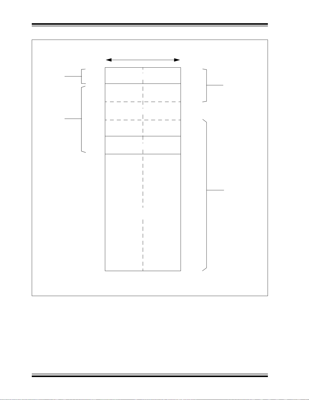
dsPIC33EPXXXGM3XX/6XX/7XX
0x0000
0x0FFE
0x7FFE
0xFFFE
LSB
Address
16 Bits
LSBMSB
MSB
Address
0x0001
0x0FFF
0x7FFF
0xFFFF
Optionally
Mapped
into Program
Memory Space
0xEFFF 0xEFFE
0x1001
0x1000
0x8001
0x8000
4-Kbyte
SFR Space
48-Kbyte
SRAM Space
0xD0000xD001
Space
Near Data
8-Kbyte
Note: Memory areas are not shown to scale.
(via PSV)
0x1FFE
0x1FFF
0x2001
0x2000
0x8FFE
0x8FFF
0x9001
0x9000
X Data
Unimplemented (X)
SFR Space
X Data RAM (X)
Y Data RAM (Y)
FIGURE 4-7: DATA MEMORY MAP FOR 512-KBYTE DEVICES
DS70000689D-page 44 2013-2014 Microchip Technology Inc.

dsPIC33EPXXXGM3XX/6XX/7XX
4.2.5 X AND Y DATA SPACES
The dsPIC33EP core has two Data Spaces: X and Y.
These Data Spaces can be considered either separate
(for some DSP instructions) or as one unified linear
address range (for MCU instructions). The Data
Spaces are accessed using two Address Generation
Units (AGUs) and separate data paths. This feature
allows certain instructions to concurrently fetch two
words from RAM, thereby enabling efficient execution
of DSP algorithms, such as Finite Impulse Response
(FIR) filtering and Fast Fourier Transform (FFT).
The X Data Space is used by all instructions and
supports all addressing modes. The X Data Space has
separate read and write data buses. The X read data
bus is the read data path for all instructions that view
Data Space as combined X and Y address space. It is
also the X data prefetch path for the dual operand DSP
instructions (MAC class).
The Y Data Space is used in concert with the X Data
Space by the MAC class of instructions (CLR, ED,
EDAC, MAC, MOVSAC, MPY, MPY.N and MSC) to provide
two concurrent data read paths.
Both the X and Y Data Spaces support Modulo
Addressing mode for all instructions, subject to
addressing mode restrictions. Bit-Reversed Addressing
mode is only supported for writes to X Data Space.
All data memory writes, including in DSP instructions,
view Data Space as combined X and Y address space.
The boundary between the X and Y Data Spaces is
device-dependent and is not user-programmable.
2013-2014 Microchip Technology Inc. DS70000689D-page 45
DS70000689D-page 46 2013-2014 Microchip Technology Inc.
4.3 Special Function Register Maps
dsPIC33EPXXXGM3XX/6XX/7XX
TABLE 4-1: CPU CORE REGISTER MAP
SFR
Name
W0 0000 W0 (WREG) xxxx
W1 0002 W1 xxxx
W2 0004 W2 xxxx
W3 0006 W3 xxxx
W4 0008 W4 xxxx
W5 000A W5 xxxx
W6 000C W6 xxxx
W7 000E W7 xxxx
W8 0010 W8 xxxx
W9 0012 W9 xxxx
W10 0014 W10 xxxx
W11 0016 W11 xxxx
W12 0018 W12 xxxx
W13 001A W13 xxxx
W14 001C W14 xxxx
W15 001E W15 xxxx
SPLIM 0020 SPLIM 0000
ACCAL 0022 ACCAL 0000
ACCAH 0024 ACCAH 0000
ACCAU 0026 Sign Extension of ACCA<39> ACCAU 0000
ACCBL 0028 ACCBL 0000
ACCBH 002A ACCBH 0000
ACCBU 002C Sign Extension of ACCB<39> ACCBU 0000
PCL 002E Program Counter Low Word Register
PCH 0030
DSRPAG 0032
DSWPAG 0034
RCOUNT 0036 REPEAT Loop Count Register 0000
DCOUNT 0038 DCOUNT<15:0> 0000
DOSTARTL 003A DOSTARTL<15:1>
DOSTARTH 003C
DOENDL 003E DOENDL<15:1>
DOENDH 0040
Legend: x = unknown value on Reset; — = unimplemented, read as ‘0’. Reset values are shown in hexadecimal.
Addr. Bit 15 Bit 14 Bit 13 Bit 12 Bit 11 Bit 10 Bit 9 Bit 8 Bit 7 Bit 6 Bit 5 Bit 4 Bit 3 Bit 2 Bit 1 Bit 0
— 0000
— — — — — — — — — Program Counter High Word Register 0000
— — — — — — Data Space Read Page Register 0001
— — — — — — — Data Space Write Page Register 0001
— 0000
— — — — — — — — — —DOSTARTH<5:0>0000
— 0000
— — — — — — — — — — DOENDH<5:0> 0000
All
Resets
2013-2014 Microchip Technology Inc. DS70000689D-page 47
TABLE 4-1: CPU CORE REGISTER MAP (CONTINUED)
SFR
Name
SR 0042 OA OB SA SB OAB SAB DA DC IPL2 IPL1 IPL0 RA N OV Z C 0000
CORCON 0044 VAR
MODCON 0046 XMODEN YMODEN
XMODSRT 0048 XMODSRT<15:0>
XMODEND 004A XMODEND<15:0>
YMODSRT 004C YMODSRT<15:0>
YMODEND 004E YMODEND<15:0>
XBREV 0050 BREN XBREV<14:0> 0000
DISICNT 0052
TBLPAG 0054
MSTRPR 0058 MSTRPR<15:0> 0000
Legend: x = unknown value on Reset; — = unimplemented, read as ‘0’. Reset values are shown in hexadecimal.
Addr. Bit 15 Bit 14 Bit 13 Bit 12 Bit 11 Bit 10 Bit 9 Bit 8 Bit 7 Bit 6 Bit 5 Bit 4 Bit 3 Bit 2 Bit 1 Bit 0
— US1 US0 EDT DL1 DL2 DL0 SATA SATB SATDW ACCSAT IPL3 SFA RND IF 0020
— — BWM3 BWM2 BWM1 BWM0 YWM3 YWM2 YWM1 YWM0 XWM3 XWM2 XWM1 XWM0 0000
— 0000
— 0001
— 0000
— 0001
— — DISICNT<13:0> 0000
— — — — — — — —TBLPAG<7:0>0000
All
Resets
dsPIC33EPXXXGM3XX/6XX/7XX

DS70000689D-page 48 2013-2014 Microchip Technology Inc.
dsPIC33EPXXXGM3XX/6XX/7XX
TABLE 4-2: INTERRUPT CONTROLLER REGISTER MAP FOR dsPIC33EPXXXGM6XX/7XX DEVICES
SFR
Addr. Bit 15 Bit 14 Bit 13 Bit 12 Bit 11 Bit 10 Bit 9 Bit 8 Bit 7 Bit 6 Bit 5 Bit 4 Bit 3 Bit 2 Bit 1 Bit 0
Name
INTCON1 08C0 NSTDIS OVAERR OVBERR COVAERR COVBERR OVATE OVBTE COVTE SFTACERR DIV0ERR DMACERR MATHERR ADDRERR STKERR OSCFAIL —
INTCON2 08C2 GIE DISI SWTRAP — — — — — — — — — — INT2EP INT1EP INT0EP
INTCON3 08C4 — — — — — — — — — — DAE DOOVR — — — —
INTCON4 08C6 — — — — — — — — — — — — — — —SGHT
IFS0 0800 — DMA1IF AD1IF U1TXIF U1RXIF SPI1IF SPI1EIF T3IF T2IF OC2IF IC2IF DMA0IF T1IF OC1IF IC1IF INT0IF
IFS1 0802 U2TXIF U2RXIF INT2IF T5IF T4IF OC4IF OC3IF DMA2IF IC8IF IC7IF AD2IF INT1IF CNIF CMPIF MI2C1IF SI2C1IF
IFS2 0804 T6IF —PMPIF
IFS3 0806 FLT1IF RTCCIF
IFS4 0808 — — CTMUIF FLT4IF QEI2IF FLT3IF PSESMIF — C2TXIF C1TXIF — — CRCIF U2EIF U1EIF FLT2IF
IFS5 080A PWM2IF PWM1IF — — SPI3IF SPI3EIF U4TXIF U4RXIF U4EIF — — — U3TXIF U3RXIF U3EIF —
IFS6 080C — — — — — — — — — — — — PWM6IF PWM5IF PWM4IF PWM3IF
IFS8 0810 JTAGIF ICDIF — — — — — — — — — — — — — —
IFS9 0812 — — — — — — — — — PTG3IF PTG2IF PTG1IF PTG0IF PTGWDTIF PTGSTEPIF —
IEC0 0820 — DMA1IE AD1IE U1TXIE U1RXIE SPI1IE SPI1EIE T3IE T2IE OC2IE IC2IE DMA0IE T1IE OC1IE IC1IE INT0IE
IEC1 0822 U2TXIE U2RXIE INT2IE T5IE T4IE OC4IE OC3IE DMA2IE IC8IE IC7IE AD2IE INT1IE CNIE CMPIE MI2C1IE SI2C1IE
IEC2 0824 T6IE —PMPIE
IEC3 0826 FLT1IE RTCCIE
IEC4 0828 — — CTMUIE FLT4IE QEI2I E FLT3IE PSESMIE — C2TXIE C1TXIE — — CRCIE U2EIE U1EIE FLT2IE
IEC5 082A PWM2IE PWM1IE — — SPI3IE SPI3EIE U4TXIE U4RXIE U4EIE — — — U3TXIE U3RXIE U3EIE —
IEC6 082C — — — — — — — — — — — — PWM6IE PWM5IE PWM4IE PWM3IE
IEC8 0830 JTAGIE ICDIE — — — — — — — — — — — — — —
IEC9 0832 — — — — — — — — — PTG3I E PTG2IE PTG1IE PTG0IE PTGWDTIE PTGSTEPIE —
IPC0 0840 — T1IP2 T1IP1 T1IP0 — OC1IP2 OC1IP1 OC1IP0 — IC1IP2 IC1IP1 IC1I P0 — INT0IP2 INT0IP1 INT0IP2
IPC1 0842 — T2IP2 T2IP1 T2IP0 — OC2IP2 OC2IP1 OC2IP0 — IC2IP2 IC2IP1 IC2I P0 — DMA0IP2 DMA0IP1 DMA0IP2
IPC2 0844 — U1RXIP2 U1RXIP1 U1RXIP0 — SPI1IP2 SPI1IP1 SPI1IP0 — SPI1EIP2 SPI1EIP1 SPI1EIP0 — T3IP2 T3IP1 T3IP0
IPC3 0846 — — — — — DMA1IP2 DMA1IP1 DMA1IP0 — AD1IP2 AD1IP1 AD1IP0 — U1TXIP2 U1TXIP1 U1TXIP0
IPC4 0848 — CNIP2 CNIP1 CNIP0 — CMPIP2 CMPIP1 CMPIP0 — MI2C1IP2 MI2C1IP1 MI2C1IP0 — SI2C1IP2 SI2C1IP1 SI2C1IP0
IPC5 084A — IC8IP2 IC8I P1 IC8IP0 — IC7IP2 IC7IP1 IC7IP0 — AD2IP2 AD2IP1 AD2IP0 — INT1IP2 INT1IP1 INT1IP0
IPC6 084C — T4IP2 T4IP1 T4IP0 — OC4IP2 OC4IP1 OC4IP0 — OC3IP2 OC3IP1 OC3IP0 — DMA2IP2 DMA2IP1 DMA2IP0
IPC7 084E — U2TXIP2 U2TXIP1 U2TXIP0 — U2RXIP2 U2RXIP1 U2RXIP0 — INT2IP2 INT2IP1 INT2IP0 — T5IP2 T5IP1 T5IP0
IPC8 0850 — C1IP2 C1IP1 C1IP0 — C1RXIP2 C1RXIP1 C1RXIP0 — SPI2IP2 SPI2IP1 SPI2IP0 — SPI2EIP2 SPI2EIP1 SPI2EIP0
IPC9 0852 — IC5IP2 I C5IP1 IC5IP0 — IC4IP2 IC4IP1 IC4IP0 — IC3IP2 I C3IP1 IC3IP0 — DMA3IP2 DMA3IP1 DMA3IP0
IPC10 0854 — OC7IP2 OC7I P1 OC7IP0 — OC6IP2 OC6IP1 OC6IP0 — OC5IP2 OC5IP1 OC5IP0 — IC6IP2 IC6IP1 IC6IP0
Legend:
Note 1:
— = unimplemented, read as ‘0’. Reset values are shown in hexadecimal.
The PMPIF/PMPIE/PMPIPx flags are not available on 44-pin devices.
2:
The RTCCIF/RTCCIE/RTCCIPx flags are not available on 44-pin devices.
(2)
(2)
(1)
OC8IF OC7IF OC6IF OC5IF IC6IF IC5IF IC4IF IC3IF DMA3IF C1IF C1RXIF SPI2IF SPI2EIF
— DCIIF DCIEIF QEI1IF PSEMIF C2IF C2RXIF INT4IF INT3IF T9IF T8IF MI2C2IF SI2C2IF T7IF
(1)
OC8IE OC7IE OC6IE OC5IE IC6IE IC5IE IC4IE IC3IE DMA3IE C1IE C1RXIE SPI2IE SPI2EIE
— DCIIE DCIEIE QEI1IE PSEMIE C2IE C2RXIE INT4IE INT3IE T9IE T8IE MI2C2IE SI2C2IE T7IE
All
Resets
0000
0000
0000
0000
0000
0000
0000
0000
0000
0000
0000
0000
0000
0000
0000
0000
0000
0000
0000
0000
0000
0000
4444
4444
4444
4444
4444
4444
4444
4444
4444
4444
4444

2013-2014 Microchip Technology Inc. DS70000689D-page 49
TABLE 4-2: INTERRUPT CONTROLLER REGISTER MAP FOR dsPIC33EPXXXGM6XX/7XX DEVICES (CONTINUED)
SFR
Addr. Bit 15 Bit 14 Bit 13 Bit 12 Bit 11 Bit 10 Bit 9 Bit 8 Bit 7 Bit 6 Bit 5 Bit 4 Bit 3 Bit 2 Bit 1 Bit 0
Name
IPC11 0856 — T6IP2 T6IP1 T6IP0 — — — — —PMPIP2
IPC12 0858 — T8IP2 T8IP1 T8IP0 — MI2C2IP2 MI2C2IP1 MI2C2IP0 — SI2C2IP2 SI2C2IP1 SI2C2IP0 — T7IP2 T7IP1 T7IP0
IPC13 085A — C2RXIP2 C2RXIP1 C2RXIP0 — INT4IP2 INT4IP1 INT4IP0 — INT3IP2 INT3IP1 INT3IP0 — T9IP2 T9IP1 T9IP0
IPC14 085C — DCIEIP2 DCIEI P1 DCIEIP0 — QEI1IP2 QEI1IP2 QEI1IP0 — PCEPIP2 PCEPIP1 PCEPIP0 — C2IP2 C2IP1 C2IP0
IPC15 085E — FLT1IP2 FLT1IP1 FLT1IP0 —RTCCIP2
IPC16 0860 — CRCIP2 CRCIP1 CRCIP0 — U2EIP2 U2EIP1 U2EIP0 — U1EIP2 U1EIP1 U1EIP0 — F LT2 IP2 FLT 2I P1 FLT 2I P0
IPC17 0862 — C2TXIP2 C2TXIP1 C2TXIP0 — C1TXIP2 C1TXIP1 C1TXIP0 — — — — — — — —
IPC18 0864 — QEI2IP2 QEI2IP1 QEI2IP0 — F LT3 IP 2 F LT3 I P1 F LT3 IP 0 — PCESIP2 PCESIP1 PCESIP0 — — — —
IPC19 0866 — — — — — — — — — CTMUIP2 CTMUIP1 CTMUIP0 — F LT4 IP2 FLT 4I P1 FLT 4I P0
IPC20 0868 — U3TXIP2 U3TXIP1 U3TXIP0 — U3RXIP2 U3RXIP1 U3RXIP0 — U3EIP2 U3EIP1 U3EIP0 — — — —
IPC21 086A — U4EIP2 U4EIP1 U4EIP0 — — — — — — — — — — — —
IPC22 086C — SPI3IP2 SPI3IP1 SPI3IP0 — SPI3EIP2 SPI3EIP1 SPI3EIP0 — U4TXIP2 U4TXIP1 U4TXIP0 — U4RXIP2 U4RXIP1 U4RXIP0
IPC23 086E — PGC2IP2 PGC2IP1 PGC2IP0 — PWM1IP2 PWM1IP1 PWM1IP0 — — — — — — — —
IPC24 0870 — PWM6IP2 PWM6IP1 PWM6IP0 — PWM5IP2 PWM5IP1 PWM5IP0 — PWM4IP2 PWM4IP1 PWM4IP0 — PWM3 IP2 PWM3 IP1 P WM3IP0
IPC35 0886 — JTAGIP2 JTAGIP1 JTAGIP0 — ICDIP2 ICDIP1 ICDIP0 — — — — — — — —
IPC36 0888 — PTG0IP2 PTG0IP1 PTG0IP0 — PTGWDTIP2 PTGWDTIP1 PTGWDTIP0 — PTGSTEPIP2 PTGSTEPIP1 PTGSTEPIP0 — — — —
IPC37 088A — — — — — PTG3IP2 PTG3IP1 PTG3IP0 — PTG2IP2 PTG2IP1 PTG2IP0 — PTG1IP2 PTG1IP1 PTG1IP0
INTTREG 08C8 — — — — ILR3 ILR2 ILR1 ILR0 VECNUM7 VECNUM6 VECNUM5 VECNUM4 VECNUM3 VECNUM2 VECNUM1 VECNUM0
Legend:
Note 1:
— = unimplemented, read as ‘0’. Reset values are shown in hexadecimal.
The PMPIF/PMPIE/PMPIPx flags are not available on 44-pin devices.
2:
The RTCCIF/RTCCIE/RTCCIPx flags are not available on 44-pin devices.
(2)
RTCCI P1
(2)
RTCCIP0
(2)
— — — — — DCIIP2 DCIIP1 DCIIP0
(1)
PMPIP1
(1)
PMPIP0
(1)
— OC8IP2 OC8IP1 OC8IP0
All
Resets
4444
4444
4444
4444
0404
4440
4400
4040
4000
0000
0000
0000
4400
4444
4400
4440
0445
0000
dsPIC33EPXXXGM3XX/6XX/7XX

DS70000689D-page 50 2013-2014 Microchip Technology Inc.
dsPIC33EPXXXGM3XX/6XX/7XX
TABLE 4-3: INTERRUPT CONTROLLER REGISTER MAP FOR dsPIC33EPXXXGM3XX DEVICES
SFR
Addr. Bit 15 Bit 14 Bit 13 Bit 12 Bit 11 Bit 10 Bit 9 Bit 8 Bit 7 Bit 6 Bit 5 Bit 4 Bit 3 Bit 2 Bit 1 Bit 0
Name
INTCON1 08C0 NSTDIS OVAERR OVBERR COVAERR COVBERR OVATE OVBTE COVTE SFTACERR DIV0ERR DMACERR MATHERR ADDRERR STKERR OSCFAIL —
INTCON2 08C2 GIE DISI SWTRAP — — — — — — — — — — INT2EP INT1EP INT0EP
INTCON3 08C4 — — — — — — — — — — DAE DOOVR — — — —
INTCON4 08C6 — — — — — — — — — — — — — — —SGHT
IFS0 0800 — DMA1IF AD1IF U1TXIF U1RXIF SPI1IF SPI1EIF T3IF T2IF OC2IF IC2IF DMA0IF T1IF OC1IF IC1IF INT0IF
IFS1 0802 U2TXIF U2RXIF INT2IF T5IF T4IF OC4IF OC3IF DMA2IF IC8IF IC7IF AD2IF INT1IF CNIF CMPIF MI2C1IF SI2C1IF
IFS2 0804 T6IF —PMPIF
IFS3 0806 FLT1IF RTCCIF
IFS4 0808 — — CTMUIF FLT4IF QEI2IF FLT3IF PSESMIF — — — — — CRCIF U2EIF U1EIF FLT2IF
IFS5 080A PWM2IF PWM1IF — — SPI3IF SPI3EIF U4TXIF U4RXIF U4EIF — — — U3TXIF U3RXIF U3EIF —
IFS6 080C — — — — — — — — — — — — PWM6IF PWM5IF PWM4I F PWM3IF
IFS8 0810 JTAGIF ICDIF — — — — — — — — — — — — — —
IFS9 0812 — — — — — — — — — PTG3IF PTG2IF PTG1IF PTG0IF PTGWDTIF PTGSTEPIF —
IEC0 0820 — DMA1IE AD1IE U1TXIE U1RXIE SPI1IE SPI1EIE T3IE T2IE OC2IE IC2IE DMA0IE T1IE OC1IE IC1IE INT0IE
IEC1 0822 U2TXIE U2RXIE INT2IE T5IE T4IE OC4IE OC3IE DMA2IE IC8IE IC7IE AD2IE INT1IE CNIE CMPIE MI2C1IE SI2C1IE
IEC2 0824 T6IE —PMPIE
IEC3 0826 FLT1IE RTCCIE
IEC4 0828 — — CTMUIE FLT4IE QEI2IE FLT3IE PSESMIE — — — — — CRCIE U2EIE U1EIE FLT2IE
IEC5 082A PWM2IE PWM1I E — — SPI3IE SPI3EIE U4TXIE U4RXIE U4EIE — — — U3TXIE U3RXIE U3EIE —
IEC6 082C — — — — — — — — — — — — PW M6IE PWM5IE PWM4I E PWM3I E
IEC8 0830 JTAGIE ICDIE — — — — — — — — — — — — — —
IEC9 0832 — — — — — — — — — PTG3IE PTG2IE PTG1IE PTG0IE PTGWDTIE PTGSTEPIE —
IPC0 0840 — T1IP2 T1IP1 T1IP0 — OC1IP2 OC1IP1 OC1IP0 — IC1IP2 IC1IP1 IC1IP0 — INT0IP2 INT0IP1 INT0IP2
IPC1 0842 — T2IP2 T2IP1 T2IP0 — OC2IP2 OC2IP1 OC2IP0 — IC2IP2 IC2IP1 IC2IP0 — DMA0IP2 DMA0IP1 DMA0IP2
IPC2 0844 — U1RXIP2 U1RXIP1 U1RXIP0 — SPI1IP2 SPI1IP1 SPI1IP0 — SPI1EIP2 SPI1EIP1 SPI1EIP0 — T3IP2 T3IP1 T3IP0
IPC3 0846 — — — — — DMA1IP2 DMA1IP1 DMA1IP0 — AD1IP2 AD1IP1 AD1IP0 — U1TXIP2 U1TXIP1 U1TXIP0
IPC4 0848 — CNIP2 CNIP1 CNIP0 — CMPIP2 CMPIP1 CMPIP0 — MI2C1IP2 MI2C1IP1 MI2C1IP0 — SI2C1IP2 SI2C1IP1 SI2C1IP0
IPC5 084A — IC8IP2 I C8IP1 IC8IP0 — IC7IP2 IC7IP1 IC7IP0 — AD2IP2 AD2IP1 AD2IP0 — INT1IP2 INT1IP1 INT1IP0
IPC6 084C — T4IP2 T4IP1 T4IP0 — OC4IP2 OC4IP1 OC4IP0 — OC3IP2 OC3IP1 OC3IP0 — DMA2IP2 DMA2IP1 DMA2IP0
IPC7 084E — U2TXIP2 U2TXIP1 U2TXIP0 — U2RXIP2 U2RXIP1 U2RXIP0 — INT2IP2 INT2IP1 INT2IP0 — T5IP2 T5IP1 T5IP0
IPC8 0850 — — — — — — — SPI2IP2 SPI2IP1 SPI2IP0 — SPI2EIP2 SPI2EIP1 SPI2EIP0
IPC9 0852 — IC5IP2 IC5IP1 IC5IP0 — IC4IP2 IC4IP1 IC4IP0 — IC3IP2 IC3IP1 IC3IP0 — DMA3IP2 DMA3IP1 DMA3IP0
IPC10 0854 — OC7IP2OC7IP1OC7IP0 — OC6IP2 OC6IP1 OC6IP0 — OC5IP2 OC5IP1 OC5IP0 — IC6IP2 IC6IP1 IC6IP0
Legend:
Note 1:
— = unimplemented, read as ‘0’. Reset values are shown in hexadecimal.
The PMPIF/PMPIE/PMPIPx flags are not available on 44-pin devices.
2:
The RTCCIF/RTCCIE/RTCCIPx flags are not available on 44-pin devices.
(2)
(2)
(1)
OC8IF OC7IF OC6IF OC5IF IC6IF IC5IF IC4IF IC3IF DMA3IF — —SPI2IFSPI2EIF
— DCIIF DCIEIF QEI1IF PSEMIF — — INT4IF INT3IF T9IF T8IF MI2C2IF SI2C2IF T7IF
(1)
OC8IE OC7IE OC6IE OC5IE IC6IE IC5IE IC4IE IC3IE DMA3IE — —SPI2IESPI2EIE
— DCIIE DCIEIE QEI1IE PSEMIE — — INT4IE INT3IE T9IE T8IE MI2C2IE SI2C2IE T7IE
All
Resets
0000
0000
0000
0000
0000
0000
0000
0000
0000
0000
0000
0000
0000
0000
0000
0000
0000
0000
0000
0000
0000
0000
4444
4444
4444
4444
4444
4444
4444
4444
4444
4444
4444

2013-2014 Microchip Technology Inc. DS70000689D-page 51
TABLE 4-3: INTERRUPT CONTROLLER REGISTER MAP FOR dsPIC33EPXXXGM3XX DEVICES (CONTINUED)
SFR
Addr. Bit 15 Bit 14 Bit 13 Bit 12 Bit 11 Bit 10 Bit 9 Bit 8 Bit 7 Bit 6 Bit 5 Bit 4 Bit 3 Bit 2 Bit 1 Bit 0
Name
IPC11 0856 — T6IP2 T6IP1 T6IP0 — — — — —PMPIP2
IPC12 0858 — T8IP2 T8IP1 T8IP0 — MI2C2IP2 MI2C2IP1 MI2C2IP0 — SI2C2IP2 SI2C2IP1 SI2C2IP0 — T7IP2 T7IP1 T7IP0
IPC13 085A — — — — — INT4IP2 INT4IP1 INT4IP0 — INT3IP2 INT3IP1 INT3IP0 — T9IP2 T9IP1 T9IP0
IPC14 085C — DCIEIP2 DCIEIP1 DCIEIP0 — QEI1IP2 QEI1IP2 QEI1IP0 — PCEPIP2 PCEPIP1 PCEPIP0 — — — —
IPC15 085E — FLT 1I P2 FL T1 IP 1 F LT 1I P 0 —RTCCIP2
IPC16 0860 — CRCIP2 CRCIP1 CRCIP0 — U2EIP2 U2EIP1 U2EIP0 — U1EIP2 U1EIP1 U1EIP0 — FLT2IP2 FLT2IP1 FLT2IP0
IPC18 0864 — C2TXIP2 C2TXIP1 C2TXIP0 — FLT3IP2 FLT3IP1 FLT3IP0 — PCESIP2 PCESIP1 PCESIP0 — — — —
IPC19 0866 — — — — — — — — — CTMUIP2 CTMUIP1 CTMUIP0 — FLT4IP2 FLT4IP1 FLT4IP0
IPC20 0868 — U3TXIP2 U3TXIP1 U3TXIP0 — U3RXIP2 U3RXIP1 U3RXIP0 — U3EIP2 U3EIP1 U3EIP0 — — — —
IPC21 086A — U4EIP2 U4EIP1 U4EIP0 — — — — — — — — — — — —
IPC22 086C — SPI3IP2 SPI3IP1 SPI3IP0 — SPI3EIP2 SPI3EIP1 SPI3EIP0 — U4TXIP2 U4TXIP1 U4TXIP0 — U4RXIP2 U4RXIP1 U4RXIP0
IPC23 086E — PGC2IP2 PGC2IP1 PGC2IP0 — PWM1IP2 PWM1IP1 PWM1IP0 — — — — — — — —
IPC24 0870 — PWM6IP2 PWM6IP1 PWM6IP0 — PWM5IP2 PWM5IP1 PWM5IP0 — PWM4IP2 PWM4I P1 PWM4IP0 — PWM3IP2 PWM3IP1 PWM3IP0
IPC35 0886 — JTA GIP 2 J TAG IP1 JTAG IP0 — ICDIP2 ICDIP1 ICDIP0 — — — — — — — —
IPC36 0888 — PTG0IP2 PTG0IP1 PTG0IP0 — PTGWDTI P2 PTGWDTIP1 PTGWDTIP0 — PTGSTEPIP2 PTGSTEPIP1 PTGSTEPIP0 — — — —
IPC37 088A — — — — — PTG3IP2 PTG3IP1 PTG3IP0 — PTG2IP2 PTG2IP1 PTG2IP0 — PTG1IP2 PTG1IP1 PTG1IP0
INTTREG 08C8 — — — — ILR3 ILR2 ILR1 ILR0 VECNUM7 VECNUM6 VECNUM5 VECNUM4 VECNUM3 VECNUM2 VECNUM1 VECNUM0
Legend:
Note 1:
— = unimplemented, read as ‘0’. Reset values are shown in hexadecimal.
The PMPIF/PMPIE/PMPIPx flags are not available on 44-pin devices.
2:
The RTCCIF/RTCCIE/RTCCIPx flags are not available on 44-pin devices.
(2)
RTCCIP1
(2)
RTCCIP0
(2)
— — — — — DCIIP2 DCIIP1 DCIIP0
(1)
PMPIP1
(1)
PMPIP0
(1)
— OC8IP2 OC8IP1 OC8IP0
All
Resets
4444
4444
4444
4444
0404
4440
4040
0004
0000
0000
0000
4400
4444
4400
4440
0444
0000
dsPIC33EPXXXGM3XX/6XX/7XX

DS70000689D-page 52 2013-2014 Microchip Technology Inc.
dsPIC33EPXXXGM3XX/6XX/7XX
TABLE 4-4: TIMERS REGISTER MAP
SFR
Name
TMR1 0100 Timer1 Register 0000
PR1 0102 Period Register 1 FFFF
T1CON 0104 TON
TMR2 0106 Timer2 Register 0000
TMR3HLD 0108 Timer3 Holding Register (For 32-bit timer operations only) xxxx
TMR3 010A Timer3 Register 0000
PR2 010C Period Register 2 FFFF
PR3 010E Period Register 3 FFFF
T2CON 0110 TON
T3CON 0112 TON
TMR4 0114 Timer4 Register 0000
TMR5HLD 0116 Timer5 Holding Register (For 32-bit timer operations only) xxxx
TMR5 0118 Timer5 Register 0000
PR4 011A Period Register 4 FFFF
PR5 011C Period Register 5 FFFF
T4CON 011E TON
T5CON 0120 TON
TMR6 0122 Timer6 Register 0000
TMR7HLD 0124 Timer7 Holding Register (For 32-bit timer operations only) xxxx
TMR7 0126 Timer7 Register 0000
PR6 0128 Period Register 6 FFFF
PR7 012A Period Register 7 FFFF
T6CON 012C TON
T7CON 012E TON
TMR8 0130 Timer8 Register 0000
TMR9HLD 0132 Timer9 Holding Register (For 32-bit timer operations only) xxxx
TMR9 0134 Timer9 Register 0000
PR8 0136 Period Register 8 FFFF
PR9 0138 Period Register 9 FFFF
T8CON 013A TON
T9CON 013C TON
Legend: x = unknown value on Reset; — = unimplemented, read as ‘0’. Reset values are shown in hexadecimal.
Addr. Bit 15 Bit 14 Bit 13 Bit 12 Bit 11 Bit 10 Bit 9 Bit 8 Bit 7 Bit 6 Bit 5 Bit 4 Bit 3 Bit 2 Bit 1 Bit 0
—TSIDL — — — — — — TGATE TCKPS1 TCKPS0 — TSYNC TCS — 0000
—TSIDL — — — — — — TGATE TCKPS1 TCKPS0 T32 —TCS — 0000
—TSIDL — — — — — — TGATE TCKPS1 TCKPS0 — —TCS — 0000
—TSIDL — — — — — — TGATE TCKPS1 TCKPS0 T32 —TCS — 0000
—TSIDL — — — — — — TGATE TCKPS1 TCKPS0 — —TCS — 0000
—TSIDL — — — — — — TGATE TCKPS1 TCKPS0 T32 —TCS — 0000
—TSIDL — — — — — — TGATE TCKPS1 TCKPS0 — —TCS — 0000
—TSIDL — — — — — — TGATE TCKPS1 TCKPS0 T32 —TCS — 0000
—TSIDL — — — — — — TGATE TCKPS1 TCKPS0 — —TCS — 0000
All
Resets

2013-2014 Microchip Technology Inc. DS70000689D-page 53
TABLE 4-5: INPUT CAPTURE 1 THROUGH INPUT CAPTURE 8 REGISTER MAP
SFR
Name
IC1CON1 0140
IC1CON2 0142
IC1BUF 0144 Input Capture 1 Buffer Register xxxx
IC1TMR 0146 Input Capture 1 Timer Register 0000
IC2CON1 0148
IC2CON2 014A
IC2BUF 014C Input Capture 2 Buffer Register xxxx
IC2TMR 014E Input Capture 2 Timer Register 0000
IC3CON1 0150
IC3CON2 0152
IC3BUF 0154 Input Capture 3 Buffer Register xxxx
IC3TMR 0156 Input Capture 3 Timer Register 0000
IC4CON1 0158
IC4CON2 015A
IC4BUF 015C Input Capture 4 Buffer Register xxxx
IC4TMR 015E Input Capture 4 Timer Register 0000
IC5CON1 0160
IC5CON2 0162
IC5BUF 0164 Input Capture 5 Buffer Register xxxx
IC5TMR 0166 Input Capture 5 Timer Register 0000
IC6CON1 0168
IC6CON2 016A
IC6BUF 016C Input Capture 6 Buffer Register xxxx
IC6TMR 016E Input Capture 6 Timer Register 0000
IC7CON1 0170
IC7CON2 0172
IC7BUF 0174 Input Capture 7 Buffer Register xxxx
IC7TMR 0176 Input Capture 7 Timer Register 0000
IC8CON1 0178
IC8CON2 017A
IC8BUF 017C Input Capture 8 Buffer Register xxxx
IC8TMR 017E Input Capture 8 Timer Register 0000
Legend: x = unknown value on Reset; — = unimplemented, read as ‘0’. Reset values are shown in hexadecimal.
Addr. Bit 15 Bit 14 Bit 13 Bit 12 Bit 11 Bit 10 Bit 9 Bit 8 Bit 7 Bit 6 Bit 5 Bit 4 Bit 3 Bit 2 Bit 1 Bit 0
— — ICSIDL ICTSEL2 ICTSEL1 ICTSEL0 — — — ICI1 ICI0 ICOV ICBNE ICM2 ICM1 ICM0 0000
— — — — — — — IC32 ICTRIG TRIGSTAT — SYNCSEL4 SYNCSEL3 SYNCSEL2 SYNCSEL1 SYNCSEL0 000D
— — ICSIDL ICTSEL2 ICTSEL1 ICTSEL0 — — — ICI1 ICI0 ICOV ICBNE ICM2 ICM1 ICM0 0000
— — — — — — — IC32 ICTRIG TRIGSTAT — SYNCSEL4 SYNCSEL3 SYNCSEL2 SYNCSEL1 SYNCSEL0 000D
— — ICSIDL ICTSEL2 ICTSEL1 ICTSEL0 — — — ICI1 ICI0 ICOV ICBNE ICM2 ICM1 ICM0 0000
— — — — — — — IC32 ICTRIG TRIGSTAT — SYNCSEL4 SYNCSEL3 SYNCSEL2 SYNCSEL1 SYNCSEL0 000D
— — ICSIDL ICTSEL2 ICTSEL1 ICTSEL0 — — — ICI1 ICI0 ICOV ICBNE ICM2 ICM1 ICM0 0000
— — — — — — — IC32 ICTRIG TRIGSTAT — SYNCSEL4 SYNCSEL3 SYNCSEL2 SYNCSEL1 SYNCSEL0 000D
— — ICSIDL ICTSEL2 ICTSEL1 ICTSEL0 — — — ICI1 ICI0 ICOV ICBNE ICM2 ICM1 ICM0 0000
— — — — — — — IC32 ICTRIG TRIGSTAT — SYNCSEL4 SYNCSEL3 SYNCSEL2 SYNCSEL1 SYNCSEL0 000D
— — ICSIDL ICTSEL2 ICTSEL1 ICTSEL0 — — — ICI1 ICI0 ICOV ICBNE ICM2 ICM1 ICM0 0000
— — — — — — — IC32 ICTRIG TRIGSTAT — SYNCSEL4 SYNCSEL3 SYNCSEL2 SYNCSEL1 SYNCSEL0 000D
— — ICSIDL ICTSEL2 ICTSEL1 ICTSEL0 — — — ICI1 ICI0 ICOV ICBNE ICM2 ICM1 ICM0 0000
— — — — — — — IC32 ICTRIG TRIGSTAT — SYNCSEL4 SYNCSEL3 SYNCSEL2 SYNCSEL1 SYNCSEL0 000D
— — ICSIDL ICTSEL2 ICTSEL1 ICTSEL0 — — — ICI1 ICI0 ICOV ICBNE ICM2 ICM1 ICM0 0000
— — — — — — — IC32 ICTRIG TRIGSTAT — SYNCSEL4 SYNCSEL3 SYNCSEL2 SYNCSEL1 SYNCSEL0 000D
All
Resets
dsPIC33EPXXXGM3XX/6XX/7XX

DS70000689D-page 54 2013-2014 Microchip Technology Inc.
dsPIC33EPXXXGM3XX/6XX/7XX
TABLE 4-6: OUTPUT COMPARE REGISTER MAP
SFR
Name
OC1CON1 0900
OC1CON2 0902 FLTMD FLTOUT FLTTRIEN OCINV
OC1RS 0904 Output Compare 1 Secondary Register xxxx
OC1R 0906 Output Compare 1 Register xxxx
OC1TMR 0908 Output Compare 1 Timer Value Register xxxx
OC2CON1 090A
OC2CON2 090C FLTMD FLTOUT FLTTRIEN OCINV
OC2RS 090E Output Compare 2 Secondary Register xxxx
OC2R 0910 Output Compare 2 Register xxxx
OC2TMR 0912 Output Compare 2 Timer Value Register xxxx
OC3CON1 0914
OC3CON2 0916 FLTMD FLTOUT FLTTRIEN OCINV
OC3RS 0918 Output Compare 3 Secondary Register xxxx
OC3R 091A Output Compare 3 Register xxxx
OC3TMR 091C Output Compare 3 Timer Value Register xxxx
OC4CON1 091E
OC4CON2 0920 FLTMD FLTOUT FLTTRIEN OCINV
OC4RS 0922 Output Compare 4 Secondary Register xxxx
OC4R 0924 Output Compare 4 Register xxxx
OC4TMR 0926 Output Compare 4 Timer Value Register xxxx
OC5CON1 0928
OC5CON2 092A FLTMD FLTOUT FLTTRIEN OCINV
OC5RS 092C Output Compare 5 Secondary Register xxxx
OC5R 092E Output Compare 5 Register xxxx
OC5TMR 0930 Output Compare 5 Timer Value Register xxxx
OC6CON1 0932
OC6CON2 0934 FLTMD FLTOUT FLTTRIEN OCINV
OC6RS 0936 Output Compare 6 Secondary Register xxxx
OC6R 0938 Output Compare 6 Register xxxx
OC6TMR 093A Output Compare 6 Timer Value Register xxxx
Legend: x = unknown value on Reset; — = unimplemented, read as ‘0’. Reset values are shown in hexadecimal.
Addr. Bit 15 Bit 14 Bit 13 Bit 12 Bit 11 Bit 10 Bit 9 Bit 8 Bit 7 Bit 6 Bit 5 Bit 4 Bit 3 Bit 2 Bit 1 Bit 0
— — OCSIDL OCTSEL2 OCTSEL1 OCTSEL0 — ENFLTB ENFLTA — OCFLTB OCFLTA TRIGMODE OCM2 OCM1 OCM0 0000
— — — OC32 OCTRIG TRIGSTAT O CTRIS SYNCSEL4 SYNCSEL3 SYNCSEL2 SYNCSEL1 SYNCSEL0 000C
— — OCSIDL OCTSEL2 OCTSEL1 OCTSEL0 — ENFLTB ENFLTA — OCFLTB OCFLTA TRIGMODE OCM2 OCM1 OCM0 0000
— — — OC32 OCTRIG TRIGSTAT O CTRIS SYNCSEL4 SYNCSEL3 SYNCSEL2 SYNCSEL1 SYNCSEL0 000C
— — OCSIDL OCTSEL2 OCTSEL1 OCTSEL0 — ENFLTB ENFLTA — OCFLTB OCFLTA TRIGMODE OCM2 OCM1 OCM0 0000
— — — OC32 OCTRIG TRIGSTAT O CTRIS SYNCSEL4 SYNCSEL3 SYNCSEL2 SYNCSEL1 SYNCSEL0 000C
— — OCSIDL OCTSEL2 OCTSEL1 OCTSEL0 — ENFLTB ENFLTA — OCFLTB OCFLTA TRIGMODE OCM2 OCM1 OCM0 0000
— — — OC32 OCTRIG TRIGSTAT O CTRIS SYNCSEL4 SYNCSEL3 SYNCSEL2 SYNCSEL1 SYNCSEL0 000C
— — OCSIDL OCTSEL2 OCTSEL1 OCTSEL0 — ENFLTB ENFLTA — OCFLTB OCFLTA TRIGMODE OCM2 OCM1 OCM0 0000
— — — OC32 OCTRIG TRIGSTAT O CTRIS SYNCSEL4 SYNCSEL3 SYNCSEL2 SYNCSEL1 SYNCSEL0 000C
— — OCSIDL OCTSEL2 OCTSEL1 OCTSEL0 — ENFLTB ENFLTA — OCFLTB OCFLTA TRIGMODE OCM2 OCM1 OCM0 0000
— — — OC32 OCTRIG TRIGSTAT O CTRIS SYNCSEL4 SYNCSEL3 SYNCSEL2 SYNCSEL1 SYNCSEL0 000C
All
Resets
2013-2014 Microchip Technology Inc. DS70000689D-page 55
TABLE 4-6: OUTPUT COMPARE REGISTER MAP (CONTINUED)
SFR
Name
OC7CON1 093C — — OCSIDL OCTSEL2 OCTSEL1 OCTSEL0 — ENFLTB ENFLTA — OCFLTB OCFLTA TRIGMODE OCM2 OCM1 OCM0 0000
OC7CON2 093E FLTMD FLTOUT FLTTRIEN OCINV
OC7RS 0940 Output Compare 7 Secondary Register xxxx
OC7R 0942 Output Compare 7 Register xxxx
OC7TMR 0944 Output Compare 7 Timer Value Register xxxx
OC8CON1 0946
OC8CON2 0948 FLTMD FLTOUT FLTTRIEN OCINV
OC8RS 094A Output Compare 8 Secondary Register xxxx
OC8R 094C Output Compare 8 Register xxxx
OC8TMR 094E Output Compare 8 Timer Value Register xxxx
Legend: x = unknown value on Reset; — = unimplemented, read as ‘0’. Reset values are shown in hexadecimal.
Addr. Bit 15 Bit 14 Bit 13 Bit 12 Bit 11 Bit 10 Bit 9 Bit 8 Bit 7 Bit 6 Bit 5 Bit 4 Bit 3 Bit 2 Bit 1 Bit 0
— — — OC32 OCTRIG TRIGSTAT O CTRIS SYNCSEL4 SYNCSEL3 SYNCSEL2 SYNCSEL1 SYNCSEL0 000C
— — OCSIDL OCTSEL2 OCTSEL1 OCTSEL0 — ENFLTB ENFLTA — OCFLTB OCFLTA TRIGMODE OCM2 OCM1 OCM0 0000
— — — OC32 OCTRIG TRIGSTAT O CTRIS SYNCSEL4 SYNCSEL3 SYNCSEL2 SYNCSEL1 SYNCSEL0 000C
All
Resets
dsPIC33EPXXXGM3XX/6XX/7XX

DS70000689D-page 56 2013-2014 Microchip Technology Inc.
dsPIC33EPXXXGM3XX/6XX/7XX
TABLE 4-7: PTG REGISTER MAP
SFR
Name
PTGCST 0AC0 PTGEN — PTGSIDL PTGTOGL — PTGSWT PTGSSEN PTGIVIS PTGSTRT PTGWDTO — — — — PTGITM1 PTGITM0
PTGCON 0AC2 PTGCLK2 PTGCLK1 PTGCLK0 PTGDIV4 PTGDIV3 PTGDIV2 PTGDIV1 PTGDIV0 PTGPWD3 PTGPWD2 PTGPWD1 PTGPWD0 — PTGWDT2 PTGWDT1 PTGWDT0
PTGBTE 0AC4 ADCTS4 ADCTS3 ADCTS2 ADCTS1 IC4TSS IC3TSS IC2TSS IC1TSS OC4CS OC3CS OC2CS OC1CS OC4TSS OC3TSS OC2TSS OC1TSS
PTGHOLD 0AC6 PTGHOLD<15:0>
PTGT0LIM 0AC8 PTGT0LIM<15:0>
PTGT1LIM 0ACA PTGT1LIM<15:0>
PTGSDLIM 0ACC PTGSDLIM<15:0>
PTGC0LIM 0ACE PTGC0LIM<15:0>
PTGC1LIM 0AD0 PTGC1LIM<15:0>
PTGADJ 0AD2 PTGADJ<15:0>
PTGL0 0AD4 PTGL0<15:0>
PTGQPTR 0AD6 — — — — — — — — — — — PTGQPTR<4:0>
PTGQUE0 0AD8 STEP1<7:0> STEP0<7:0>
PTGQUE1 0ADA STEP3<7:0> STEP2<7:0>
PTGQUE2 0ADC STEP5<7:0> STEP4<7:0>
PTGQUE3 0ADE STEP7<7:0> STEP6<7:0>
PTGQUE4 0AE0 STEP9<7:0> STEP8<7:0>
PTGQUE5 0AE2 STEP11<7:0> STEP10<7:0>
PTGQUE6 0AE4 STEP13<7:0> STEP12<7:0>
PTGQUE7 0AE6 STEP15<7:0> STEP14<7:0>
PTGQUE8 0x0AE8 STEP17<7:0> STEP16<7:0>
PTGQUE9 0x0AEA STEP19<7:0> STEP18<7:0>
PTGQUE10 0x0AEC STEP21<7:0> STEP20<7:0>
PTGQUE11 0x0AEE STEP23<7:0> STEP22<7:0>
PTGQUE12 0x0AF0 STEP25<7:0> STEP24<7:0>
PTGQUE13 0x0AF2 STEP27<7:0> STEP26<7:0>
PTGQUE14 0x0AF4 STEP29<7:0> STEP28<7:0>
PTGQUE15 0x0AF6 STEP31<7:0> STEP30<7:0>
Legend:
Addr. Bit 15 Bit 14 Bit 13 Bit 12 Bit 11 Bit 10 Bit 9 Bit 8 Bit 7 Bit 6 Bit 5 Bit 4 Bit 3 Bit 2 Bit 1 Bit 0
x
= unknown value on Reset; — = unimplemented, read as ‘0’. Reset values are shown in hexadecimal.
All
Resets
0000
0000
0000
0000
0000
0000
0000
0000
0000
0000
0000
0000
0000
0000
0000
0000
0000
0000
0000
0000
0000
0000
0000
0000
0000
0000
0000
0000

2013-2014 Microchip Technology Inc. DS70000689D-page 57
TABLE 4-8: PWM REGISTER MAP
SFR
Name
PTCON 0C00 PTEN — PTSIDL SESTAT SEIEN EIPU SYNCPOL SYNCOEN SYNCEN SYNCSRC2 SYNCSRC1 SYNCSRC0 SEVTPS3 SEVTPS2 SEVTPS1 SEVTPS0
PTCON2 0C02 — — — — — — — — — — — — —PCLKDIV<2:0>
PTPER 0C04 PTPER<15:0>
SEVTCMP 0C06 SEVTCMP<15:0>
MDC 0C0A MDC<15:0>
STCON 0C0E — — — SESTAT SEIEN EIPU SYNCPOL SYNCOEN SYNCEN SYNCSRC2 SYNCSRC1 SYNCSRC0 SEVTPS3 SEVTPS2 SEVTPS1 SEVTPS0
STCON2 0C10 — — — — — — — — — — — — —PCLKDIV<2:0>
STPER 0C12 STPER<15:0>
SSEVTCMP 0C14 SSEVTCMP<15:0>
CHOP 0C1A CHPCLKEN — — — — — CHOPCLK9 CHOPCLK8 CHOPCLK7 CHOPCLK6 CHOPCLK5 CHOPCLK4 CHOPCLK3 CHOPCLK2 CHOPCLK1 CHOPCLK0
PWMKEY 0C1E PWMKEY<15:0>
Legend:
Addr. Bit 15 Bit 14 Bit 13 Bit 12 Bit 11
— = unimplemented, read as ‘0’. Reset values are shown in hexadecimal.
Bit
Bit 9 Bit 8 Bit 7 Bit 6 Bit 5 Bit 4 Bit 3 Bit 2 Bit 1 Bit 0
10
Resets
TABLE 4-9: PWM GENERATOR 1 REGISTER MAP
SFR
Addr. Bit 15 Bit 14 Bit 13 Bit 12 Bit 11 Bit 10 Bit 9 Bit 8 Bit 7 Bit 6 Bit 5 Bit 4 Bit 3 Bit 2 Bit 1 Bit 0
Name
PWMCON1 0C20 FLTSTAT CLSTAT TRGSTAT FLTIEN CLIEN TRGIEN ITB MDCS DTC1 DTC0 DTCP — MTBS CAM XPRES IUE
IOCON1 0C22 PENH PENL POLH POLL PMOD1 PMOD0 OVRENH OVRENL OVRDAT1 OVRDAT0 FLTDAT1 FLTDAT0 CLDAT1 CLDAT0 SWAP OSYNC
FCLCON1 0C24 IFLTMOD CLSRC4 CLSRC3 CLSRC2 CLSRC1 CLSRC0 CLPOL CLMOD FLTSRC4 FLTSRC3 FLTSRC2 FLTSRC1 FLTSRC0 FLTPOL FLTMOD1 FLTMOD0
PDC1 0C26 PDC1<15:0>
PHASE1 0C28 PHASE1<15:0>
DTR1 0C2A — — DTR1<13:0>
ALTDTR1 0C2C — — ALTDTR1<13:0>
SDC1 0C2E SDC1<15:0>
SPHASE1 0C30 SPHASE1<15:0>
TRIG1 0C32 TRGCMP<15:0>
TRGCON1 0C34 TRGDIV3 TRGDIV2 TRGDIV1 TRGDIV0 — — — — — — TRGSTRT5 TRGSTRT4 TRGSTRT3 TRGSTRT2 TRGSTRT1 TRGSTRT0
PWMCAP1 0C38 PWMCAP1<15:0>
LEBCON1 0C3A PHR PHF PLR PLF FLTLEBEN CLLEBEN — — — — BCH BCL BPHH BPHL BPLH BPLL
LEBDLY1 0C3C — — — — LEB<11:0>
AUXCON1 0C3E — — — — BLANKSEL3 BLANKSEL2 BLANKSEL1 BLANKSEL0 — — CHOPSEL3 CHOPSEL2 CHOPSEL1 CHOPSEL0 CHOPHEN CHOPLEN
Legend:
— = unimplemented, read as ‘0’. Reset values are shown in hexadecimal.
Resets
All
0000
0000
00F8
0000
0000
0000
0000
0000
0000
0000
0000
dsPIC33EPXXXGM3XX/6XX/7XX
All
0000
C000
0000
FFF8
0000
0000
0000
0000
0000
0000
0000
0000
0000
0000
0000

DS70000689D-page 58 2013-2014 Microchip Technology Inc.
TABLE 4-10: PWM GENERATOR 2 REGISTER MAP
SFR
Addr. Bit 15 Bit 14 Bit 13 Bit 12 Bit 11 Bit 10 Bit 9 Bit 8 Bit 7 Bit 6 Bit 5 Bit 4 Bit 3 Bit 2 Bit 1 Bit 0
Name
PWMCON2 0C40 FLTSTAT CLSTAT TRGSTAT FLTIEN CLIEN TRGIEN ITB MDCS DTC1 DTC0 DTCP — MTBS CAM XPRES IUE
IOCON2 0C42 PENH PENL POLH POLL PMOD1 PMOD0 OVRENH OVRENL OVRDAT1 OVRDAT0 FLTDAT1 FLTDAT0 CLDAT1 CLDAT0 SWAP OSYNC
FCLCON2 0C44 IFLTMOD CLSRC4 CLSRC3 CLSRC2 CLSRC1 CLSRC0 CLPOL CLMOD FLTSRC4 FLTSRC3 FLTSRC2 FLTSRC1 FLTSRC0 FLTPOL FLTMOD1 FLTMOD0
PDC2 0C46 PDC2<15:0>
PHASE2 0C48 PHASE2<15:0>
DTR2 0C4A — — DTR2<13:0>
ALTDTR2 0C4C — — ALTDTR2<13:0>
SDC2 0C4E SDC2<15:0>
SPHASE2 0C50 SPHASE2<15:0>
TRIG2 0C52 TRGCMP<15:0>
TRGCON2 0C54 TRGDIV3 TRGDIV2 TRGDIV1 TRGDIV0 — — — — — — TRGSTRT5 TRGSTRT4 TRGSTRT3 TRGSTRT2 TRGSTRT1 TRGSTRT0
PWMCAP2 0C78 PWMCAP2<15:0>
LEBCON2 0C5A PHR PHF PLR PLF FLTLEBEN CLLEBEN — — — — BCH BCL BPHH BPHL BPLH BPLL
LEBDLY2 0C5C — — — — LEB<11:0>
AUXCON2 0C5E — — — — BLANKSEL3 BLANKSEL2 BLANKSEL1 BLANKSEL0 — — CHOPSEL3 CHOPSEL2 CHOPSEL1 CHOPSEL0 CHOPHEN CHOPLEN
Legend:
— = unimplemented, read as ‘0’. Reset values are shown in hexadecimal.
All
Resets
0000
C000
00F8
0000
0000
0000
0000
0000
0000
0000
0000
0000
0000
0000
0000
dsPIC33EPXXXGM3XX/6XX/7XX
TABLE 4-11: PWM GENERATOR 3 REGISTER MAP
SFR
Addr. Bit 15 Bit 14 Bit 13 Bit 12 Bit 11 Bit 10 Bit 9 Bit 8 Bit 7 Bit 6 Bit 5 Bit 4 Bit 3 Bit 2 Bit 1 Bit 0
Name
PWMCON3 0C60 FLTSTAT CLSTAT TRGSTAT FLTIEN CLIEN TRGIEN ITB MDCS DTC1 DTC0 DTCP — MTBS CAM XPRES IUE
IOCON3 0C62 PENH PENL POLH POLL PMOD1 PMOD0 OVRENH OVRENL OVRDAT1 OVRDAT0 FLTDAT1 FLTDAT0 CLDAT1 CLDAT0 SWAP OSYNC
FCLCON3 0C64 IFLTMOD CLSRC4 CLSRC3 CLSRC2 CLSRC1 CLSRC0 CLPOL CLMOD FLTSRC4 FLTSRC3 FLTSRC2 FLTSRC1 FLTSRC0 FLTPOL FLTMOD1 FLTMOD0
PDC3 0C66 PDC3<15:0>
PHASE3 0C68 PHASE3<15:0>
DTR3 0C6A — — DTR3<13:0>
ALTDTR3 0C6C — — ALTDTR3<13:0>
SDC3 0C6E SDC3<15:0>
SPHASE3 0C70 SPHASE3<15:0>
TRIG3 0C72 TRGCMP<15:0>
TRGCON3 0C74 TRGDIV3 TRGDIV2 TRGDIV1 TRGDIV0 — — — — — — TRGSTRT5 TRGSTRT4 TRGSTRT3 TRGSTRT2 TRGSTRT1 TRGSTRT0
PWMCAP3 0C78 PWMCAP3<15:0>
LEBCON3 0C7A PHR PHF PLR PLF FLTLEBEN CLLEBEN — — — — BCH BCL BPHH BPHL BPLH BPLL
LEBDLY3 0C7C — — — — LEB<11:0>
AUXCON3 0C7E — — — — BLANKSEL3 BLANKSEL2 BLANKSEL1 BLANKSEL0 — — CHOPSEL3 CHOPSEL2 CHOPSEL1 CHOPSEL0 CHOPHEN CHOPLEN
Legend:
— = unimplemented, read as ‘0’. Reset values are shown in hexadecimal.
All
Resets
0000
C000
00F8
0000
0000
0000
0000
0000
0000
0000
0000
0000
0000
0000
0000

2013-2014 Microchip Technology Inc. DS70000689D-page 59
TABLE 4-12: PWM GENERATOR 4 REGISTER MAP
SFR
Addr. Bit 15 Bit 14 Bit 13 Bit 12 Bit 11 Bit 10 Bit 9 Bit 8 Bit 7 Bit 6 Bit 5 Bit 4 Bit 3 Bit 2 Bit 1 Bit 0
Name
PWMCON4 0C80 FLTSTAT CLSTAT TRGSTAT FLTIEN CLIEN TRGIEN ITB MDCS DTC1 DTC0 DTCP — MTBS CAM XPRES IUE
IOCON4 0C82 PENH PENL POLH POLL PMOD1 PMOD0 OVRENH OVRENL OVRDAT1 OVRDAT0 FLTDAT1 FLTDAT0 CLDAT1 CLDAT0 SWAP OSYNC
FCLCON4 0C84 IFLTMOD CLSRC4 CLSRC3 CLSRC2 CLSRC1 CLSRC0 CLPOL CLMOD FLTSRC4 FLTSRC3 FLTSRC2 FLTSRC1 FLTSRC0 FLTPOL FLTMOD1 FLTMOD0
PDC4 0C86 PDC3<15:0>
PHASE4 0C88 PHASE3<15:0>
DTR4 0C8A — — DTR3<13:0>
ALTDTR4 0C8C — — ALTDTR3<13:0>
SDC4 0C8E SDC4<15:0>
SPHASE4 0C90 SPHASE4<15:0>
TRIG4 0C92 TRGCMP<15:0>
TRGCON4 0C94 TRGDIV3 TRGDIV2 TRGDIV1 TRGDIV0 — — — — — — TRGSTRT5 TRGSTRT4 TRGSTRT3 TRGSTRT2 TRGSTRT1 TRGSTRT0
PWMCAP4 0C98 PWMCAP4<15:0>
LEBCON4 0C9A PHR PHF PLR PLF FLTLEBEN CLLEBEN — — — — BCH BCL BPHH BPHL BPLH BPLL
LEBDLY4 0C9C — — — — LEB<11:0>
AUXCON4 0C9E — — — — BLANKSEL3 BLANKSEL2 BLANKSEL1 BLANKSEL0 — — CHOPSEL3 CHOPSEL2 CHOPSEL1 CHOPSEL0 CHOPHEN CHOPLEN
Legend:
— = unimplemented, read as ‘0’. Reset values are shown in hexadecimal.
TABLE 4-13: PWM GENERATOR 5 REGISTER MAP
SFR
Addr. Bit 15 Bit 14 Bit 13 Bit 12 Bit 11 Bit 10 Bit 9 Bit 8 Bit 7 Bit 6 Bit 5 Bit 4 Bit 3 Bit 2 Bit 1 Bit 0
Name
PWMCON5 0CA0 FLTSTAT CLSTAT TRGSTAT FLTIEN CLIEN TRGIEN ITB MDCS DTC1 DTC0 DTCP — MTBS CAM XPRES IUE
IOCON5 0CA5 PENH PENL POLH POLL PMOD1 PMOD0 OVRENH OVRENL OVRDAT1 OVRDAT0 FLTDAT1 FLTDAT0 CLDAT1 CLDAT0 SWAP OSYNC
FCLCON5 0CA4 IFLTMOD CLSRC4 CLSRC3 CLSRC2 CLSRC1 CLSRC0 CLPOL CLMOD FLTSRC4 FLTSRC3 FLTSRC2 FLTSRC1 FLTSRC0 FLTPOL FLTMOD1 FLTMOD0
PDC5 0CA6 PDC5<15:0>
PHASE5 0CA8 PHASE5<15:0>
DTR5 0CAA — — DTR5<13:0>
ALTDTR5 0CAC — — ALTDTR5<13:0>
SDC5 0CAE SDC5<15:0>
SPHASE5 0CB0 SPHASE5<15:0>
TRIG5 0CB2 TRGCMP<15:0>
TRGCON5 0CB4 TRGDIV3 TRGDIV2 TRGDIV1 TRGDIV0 — — — — — — TRGSTRT5 TRGSTRT4 TRGSTRT3 TRGSTRT2 TRGSTRT1 TRGSTRT0
PWMCAP5 0CB8 PWMCAP5<15:0>
LEBCON5 0CBA PHR PHF PLR PLF FLTLEBEN CLLEBEN — — — — BCH BCL BPHH BPHL BPLH BPLL
LEBDLY5 0CBC — — — — LEB<11:0>
AUXCON5 0CBE — — — — BLANKSEL3 BLANKSEL2 BLANKSEL1 BLANKSEL0 — — CHOPSEL3 CHOPSEL2 CHOPSEL1 CHOPSEL0 CHOPHEN CHOPLEN
Legend:
— = unimplemented, read as ‘0’. Reset values are shown in hexadecimal.
All
Resets
0000
C000
00F8
0000
0000
0000
0000
0000
0000
0000
0000
0000
0000
0000
0000
All
Resets
0000
C000
00F8
0000
0000
0000
0000
0000
0000
0000
0000
0000
0000
0000
0000
dsPIC33EPXXXGM3XX/6XX/7XX
DS70000689D-page 60 2013-2014 Microchip Technology Inc.
dsPIC33EPXXXGM3XX/6XX/7XX
TABLE 4-14: PWM GENERATOR 6 REGISTER MAP
SFR Name Addr. Bit 15 Bit 14 Bit 13 Bit 12 Bit 11 Bit 10 Bit 9 Bit 8 Bit 7 Bit 6 Bit 5 Bit 4 Bit 3 Bit 2 Bit 1 Bit 0
PWMCON6 0CC0 FLTSTAT CLSTAT TRGSTAT FLTIEN CLIEN TRGIEN ITB MDCS DTC1 DTC0 DTCP — MTBS CAM XPRES IUE
IOCON6 0CC2 PENH PENL POLH POLL PMOD1 PMOD0 OVRENH OVRENL OVRDAT1 OVRDAT0 FLTDAT1 FLTDAT0 CLDAT1 CLDAT0 SWAP OSYNC
FCLCON6 0CC4 IFLTMOD CLSRC4 CLSRC3 CLSRC2 CLSRC1 CLSRC0 CLPOL CLMOD FLTSRC4 FLTSRC3 FLTSRC2 FLTSRC1 FLTSRC0 FLTPOL FLTMOD1 FLTMOD0
PDC6 0CC6 PDC6<15:0>
PHASE6 0CC8 PHASE6<15:0>
DTR6 0CCA — — DTR6<13:0>
ALTDTR6 0CCC — — ALTDTR6<13:0>
SDC6 0CCE SDC6<15:0>
SPHASE6 0CD0 SPHASE6<15:0>
TRIG6 0CD2 TRGCMP<15:0>
TRGCON6 0CD4 TRGDIV3 TRGDIV2 TRGDIV1 TRGDIV0 — — — — — — TRGSTRT5 TRGSTRT4 TRGSTRT3 TRGSTRT2 TRGSTRT1 TRGSTRT0
PWMCAP6 0CD8 PWMCAP6<15:0>
LEBCON6 0CDA PHR PHF PLR PLF FLTLEBEN CLLEBEN — — — — BCH BCL BPHH BPHL BPLH BPLL
LEBDLY6 0CDC — — — — LEB<11:0>
AUXCON6 0CDE — — — — BLANKSEL3 BLANKSEL2 BLANKSEL1 BLANKSEL0 — — CHOPSEL3 CHOPSEL2 CHOPSEL1 CHOPSEL0 CHOPHEN CHOPLEN
Legend:
— = unimplemented, read as ‘0’. Reset values are shown in hexadecimal.
All
Resets
0000
C000
00F8
0000
0000
0000
0000
0000
0000
0000
0000
0000
0000
0000
0000

2013-2014 Microchip Technology Inc. DS70000689D-page 61
TABLE 4-15: QEI1 REGISTER MAP
SFR
Name
QEI1CON 01C0 QEIEN — QEISIDL PIMOD2 PIMOD1 PIMOD0 IMV1 IMV0 — INTDIV2 INTDIV1 INTDIV0 CNTPOL GATEN CCM1 CCM0
QEI1IOC 01C2 QCAPEN FLTREN QFDIV2 QFDIV1 QFDIV0 OUTFNC1 OUTFNC0 SWPAB HOMPOL IDXPOL QEBPOL QEAPOL HOME INDEX QEB QEA
QEI1STAT 01C4 — — PCHEQIRQ PCHEQIEN PCLEQIRQ PCLEQIEN POSOVIRQ POSOVIEN PCIIRQ PCIIEN VELOVIRQ VELOVIEN HOMIRQ HOMIEN IDXIRQ IDXIEN
POS1CNTL 01C6 POSCNT<15:0>
POS1CNTH 01C8 POSCNT<31:16>
POS1HLD 01CA POSHLD<15:0>
VEL1CNT 01CC VELCNT<15:0>
INT1TMRL 01CE INTTMR<15:0>
INT1TMRH 01D0 INTTMR<31:16>
INT1HLDL 01D2 INTHLD<15:0>
INT1HLDH 01D4 INTHLD<31:16>
INDX1CNTL 01D6 INDXCNT<15:0>
INDX1CNTH 01D8 INDXCNT<31:16>
INDX1HLD 01DA INDXHLD<15:0>
QEI1GECL 01DC QEIGEC<15:0>
QEI1ICL 01DC QEIIC<15:0>
QEI1GECH 01DE QEIGEC<31:16>
QEI1ICH 01DE QEIIC<31:16>
QEI1LECL 01E0 QEILEC<15:0>
QEI1LECH 01E2 QEILEC<31:16>
Legend:
Addr. Bit 15 Bit 14 Bit 13 Bit 12 Bit 11 Bit 10 Bit 9 Bit 8 Bit 7 Bit 6 Bit 5 Bit 4 Bit 3 Bit 2 Bit 1 Bit 0
x
= unknown value on Reset; — = unimplemented, read as ‘0’. Reset values are shown in hexadecimal.
All
Resets
0000
000x
0000
0000
0000
0000
0000
0000
0000
0000
0000
0000
0000
0000
0000
0000
0000
0000
0000
0000
dsPIC33EPXXXGM3XX/6XX/7XX

DS70000689D-page 62 2013-2014 Microchip Technology Inc.
dsPIC33EPXXXGM3XX/6XX/7XX
TABLE 4-16: QEI2 REGISTER MAP
SFR
Name
QEI2CON 05C0 QEIEN — QEISIDL PIMOD2 PIMOD1 PIMOD0 IMV1 IMV0 — INTDIV2 INTDIV1 INTDIV0 CNTPOL GATEN CCM1 CCM0
QEI2IOC 05C2 QCAPEN FLTREN QFDIV2 QFDIV1 QFDIV0 OUTFNC1 OUTFNC0 SWPAB HOMPOL IDXPOL QEBPOL QEAPOL HOME INDEX QEB QEA
QEI2STAT 05C4 — — PCHEQIRQ PCHEQIEN PCLEQIRQ PCLEQIEN POSOVIRQ POSOVIEN PCIIRQ PCIIEN VELOVIRQ VELOVIEN HOMIRQ HOMIEN IDXIRQ IDXIEN
POS2CNTL 05C6 POSCNT<15:0>
POS2CNTH 05C8 POSCNT<31:16>
POS2HLD 05CA POSHLD<15:0>
VEL2CNT 05CC VELCNT<15:0>
INT2TMRL 05CE INTTMR<15:0>
INT2TMRH 05D0 INTTMR<31:16>
INT2HLDL 05D2 INTHLD<15:0>
INT2HLDH 05D4 INTHLD<31:16>
INDX2CNTL 05D6 INDXCNT<15:0>
INDX2CNTH 05D8 INDXCNT<31:16>
INDX2HLD 05DA INDXHLD<15:0>
QEI2GECL 05DC QEIGEC<15:0>
QEI2ICL 05DC QEIIC<15:0>
QEI2GECH 05DE QEIGEC<31:16>
QEI2ICH 05DE QEIIC<31:16>
QEI2LECL 05E0 QEILEC<15:0>
QEI2LECH 05E2 QEILEC<31:16>
Legend:
Addr. Bit 15 Bit 14 Bit 13 Bit 12 Bit 11 Bit 10 Bit 9 Bit 8 Bit 7 Bit 6 Bit 5 Bit 4 Bit 3 Bit 2 Bit 1 Bit 0
x
= unknown value on Reset; — = unimplemented, read as ‘0’. Reset values are shown in hexadecimal.
All
Resets
0000
000x
0000
0000
0000
0000
0000
0000
0000
0000
0000
0000
0000
0000
0000
0000
0000
0000
0000
0000

2013-2014 Microchip Technology Inc. DS70000689D-page 63
TABLE 4-17: I2C1 AND I2C2 REGISTER MAP
SFR
Name
I2C1RCV 0200
I2C1TRN 0202
I2C1BRG 0204 Baud Rate Generator Register 0000
I2C1CON 0206 I2CEN
I2C1STAT 0208 ACKSTAT TRSTAT
I2C1ADD 020A
I2C1MSK 020C
I2C2RCV 0210
I2C2TRN 0212
I2C2BRG 0214 Baud Rate Generator Register 0000
I2C2CON 0216 I2CEN
I2C2STAT 0218 ACKSTAT TRSTAT
I2C2ADD 021A
I2C2MSK 021C
Legend: — = unimplemented, read as ‘0’. Reset values are shown in hexadecimal.
Addr. Bit 15 Bit 14 Bit 13 Bit 12 Bit 11 Bit 10 Bit 9 Bit 8 Bit 7 Bit 6 Bit 5 Bit 4 Bit 3 Bit 2 Bit 1 Bit 0
— — — — — — — — I2C1 Receive Register 0000
— — — — — — — — I2C1 Transmit Register 00FF
— I2CSIDL SCLREL IPMIEN A10M DISSLW SMEN GCEN STREN ACKDT ACKEN RCEN PEN RSEN SEN 1000
— — — BCL GCSTAT ADD10 IWCOL I2COV D_A P S R_W RBF TBF 0000
— — — — — — I2C1 Address Register 0000
— — — — — — I2C1 Address Mask Register 0000
— — — — — — — — I2C2 Receive Register 0000
— — — — — — — — I2C2 Transmit Register 00FF
— I2CSIDL SCLREL IPMIEN A10M DISSLW SMEN GCEN STREN ACKDT ACKEN RCEN PEN RSEN SEN 1000
— — — BCL GCSTAT ADD10 IWCOL I2COV D_A P S R_W RBF TBF 0000
— — — — — — I2C2 Address Register 0000
— — — — — — I2C2 Address Mask Register 0000
All
Resets
TABLE 4-18: UART1 AND UART2 REGISTER MAP
SFR
Name
U1MODE 0220 UARTEN
U1STA 0222 UTXISEL1 UTXINV UTXISEL0
U1TXREG 0224
U1RXREG 0226
U1BRG 0228 Baud Rate Generator Prescaler 0000
U2MODE 0230 UARTEN
U2STA 0232 UTXISEL1 UTXINV UTXISEL0
U2TXREG 0234
U2RXREG 0236
U2BRG 0238 Baud Rate Generator Prescaler 0000
Legend: x = unknown value on Reset; — = unimplemented, read as ‘0’. Reset values are shown in hexadecimal.
Addr. Bit 15 Bit 14 Bit 13 Bit 12 Bit 11 Bit 10 Bit 9 Bit 8 Bit 7 Bit 6 Bit 5 Bit 4 Bit 3 Bit 2 Bit 1 Bit 0
— USIDL IREN RTSMD — UEN1 UEN0 WAKE LPBACK ABAUD URXINV BRGH PDSEL1 PDSEL0 STSEL 0000
— UTXBRK UTXEN UTXBF TRMT URXISEL1 URXISEL0 ADDEN RIDLE PERR FERR OERR URXDA 0110
— — — — — — — UART1 Transmit Register xxxx
— — — — — — — UART1 Receive Register 0000
— USIDL IREN RTSMD — UEN1 UEN0 WAKE LPBACK ABAUD URXINV BRGH PDSEL1 PDSEL0 STSEL 0000
— UTXBRK UTXEN UTXBF TRMT URXISEL1 URXISEL0 ADDEN RIDLE PERR FERR OERR URXDA 0110
— — — — — — — UART2 Transmit Register xxxx
— — — — — — — UART2 Receive Register 0000
All
Resets
dsPIC33EPXXXGM3XX/6XX/7XX

DS70000689D-page 64 2013-2014 Microchip Technology Inc.
dsPIC33EPXXXGM3XX/6XX/7XX
TABLE 4-19: UART3 AND UART4 REGISTER MAP
SFR
Name
U3MODE 0250 UARTEN
U3STA 0252 UTXISEL1 UTXINV UTXISEL0
U3TXREG 0254
U3RXREG 0256
U3BRG 0258 Baud Rate Generator Prescaler 0000
U4MODE 02B0 UARTEN
U4STA 02B2 UTXISEL1 UTXINV UTXISEL0
U4TXREG 02B4
U4RXREG 02B6
U4BRG 02B8 Baud Rate Generator Prescaler 0000
Legend: x = unknown value on Reset; — = unimplemented, read as ‘0’. Reset values are shown in hexadecimal.
Addr. Bit 15 Bit 14 Bit 13 Bit 12 Bit 11 Bit 10 Bit 9 Bit 8 Bit 7 Bit 6 Bit 5 Bit 4 Bit 3 Bit 2 Bit 1 Bit 0
— USIDL IREN RTSMD — UEN1 UEN0 WAKE LPBACK ABAUD URXINV BRGH PDSEL1 PDSEL0 STSEL 0000
— UTXBRK UTXEN UTXBF TRMT URXISEL1 URXISEL0 ADDEN RIDLE PERR FERR OERR URXDA 0110
— — — — — — — UART3 Transmit Register xxxx
— — — — — — — UART3 Receive Register 0000
— USIDL IREN RTSMD — UEN1 UEN0 WAKE LPBACK ABAUD URXINV BRGH PDSEL1 PDSEL0 STSEL 0000
— UTXBRK UTXEN UTXBF TRMT URXISEL1 URXISEL0 ADDEN RIDLE PERR FERR OERR URXDA 0110
— — — — — — — UART4 Transmit Register xxxx
— — — — — — — UART4 Receive Register 0000
All
Resets
TABLE 4-20: SPI1, SPI2 AND SPI3 REGISTER MAP
SFR
Name
SPI1STAT 0240 SPIEN
SPI1CON1 0242
SPI1CON2 0244 FRMEN SPIFSD FRMPOL
SPI1BUF 0248 SPI1 Transmit and Receive Buffer Register 0000
SPI2STAT 0260 SPIEN
SPI2CON1 0262
SPI2CON2 0264 FRMEN SPIFSD FRMPOL
SPI2BUF 0268 SPI2 Transmit and Receive Buffer Register 0000
SPI3STAT 02A0 SPIEN
SPI3CON1 02A2
SPI3CON2 02A4 FRMEN SPIFSD FRMPOL
SPI3BUF 02A8 SPI3 Transmit and Receive Buffer Register 0000
Legend: — = unimplemented, read as ‘0’. Reset values are shown in hexadecimal.
Addr. Bit 15 Bit 14 Bit 13 Bit 12 Bit 11 Bit 10 Bit 9 Bit 8 Bit 7 Bit 6 Bit 5 Bit 4 Bit 3 Bit 2 Bit 1 Bit 0
— SPISIDL — — SPIBEC2 SPIBEC1 SPIBEC0 SRMPT SPIROV SRXMPT SISEL2 SISEL1 SISEL0 SPITBF SPIRBF 0000
— — — DISSCK DISSDO MODE16 SMP CKE SSEN CKP MSTEN SPRE2 SPRE1 SPRE0 PPRE1 PPRE0 0000
— — — — — — — — — — — FRMDLY SPIBEN 0000
— SPISIDL — — SPIBEC2 SPIBEC1 SPIBEC0 SRMPT SPIROV SRXMPT SISEL2 SISEL1 SISEL0 SPITBF SPIRBF 0000
— — — DISSCK DISSDO MODE16 SMP CKE SSEN CKP MSTEN SPRE2 SPRE1 SPRE0 PPRE1 PPRE0 0000
— — — — — — — — — — — FRMDLY SPIBEN 0000
— SPISIDL — — SPIBEC2 SPIBEC1 SPIBEC0 SRMPT SPIROV SRXMPT SISEL2 SISEL1 SISEL0 SPITBF SPIRBF 0000
— — — DISSCK DISSDO MODE16 SMP CKE SSEN CKP MSTEN SPRE2 SPRE1 SPRE0 PPRE1 PPRE0 0000
— — — — — — — — — — — FRMDLY SPIBEN 0000
All
Resets

2013-2014 Microchip Technology Inc. DS70000689D-page 65
TABLE 4-21: DCI REGISTER MAP
SFR
Name
DCICON1 0280 DCIEN
DCICON2 0282
DCICON3 0284
DCISTAT 0286
TSCON 0288 TSE<15:0> 0000
RSCON 028C RSE<15:0> 0000
RXBUF0 0290 Receive 0 Data Register uuuu
RXBUF1 0292 Receive 1 Data Register uuuu
RXBUF2 0294 Receive 2 Data Register uuuu
RXBUF3 0296 Receive 3 Data Register uuuu
TXBUF0 0298 Transmit 0 Data Register 0000
TXBUF1 029A Transmit 1 Data Register 0000
TXBUF2 029C Transmit 2 Data Register 0000
TXBUF3 029E Transmit 3 Data Register 0000
Legend: u = unchanged; r = reserved; — = unimplemented, read as ‘0’. Reset values are shown in hexadecimal.
Addr. Bit 15 Bit 14 Bit 13 Bit 12 Bit 11 Bit 10 Bit 9 Bit 8 Bit 7 Bit 6 Bit 5 Bit 4 Bit 3 Bit 2 Bit 1 Bit 0
r DCISIDL r DLOOP CSCKD CSCKE COFSD UNFM CSDOM DJST r r r COFSM1 COFSM0 0000
r r r rBLEN1BLEN0r COFSG3 COFSG2 COFSG1 COFSG0 r WS3 WS2 WS1 WS0 0000
r r r rBCG<11:0>0000
r r r r SLOT3 SLOT2 SLOT1 SLOT0 r r r r ROV RFUL TUNF TMPTY 0000
Resets
All
dsPIC33EPXXXGM3XX/6XX/7XX

DS70000689D-page 66 2013-2014 Microchip Technology Inc.
dsPIC33EPXXXGM3XX/6XX/7XX
TABLE 4-22: ADC1 AND ADC2 REGISTER MAP
SFR
Name
ADC1BUF0 0300 ADC1 Data Buffer 0
ADC1BUF1 0302 ADC1 Data Buffer 1
ADC1BUF2 0304 ADC1 Data Buffer 2
ADC1BUF3 0306 ADC1 Data Buffer 3
ADC1BUF4 0308 ADC1 Data Buffer 4
ADC1BUF5 030A ADC1 Data Buffer 5
ADC1BUF6 030C ADC1 Data Buffer 6
ADC1BUF7 030E ADC1 Data Buffer 7
ADC1BUF8 0310 ADC1 Data Buffer 8
ADC1BUF9 0312 ADC1 Data Buffer 9
ADC1BUFA 0314 ADC1 Data Buffer 10
ADC1BUFB 0316 ADC1 Data Buffer 11
ADC1BUFC 0318 ADC1 Data Buffer 12
ADC1BUFD 031A ADC1 Data Buffer 13
ADC1BUFE 031C ADC1 Data Buffer 14
ADC1BUFF 031E ADC1 Data Buffer 15
AD1CON1 0320 ADON — ADSIDL ADDMABM — AD12B FORM1 FORM0 SSRC2 SSRC1 SSRC0 SSRCG SIMSAM ASAM SAMP DONE
AD1CON2 0322 VCFG2 VCFG1 VCFG0 OFFCAL — CSCNA CHPS1 CHPS0 BUFS SMPI4 SMPI3 SMPI2 SMPI1 SMPI0 BUFM ALTS
AD1CON3 0324 ADRC — — SAMC4 SAMC3 SAMC2 SAMC1 SAMC0 ADCS7 ADCS6 ADCS5 ADCS4 ADCS3 ADCS2 ADCS1 ADCS0
AD1CHS123 0326 — — — CH123SB2 CH123SB1 CH123NB1 CH123NB0 CH123SB0 — — — CH123SA2 CH123SA1 CH123NA1 CH123NA0 CH123SA0
AD1CHS0 0328 CH0NB — CH0SB5 CH0SB4 CH0SB3 CH0SB2 CH0SB1 CH0SB0 CH0NA — CH0SA5 CH0SA4 CH0SA3 CH0SA2 CH0SA1 CH0SA0
AD1CSSH 032E CSS<31:16>
AD1CSSL 0330 CSS<15:0>
AD1CON4 0332 — — — — — — — ADDMAEN — — — — — DMABL2 DMABL1 DMABL0
ADC2BUF0 0340 ADC2 Data Buffer 0
ADC2BUF1 0342 ADC2 Data Buffer 1
ADC2BUF2 0344 ADC2 Data Buffer 2
ADC2BUF3 0346 ADC2 Data Buffer 3
ADC2BUF4 0348 ADC2 Data Buffer 4
ADC2BUF5 034A ADC2 Data Buffer 5
ADC2BUF6 034C ADC2 Data Buffer 6
ADC2BUF7 034E ADC2 Data Buffer 7
ADC2BUF8 0350 ADC2 Data Buffer 8
Legend:
Note 1:
Addr. Bit 15 Bit 14 Bit 13 Bit 12 Bit 11 Bit 10 Bit 9 Bit 8 Bit 7 Bit 6 Bit 5 Bit 4 Bit 3 Bit 2 Bit 1 Bit 0
x
= unknown value on Reset; — = unimplemented, read as ‘0’. Reset values are shown in hexadecimal.
Bits 13 and bit 5 are reserved in the AD2CHS0 register, unlike the AD1CHS0 register.
All
Resets
xxxx
xxxx
xxxx
xxxx
xxxx
xxxx
xxxx
xxxx
xxxx
xxxx
xxxx
xxxx
xxxx
xxxx
xxxx
xxxx
0000
0000
0000
0000
0000
0000
0000
0000
xxxx
xxxx
xxxx
xxxx
xxxx
xxxx
xxxx
xxxx
xxxx

2013-2014 Microchip Technology Inc. DS70000689D-page 67
TABLE 4-22: ADC1 AND ADC2 REGISTER MAP (CONTINUED)
SFR
Name
ADC2BUF9 0352 ADC2 Data Buffer 9
ADC2BUFA 0354 ADC2 Data Buffer 10
ADC2BUFB 0356 ADC2 Data Buffer 11
ADC2BUFC 0358 ADC2 Data Buffer 12
ADC2BUFD 035A ADC2 Data Buffer 13
ADC2BUFE 035C ADC2 Data Buffer 14
ADC2BUFF 035E ADC2 Data Buffer 15
AD2CON1 0360 ADON — ADSIDL ADDMABM — AD12B FORM1 FORM0 SSRC2 SSRC1 SSRC0 SSRCG SIMSAM ASAM SAMP DONE
AD2CON2 0362 VCFG2 VCFG1 VCFG0 OFFCAL — CSCNA CHPS1 CHPS0 BUFS SMPI4 SMPI3 SMPI2 SMPI1 SMPI0 BUFM ALTS
AD2CON3 0364 ADRC — — SAMC4 SAMC3 SAMC2 SAMC1 SAMC0 ADCS7 ADCS6 ADCS5 ADCS4 ADCS3 ADCS2 ADCS1 ADCS0
AD2CHS123 0366 — — — CH123SB2 CH123SB1 CH123NB1 CH123NB0 CH123SB0 — — — CH123SA2 CH123SA1 CH123NA1 CH123NA0 CH123SA0
AD2CHS0 0368 CH0NB — CH0SB5
AD2CSSH 036E CSS<31:16>
AD2CSSL 0370 CSS<15:0>
AD2CON4 0372 — — — — — — — ADDMAEN — — — — — DMABL2 DMABL1 DMABL0
Legend:
Note 1:
Addr. Bit 15 Bit 14 Bit 13 Bit 12 Bit 11 Bit 10 Bit 9 Bit 8 Bit 7 Bit 6 Bit 5 Bit 4 Bit 3 Bit 2 Bit 1 Bit 0
(1)
CH0SB4 CH0SB3 CH0SB2 CH0SB1 CH0SB0 CH0NA — CH0SA5
x
= unknown value on Reset; — = unimplemented, read as ‘0’. Reset values are shown in hexadecimal.
Bits 13 and bit 5 are reserved in the AD2CHS0 register, unlike the AD1CHS0 register.
(1)
CH0SA4 CH0SA3 CH0SA2 CH0SA1 CH0SA0
All
Resets
xxxx
xxxx
xxxx
xxxx
xxxx
xxxx
xxxx
0000
0000
0000
0000
0000
0000
0000
0000
dsPIC33EPXXXGM3XX/6XX/7XX

DS70000689D-page 68 2013-2014 Microchip Technology Inc.
TABLE 4-23: CAN1 REGISTER MAP WHEN WIN (C1CTRL<0>) = 0 OR 1 FOR dsPIC33EPXXXGM60X/7XX DEVICES
SFR
Name
C1CTRL1 0400 — — CSIDL ABAT CANCKS REQOP2 REQOP1 REQOP0 OPMODE2 OPMODE1 OPMODE0 —CANCAP — —WIN
C1CTRL2 0402 — — — — — — — — — — — DNCNT<4:0>
C1VEC 0404 — — — FILHIT4 FILHIT3 FILHIT2 FILHIT1 FILHIT0 — ICODE6 ICODE5 ICODE4 ICODE3 ICODE2 ICODE1 ICODE0
C1FCTRL 0406 DMABS2 DMABS1 DMABS0 — — — — — — — — FSA4 FSA3 FSA2 FSA1 FSA0
C1FIFO 0408 — — FBP5 FBP4 FBP3 FBP2 FBP1 FBP0 — — FNRB5 FNRB4 FNRB3 FN RB2 FNRB1 FNRB0
C1INTF 040A — — TXBO TXBP RXBP TXWAR RXWAR EWARN IVRIF WAKIF ERRIF — FIFOIF RBOVIF RBIF TBIF
C1INTE 040C — — — — — — — — IVRIE WAKIE ERRIE — FIFOIE RBOVIE RBIE TBIE
C1EC 040E TERRCNT7 TERRCNT6 TERRCNT5 TERRCNT4 TERRCNT3 TERRCNT2 TERRCNT1 TERRCNT0 RERRCNT7 RERRCNT6 RERRCNT5 RERRCNT4 RERRCNT3 RERRCNT2 RERRCNT1RERRCNT0
C1CFG1 0410 — — — — — — — — SJW1 SJW0 BRP5 BRP4 BRP3 BRP2 BRP1 BRP0
C1CFG2 0412 —WAKFIL— — — SEG2PH2 SEG2PH1 SEG2PH0 SEG2PHTS SAM SEG1PH2 SEG1PH1 SEG1PH0 PRSEG2 PRSEG1 PRSEG0
C1FEN1 0414 FLTEN<15:0>
C1FMSKSEL1 0418 F7MSK1 F7MSK0 F6MSK1 F6MSK0 F5MSK1 F5MSK0 F4MSK1 F4MSK0 F3MSK1 F3MSK0 F2MSK1 F2MSK0 F1MSK1 F1MSK0 F0MSK1 F0MSK0
C1FMSKSEL2 041A F15MSK1 F15MSK0 F14MSK1 F14MSK0 F13MSK1 F13MSK0 F12MSK1 F12MSK0 F11MSK1 F11MSK0 F10MSK1 F10MSK0 F9MSK1 F9MSK0 F8MSK1 F8MSK0
Legend:
Note 1:
Addr . Bit 15 Bit 1 4 Bit 13 Bit 12 Bit 1 1 Bit 10 Bit 9 Bit 8 Bit 7 Bit 6 Bit 5 Bit 4 Bit 3 Bit 2 Bit 1 Bit 0
— = unimplemented, read as ‘0’. Reset values are shown in hexadecimal.
These registers are not present on dsPIC33EPXXXGM3XX devices.
(1)
All
Resets
0480
0000
0040
0000
0000
0000
0000
0000
0000
0000
FFFF
0000
0000
dsPIC33EPXXXGM3XX/6XX/7XX
TABLE 4-24: CAN1 REGISTER MAP WHEN WIN (C1CTRL<0>) = 0 FOR dsPIC33EPXXXGM60X/7XX DEVICES
SFR
Name
C1RXFUL1 0420 RXFUL<15:0> 0000
C1RXFUL2 0422 RXFUL<31:16> 0000
C1RXOVF1 0428 RXOVF<15:0> 0000
C1RXOVF2 042A RXOVF<31:16> 0000
C1TR01CON 0430 TXEN1 TXABT1 TXLARB1 TXERR1 TXREQ1 RTREN1 TX1PRI1 TX1PRI0 TXEN0 TXABAT0 TXLARB0 TXERR0 TXREQ0 RTREN0 TX0PRI1 TX0PRI0 0000
C1TR23CON 0432 TXEN3 TXABT3 TXLARB3 TXERR3 TXREQ3 RTREN3 TX3PRI1 TX3PRI0 TXEN2 TXABAT2 TXLARB2 TXERR2 TXREQ2 RTREN2 TX2PRI1 TX2PRI0 0000
C1TR45CON 0434 TXEN5 TXABT5 TXLARB5 TXERR5 TXREQ5 RTREN5 TX5PRI1 TX5PRI0 TXEN4 TXABAT4 TXLARB4 TXERR4 TXREQ4 RTREN4 TX4PRI1 TX4PRI0 0000
C1TR67CON 0436 TXEN7 TXABT7 TXLARB7 TXERR7 TXREQ7 RTREN7 TX7PRI1 TX7PRI0 TXEN6 TXABAT6 TXLARB6 TXERR6 TXREQ6 RTREN6 TX6PRI1 TX6PRI0 xxxx
C1RXD 0440 CAN1 Receive Data Word xxxx
C1TXD 0442 CAN1 Transmit Data Word xxxx
Legend: x = unknown value on Reset; — = unimplemented, read as ‘0’. Reset values are shown in hexadecimal.
Note 1: These registers are not present on dsPIC33EPXXXGM3XX devices.
Addr. Bit 15 Bit 14 Bit 13 Bit 12 Bit 11 Bit 10 Bit 9 Bit 8 Bit 7 Bit 6 Bit 5 Bit 4 Bit 3 Bit 2 Bit 1 Bit 0
0400-
041E
See definition when WIN = x
(1)
All
Resets

2013-2014 Microchip Technology Inc. DS70000689D-page 69
TABLE 4-25: CAN1 REGISTER MAP WHEN WIN (C1CTRL<0>) = 1 FOR dsPIC33EPXXXGM60X/7XX DEVICES
SFR
Name
C1BUFPNT1 0420 F3BP3 F3BP2 F3BP1 F3BP0 F2BP3 F2BP2 F2BP1 F2BP0 F1BP3 F1BP2 F1BP1 F1BP0 F0BP3 F0BP2 F0BP1 F0BP0 0000
C1BUFPNT2 0422 F7BP3 F7BP2 F7BP1 F7BP0 F6BP3 F6BP2 F6BP1 F6BP0 F5BP3 F5BP2 F5BP1 F5BP0 F4BP3 F4BP2 F4BP1 F4BP0 0000
C1BUFPNT3 0424 F11BP3 F11BP2 F11BP1 F11BP0 F10BP3 F10BP2 F10BP1 F10BP0 F9BP3 F9BP2 F9BP1 F9BP0 F8BP3 F8BP2 F8BP1 F8BP0 0000
C1BUFPNT4 0426 F15BP3 F15BP2 F15BP1 F15BP0 F14BP3 F14BP2 F14BP1 F14BP0 F13BP3 F13BP2 F13BP1 F13BP0 F12BP3 F12BP2 F12BP1 F12BP0 0000
C1RXM0SID 0430 SID10 SID9 SID8 SID7 SID6 SID5 SID4 SID3 SID2 SID1 SID0
C1RXM0EID 0432 EID<15:0> xxxx
C1RXM1SID 0434 SID10 SID9 SID8 SID7 SID6 SID5 SID4 SID3 SID2 SID1 SID0
C1RXM1EID 0436 EID<15:0> xxxx
C1RXM2SID 0438 SID10 SID9 SID8 SID7 SID6 SID5 SID4 SID3 SID2 SID1 SID0
C1RXM2EID 043A EID<15:0> xxxx
C1RXF0SID 0440 SID10 SID9 SID8 SID7 SID6 SID5 SID4 SID3 SID2 SID1 SID0
C1RXF0EID 0442 EID<15:0> xxxx
C1RXF1SID 0444 SID10 SID9 SID8 SID7 SID6 SID5 SID4 SID3 SID2 SID1 SID0
C1RXF1EID 0446 EID<15:0> xxxx
C1RXF2SID 0448 SID10 SID9 SID8 SID7 SID6 SID5 SID4 SID3 SID2 SID1 SID0
C1RXF2EID 044A EID<15:0> xxxx
C1RXF3SID 044C SID10 SID9 SID8 SID7 SID6 SID5 SID4 SID3 SID2 SID1 SID0
C1RXF3EID 044E EID<15:0> xxxx
C1RXF4SID 0450 SID10 SID9 SID8 SID7 SID6 SID5 SID4 SID3 SID2 SID1 SID0
C1RXF4EID 0452 EID<15:0> xxxx
C1RXF5SID 0454 SID10 SID9 SID8 SID7 SID6 SID5 SID4 SID3 SID2 SID1 SID0
C1RXF5EID 0456 EID<15:0> xxxx
C1RXF6SID 0458 SID10 SID9 SID8 SID7 SID6 SID5 SID4 SID3 SID2 SID1 SID0
C1RXF6EID 045A EID<15:0> xxxx
C1RXF7SID 045C SID10 SID9 SID8 SID7 SID6 SID5 SID4 SID3 SID2 SID1 SID0
C1RXF7EID 045E EID<15:0> xxxx
C1RXF8SID 0460 SID10 SID9 SID8 SID7 SID6 SID5 SID4 SID3 SID2 SID1 SID0
C1RXF8EID 0462 EID<15:0> xxxx
C1RXF9SID 0464 SID10 SID9 SID8 SID7 SID6 SID5 SID4 SID3 SID2 SID1 SID0
C1RXF9EID 0466 EID<15:0> xxxx
C1RXF10SID 0468 SID10 SID9 SID8 SID7 SID6 SID5 SID4 SID3 SID2 SID1 SID0
C1RXF10EID 046A EID<15:0> xxxx
Legend: x = unknown value on Reset; — = unimplemented, read as ‘0’. Reset values are shown in hexadecimal.
Note 1: These registers are not present on dsPIC33EPXXXGM3XX devices.
Addr. Bit 15 Bit 14 Bit 13 Bit 12 Bit 11 Bit 10 Bit 9 Bit 8 Bit 7 Bit 6 Bit 5 Bit 4 Bit 3 Bit 2 Bit 1 Bit 0
0400-
041E
See definition when WIN = x
—MIDE—EID17EID16xxxx
—MIDE—EID17EID16xxxx
—MIDE—EID17EID16xxxx
— EXIDE —EID17EID16xxxx
— EXIDE —EID17EID16xxxx
— EXIDE —EID17EID16xxxx
— EXIDE —EID17EID16xxxx
— EXIDE —EID17EID16xxxx
— EXIDE —EID17EID16xxxx
— EXIDE —EID17EID16xxxx
— EXIDE —EID17EID16xxxx
— EXIDE —EID17EID16xxxx
— EXIDE —EID17EID16xxxx
— EXIDE —EID17EID16xxxx
(1)
Resets
All
dsPIC33EPXXXGM3XX/6XX/7XX

DS70000689D-page 70 2013-2014 Microchip Technology Inc.
TABLE 4-25: CAN1 REGISTER MAP WHEN WIN (C1CTRL<0>) = 1 FOR dsPIC33EPXXXGM60X/7XX DEVICES
SFR
Name
C1RXF11SID 046C SID10 SID9 SID8 SID7 SID6 SID5 SID4 SID3 SID2 SID1 SID0 — EXIDE —EID17EID16xxxx
C1RXF11EID 046E EID<15:0> xxxx
C1RXF12SID 0470 SID10 SID9 SID8 SID7 SID6 SID5 SID4 SID3 SID2 SID1 SID0
C1RXF12EID 0472 EID<15:0> xxxx
C1RXF13SID 0474 SID10 SID9 SID8 SID7 SID6 SID5 SID4 SID3 SID2 SID1 SID0
C1RXF13EID 0476 EID<15:0> xxxx
C1RXF14SID 0478 SID10 SID9 SID8 SID7 SID6 SID5 SID4 SID3 SID2 SID1 SID0
C1RXF14EID 047A EID<15:0> xxxx
C1RXF15SID 047C SID10 SID9 SID8 SID7 SID6 SID5 SID4 SID3 SID2 SID1 SID0
C1RXF15EID 047E EID<15:0> xxxx
Legend: x = unknown value on Reset; — = unimplemented, read as ‘0’. Reset values are shown in hexadecimal.
Note 1: These registers are not present on dsPIC33EPXXXGM3XX devices.
Addr. Bit 15 Bit 14 Bit 13 Bit 12 Bit 11 Bit 10 Bit 9 Bit 8 Bit 7 Bit 6 Bit 5 Bit 4 Bit 3 Bit 2 Bit 1 Bit 0
— EXIDE —EID17EID16xxxx
— EXIDE —EID17EID16xxxx
— EXIDE —EID17EID16xxxx
— EXIDE —EID17EID16xxxx
(1)
(CONTINUED)
All
Resets
dsPIC33EPXXXGM3XX/6XX/7XX
TABLE 4-26: CAN2 REGISTER MAP WHEN WIN (C1CTRL<0>) = 0 OR 1 FOR dsPIC33EPXXXGM60X/7XX DEVICES
SFR
Name
C2CTRL1 0500 — — CSIDL ABAT CANCKS REQOP2 REQOP1 REQOP0 OPMODE2 OPMODE1 OPMODE0 —CANCAP— —WIN
C2CTRL2 0502 — — — — — — — — — — — DNCNT<4:0>
C2VEC 0504 — — — FILHIT4 FILHIT3 FILHIT2 FILHIT1 FILHIT0 — ICODE6 ICODE5 ICODE4 ICODE3 ICODE2 ICODE1 ICODE0
C2FCTRL 0506 DMABS2 DMABS1 DMABS0 — — — — — — — — FSA4 FSA3 FSA2 FSA1 FSA0
C2FIFO 0508 — — FBP5 FBP4 FBP3 FBP2 FBP1 FBP0 — — FNRB5 FNRB4 FNRB3 FNRB2 FNRB1 FNRB0
C2INTF 050A — — TXBO TXBP RXBP TXWAR RXWAR EWARN IVRIF WAKIF ERRIF — FIFOIF RBOVIF RBIF TB IF
C2INTE 050C — — — — — — — — IVRIE WAKIE ERRIE — FIFOIE RBOVIE RBIE TBIE
C2EC 050E TERRCNT7 TERRCNT6 TERRCNT5 TERRCNT4 TERRCNT3 TERRCNT2 TERRCNT1 TERRCNT0 RERRCNT7 RERRCNT6 RERRCNT5 RERRCNT4 RERRCNT3 RERRCNT2 RERRCNT1 RERRCNT0
C2CFG1 0510 — — — — — — — — SJW1 SJW0 BRP5 BRP4 BRP3 BRP2 BRP1 BRP0
C2CFG2 0512 — WAKFIL — — — SEG2PH2 SEG2PH1 SEG2PH0 SEG2PHTS SAM SEG1PH2 SEG1PH1 SEG1PH0 PRSEG2 PRSEG1 PRSEG0
C2FEN1 0514 FLTEN<15:0>
C2FMSKSEL1 0518 F7MSK1 F7MSK0 F6MSK1 F6MSK0 F5MSK1 F5MSK0 F4MSK1 F4MSK0 F3MSK1 F3MSK0 F2MSK1 F2MSK0 F1MSK1 F1MSK0 F0MSK1 F0MSK0
C2FMSKSEL2 051A F15MSK1 F15MSK0 F14MSK1 F14MSK0 F13MSK1 F13MSK0 F12MSK1 F12MSK0 F11MSK1 F11MSK0 F10MSK1 F10MSK0 F9MSK1 F9MSK0 F8MSK1 F8MSK0
Legend:
Note 1:
Addr . Bit 15 Bit 1 4 Bi t 13 Bit 12 Bit 11 Bit 10 Bit 9 Bit 8 Bit 7 Bit 6 Bit 5 Bit 4 Bit 3 Bit 2 Bit 1 Bit 0
— = unimplemented, read as ‘0’. Reset values are shown in hexadecimal.
These registers are not present on dsPIC33EPXXXGM3XX devices.
(1)
Resets
0480
0000
0040
0000
0000
0000
0000
0000
0000
0000
FFFF
0000
0000
All

2013-2014 Microchip Technology Inc. DS70000689D-page 71
TABLE 4-27: CAN2 REGISTER MAP WHEN WIN (C1CTRL<0>) = 0 FOR dsPIC33EPXXXGM60X/7XX DEVICES
SFR
Name
C2RXFUL1 0520 RXFUL<15:0>
C2RXFUL2 0522 RXFUL<31:16>
C2RXOVF1 0528 RXOVF<15:0>
C2RXOVF2 052A RXOVF<31:16>
C2TR01CON 0530 TXEN1 TXABT1 TXLARB1 TXERR1 TXREQ1 RTREN1 TX1PRI1 TX1PRI0 TXEN0 TXABAT0 TXLARB0 TXERR0 TXREQ0 RTREN0 TX0PRI1 TX0PRI0
C2TR23CON 0532 TXEN3 TXABT3 TXLARB3 TXERR3 TXREQ3 RTREN3 TX3PRI1 TX3PRI0 TXEN2 TXABAT2 TXLARB2 TXERR2 TXREQ2 RTREN2 TX2PRI1 TX2PRI0
C2TR45CON 0534 TXEN5 TXABT5 TXLARB5 TXERR5 TXREQ5 RTREN5 TX5PRI1 TX5PRI0 TXEN4 TXABAT4 TXLARB4 TXERR4 TXREQ4 RTREN4 TX4PRI1 TX4PRI0
C2TR67CON 0536 TXEN7 TXABT7 TXLARB7 TXERR7 TXREQ7 RTREN7 TX7PRI1 TX7PRI0 TXEN6 TXABAT6 TXLARB6 TXERR6 TXREQ6 RTREN6 TX6PRI1 TX6PRI0
C2RXD 0540 CAN2 Receive Data Word Register
C2TXD 0542 CAN2 Transmit Data Word Register
Legend: x = unknown value on Reset; — = unimplemented, read as ‘0’. Reset values are shown in hexadecimal.
Note 1: These registers are not present on dsPIC33EPXXXGM3XX devices.
Addr. Bit 15 Bit 14 Bit 13 Bit 12 Bit 11 Bit 10 Bit 9 Bit 8 Bit 7 Bit 6 Bit 5 Bit 4 Bit 3 Bit 2 Bit 1 Bit 0
0500-
051E
See definition when WIN =
x
(1)
All
Resets
0000
0000
0000
0000
0000
0000
0000
xxxx
xxxx
xxxx
dsPIC33EPXXXGM3XX/6XX/7XX

DS70000689D-page 72 2013-2014 Microchip Technology Inc.
TABLE 4-28: CAN2 REGISTER MAP WHEN WIN (C1CTRL<0>) = 1 FOR dsPIC33EPXXXGM60X/7XX DEVICES
SFR
Name
C2BUFPNT1 0520 F3BP3 F3BP2 F3BP1 F3BP0 F2BP3 F2BP2 F2BP1 F2BP0 F1BP3 F1BP2 F1BP1 F1BP0 F0BP3 F0BP2 F0BP1 F0BP0 0000
C2BUFPNT2 0522 F7BP3 F7BP2 F7BP1 F7BP0 F6BP3 F6BP2 F6BP1 F6BP0 F5BP3 F5BP2 F5BP1 F5BP0 F4BP3 F4BP2 F4BP1 F4BP0 0000
C2BUFPNT3 0524 F11BP3 F11BP2 F11BP1 F11BP0 F10BP3 F10BP2 F10BP1 F10BP0 F9BP3 F9BP2 F9BP1 F9BP0 F8BP3 F8BP2 F8BP1 F8BP0 0000
C2BUFPNT4 0526 F15BP3 F15BP2 F15BP1 F15BP0 F14BP3 F14BP2 F14BP1 F14BP0 F13BP3 F13BP2 F13BP1 F13BP0 F12BP3 F12BP2 F12BP1 F12BP0 0000
C2RXM0SID 0530 SID10 SID9 SID8 SID7 SID6 SID5 SID4 SID3 SID2 SID1 SID0
C2RXM0EID 0532 EID<15:0> xxxx
C2RXM1SID 0534 SID10 SID9 SID8 SID7 SID6 SID5 SID4 SID3 SID2 SID1 SID0
C2RXM1EID 0536 EID<15:0> xxxx
C2RXM2SID 0538 SID10 SID9 SID8 SID7 SID6 SID5 SID4 SID3 SID2 SID1 SID0
C2RXM2EID 053A EID<15:0> xxxx
C2RXF0SID 0540 SID10 SID9 SID8 SID7 SID6 SID5 SID4 SID3 SID2 SID1 SID0
C2RXF0EID 0542 EID<15:0> xxxx
C2RXF1SID 0544 SID10 SID9 SID8 SID7 SID6 SID5 SID4 SID3 SID2 SID1 SID0
C2RXF1EID 0546 EID<15:0> xxxx
C2RXF2SID 0548 SID10 SID9 SID8 SID7 SID6 SID5 SID4 SID3 SID2 SID1 SID0
C2RXF2EID 054A EID<15:0> xxxx
C2RXF3SID 054C SID10 SID9 SID8 SID7 SID6 SID5 SID4 SID3 SID2 SID1 SID0
C2RXF3EID 054E EID<15:0> xxxx
C2RXF4SID 0550 SID10 SID9 SID8 SID7 SID6 SID5 SID4 SID3 SID2 SID1 SID0
C2RXF4EID 0552 EID<15:0> xxxx
C2RXF5SID 0554 SID10 SID9 SID8 SID7 SID6 SID5 SID4 SID3 SID2 SID1 SID0
C2RXF5EID 0556 EID<15:0> xxxx
C2RXF6SID 0558 SID10 SID9 SID8 SID7 SID6 SID5 SID4 SID3 SID2 SID1 SID0
C2RXF6EID 055A EID<15:0> xxxx
C2RXF7SID 055C SID10 SID9 SID8 SID7 SID6 SID5 SID4 SID3 SID2 SID1 SID0
C2RXF7EID 055E EID<15:0> xxxx
C2RXF8SID 0560 SID10 SID9 SID8 SID7 SID6 SID5 SID4 SID3 SID2 SID1 SID0
C2RXF8EID 0562 EID<15:0> xxxx
C2RXF9SID 0564 SID10 SID9 SID8 SID7 SID6 SID5 SID4 SID3 SID2 SID1 SID0
C2RXF9EID 0566 EID<15:0> xxxx
C2RXF10SID 0568 SID10 SID9 SID8 SID7 SID6 SID5 SID4 SID3 SID2 SID1 SID0
C2RXF10EID 056A EID<15:0> xxxx
Legend: x = unknown value on Reset; — = unimplemented, read as ‘0’. Reset values are shown in hexadecimal.
Note 1: These registers are not present on dsPIC33EPXXXGM3XX devices.
Addr. Bit 15 Bit 14 Bit 13 Bit 12 Bit 11 Bit 10 Bit 9 Bit 8 Bit 7 Bit 6 Bit 5 Bit 4 Bit 3 Bit 2 Bit 1 Bit 0
0500-
051E
See definition when WIN = x
—MIDE—EID17EID16xxxx
—MIDE—EID17EID16xxxx
—MIDE—EID17EID16xxxx
—MIDE—EID17EID16xxxx
—MIDE—EID17EID16xxxx
—MIDE—EID17EID16xxxx
—MIDE—EID17EID16xxxx
—MIDE—EID17EID16xxxx
—MIDE—EID17EID16xxxx
—MIDE—EID17EID16xxxx
—MIDE—EID17EID16xxxx
—MIDE—EID17EID16xxxx
—MIDE—EID17EID16xxxx
—MIDE—EID17EID16xxxx
(1)
All
Resets
dsPIC33EPXXXGM3XX/6XX/7XX

2013-2014 Microchip Technology Inc. DS70000689D-page 73
TABLE 4-28: CAN2 REGISTER MAP WHEN WIN (C1CTRL<0>) = 1 FOR dsPIC33EPXXXGM60X/7XX DEVICES
SFR
Name
C2RXF11SID 056C SID10 SID9 SID8 SID7 SID6 SID5 SID4 SID3 SID2 SID1 SID0 — EXIDE —EID17EID16xxxx
C2RXF11EID 056E EID<15:0> xxxx
C2RXF12SID 0570 SID10 SID9 SID8 SID7 SID6 SID5 SID4 SID3 SID2 SID1 SID0
C2RXF12EID 0572 EID<15:0> xxxx
C2RXF13SID 0574 SID10 SID9 SID8 SID7 SID6 SID5 SID4 SID3 SID2 SID1 SID0
C2RXF13EID 0576 EID<15:0> xxxx
C2RXF14SID 0578 SID10 SID9 SID8 SID7 SID6 SID5 SID4 SID3 SID2 SID1 SID0
C2RXF14EID 057A EID<15:0> xxxx
C2RXF15SID 057C SID10 SID9 SID8 SID7 SID6 SID5 SID4 SID3 SID2 SID1 SID0
C2RXF15EID 057E EID<15:0> xxxx
Legend: x = unknown value on Reset; — = unimplemented, read as ‘0’. Reset values are shown in hexadecimal.
Note 1: These registers are not present on dsPIC33EPXXXGM3XX devices.
Addr. Bit 15 Bit 14 Bit 13 Bit 12 Bit 11 Bit 10 Bit 9 Bit 8 Bit 7 Bit 6 Bit 5 Bit 4 Bit 3 Bit 2 Bit 1 Bit 0
—MIDE—EID17EID16xxxx
—MIDE—EID17EID16xxxx
—MIDE—EID17EID16xxxx
—MIDE—EID17EID16xxxx
(1)
(CONTINUED)
Resets
All
TABLE 4-29: PROGRAMMABLE CRC REGISTER MAP
SFR
Name
CRCCON1 0640 CRCEN
CRCCON2 0642
CRCXORL 0644 X<15:1>
CRCXORH 0646 X<31:16> 0000
CRCDATL 0648 CRC Data Input Low Word Register 0000
CRCDATH 064A CRC Data Input High Word Register 0000
CRCWDATL 064C CRC Result Low Word Register 0000
CRCWDATH 064E CRC Result High Word Register 0000
Legend: — = unimplemented, read as ‘0’. Shaded bits are not used in the operation of the programmable CRC module.
Addr. Bit 15 Bit 14 Bit 13 Bit 12 Bit 11 Bit 10 Bit 9 Bit 8 Bit 7 Bit 6 Bit 5 Bit 4 Bit 3 Bit 2 Bit 1 Bit 0
— CSIDL VWORD4 VWORD3 VWORD2 VWORD1 VWORD0 CRCFUL CRCMPT CRCISEL CRCGO LENDIAN — — — 0000
— — — DWIDTH4 DWIDTH3 DWIDTH2 DWIDTH1 DWIDTH0 — — — PLEN4 PLEN3 PLEN2 PLEN1 PLEN0 0000
— 0000
Resets
dsPIC33EPXXXGM3XX/6XX/7XX
All

DS70000689D-page 74 2013-2014 Microchip Technology Inc.
dsPIC33EPXXXGM3XX/6XX/7XX
TABLE 4-30: PERIPHERAL PIN SELECT OUTPUT REGISTER MAP FOR dsPIC33EPXXXGM304/604 DEVICES
SFR
Name
RPOR0 0680
RPOR1 0682
RPOR2 0684
RPOR3 0686
RPOR4 0688
RPOR5 068A
RPOR6 068C
RPOR7 068E
Legend: — = unimplemented, read as ‘0’. Reset values are shown in hexadecimal.
Addr. Bit 15 Bit 14 Bit 13 Bit 12 Bit 11 Bit 10 Bit 9 Bit 8 Bit 7 Bit 6 Bit 5 Bit 4 Bit 3 Bit 2 Bit 1 Bit 0
— —RP35R<5:0>— —RP20R<5:0>0000
— —RP37R<5:0>— —RP36R<5:0>0000
— —RP39R<5:0>— —RP38R<5:0>0000
— —RP41R<5:0>— —RP40R<5:0>0000
— —RP43R<5:0>— —RP42R<5:0>0000
— —RP49R<5:0>— —RP48R<5:0>0000
— —RP55R<5:0>— —RP54R<5:0>0000
— —RP57R<5:0>— —RP56R<5:0>0000
All
Resets
TABLE 4-31: PERIPHERAL PIN SELECT OUTPUT REGISTER MAP FOR dsPIC33EPXXXGM306/706 DEVICES
SFR
Name
RPOR0 0680 — —RP35R<5:0>— —RP20R<5:0>0000
RPOR1 0682
RPOR2 0684
RPOR3 0686
RPOR4 0688
RPOR5 068A
RPOR6 068C
RPOR7 068E
RPOR8 0690
RPOR9 0692
Legend: — = unimplemented, read as ‘0’. Reset values are shown in hexadecimal.
Addr. Bit 15 Bit 14 Bit 13 Bit 12 Bit 11 Bit 10 Bit 9 Bit 8 Bit 7 Bit 6 Bit 5 Bit 4 Bit 3 Bit 2 Bit 1 Bit 0
— —RP37R<5:0>— —RP36R<5:0>0000
— —RP39R<5:0>— —RP38R<5:0>0000
— —RP41R<5:0>— —RP40R<5:0>0000
— —RP43R<5:0>— —RP42R<5:0>0000
— —RP49R<5:0>— —RP48R<5:0>0000
— —RP55R<5:0>— —RP54R<5:0>0000
— —RP57R<5:0>— —RP56R<5:0>0000
— —RP70R<5:0>— —RP69R<5:0>0000
— —RP97R<5:0>— — — — — — — — 0000
All
Resets

2013-2014 Microchip Technology Inc. DS70000689D-page 75
TABLE 4-32: PERIPHERAL PIN SELECT OUTPUT REGISTER MAP FOR dsPIC33EPXXXGM310/710 DEVICES
SFR
Name
RPOR0 0680
RPOR1 0682
RPOR2 0684
RPOR3 0686
RPOR4 0688
RPOR5 068A
RPOR6 068C
RPOR7 068E
RPOR8 0690
RPOR9 0692
RPOR10 0694
RPOR11 0696
RPOR12 0698
Legend: — = unimplemented, read as ‘0’. Reset values are shown in hexadecimal.
Addr. Bit 15 Bit 14 Bit 13 Bit 12 Bit 11 Bit 10 Bit 9 Bit 8 Bit 7 Bit 6 Bit 5 Bit 4 Bit 3 Bit 2 Bit 1 Bit 0
— —RP35R<5:0>— —RP20R<5:0>0000
— —RP37R<5:0>— —RP36R<5:0>0000
— —RP39R<5:0>— —RP38R<5:0>0000
— —RP41R<5:0>— —RP40R<5:0>0000
— —RP43R<5:0>— —RP42R<5:0>0000
— —RP49R<5:0>— —RP48R<5:0>0000
— —RP55R<5:0>— —RP54R<5:0>0000
— —RP57R<5:0>— —RP56R<5:0>0000
— —RP70R<5:0>— —RP69R<5:0>0000
— —RP97R<5:0>— —RP81R<5:0>0000
— — RP118R<5:0> — — RP113R<5:0> 0000
— — RPR125R<5:0> — — RPR120R<5:0> 0000
— — RPR127R<5:0> — — RPR126R<5:0> 0000
All
Resets
dsPIC33EPXXXGM3XX/6XX/7XX

DS70000689D-page 76 2013-2014 Microchip Technology Inc.
dsPIC33EPXXXGM3XX/6XX/7XX
TABLE 4-33: PERIPHERAL PIN SELECT INPUT REGISTER MAP FOR dsPIC33EPXXXGM60X/7XX DEVICES
SFR
Name
RPINR0 06A0
RPINR1 06A2
RPINR3 06A6
RPINR7 06AE
RPINR8 06B0
RPINR9 06B2
RPINR10 06B4
RPINR11 06B6
RPINR12 06B8
RPINR14 06BC
RPINR15 06BE
RPINR16 06C0
RPINR17 06C2
RPINR18 06C4
RPINR19 06C6
RPINR22 06CC
RPINR23 06CE
RPINR24 06D0
RPINR25 06D2
RPINR26 06D4
RPINR27 06D6
RPINR28 06D8
RPINR29 06DA
RPINR30 06DC
RPINR37 06EA
RPINR38 06EC
RPINR39 06EE
RPINR40 06F0
RPINR41 06F2
Legend: — = unimplemented, read as ‘0’. Reset values are shown in hexadecimal.
Addr. Bit 15 Bit 14 Bit 13 Bit 12 Bit 11 Bit 10 Bit 9 Bit 8 Bit 7 Bit 6 Bit 5 Bit 4 Bit 3 Bit 2 Bit 1 Bit 0
—INT1R<6:0> — — — — — — — — 0000
— — — — — — — — —INT2R<6:0>0000
— — — — — — — — —T2CKR<6:0>0000
— IC2R<6:0> — IC1R<6:0> 0000
— IC4R<6:0> — IC3R<6:0> 0000
— IC6R<6:0> — IC5R<6:0> 0000
— IC8R<6:0> — IC7R<6:0> 0000
— — — — — — — — —OCFAR<6:0>0000
—FLT2R<6:0> —FLT1R<6:0>0000
— QEB1R<6:0> —QEA1R<6:0>0000
—HOME1R<6:0> — INDX1R<6:0> 0000
— QEB2R<6:0> —QEA2R<6:0>0000
—HOME2R<6:0> — INDX2R<6:0> 0000
— — — — — — — — —U1RXR<6:0>0000
— — — — — — — — —U2RXR<6:0>0000
—SCK2R<6:0> —SDI2R<6:0>0000
— — — — — — — — — SS2R<6:0> 0000
— CSCKR<6:0> —CSDIR<6:0>0000
— — — — — — — — — COFSR<6:0> 0000
—C2RXR<6:0> —C1RXR<6:0>0000
— U3CTSR<6:0> —U3RXR<6:0>0000
— U4CTSR<6:0> —U4RXR<6:0>0000
—SCK3R<6:0> —SDI3R<6:0>0000
— — — — — — — — — SS3R<6:0> 0000
— SYNCI1R<6:0> — — — — — — — — 0000
—DTCMP1R<6:0> — — — — — — — — 0000
—DTCMP3R<6:0> —DTCMP2R<6:0>0000
—DTCMP5R<6:0> —DTCMP4R<6:0>0000
— — — — — — — — —DTCMP6R<6:0>0000
All
Resets

2013-2014 Microchip Technology Inc. DS70000689D-page 77
TABLE 4-34: PERIPHERAL PIN SELECT INPUT REGISTER MAP FOR dsPIC33EPXXXGM3XX DEVICES
SFR
Name
RPINR0 06A0
RPINR1 06A2
RPINR3 06A6
RPINR7 06AE
RPINR8 06B0
RPINR9 06B2
RPINR10 06B4
RPINR11 06B6
RPINR12 06B8
RPINR14 06BC
RPINR15 06BE
RPINR16 06C0
RPINR17 06C2
RPINR18 06C4
RPINR19 06C6
RPINR22 06CC
RPINR23 06CE
RPINR24 06D0
RPINR25 06D2
RPINR27 06D6
RPINR28 06D8
RPINR29 06DA
RPINR30 06DC
RPINR37 06EA
RPINR38 06EC
RPINR39 06EE
RPINR40 06F0
RPINR41 06F2
Legend: — = unimplemented, read as ‘0’. Reset values are shown in hexadecimal.
Addr. Bit 15 Bit 14 Bit 13 Bit 12 Bit 11 Bit 10 Bit 9 Bit 8 Bit 7 Bit 6 Bit 5 Bit 4 Bit 3 Bit 2 Bit 1 Bit 0
—INT1R<6:0> — — — — — — — — 0000
— — — — — — — — —INT2R<6:0>0000
— — — — — — — — —T2CKR<6:0>0000
— IC2R<6:0> — IC1R<6:0> 0000
— IC4R<6:0> — IC3R<6:0> 0000
— IC6R<6:0> — IC5R<6:0> 0000
— IC8R<6:0> — IC7R<6:0> 0000
— — — — — — — — —OCFAR<6:0>0000
—FLT2R<6:0> —FLT1R<6:0>0000
— QEB1R<6:0> —QEA1R<6:0>0000
—HOME1R<6:0> — INDX1R<6:0> 0000
— QEB2R<6:0> —QEA2R<6:0>0000
—HOME2R<6:0> — INDX2R<6:0> 0000
— — — — — — — — —U1RXR<6:0>0000
— — — — — — — — —U2RXR<6:0>0000
—SCK2R<6:0> —SDI2R<6:0>0000
— — — — — — — — — SS2R<6:0> 0000
— CSCKR<6:0> —CSDIR<6:0>0000
— — — — — — — — — COFSR<6:0> 0000
— U3CTSR<6:0> —U3RXR<6:0>0000
— U4CTSR<6:0> —U4RXR<6:0>0000
—SCK3R<6:0> —SDI3R<6:0>0000
— — — — — — — — — SS3R<6:0> 0000
— SYNCI1R<6:0> — — — — — — — — 0000
—DTCMP1R<6:0> — — — — — — — — 0000
—DTCMP3R<6:0> —DTCMP2R<6:0>0000
—DTCMP5R<6:0> —DTCMP4R<6:0>0000
— — — — — — — — —DTCMP6R<6:0>0000
All
Resets
dsPIC33EPXXXGM3XX/6XX/7XX

DS70000689D-page 78 2013-2014 Microchip Technology Inc.
dsPIC33EPXXXGM3XX/6XX/7XX
TABLE 4-35: NVM REGISTER MAP
SFR
Name
NVMCON 0728 WR WREN WRERR NVMSIDL
NVMADR 072A NVMADR<15:0> 0000
NVMADRU 072C
NVMKEY 072E
NVMSRCADRL 0730 NVMSRCADR<15:1> 00000
NVMSRCADRH 0732
Legend: — = unimplemented, read as ‘0’. Reset values are shown in hexadecimal.
Addr. Bit 15 Bit 14 Bit 13 Bit 12 Bit 11 Bit 10 Bit 9 Bit 8 Bit 7 Bit 6 Bit 5 Bit 4 Bit 3 Bit 2 Bit 1 Bit 0
— — RPDF URERR — — — — NVMOP3 NVMOP2 NVMOP1 NVMOP0 0000
— — — — — — — — NVMADRU<23:16> 0000
— — — — — — — — NVMKEY<7:0> 0000
NVMSRCADRH<23:16> 0000
All
Resets
TABLE 4-36: SYSTEM CONTROL REGISTER MAP
SFR
Addr. Bit 15 Bit 14 Bit 13 Bit 12 Bit 11 Bit 10 Bit 9 Bit 8 Bit 7 Bit 6 Bit 5 Bit 4 Bit 3 Bit 2 Bit 1 Bit 0
Name
RCON 0740 TRAPR IOPUWR — —VREGSF — CM VREGS EXTR SWR SWDTEN WDTO SLEEP IDLE BOR POR Note 1
OSCCON 0742
CLKDIV 0 744 ROI DOZE2 DOZE1 DOZE0 DOZEN FRCDIV2 FRCDIV1 FRCDIV0 PLLPOST1 PLLPOST0
PLLFBD 0746
OSCTUN 0748
Legend: — = unimplemented, read as ‘0’. Reset values are shown in hexadecimal.
Note 1: RCON register Reset values are dependent on the type of Reset.
2: OSCCON register Reset values are dependent on the configuration fuses.
— COSC2 COSC1 COSC0 — NOSC2 NOSC1 NOSC0 CLKLOCK IOLOCK LOCK —CF— LPO SCEN OSWEN Note 2
— PLLPRE4 PLLPRE3 PLLPRE2 PLLPRE1 PLLPRE0 0030
— — — — — — — PLLDIV<8:0> 0030
— — — — — — — — — — TUN<5:0> 0000
All
Resets
TABLE 4-37: REFERENCE CLOCK REGISTER MAP
SFR
Name
REFOCON 074E ROON
Legend: — = unimplemented, read as ‘0’. Reset values are shown in hexadecimal.
Addr. Bit 15 Bit 14 Bit 13 Bit 12 Bit 11 Bit 10 Bit 9 Bit 8 Bit 7 Bit 6 Bit 5 Bit 4 Bit 3 Bit 2 Bit 1 Bit 0
— ROSSLP ROSEL RODIV3 RODIV2 RODIV1 RODIV0 — — — — — — — — 0000
All
Resets

2013-2014 Microchip Technology Inc. DS70000689D-page 79
TABLE 4-38: PARALLEL MASTER/SLAVE PORT REGISTER MAP
SFR
Name
PMCON 0600 PMPEN
PMMODE 0602 BUSY IRQM1 IRQM0 INCM1 INCM0 MODE16 MODE1 MODE0 WAITB1 WAITB0 WAITM3 WAITM2 WAITM1 WAITM0 WAITE1 WAITE0 0000
PMADDR
PMDOUT1
PMDOUT2 0606 Parallel Port Data Out Register 2 (Buffer Levels 2 and 3) 0000
PMDIN1 0608 Parallel Port Data In Register 1 (Buffer Levels 0 and 1) 0000
PMDIN2 060A Parallel Port Data In Register 2 (Buffer Levels 2 and 3) 0000
PMAEN 060C PTEN<15:0> 0000
PMSTAT 060E IBF IBOV
Legend: — = unimplemented, read as ‘0’. Shaded bits are not used in the operation of the PMP module.
Note 1: PMADDR and PMDOUT1 are the same physical register, but are defined differently depending on the module’s operating mode.
Addr. Bit 15 Bit 14 Bit 13 Bit 12 Bit 11 Bit 10 Bit 9 Bit 8 Bit 7 Bit 6 Bit 5 Bit 4 Bit 3 Bit 2 Bit 1 Bit 0
— PSIDL ADRMUX1 ADRMUX0 PTBEEN PTWREN PTRDEN CSF1 CSF0 ALP CS2P CS1P BEP WRSP RDSP 0000
(1)
0604 CS2 CS1 Parallel Port Address Register (ADDR<13:0>) 0000
(1)
0604 Parallel Port Data Out Register 1 (Buffer Levels 0 and 1) 0000
— — IB3F IB2F IB1F IB0F OBE OBUF — — OB3E OB2E OB1E OB0E 008F
2: PMP is not present on 44-pin devices.
(2)
All
Resets
TABLE 4-39: PMD REGISTER MAP FOR dsPIC33EPXXXGM6XX/7XX DEVICES
SFR
Addr. Bit 15 Bit 14 Bit 13 Bit 12 Bit 11 Bit 10 Bit 9 Bit 8 Bit 7 Bit 6 Bit 5 Bit 4 Bit 3 Bit 2 Bit 1 Bit 0
Name
PMD1 0760 T5MD T4MD T3MD T2MD T1MD QEIMD PWMMD DCIMD I2C1MD U2MD U1MD SPI2MD SPI1MD C2MD C1MD AD1MD 0000
PMD2 0762 IC8MD IC7MD IC6MD IC5MD IC4MD IC3MD IC2MD IC1MD OC8MD OC7MD OC6MD OC5MD OC4MD OC3MD OC2MD OC1MD 0000
PMD3 0764 T9MD T8MD T7MD T6MD
PMD4 0766
PMD6 076A
PMD7 076C
Legend: — = unimplemented, read as ‘0’. Reset values are shown in hexadecimal.
Note 1: The RTCCMD bit is not available on 44-pin devices.
— — — — — — — — — —U4MD—REFOMDCTMUMD— — 0000
— — PWM6MD PWM5MD PWM4MD PWM3MD PWM2MD PWM1MD — — — — — — — SPI3MD 0000
— — — — — — — — — — —
— CMPMD RTCCMD
(1)
PMPMD CRCMD DACMD QEI2MD PWM2MD U3MD I2C3MD I2C2MD ADC2MD 0000
DMA0MD
DMA1MD
DMA2MD
DMA3MD
PTGMD — — — 0000
All
Resets
dsPIC33EPXXXGM3XX/6XX/7XX

DS70000689D-page 80 2013-2014 Microchip Technology Inc.
dsPIC33EPXXXGM3XX/6XX/7XX
TABLE 4-40: PMD REGISTER MAP FOR dsPIC33EPXXXGM3XX DEVICES
SFR
Addr. Bit 15 Bit 14 Bit 13 Bit 12 Bit 11 Bit 10 Bit 9 Bit 8 Bit 7 Bit 6 Bit 5 Bit 4 Bit 3 Bit 2 Bit 1 Bit 0
Name
PMD1 0760 T5MD T4MD T3MD T2MD T1MD QEI1MD PWMMD DCIMD I2C1MD U2MD U1MD SPI2MD SPI1MD
PMD2 0762 IC8MD IC7MD IC6MD IC5MD IC4MD IC3MD IC2MD IC1MD OC8MD OC7MD OC6MD OC5MD OC4MD OC3MD OC2MD OC1MD 0000
PMD3 0764 T9MD T8MD T7MD T6MD
PMD4 0766
PMD6 076A
PMD7 076C
Legend: — = unimplemented, read as ‘0’. Reset values are shown in hexadecimal.
Note 1: The RTCCMD bit is not available on 44-pin devices.
— — — — — — — — — —U4MD—REFOMDCTMUMD— — 0000
— — PWM6MD PWM5MD PWM4MD PWM3MD PWM2MD PWM1MD — — — — — — —SPI3MD0000
— — — — — — — — — — —
— CMPMD RTCCMD
(1)
PMPMD CRCMD —QEI2MD—U3MD— I2C2MD ADC2MD 0000
DMA0MD
DMA1MD
DMA2MD
DMA3MD
PTGMD — — — 0000
— —AD1MD0000
All
Resets
2013-2014 Microchip Technology Inc. DS70000689D-page 81
TABLE 4-41: OP AMP/COMPARATOR REGISTER MAP
SFR
Name
CMSTAT 0A80 PSIDL — — C5EVT C4 EVT C3EVT C2EVT C1EVT — — — C5OUT C4OUT C3OUT C2OUT C1OUT
CVR1CON 0A82 — — — — CVRR1 VREFSEL — — CVREN CVROE CVRR0 CVRSS CVR3 CVR2 CVR1 CVR0
CM1CON 0A84 CON COE CPOL — — OPMODE CEVT COUT EVPOL1 EVPOL0 —CREF— — CCH1 CCH0
CM1MSKSRC 0A86 — — — — SELSRCC3 SELSRCC2 SELSRCC1 SELSRCC0 SELSRCB3 SELSRCB2 SELSRCB1 SELSRCB0 SELSRCA3 SELSRCA2 SELSRCA1 SELSRCA0
CM1MSKCON 0A88 HLMS — OCEN OCNEN OBEN OBNEN OAEN OANEN NAGS PAGS ACEN ACNEN ABEN ABNEN AAEN AANEN
CM1FLTR 0A8A — — — — — — — — — CFSEL2 CFSEL1 CFSEL0 CFLTREN CFDIV2 CFDIV1 CFDIV0
CM2CON 0A8C CON COE CPOL — — OPMODE CEVT COUT EVPOL1 EVPOL0 —CREF— — CCH1 CCH0
CM2MSKSRC 0A8E — — — — SELSRCC3 SELSRCC2 SELSRCC1 SELSRCC0 SELSRCB3 SELSRCB2 SELSRCB1 SELSRCB0 SELSRCA3 SELSRCA2 SELSRCA1 SELSRCA0
CM2MSKCON 0A90 HLMS — OCEN OCNEN OBEN OBNEN OAEN OANEN NAGS PAGS ACEN ACNEN ABEN ABNEN AAEN AANEN
CM2FLTR 0A92 — — — — — — — — — CFSEL2 CFSEL1 CFSEL0 CFLTREN CFDIV2 CFDIV1 CFDIV0
CM3CON 0A94 CON COE CPOL — — OPMODE CEVT COUT EVPOL1 EVPOL0 —CREF— — CCH1 CCH0
CM3MSKSRC 0A96 — — — — SELSRCC3 SELSRCC2 SELSRCC1 SELSRCC0 SELSRCB3 SELSRCB2 SELSRCB1 SELSRCB0 SELSRCA3 SELSRCA2 SELSRCA1 SELSRCA0
CM3MSKCON 0A98 HLMS — OCEN OCNEN OBEN OBNEN OAEN OANEN NAGS PAGS ACEN ACNEN ABEN ABNEN AAEN AANEN
CM3FLTR 0A9A — — — — — — — — — CFSEL2 CFSEL1 CFSEL0 CFLTREN CFDIV2 CFDIV1 CFDIV0
CM4CON 0A9C CON COE CPOL — — — CEVT COUT EVPOL1 EVPOL0 —CREF— — CCH1 CCH0
CM4MSKSRC 0A9E — — — — SELSRCC3 SELSRCC2 SELSRCC1 SELSRCC0 SELSRCB3 SELSRCB2 SELSRCB1 SELSRCB0 SELSRCA3 SELSRCA2 SELSRCA1 SELSRCA0
CM4MSKCON 0AA0 HLMS — OCEN OCNEN OBEN OBNEN OAEN OANEN NAGS PAGS ACEN ACNEN ABEN ABNEN AAEN AANEN
CM4FLTR 0AA2 — — — — — — — — — CFSEL2 CFSEL1 CFSEL0 CFLTREN CFDIV2 CFDIV1 CFDIV0
CM5CON 0AA4 CON COE CPOL — — OPMODE CEVT COUT EVPOL1 EVPOL0 —CREF— — CCH1 CCH0
CM5MSKSRC 0AA6 — — — — SELSRCC3 SELSRCC2 SELSRCC1 SELSRCC0 SELSRCB3 SELSRCB2 SELSRCB1 SELSRCB0 SELSRCA3 SELSRCA2 SELSRCA1 SELSRCA0
CM5MSKCON 0AA8 HLMS — OCEN OCNEN OBEN OBNEN OAEN OANEN NAGS PAGS ACEN ACNEN ABEN ABNEN AAEN AANEN
CM5FLTR 0AAA — — — — — — — — — CFSEL2 CFSEL1 CFSEL0 CFLTREN CFDIV2 CFDIV1 CFDIV0
CVR2CON 0AB4 — — — — CVRR1 VREFSEL — — CVREN CVROE CVRR0 CVRSS CVR3 CVR2 CVR1 CVR0
Legend:
Addr. Bit 15 Bit 14 Bit 13 Bit 12 Bit 11 Bit 10 Bit 9 Bit 8 Bit 7 Bit 6 Bit 5 Bit 4 Bit 3 Bit 2 Bit 1 Bit 0
— = unimplemented, read as ‘0’. Reset values are shown in hexadecimal.
All
Resets
0000
0000
0000
0000
0000
0000
0000
0000
0000
0000
0000
0000
0000
0000
0000
0000
0000
0000
0000
0000
0000
0000
0000
dsPIC33EPXXXGM3XX/6XX/7XX

DS70000689D-page 82 2013-2014 Microchip Technology Inc.
dsPIC33EPXXXGM3XX/6XX/7XX
TABLE 4-42: CTMU REGISTER MAP
SFR
Name
CTMUCON1 033A CTMUEN — CTMUSIDL TGEN EDGEN EDGSEQEN IDISSEN CTTRIG — — — — — — — —
CTMUCON2 033C EDG1MOD EDG1POL EDG1SEL3 EDG1SEL2 EDG1SEL1 EDG1SEL0 EDG2STAT EDG1STAT EDG2MOD EDG2POL EDG2SEL3 EDG2SEL2 EDG2SEL1 EDG2SEL0 — —
CTMUICON 033E ITRIM5 ITRIM4 ITRIM3 ITRIM2 ITRIM1 ITRIM0 IRNG1 IRNG0 — — — — — — — —
Legend:
Addr . Bit 15 Bit 14 Bit 13 Bit 12 Bit 11 Bit 10 Bit 9 Bit 8 Bit 7 Bit 6 Bit 5 Bit 4 Bit 3 Bit 2 Bit 1 Bit 0
— = unimplemented, read as ‘0’. Reset values are shown in hexadecimal.
All
Resets
0000
0000
0000
TABLE 4-43: JTAG INTERFACE REGISTER MAP
SFR Name Addr. Bit 15 Bit 14 Bit 13 Bit 12 Bit 11 Bit 10 Bit 9 Bit 8 Bit 7 Bit 6 Bit 5 Bit 4 Bit 3 Bit 2 Bit 1 Bit 0
JDATAH 0FF0
JDATAL 0FF2 JDATAL<15:0> 0000
Legend: x = unknown value on Reset; — = unimplemented, read as ‘0’. Reset values are shown in hexadecimal.
— — — — JDATAH<27:16> xxxx
All
Resets
TABLE 4-44: REAL-TIME CLOCK AND CALENDAR REGISTER MAP
File Name Addr. Bit 15 Bit 14 Bit 13 Bit 12 Bit 11 Bit 10 Bit 9 Bit 8 Bit 7 Bit 6 Bit 5 Bit 4 Bit 3 Bit 2 Bit 1 Bit 0
ALRMVAL 0620 Alarm Value Register Window Based on ALRMPTR<1:0> xxxx
ALCFGRPT 0622 ALRMEN CHIME AMASK3 AMASK2 AMASK1 AMASK0 ALRMPTR1 ALRMPTR0 ARPT7 ARPT6 ARPT5 ARPT4 ARPT3 ARPT2 ARPT1 ARPT0 0000
RTCVAL 0624 RTCC Value Register Window Based on RTCPTR<1:0> xxxx
RCFGCAL 0626 RTCEN
Legend: x = unknown value on Reset; — = unimplemented, read as ‘0’. Reset values are shown in hexadecimal.
— RTCWREN RTCSYNC HALFSEC RTCOE RTCPTR1 RTCPTR0 CAL7 CAL6 CAL5 CAL4 CAL3 CAL2 CAL1 CAL0 0000
All
Resets

2013-2014 Microchip Technology Inc. DS70000689D-page 83
TABLE 4-45: DMA CONTROLLER REGISTER MAP
SFR Name Addr. Bit 15 Bit 14 Bit 13 Bit 12 Bit 11 Bit 10 Bit 9 Bit 8 Bit 7 Bit 6 Bit 5 Bit 4 Bit 3 Bit 2 Bit 1 Bit 0
DMA0CON 0B00 CHEN SIZE DIR HALF NULLW
DMA0REQ 0B02 FORCE
DMA0STAL 0B04 STA<15:0> 0000
DMA0STAH 0B06
DMA0STBL 0B08 STB<15:0> 0000
DMA0STBH 0B0A
DMA0PAD 0B0C PAD <15 :0 > 0000
DMA0CNT 0B0E
DMA1CON 0B10 CHEN SIZE DIR HALF NULLW
DMA1REQ 0B12 FORCE
DMA1STAL 0B14 STA<15:0> 0000
DMA1STAH 0B16
DMA1STBL 0B18 STB<15:0> 0000
DMA1STBH 0B1A
DMA1PAD 0B1C PAD <15 :0 > 0000
DMA1CNT 0B1E
DMA2CON 0B20 CHEN SIZE DIR HALF NULLW
DMA2REQ 0B22 FORCE
DMA2STAL 0B24 STA<15:0> 0000
DMA2STAH 0B26
DMA2STBL 0B28 STB<15:0> 0000
DMA2STBH 0B2A
DMA2PAD 0B2C PAD <15 :0 > 0000
DMA2CNT 0B2E
DMA3CON 0B30 CHEN SIZE DIR HALF NULLW
DMA3REQ 0B32 FORCE
DMA3STAL 0B34 STA<15:0> 0000
DMA3STAH 0B36 — — — — — — — —STA<23:16>0000
DMA3STBL 0B38 STB<15:0> 0000
DMA3STBH 0B3A
DMA3PAD 0B3C PAD <15 :0 > 0000
DMA3CNT 0B3E
DMAPWC 0BF0
DMARQC 0BF2
DMAPPS 0BF4
DMALCA 0BF6
DSADRL 0BF8 DSADR<15:0> 0000
DSADRH 0BFA
Legend: — = unimplemented, read as ‘0’. Reset values are shown in hexadecimal.
— — — — — — — —STA<23:16>0000
— — — — — — — —STB<23:16>0000
— — CNT<13:0> 0000
— — — — — — — —STA<23:16>0000
— — — — — — — —STB<23:16>0000
— — CNT<13:0> 0000
— — — — — — — —STA<23:16>0000
— — — — — — — —STB<23:16>0000
— — CNT<13:0> 0000
— — — — — — — —STB<23:16>0000
— — CNT<13:0> 0000
— — — — — — — — — — — — PWCOL3 PWCOL2 PWCOL1 PWCOL0 0000
— — — — — — — — — — — — RQCOL3 RQCOL2 RQCOL1 RQCOL0 0000
— — — — — — — — — — — — PPST3 PPST2 PPST1 PPST0 0000
— — — — — — — — — — — — LSTCH<3:0> 000F
— — — — — — — — DSADR<23:16> 0000
— — — — — — — IRQSEL7 IRQSEL6 IRQSEL5 IRQSEL4 IRQSEL3 IRQSEL2 IRQSEL1 IRQSEL0 00FF
— — — — — — — IRQSEL7 IRQSEL6 IRQSEL5 IRQSEL4 IRQSEL3 IRQSEL2 IRQSEL1 IRQSEL0 00FF
— — — — — — — IRQSEL7 IRQSEL6 IRQSEL5 IRQSEL4 IRQSEL3 IRQSEL2 IRQSEL1 IRQSEL0 00FF
— — — — — — — IRQSEL7 IRQSEL6 IRQSEL5 IRQSEL4 IRQSEL3 IRQSEL2 IRQSEL1 IRQSEL0 00FF
— — — — — AMODE1 AMODE0 — —MODE1MODE00000
— — — — — AMODE1 AMODE0 — —MODE1MODE00000
— — — — — AMODE1 AMODE0 — —MODE1MODE00000
— — — — — AMODE1 AMODE0 — —MODE1MODE00000
All
Resets
dsPIC33EPXXXGM3XX/6XX/7XX

DS70000689D-page 84 2013-2014 Microchip Technology Inc.
TABLE 4-46: PORTA REGISTER MAP FOR dsPIC33EPXXXGM310/710 DEVICES
SFR
Name
TRISA 0E00 TRISA<15:14>
PORTA 0E02 RA<15:14>
LATA 0E04 LATA<15:14>
ODCA 0E06 ODCA<15:14>
CNENA 0E08 CNIEA<15:14>
CNPUA 0E0A CNPUA<15:14>
CNPDA 0E0C CNPDA<15:14>
ANSELA 0E0E ANSA<15:14>
Legend: — = unimplemented, read as ‘0’. Reset values are shown in hexadecimal.
Addr. Bit 15 Bit 14 Bit 13 Bit 12 Bit 11 Bit 10 Bit 9 Bit 8 Bit 7 Bit 6 Bit 5 Bit 4 Bit 3 Bit 2 Bit 1 Bit 0
— TRISA<12:7> — — TRISA4 — — TRISA<1:0> DF9F
—RA<12:7>— —RA4— — RA<1:0> 0000
—LATA<12:7>— —LATA4— —LATA<1:0>0000
— ODCA<12:7> — — ODCA4 — — ODCA<1:0> 0000
— CNIEA<12:7> — — CNIEA4 — — CNIEA<1:0> 0000
— CNPUA<12:7> — — CNPUA4 — — CNPUA<1:0> 0000
— CNPDA<12:7> — — CNPDA4 — — CNPDA<1:0> 0000
— ANSA<12:11> — ANSA9 — — — — ANSA4 — —ANSA<1:0>1813
All
Resets
dsPIC33EPXXXGM3XX/6XX/7XX
TABLE 4-47: PORTA REGISTER MAP FOR dsPIC33EPXXXGM306/706 DEVICES
SFR
Name
TRISA 0E00
PORTA 0E02
LATA 0E04
ODCA 0E06
CNENA 0E08
CNPUA 0E0A
CNPDA 0E0C
ANSELA 0E0E
Legend: — = unimplemented, read as ‘0’. Reset values are shown in hexadecimal.
Addr. Bit 15 Bit 14 Bit 13 Bit 12 Bit 11 Bit 10 Bit 9 Bit 8 Bit 7 Bit 6 Bit 5 Bit 4 Bit 3 Bit 2 Bit 1 Bit 0
— — — TRISA<12:7> — — TRISA4 — — TRISA<1:0> DF9F
— — —RA<12:7>— —RA4— — RA<1:0> 0000
— — —LATA<12:7>— —LATA4— —LATA<1:0>0000
— — — ODCA<12:7> — — ODCA4 — — ODCA<1:0> 0000
— — — CNIEA<12:7> — — CNIEA4 — — CNIEA<1:0> 0000
— — — CNPUA<12:7> — — CNPUA4 — — CNPUA<1:0> 0000
— — — CNPDA<12:7> — — CNPDA4 — — CNPDA<1:0> 0000
— — — ANSA<12:11> — ANSA9 — — — — ANSA4 — —ANSA<1:0>1813
All
Resets
TABLE 4-48: PORTA REGISTER MAP FOR dsPIC33EPXXXGM304/604 DEVICES
SFR
Name
TRISA 0E00
PORTA 0E02
LATA 0E04
ODCA 0E06
CNENA 0E08
CNPUA 0E0A
CNPDA 0E0C
ANSELA 0E0E
Legend: — = unimplemented, read as ‘0’. Reset values are shown in hexadecimal.
Addr. Bit 15 Bit 14 Bit 13 Bit 12 Bit 11 Bit 10 Bit 9 Bit 8 Bit 7 Bit 6 Bit 5 Bit 4 Bit 3 Bit 2 Bit 1 Bit 0
— — — — — TRISA<10:7> — — TRISA<4:0> DF9F
— — — — — RA<10:7> — —RA<4:0>0000
— — — — — LATA<10:7> — —LATA<4:0>0000
— — — — — ODCA<10:7> — — ODCA<4:0> 0000
— — — — — CNIEA<10:7> — — CNIEA<4:0> 0000
— — — — — CNPUA<10:7> — — CNPUA<4:0> 0000
— — — — — CNPDA<10:7> — — CNPDA<4:0> 0000
— — — — — — ANSA9 — — — — ANSA4 — ANSA<2:0> 1813
All
Resets

2013-2014 Microchip Technology Inc. DS70000689D-page 85
TABLE 4-49: PORTB REGISTER MAP FOR dsPIC33EPXXXGM310/710 DEVICES
SFR
Name
TRISB 0E10 TRISB<15:0> DF9F
PORTB 0E12 RB<15:0> xxxx
LATB 0E14 LATB<15:0> xxxx
ODCB 0E16 ODCB<15:0> 0000
CNENB 0E18 CNIEB<15:0> 0000
CNPUB 0E1A CNPUB<15:0> 0000
CNPDB 0E1C CNPDB<15:0> 0000
ANSELB 0E1E
Legend: x = unknown value on Reset; — = unimplemented, read as ‘0’. Reset values are shown in hexadecimal.
Addr. Bit 15 Bit 14 Bit 13 Bit 12 Bit 11 Bit 10 Bit 9 Bit 8 Bit 7 Bit 6 Bit 5 Bit 4 Bit 3 Bit 2 Bit 1 Bit 0
— — — — — — ANSB<9:7> — — — ANSB<3:0> 010F
All
Resets
TABLE 4-50: PORTB REGISTER MAP FOR dsPIC33EPXXXGM306/706 DEVICES
SFR
Name
TRISB 0E10 TRISB<15:0> DF9F
PORTB 0E12 RB<15:0> xxxx
LATB 0E14 LATB<15:0> xxxx
ODCB 0E16 ODCB<15:0> 0000
CNENB 0E18 CNIEB<15:0> 0000
CNPUB 0E1A CNPUB<15:0> 0000
CNPDB 0E1C CNPDB<15:0> 0000
ANSELB 0E1E
Legend: x = unknown value on Reset; — = unimplemented, read as ‘0’. Reset values are shown in hexadecimal.
Addr. Bit 15 Bit 14 Bit 13 Bit 12 Bit 11 Bit 10 Bit 9 Bit 8 Bit 7 Bit 6 Bit 5 Bit 4 Bit 3 Bit 2 Bit 1 Bit 0
— — — — — — ANSB<9:7> — — — ANSB<3:0> 010F
All
Resets
dsPIC33EPXXXGM3XX/6XX/7XX
TABLE 4-51: PORTB REGISTER MAP FOR dsPIC33EPXXXGM304/604 DEVICES
SFR
Name
TRISB 0E10 TRISB<15:0> FFFF
PORTB 0E12 RB<15:0> xxxx
LATB 0E14 LATB<15:0> xxxx
ODCB 0E16 ODCB<15:0> 0000
CNENB 0E18 CNIEB<15:0> 0000
CNPUB 0E1A CNPUB<15:0> 0000
CNPDB 0E1C CNPDB<15:0> 0000
ANSELB 0E1E
Legend: x = unknown value on Reset; — = unimplemented, read as ‘0’. Reset values are shown in hexadecimal.
Addr. Bit 15 Bit 14 Bit 13 Bit 12 Bit 11 Bit 10 Bit 9 Bit 8 Bit 7 Bit 6 Bit 5 Bit 4 Bit 3 Bit 2 Bit 1 Bit 0
— — — — — — ANSB<9:7> — — — ANSB<3:0> 010F
All
Resets

DS70000689D-page 86 2013-2014 Microchip Technology Inc.
TABLE 4-52: PORTC REGISTER MAP FOR dsPIC33EPXXXGM310/710 DEVICES
SFR
Name
TRISC 0E20 TRISC15
PORTC 0E22 RC15
LATC 0E24 LATC15
ODCC 0E26 ODCC15
CNENC 0E28 CNIEC15
CNPUC 0E2A CNPUC15
CNPDC 0E2C CNPDC15
ANSELC 0E2E
Legend: x = unknown value on Reset; — = unimplemented, read as ‘0’. Reset values are shown in hexadecimal.
Addr. Bit 15 Bit 14 Bit 13 Bit 12 Bit 11 Bit 10 Bit 9 Bit 8 Bit 7 Bit 6 Bit 5 Bit 4 Bit 3 Bit 2 Bit 1 Bit 0
— TRISC<13:0> BFFF
— RC<13:0> xxxx
— LATC<13:0> xxxx
— ODCC<13:0> 0000
— CNIEC<13:0> 0000
— CNPUC<13:0> 0000
— CNPDC<13:0> 0000
— — — ANSC<12:10> — — — — ANSC<5:0> 0807
All
Resets
dsPIC33EPXXXGM3XX/6XX/7XX
TABLE 4-53: PORTC REGISTER MAP FOR dsPIC33EPXXXGM306/706 DEVICES
SFR
Name
TRISC 0E20 TRISC15
PORTC 0E22 RC15
LATC 0E24 LATC15
ODCC 0E26 ODCC15
CNENC 0E28 CNIEC15
CNPUC 0E2A CNPUC15
CNPDC 0E2C CNPDC15
ANSELC 0E2E
Legend: x = unknown value on Reset, — = unimplemented, read as ‘0’. Reset values are shown in hexadecimal.
Addr. Bit 15 Bit 14 Bit 13 Bit 12 Bit 11 Bit 10 Bit 9 Bit 8 Bit 7 Bit 6 Bit 5 Bit 4 Bit 3 Bit 2 Bit 1 Bit 0
— TRISC<13:0> BFFF
— RC<13:0> xxxx
— LATC<13:0> xxxx
— ODCC<13:0> 0000
— CNIEC<13:0> 0000
— CNPUC<13:0> 0000
— CNPDC<13:0> 0000
— — — — — — — ANSC<5:0> 0807
All
Resets
TABLE 4-54: PORTC REGISTER MAP FOR dsPIC33EPXXXGM304/604 DEVICES
SFR
Name
TRISC 0E20
PORTC 0E22
LATC 0E24
ODCC 0E26
CNENC 0E28
CNPUC 0E2A
CNPDC 0E2C
ANSELC 0E2E
Legend: x = unknown value on Reset; — = unimplemented, read as ‘0’. Reset values are shown in hexadecimal.
Addr. Bit 15 Bit 14 Bit 13 Bit 12 Bit 11 Bit 10 Bit 9 Bit 8 Bit 7 Bit 6 Bit 5 Bit 4 Bit 3 Bit 2 Bit 1 Bit 0
— — — — — —TRISC<9:0>BFFF
— — — — — — RC<9:0> xxxx
— — — — — —LATC<9:0>xxxx
— — — — — — ODCC<9:0> 0000
— — — — — — CNIEC<9:0> 0000
— — — — — — CNPUC<9:0> 0000
— — — — — — CNPDC<9 0000
— — — — — — — — — — ANSC<5:0> 0807
All
Resets

2013-2014 Microchip Technology Inc. DS70000689D-page 87
TABLE 4-55: PORTD REGISTER MAP FOR dsPIC33EPXXXGM310/710 DEVICES
SFR
Name
TRISD 0E30 TRISD<15:12>
PORTD 0E32 RD<15:12>
LATD 0E34 LATD<15:12>
ODCD 0E36 ODCD<15:12>
CNEND 0E38 CNIED<15:12>
CNPUD 0E3A CNPUD<15:12>
CNPDD 0E3C CNPDD<15:12>
ANSELD 0E3E ANSD<15:14>
Legend: x = unknown value on Reset; — = unimplemented, read as ‘0’. Reset values are shown in hexadecimal.
Addr. Bit 15 Bit 14 Bit 13 Bit 12 Bit 11 Bit 10 Bit 9 Bit 8 Bit 7 Bit 6 Bit 5 Bit 4 Bit 3 Bit 2 Bit 1 Bit 0
— — —TRISD8—TRISD<6:1>— 0160
— — — RD8 — RD<6:1> — xxxx
— — —LATD8—LATD<6:1>— xxxx
— — — ODCD8 — ODCD<6:1> — 0000
— — — CNIED8 — CNIED<6:1> — 0000
— — — CNPUD8 — CNPUD<6:1> — 0000
— — — CNPDD8 — CNPDD<6:1> — 0000
— — — — — — — — — — — — — — 0000
TABLE 4-56: PORTD REGISTER MAP FOR dsPIC33EPXXXGM306/706DEVICES
SFR
Name
TRISD 0E30
PORTD 0E32
LATD 0E34
ODCD 0E36
CNEND 0E38
CNPUD 0E3A
CNPDD 0E3C
Legend: x = unknown value on Reset; — = unimplemented, read as ‘0’. Reset values are shown in hexadecimal.
Addr. Bit 15 Bit 14 Bit 13 Bit 12 Bit 11 Bit 10 Bit 9 Bit 8 Bit 7 Bit 6 Bit 5 Bit 4 Bit 3 Bit 2 Bit 1 Bit 0
— — — — — — —TRISD8—TRISD<6:5>— — — — — 0160
— — — — — — — RD8 — RD<6:5> — — — — — xxxx
— — — — — — —LATD8—LATD<6:5>— — — — — xxxx
— — — — — — — ODCD8 — ODCD<6:5> — — — — — 0000
— — — — — — — CNIED8 — CNIED<6:5> — — — — — 0000
— — — — — — — CNPUD8 — CNPUD<6:5> — — — — — 0000
— — — — — — — — — — — — — — — — 0000
All
Resets
All
Resets
dsPIC33EPXXXGM3XX/6XX/7XX
TABLE 4-57: PORTE REGISTER MAP FOR dsPIC33EPXXXGM310/710 DEVICES
SFR Name Addr. Bit 15 Bit 14 Bit 13 Bit 12 Bit 11 Bit 10 Bit 9 Bit 8 Bit 7 Bit 6 Bit 5 Bit 4 Bit 3 Bit 2 Bit 1 Bit 0
TRISE 0E40 TRISE<15:12>
PORTE 0E42 RE<15:12>
LATE 0E44 LATE<15:12>
ODCE 0E46 ODCE<15:12>
CNENE 0E48 CNIEE<15:12>
CNPUE 0E4A CNPUE<15:12>
CNPDE 0E4C CNPDE<15:12>
ANSELE 0E4E ANSE<15:12>
Legend: x = unknown value on Reset; — = unimplemented, read as ‘0’. Reset values are shown in hexadecimal.
— —TRISE<9:8>— — — — — — TRISE<1:0> F303
— —RE<9:8>— — — — — —RE<1:0>xxxx
— —LATE<9:8>— — — — — —LATE<1:0>xxxx
— — ODCE<9:8> — — — — — — ODCE<1:0> 0000
— — CNIEE<9:8> — — — — — — CNIEE<1:0> 0000
— — CNPUE<9:8> — — — — — — CNPUE<1:0> 0000
— — CNPDE<9:8> — — — — — — CNPDE<1:0> 0000
— — ANSE<9:8> — — — — — —ANSE<1:0>0000
All
Resets

DS70000689D-page 88 2013-2014 Microchip Technology Inc.
TABLE 4-58: PORTE REGISTER MAP FOR dsPIC33EPXXXGM306/706 DEVICES
SFR Name Addr. Bit 15 Bit 14 Bit 13 Bit 12 Bit 11 Bit 10 Bit 9 Bit 8 Bit 7 Bit 6 Bit 5 Bit 4 Bit 3 Bit 2 Bit 1 Bit 0
TRISE 0E40 TRISE<15:12>
PORTE 0E42 RE<15:12>
LATE 0E44 LATE<15:12>
ODCE 0E46 ODCE<15:12>
CNENE 0E48 CNIEE<15:12>
CNPUE 0E4A CNPUE<15:12>
CNPDE 0E4C CNPDE<15:12>
ANSELE 0E4E ANSE<15:12>
Legend: x = unknown value on Reset; — = unimplemented, read as ‘0’. Reset values are shown in hexadecimal.
— — — — — — — — — — — — F000
— — — — — — — — — — — — xxxx
— — — — — — — — — — — — xxxx
— — — — — — — — — — — — 0000
— — — — — — — — — — — — 0000
— — — — — — — — — — — — 0000
— — — — — — — — — — — — 0000
— — — — — — — — — — — — 0000
All
Resets
dsPIC33EPXXXGM3XX/6XX/7XX
TABLE 4-59: PORTF REGISTER MAP FOR dsPIC33EPXXXGM310/710 DEVICES
SFR Name Addr. Bit 15 Bit 14 Bit 13 Bit 12 Bit 11 Bit 10 Bit 9 Bit 8 Bit 7 Bit 6 Bit 5 Bit 4 Bit 3 Bit 2 Bit 1 Bit 0
TRISF 0E50
PORTF 0E52
LATF 0E54
ODCF 0E56
CNENF 0E58
CNPUF 0E5A
CNPDF 0E5C
ANSELF 0E4E
Legend: x = unknown value on Reset, — = unimplemented, read as ‘0’. Reset values are shown in hexadecimal.
— —TRISF<13:12>—TRISF<10:9>—TRISF<7:4>— —TRISF<1:0>F303
— —RF<13:12>—RF<10:9>—RF<7:4>— — RF<1:0> xxxx
— —LATF<13:12>—LATF<10:9>— LATF<7:4> — —LATF<1:0>xxxx
— — ODCF<13:12> — ODCF<10:9> — ODCF<7:4> — —ODCF<1:0>0000
— — CNIEF<13:12> — CNIEF<10:9> — CNIEF<7:4> — — CNIEF<1:0> 0000
— — CNPUF<13:12> — CNPUF<10:9> — CNPUF<7:4> — — CNPUF<1:0> 0000
— — CNPDF<13:12> — CNPDF<10:9> — CNPDF<7:4> — — CNPDF<1:0> 0000
— —ANSF<13:12>—ANSF<10:9>— — — ANSF<5:4> — — — — 0000
All
Resets
TABLE 4-60: PORTF REGISTER MAP FOR dsPIC33EPXXXGM306/706 DEVICES
SFR Name Addr. Bit 15 Bit 14 Bit 13 Bit 12 Bit 11 Bit 10 Bit 9 Bit 8 Bit 7 Bit 6 Bit 5 Bit 4 Bit 3 Bit 2 Bit 1 Bit 0
TRISF 0E50
PORTF 0E52
LATF 0E54
ODCF 0E56
CNENF 0E58
CNPUF 0E5A
CNPDF 0E5C
Legend: x = unknown value on Reset; — = unimplemented, read as ‘0’. Reset values are shown in hexadecimal.
— — — — — — — — — — — — — —TRISF<1:0>0003
— — — — — — — — — — — — — —RF<1:0>xxxx
— — — — — — — — — — — — — —LATF<1:0>xxxx
— — — — — — — — — — — — — — ODCF<1:0> 0000
— — — — — — — — — — — — — — CNIEF<1:0> 0000
— — — — — — — — — — — — — — CNPUF<1:0> 0000
— — — — — — — — — — — — — — — — 0000
All
Resets

2013-2014 Microchip Technology Inc. DS70000689D-page 89
TABLE 4-61: PORTG REGISTER MAP FOR dsPIC33EPXXXGM310/710 DEVICES
SFR Name Addr. Bit 15 Bit 14 Bit 13 Bit 12 Bit 11 Bit 10 Bit 9 Bit 8 Bit 7 Bit 6 Bit 5 Bit 4 Bit 3 Bit 2 Bit 1 Bit 0
TRISG 0E60 TRISG<15:6>
PORTG 0E62 RG<15:6>
LATG 0E64 LATG<15:6>
ODCG 0E66 ODCG<15:6>
CNENG 0E68 CNIEG<15:6>
CNPUG 0E6A CNPUG<15:6>
CNPDG 0E6C CNPDG<15:6>
ANSELG 0E6E ANSG15
Legend: x = unknown value on Reset, — = unimplemented, read as ‘0’. Reset values are shown in hexadecimal.
— — —ANSG<11:6>— —ANSG<3:2>— — 0000
— —TRISG<3:0>03C0
— —RG<3:0>xxxx
— —LATG<3:0>xxxx
— — ODCG<3:0> 0000
— — CNIEG<3:0> 0000
— — CNPUG<3:0> 0000
— — CNPDG<3:0> 0000
TABLE 4-62: PORTG REGISTER MAP FOR dsPIC33EPXXXGM306/706 DEVICES
SFR Name Addr. Bit 15 Bit 14 Bit 13 Bit 12 Bit 11 Bit 10 Bit 9 Bit 8 Bit 7 Bit 6 Bit 5 Bit 4 Bit 3 Bit 2 Bit 1 Bit 0
TRISG 0E60
PORTG 0E62
LATG 0E64
ODCG 0E66
CNENG 0E68
CNPUG 0E6A
CNPDG 0E6C
ANSELG 0E6E
Legend: x = unknown value on Reset; — = unimplemented, read as ‘0’. Reset values are shown in hexadecimal.
— — — — — —TRISG<9:6>— — — — — — 03C0
— — — — — —RG<9:6>— — — — — — xxxx
— — — — — —LATG<9:6>— — — — — — xxxx
— — — — — — ODCG<9:6> — — — — — — 0000
— — — — — —CNIEG<9:6>— — — — — — 0000
— — — — — — CNPUG<9:6> — — — — — — 0000
— — — — — — CNPDG<9:6> — — — — — — 0000
— — — — — —ANSG<9:6>— — — — — — 0000
All
Resets
All
Resets
dsPIC33EPXXXGM3XX/6XX/7XX
TABLE 4-63: PAD CONFIGURATION REGISTER MAP
File Name Addr. Bit 15 Bit 14 Bit 13 Bit 12 Bit 1 1 Bit 10 Bit 9 Bit 8 Bit 7 Bit 6 Bit 5 Bit 4 Bit 3 Bit 2 Bit 1 Bit 0
PADCFG1 0EFE
Legend: — = unimplemented, read as ‘0’. Reset values are shown in hexadecimal.
— — — — — — — — — — — — — — RTSECSEL PMPTTL 0000
All
Resets

dsPIC33EPXXXGM3XX/6XX/7XX
1
DSRPAG<8:0>
9 Bits
EA
15 Bits
Select
Byte24-Bit EDS EA
Select
EA
(DSRPAG = Don’t Care)
No EDS Access
Select16-Bit DS EA
Byte
EA<15> = 0
DSRPAG
0
EA<15>
Note: DS read access when DSRPAG = 0x000 will force an address error trap.
= 1?
DSRPAG<9>
Y
N
Generate
PSV Address
0
4.3.1 PAGED MEMORY SCHEME
The dsPIC33EPXXXGM3XX/6XX/7XX architecture
extends the available Data Space through a paging
scheme, which allows the available Data Space to be
accessed using MOV instructions in a linear fashion for
pre- and post-modified Effective Addresses (EA). The
upper half of the Base Data Space address is used in
Construction of the EDS address is shown in
Figure 4-8. When DSRPAG<9> = 0 and the base
address bit, EA<15> = 1, the DSRPAG<8:0> bits are
concatenated onto EA<14:0> to form the 24-bit EDS
read address. Similarly, when the base address bit,
EA<15> =1, the DSWPAG<8:0> bits are concatenated
onto EA<14:0> to form the 24-bit EDS write address.
conjunction with the Data Space Page registers, the
10-bit Data Space Read Page register (DSRPAG) or
the 9-bit Data Space Write Page register (DSWPAG),
to form an Extended Data Space (EDS) address, or
Program Space Visibility (PSV) address. The Data
Space Page registers are located in the SFR space.
FIGURE 4-8: EXTENDED DATA SPACE (EDS) READ ADDRESS GENERATION
DS70000689D-page 90 2013-2014 Microchip Technology Inc.

dsPIC33EPXXXGM3XX/6XX/7XX
1
DSWPAG<8:0>
9 Bits
EA
15 Bits
Byte24-Bit EDS EA
Select
EA
(DSWPAG = Don’t Care)
No EDS Access
Select16-Bit DS EA
Byte
EA<15> = 0
Note: DS read access when DSRPAG = 0x000 will force an address error trap.
Generate
PSV Address
0
EA<15>
FIGURE 4-9: EXTENDED DATA SPACE (EDS) WRITE ADDRESS GENERATION
The paged memory scheme provides access to
multiple 32-Kbyte windows in the EDS and PSV
memory. The Data Space Page registers, DSxPAG, in
combination with the upper half of the Data Space
address, can provide up to 16 Mbytes of additional
address space in the EDS and 8 Mbytes (DSRPAG
only) of PSV address space. The paged data memory
space is shown in Figure 4-10.
The Program Space (PS) can be accessed with a
DSRPAG of 0x200 or greater. Only reads from PS are
supported using the DSRPAG. Writes to PS are not
supported, so DSWPAG is dedicated to DS, including
EDS only. The Data Space and EDS can be read from,
and written to, using DSRPAG and DSWPAG,
respectively.
2013-2014 Microchip Technology Inc. DS70000689D-page 91
DS70000689D-page 92 2013-2014 Microchip Technology Inc.
0x0000
Program Memory
0x0000
0x7FFF
0x7FFF
EDS Page 0x001
0x0000
SFR Registers
0x0FFF
0x1000
Up to 16-Kbyte
0x4FFF
Local Data Space EDS
(DSRPAG<9:0>/DSWPAG<8:0>)
Reserved
(Will produce an
address error trap)
32-Kbyte
EDS Window
0xFFFF
0x5000
Page 0
Program Space
0x00_0000
0x7F_FFFF
(lsw – <15:0>)
0x0000
(DSRPAG = 0x001)
(DSWPAG = 0x001)
EDS Page 0x1FF
(DSRPAG = 0x1FF)
(DSWPAG = 0x1FF)
EDS Page 0x200
(DSRPAG = 0x200)
PSV
Program
Memory
EDS Page 0x2FF
(DSRPAG = 0x2FF)
EDS Page 0x300
(DSRPAG = 0x300)
EDS Page 0x3FF
(DSRPAG = 0x3FF)
0x7FFF
0x0000
0x7FFF
0x0000
0x7FFF
0x0000
0x7FFF
0x0000
0x7FFF
DS_Addr<14:0>
DS_Addr<15:0>
(lsw)
PSV
Program
Memory
(MSB)
Table Address Space
(TBLPAG<7:0>)
Program Memory
0x00_0000
0x7F_FFFF
(MSB – <23:16>)
0x0000
(TBLPAG = 0x00)
0xFFFF
DS_Addr<15:0>
lsw Using
TBLRDL/TBLWTL,
MSB Using
TBLRDH/TBLWTH
0x0000
(TBLPAG = 0x7F)
0xFFFF
lsw Using
TBLRDL/TBLWTL,
MSB Using
TBLRDH/TBLWTH
(Instruction & Data)
No Writes Allowed
No Writes Allowed
No Writes Allowed
No Writes Allowed
RAM
(1)
0x7FFF
0x8000
Note 1: For 128K Flash devices. RAM size and
end location are dependent on the
device; see Section 4.2 “Data
Address Spa ce” for more information.
FIGURE 4-10: PAGED DATA MEMORY SPACE
dsPIC33EPXXXGM3XX/6XX/7XX

dsPIC33EPXXXGM3XX/6XX/7XX
Allocating different Page registers for read and write
access allows the architecture to support data
movement between different pages in data memory.
This is accomplished by setting the DSRPAG register
value to the page from which you want to read and
configuring the DSWPAG register to the page to which
it needs to be written. Data can also be moved from
different PSV to EDS pages by configuring the
DSRPAG and DSWPAG registers to address PSV and
EDS space, respectively. The data can be moved
between pages by a single instruction.
When an EDS or PSV page overflow or underflow
occurs, EA<15> is cleared as a result of the register
indirect EA calculation. An overflow or underflow of the
EA in the EDS or PSV pages can occur at the page
boundaries when:
• The initial address, prior to modification,
addresses an EDS or PSV page
• The EA calculation uses Pre- or Post-Modified
Register Indirect Addressing. However, this does
not include Register Offset Addressing
TABLE 4-64: OVERFLOW AND UNDERFLOW SCENARIOS AT PAGE 0, EDS AND
PSV SPACE BOUNDARIES
O/U,
R/W
Operation
DSxPAG
Before After
EA<15>
(2,3,4)
DS
Description
In general, when an overflow is detected, the DSxPAG
register is incremented and the EA<15> bit is set to
keep the base address within the EDS or PSV window.
When an underflow is detected, the DSxPAG register is
decremented and the EA<15> bit is set to keep the
base address within the EDS or PSV window. This
creates a linear EDS and PSV address space, but only
when using Register Indirect Addressing modes.
Exceptions to the operation described above arise
when entering and exiting the boundaries of Page 0,
EDS and PSV spaces. Ta bl e 4- 64 lists the effects of
overflow and underflow scenarios at different
boundaries.
In the following cases, when overflow or underflow
occurs, the EA<15> bit is set and the DSxPAG is not
modified; therefore, the EA will wrap to the beginning of
the current page:
• Register Indirect with Register Offset Addressing
• Modulo Addressing
• Bit-Reversed Addressing
Page
DSxPAG
DS
EA<15>
Page Description
O,
Read
O,
Read
O,
Read
O,
Write
U,
Read
U,
Read
U,
Read
Legend: O = Overflow, U = Underflow, R = Read, W = Write
Note 1: The Register Indirect Addressing now addresses a location in the Base Data Space (0x0000-0x8000).
[++Wn]
or
[Wn++]
[--Wn]
or
[Wn--]
2: An EDS access with DSxPAG = 0x000 will generate an address error trap.
3: Only reads from PS are supported using DSRPAG. An attempt to write to PS using DSWPAG will generate
an address error trap.
4: Pseudo Linear Addressing is not supported for large offsets.
DSRPAG = 0x1FF 1 EDS: Last Page DSRPAG = 0x1FF 0 See Note 1
DSRPAG = 0x2FF 1 PSV: Last lsw
Page
DSRPAG = 0x3FF 1 PSV: Last MSB
Page
DSWPAG = 0x1FF 1 EDS: Last Page DSWPAG = 0x1FF 0 See Note 1
DSRPAG = 0x001 1 PSV Page DSRPAG = 0x001 0 See Note 1
DSRPAG = 0x200 1 PSV: First lsw
Page
DSRPAG = 0x300 1 PSV: First MSB
Page
DSRPAG = 0x300 1 PSV: First MSB
Page
DSRPAG = 0x3FF 0 See Note 1
DSRPAG = 0x200 0 See Note 1
DSRPAG = 0x2FF 1 PSV: Last lsw
Page
2013-2014 Microchip Technology Inc. DS70000689D-page 93

dsPIC33EPXXXGM3XX/6XX/7XX
0x008000
0x010000
0x018000
PAGE 3
PAGE 2
PAGE 1FD
0xFE8000
0xFF0000
0xFF8000
PAG E 1F F
PAG E 1F E
SFR/DS
0x0000
0xFFFF
EDS EA Address (24 bits)
DS
Conventional
EA<15:0>
0x8000
(PAGE 0)
(DSRPAG<8:0>, EA<14:0>)
(DSWPAG<8:0>, EA<14:0>)
PAGE 1
DSRPAG<9> = 0
DS Address
4.3.2 EXTENDED X DATA SPACE
The lower portion of the base address space range,
between 0x0000 and 0x7FFF, is always accessible
regardless of the contents of the Data Space Page
registers. It is indirectly addressable through the
register indirect instructions. It can be regarded as
being located in the default EDS Page 0 (i.e., EDS
address range of 0x000000 to 0x007FFF with the base
address bit, EA<15> = 0, for this address range).
However, Page 0 cannot be accessed through the
upper 32 Kbytes, 0x8000 to 0xFFFF, of Base Data
Space, in combination with DSRPAG = 0x000 or
DSWPAG = 0x000. Consequently, DSRPAG and
DSWPAG are initialized to 0x001 at Reset.
Note 1: DSxPAG should not be used to access
Page 0. An EDS access with DSxPAG
set to 0x000 will generate an address
error trap.
2: Clearing the DSxPAG in software has no
effect.
FIGURE 4-11: EDS MEMORY MAP
The remaining pages, including both EDS and PSV
pages, are only accessible using the DSRPAG or
DSWPAG register, in combination with the upper
32 Kbytes, 0x8000 to 0xFFFF, of the base address,
where the base address bit, EA<15> = 1.
For example, when DSRPAG = 0x001 or
DSWPAG = 0x001, accesses to the upper 32 Kbytes,
0x8000 to 0xFFFF, of the Data Space will map to the
EDS address range of 0x008000 to 0x00FFFF. When
DSRPAG = 0x002 or DSWPAG = 0x002, accesses to
the upper 32 Kbytes of the Data Space will map to the
EDS address range of 0x010000 to 0x017FFF and so
on, as shown in the EDS memory map in Figure 4-11.
For more information on the PSV page access, using
Data Space Page registers, refer to the “Program
Space Visibility from Data Space” section in
“Program Memory” (DS70613) of the “dsPIC33/
PIC24 Family Reference Manual”.
DS70000689D-page 94 2013-2014 Microchip Technology Inc.

dsPIC33EPXXXGM3XX/6XX/7XX
ICD
Reserved
Data Memory Arbiter
M0 M1 M2 M3 M4
MSTRPR<15:0>
DMA CPU
SRAM
4.3.3 DATA MEMORY ARBITRATION AND
BUS MASTER PRIORITY
EDS accesses from bus masters in the system are
arbitrated.
The arbiter for data memory (including EDS) arbitrates
between the CPU, the DMA and the ICD module. In the
event of coincidental access to a bus by the bus
masters, the arbiter determines which bus master
access has the highest priority. The other bus masters
are suspended and processed after the access of the
bus by the bus master with the highest priority.
By default, the CPU is Bus Master 0 (M0) with the
highest priority and the ICD is Bus Master 4 (M4) with
the lowest priority. The remaining bus master (DMA
Controller) is allocated to M3 (M1 and M2 are reserved
and cannot be used). The user application may raise or
lower the priority of the DMA Controller to be above that
of the CPU by setting the appropriate bits in the EDS
Bus Master Priority Control (MSTRPR) register. All bus
masters with raised priorities will maintain the same
priority relationship relative to each other (i.e., M1
being highest and M3 being lowest with M2 in
between). Also, all the bus masters with priorities below
FIGURE 4-12: ARBITER ARCHITECTURE
that of the CPU maintain the same priority relationship
relative to each other. The priority schemes for bus
masters with different MSTRPR values are tabulated in
Table 4-65.
This bus master priority control allows the user
application to manipulate the real-time response of the
system, either statically during initialization or
dynamically in response to real-time events.
TABLE 4-65: DATA MEMORY BUS
ARBITER PRIORITY
Priority
MSTRPR<15:0> Bit Setting
0x0000 0x0020
M0 (highest) CPU DMA
M1 Reserved CPU
M2 Reserved Reserved
M3 DMA Reserved
M4 (lowest) ICD ICD
Note 1: All other values of MSTRPR<15:0> are
reserved.
(1)
2013-2014 Microchip Technology Inc. DS70000689D-page 95

dsPIC33EPXXXGM3XX/6XX/7XX
<Free Word>
PC<15:0>
b‘00000000 0’
015
W15 (before CALL)
W15 (after CALL)
Stack Grows Toward
Higher Address
0x0000
PC<22:16>
CALL SUBR
4.3.4 SOFTWARE STACK
FIGURE 4-13: CALL STACK FRAME
The W15 register serves as a dedicated Software
Stack Pointer (SSP) and is automatically modified by
exception processing, subroutine calls and returns;
however, W15 can be referenced by any instruction in
the same manner as all other W registers. This
simplifies reading, writing and manipulating of the
Stack Pointer (for example, creating stack frames).
Note: To protect against misaligned stack
accesses, W15<0> is fixed to ‘0’ by the
hardware.
W15 is initialized to 0x1000 during all Resets. This
address ensures that the SSP points to valid RAM in all
dsPIC33EPXXXGM3XX/6XX/7XX devices and permits
stack availability for non-maskable trap exceptions.
These can occur before the SSP is initialized by the user
software. You can reprogram the SSP during initialization
to any location within Data Space.
The Software Stack Pointer always points to the first
available free word and fills the software stack,
working from lower toward higher addresses.
Figure 4-13 illustrates how it pre-decrements for a
stack pop (read) and post-increments for a stack
push (writes).
When the PC is pushed onto the stack, PC<15:0> are
pushed onto the first available stack word, then
PC<22:16> are pushed into the second available stack
location. For a PC push during any CALL instruction,
the MSB of the PC is zero-extended before the push,
as shown in Figure 4-13. During exception processing,
the MSB of the PC is concatenated with the lower 8 bits
of the CPU STATUS Register, SR. This allows the
contents of SRL to be preserved automatically during
interrupt processing.
Note 1: To maintain the Software Stack Pointer
(W15) coherency, W15 is never subject
to (EDS) paging, and is therefore,
restricted to an address range of 0x0000
to 0xFFFF. The same applies to the W14
when used as a Stack Frame Pointer
(SFA = 1).
2: As the stack can be placed in, and can
access X and Y spaces, care must be
taken regarding its use, particularly with
regard to local automatic variables in a
‘C’ development environment
4.4 Instruction Addressing Modes
The addressing modes shown in Ta bl e 4- 66 form the
basis of the addressing modes optimized to support the
specific features of the individual instructions. The
addressing modes provided in the MAC class of
instructions differ from those in the other instruction
types.
4.4.1 FILE REGISTER INSTRUCTIONS
Most file register instructions use a 13-bit address field
(f) to directly address data present in the first
8192 bytes of data memory (Near Data Space). Most
file register instructions employ a Working register, W0,
which is denoted as WREG in these instructions. The
destination is typically either the same file register or
WREG (with the exception of the MUL instruction),
which writes the result to a register or register pair. The
MOV instruction allows additional flexibility and can
access the entire Data Space.
4.4.2 MCU INSTRUCTIONS
The three-operand MCU instructions are of the form:
Operand 3 = Operand 1 <function> Operand 2
where Operand 1 is always a Working register (that is,
the addressing mode can only be Register Direct),
which is referred to as Wb. Operand 2 can be a W
register fetched from data memory or a 5-bit literal. The
result location can be either a W register or a data
memory location. The following addressing modes are
supported by MCU instructions:
• Register Direct
• Register Indirect
• Register Indirect Post-Modified
• Register Indirect Pre-Modified
• 5-Bit or 10-Bit Literal
Note: Not all instructions support all of the
addressing modes given above. Individual instructions can support different
DS70000689D-page 96 2013-2014 Microchip Technology Inc.
subsets of these addressing modes.

dsPIC33EPXXXGM3XX/6XX/7XX
TABLE 4-66: FUNDAMENTAL ADDRESSING MODES SUPPORTED
Addressing Mode Description
File Register Direct The address of the file register is specified explicitly.
Register Direct The contents of a register are accessed directly.
Register Indirect The contents of Wn form the Effective Address (EA).
Register Indirect Post-Modified The contents of Wn form the EA. Wn is post-modified (incremented
or decremented) by a constant value.
Register Indirect Pre-Modified Wn is pre-modified (incremented or decremented) by a signed constant value
to form the EA.
Register Indirect with Register Offset
(Register Indexed)
Register Indirect with Literal Offset The sum of Wn and a literal forms the EA.
The sum of Wn and Wb forms the EA.
4.4.3 MOVE AND ACCUMULATOR
INSTRUCTIONS
Move instructions and the DSP accumulator class of
instructions provide a greater degree of addressing
flexibility than other instructions. In addition to the
addressing modes supported by most MCU
instructions, move and accumulator instructions also
support Register Indirect with Register Offset
Addressing mode, also referred to as Register Indexed
mode.
Note: For the MOV instructions, the addressing
mode specified in the instruction can differ
for the source and destination EA. However, the 4-bit Wb (Register Offset) field is
shared by both source and destination
(but typically only used by one).
In summary, the following addressing modes are
supported by move and accumulator instructions:
• Register Direct
• Register Indirect
• Register Indirect Post-modified
• Register Indirect Pre-modified
• Register Indirect with Register Offset (Indexed)
• Register Indirect with Literal Offset
• 8-Bit Literal
• 16-Bit Literal
Note: Not all instructions support all the
addressing modes given above. Individual
instructions may support different subsets
of these addressing modes.
4.4.4 MAC INSTRUCTIONS
The dual source operand DSP instructions (CLR, ED,
EDAC, MA C, MPY, MPY.N, MOVSAC and MSC), also referred
to as MAC instructions, use a simplified set of addressing
modes to allow the user application to effectively
manipulate the Data Pointers through register indirect
tables.
The two-source operand prefetch registers must be
members of the set {W8, W9, W10, W11}. For data
reads, W8 and W9 are always directed to the X RAGU,
and W10 and W11 are always directed to the Y AGU.
The Effective Addresses generated (before and after
modification) must, therefore, be valid addresses within
X Data Space for W8 and W9, and Y Data Space for
W10 and W11.
Note: Register Indirect with Register Offset
Addressing mode is available only for W9
(in X space) and W11 (in Y space).
In summary, the following addressing modes are
supported by the MAC class of instructions:
• Register Indirect
• Register Indirect Post-Modified by 2
• Register Indirect Post-Modified by 4
• Register Indirect Post-Modified by 6
• Register Indirect with Register Offset (Indexed)
4.4.5 OTHER INSTRUCTIONS
Besides the addressing modes outlined previously, some
instructions use literal constants of various sizes. For
example, BRA (branch) instructions use 16-bit signed
literals to specify the branch destination directly, whereas
the DISI instruction uses a 14-bit unsigned literal field. In
some instructions, such as ULNK, the source of an
operand or result is implied by the opcode itself. Certain
operations, such as NOP , do not have any operands.
2013-2014 Microchip Technology Inc. DS70000689D-page 97

dsPIC33EPXXXGM3XX/6XX/7XX
0x1100
0x1163
Start Addr = 0x1100
End Addr = 0x1163
Length = 0x0032 words
Byte
Address
MOV #0x1100, W0
MOV W0, XMODSRT ;set modulo start address
MOV #0x1163, W0
MOV W0, MODEND ;set modulo end address
MOV #0x8001, W0
MOV W0, MODCON ;enable W1, X AGU for modulo
MOV #0x0000, W0 ;W0 holds buffer fill value
MOV #0x1110, W1 ;point W1 to buffer
DO AGAIN, #0x31 ;fill the 50 buffer locations
MOV W0, [W1++] ;fill the next location
AGAIN: INC W0, W0 ;increment the fill value
4.5 Modulo Addressing
Modulo Addressing mode is a method of providing an
automated means to support circular data buffers using
hardware. The objective is to remove the need for
software to perform data address boundary checks
when executing tightly looped code, as is typical in
many DSP algorithms.
Modulo Addressing can operate in either Data or
Program Space (since the Data Pointer mechanism is
essentially the same for both). One circular buffer can
be supported in each of the X (which also provides the
pointers into Program Space) and Y Data Spaces.
Modulo Addressing can operate on any W Register
Pointer. However, it is not advisable to use W14 or W15
for Modulo Addressing since these two registers are
used as the Stack Frame Pointer and Stack Pointer,
respectively.
In general, any particular circular buffer can be configured to operate in only one direction, as there are
certain restrictions on the buffer start address (for
incrementing buffers) or end address (for decrementing
buffers), based upon the direction of the buffer.
The only exception to the usage restrictions is for
buffers that have a power-of-two length. As these
buffers satisfy the start and end address criteria, they
can operate in a Bidirectional mode (that is, address
boundary checks are performed on both the lower and
upper address boundaries).
4.5.1 START AND END ADDRESS
The Modulo Addressing scheme requires that a
starting and ending address be specified and loaded
into the 16-bit Modulo Buffer Address registers:
XMODSRT, XMODEND, YMODSRT and YMODEND
(see Table 4-1).
Note: Y space Modulo Addressing EA calcula-
tions assume word-sized data (LSb of
every EA is always clear).
The length of a circular buffer is not directly specified. It is
determined by the difference between the corresponding
start and end addresses. The maximum possible length
of the circular buffer is 32K words (64 Kbytes).
4.5.2 W ADDRESS REGISTER SELECTION
The Modulo and Bit-Reversed Addressing Control
register bits, MODCON<15:0>, contain enable flags as
well as a W register field to specify the W Address registers. The XWM and YWM fields select the registers that
operate with Modulo Addressing:
• If XWM = 1111, X RAGU and X WAGU Modulo
Addressing is disabled
• If YWM = 1111, Y AGU Modulo Addressing is
disabled
The X Address Space Pointer W register (XWM) to
which Modulo Addressing is to be applied is stored in
MODCON<3:0> (see Table 4-1). Modulo Addressing is
enabled for X Data Space when XWM is set to any
value other than ‘1111’ and the XMODEN bit is set
(MODCON<15>).
The Y Address Space Pointer W register (YWM) to
which Modulo Addressing is to be applied is stored in
MODCON<7:4>. Modulo Addressing is enabled for Y
Data Space when YWM is set to any value other than
‘1111’ and the YMODEN bit is set (MODCON<14>).
FIGURE 4-14: MODULO ADDRESSING OPERATION EXAMPLE
DS70000689D-page 98 2013-2014 Microchip Technology Inc.

dsPIC33EPXXXGM3XX/6XX/7XX
4.5.3 MODULO ADDRESSING
APPLICABILITY
Modulo Addressing can be applied to the Effective
Address (EA) calculation associated with any W
register. Address boundaries check for addresses
equal to:
• The upper boundary addresses for incrementing
buffers
• The lower boundary addresses for decrementing
buffers
It is important to realize that the address boundaries
check for addresses less than or greater than the upper
(for incrementing buffers) and lower (for decrementing
buffers) boundary addresses (not just equal to).
Address changes can, therefore, jump beyond
boundaries and still be adjusted correctly.
Note: The modulo corrected Effective Address
is written back to the register only when
Pre-Modify or Post-Modify Addressing
mode is used to compute the Effective
Address. When an address offset (such as
[W7 + W2]) is used, Modulo Addressing
correction is performed, but the contents of
the register remain unchanged.
4.6 Bit-Reversed Addressing
Bit-Reversed Addressing mode is intended to simplify
data reordering for radix-2 FFT algorithms; it is
supported by the X AGU for data writes only.
The modifier, which can be a constant value or register
contents, is regarded as having its bit order reversed.
The address source and destination are kept in normal
order. Thus, the only operand requiring reversal is the
modifier.
4.6.1 BIT-REVERSED ADDRESSING
IMPLEMENTATION
Bit-Reversed Addressing mode is enabled when all of
these conditions are met:
• BWM bits (W register selection) in the MODCON
register are any value other than ‘1111’ (the stack
cannot be accessed using Bit-Reversed
Addressing)
• The BREN bit is set in the XBREV register
• The addressing mode used is Register Indirect
with Pre-Increment or Post-Increment
N
If the length of a bit-reversed buffer is M = 2
the last ‘N’ bits of the data buffer start address must
be zeros.
XB<14:0> is the Bit-Reversed Addressing modifier, or
‘pivot point’, which is typically a constant. In the case of
an FFT computation, its value is equal to half of the FFT
data buffer size.
Note: All bit-reversed EA calculations assume
word-sized data (LSb of every EA is always
clear). The XB value is scaled accordingly to
generate compatible (byte) addresses.
When enabled, Bit-Reversed Addressing is executed
only for Register Indirect with Pre-Increment or PostIncrement Addressing and word-sized data writes. It
does not function for any other addressing mode or for
byte-sized data and normal addresses are generated
instead. When Bit-Reversed Addressing is active, the
W Address Pointer is always added to the address
modifier (XB) and the offset associated with the
Register Indirect Addressing mode is ignored. In
addition, as word-sized data is a requirement, the LSb
of the EA is ignored (and always clear).
Note: Modulo Addressing and Bit-Reversed
Addressing can be enabled simultaneously
using the same W register, but Bit-Reversed
Addressing operation will always take
precedence for data writes when enabled.
bytes,
If Bit-Reversed Addressing has already been enabled
by setting the BREN (XBREV<15>) bit, a write to the
XBREV register should not be immediately followed by
an indirect read operation using the W register that has
been designated as the Bit-Reversed Pointer.
2013-2014 Microchip Technology Inc. DS70000689D-page 99

dsPIC33EPXXXGM3XX/6XX/7XX
b3 b2 b1 0
b2 b3
b4 0
Bit Locations Swapped, Left-to-Right,
Around Center of Binary Value
Bit-Reversed Address
XB = 0x0008 for a 16-Word Bit-Reversed Buffer
b7 b6 b5 b1
b7
b6 b5 b4b11 b10 b9 b8
b11
b10 b9 b8
b15 b14 b13
b12
b15 b14
b13 b12
Sequential Address
Pivot Point
FIGU R E 4-15: BIT-REVERSED ADDRESSING EXAMPLE
TABLE 4-67: BIT-REVERSED ADDRESSING SEQUENCE (16-ENTRY)
Normal Address Bit-Reversed Address
A3 A2 A1 A0 Decimal A3 A2 A1 A0 Decimal
0000 0 0000 0
0001 1 1000 8
0010 2 0100 4
0011 3 1100 12
0100 4 0010 2
0101 5 1010 10
0110 6 0110 6
0111 7 1110 14
1000 8 0001 1
1001 9 1001 9
1010 10 0101 5
1011 11 1101 13
1100 12 0011 3
1101 13 1011 11
1110 14 0111 7
1111 15 1111 15
DS70000689D-page 100 2013-2014 Microchip Technology Inc.
 Loading...