

Datasheet PIC24EP32GP202, PIC24EP64GP202, PIC24EP128GP202, PIC24EP256GP202, PIC24EP512GP202 Datasheet
...
dsPIC33EPXXXGP50X,
dsPIC33EPXXXMC20X/50X, and
PIC24EPXXXGP/MC20X
16-bit Microcontrollers and Digital Signal Controllers (up to 512 KB Flash
and 48 KB SRAM) with High-Speed PWM, Op amps, and Advanced Analog
Operating Conditions
• 3.0V to 3.6V, -40ºC to +85ºC, DC to 70 MIPS
• 3.0V to 3.6V, -40ºC to +125ºC, DC to 60 MIPS
Core: 16-bit dsPIC33E/PIC24E CPU
• Code-efficient (C and Assembly) architecture
• Two 40-bit wide accumulators
• Single-cycle (MAC/MPY) with dual data fetch
• Single-cycle mixed-sign MUL plus hardware divide
• 32-bit multiply support
Clock Management
• 0.9% internal oscillator
• Programmable PLLs and oscillator clock sources
• Fail-Safe Clock Monitor (FSCM)
• Independent Watchdog Timer (WDT)
• Fast wake-up and start-up
Power Management
• Low-power management modes (Sleep, Idle, Doze)
• Integrated Power-on Reset and Brown-out Reset
• 0.6 mA/MHz dynamic current (typical)
•30 µA I
PD current (typical)
High-Speed PWM
• Up to three PWM pairs with independent timing
• Dead time for rising and falling edges
• 7.14 ns PWM resolution
• PWM support for:
- DC/DC, AC/DC, Inverters, PFC, Lighting
- BLDC, PMSM, ACIM, SRM
• Programmable Fault inputs
• Flexible trigger configurations for ADC conversions
Advanced Analog Features
• ADC module:
- Configurable as 10-bit, 1.1 Msps with four S&H or
12-bit, 500 ksps with one S&H
- Six analog inputs on 28-pin devices and up to 16
analog inputs on 64-pin devices
• Flexible and independent ADC trigger sources
• Up to three Op amp/Comparators with direct connection
to the ADC module:
- Additional dedicated comparator
- Programmable references with 32 voltage points
• Charge Time Measurement Unit (CTMU):
- Supports mTouch™ capacitive touch sensing
- Provides high-resolution time measurement (1 ns)
- On-chip temperature measurement
Timers/Output Compare/Input Capture
• 12 general purpose timers:
- Five 16-bit and up to two 32-bit timers/counters
- Four OC modules configurable as timers/counters
- PTG module with two configurable timers/counters
- 32-bit Quadrature Encoder Interface (QEI) module
configurable as a timer/counter
• Four IC modules
• Peripheral Pin Select (PPS) to allow function remap
• Peripheral Trigger Generator (PTG) for scheduling
complex sequences
Communication Interfaces
• Two UART modules (17.5 Mbps)
- With support for LIN 2.0 protocols and IrDA
• Two 4-wire SPI modules (15 Mbps)
• ECAN™ module (1 Mbaud) CAN 2.0B support
2
•Two I
• PPS to allow function remap
• Programmable Cyclic Redundancy Check (CRC)
C™ modules (up to 1 Mbaud) with SMBus
support
®
Direct Memory Access (DMA)
• 4-channel DMA with user-selectable priority arbitration
• UART, SPI, ADC, ECAN, IC, OC, and Timers
Input/Output
• Sink/Source 15 mA or 10 mA, pin-specific for
standard VOH/VOL, up to 22 or 14 mA, respectively
for non-standard VOH1
• 5V-tolerant pins
• Selectable open drain, pull-ups, and pull-downs
• Up to 5 mA overvoltage clamp current
• External interrupts on all I/O pins
Qualification and Class B Support
• AEC-Q100 REVG (Grade 1 -40ºC to +125ºC) planned
• AEC-Q100 REVG (Grade 0 -40ºC to +150ºC) planned
• Class B Safety Library, IEC 60730
Debugger Development Support
• In-circuit and in-application programming
• Two program and two complex data breakpoints
• IEEE 1149.2-compatible (JTAG) boundary scan
• Trace and run-time watch
Packages
Typ e
Pin Count 28 28 28 28 44 64 36 44 44 64
I/O Pins 21 21 21 21 35 53 25 35 35 53
Contact Lead/Pitch .100'' 1.27 0.65 0.65 0.65 0.50 0.50 0.50
Dimensions 1.365x.240x.120'' 17.9x7.50x2.05 10.50x7.80x2 6x6x0.9 8x8x0.9 9x9x.9 5x5x0.5 6x6x0.5 10x10x1
Note: All dimensions are in millimeters (mm) unless specified.
© 2011-2012 Microchip Technology Inc. Preliminary DS70657E-page 1
SPDIP SOIC SSOP QFN-S QFN VTLA TQFP

dsPIC33EPXXXGP50X, dsPIC33EPXXXMC20X/50X, AND PIC24EPXXXGP/MC20X
dsPIC33EPXXXGP50X,
dsPIC33EPXXXMC20X/50X, AND
PIC24EPXXXGP/MC20X PRODUCT
FAMILIES
The device names, pin counts, memory sizes, and
peripheral availability of each device are listed in
Table 1 (General Purpose Families) and Ta bl e 2 (Motor
Control Families). Their pinout diagrams appear on the
following pages.
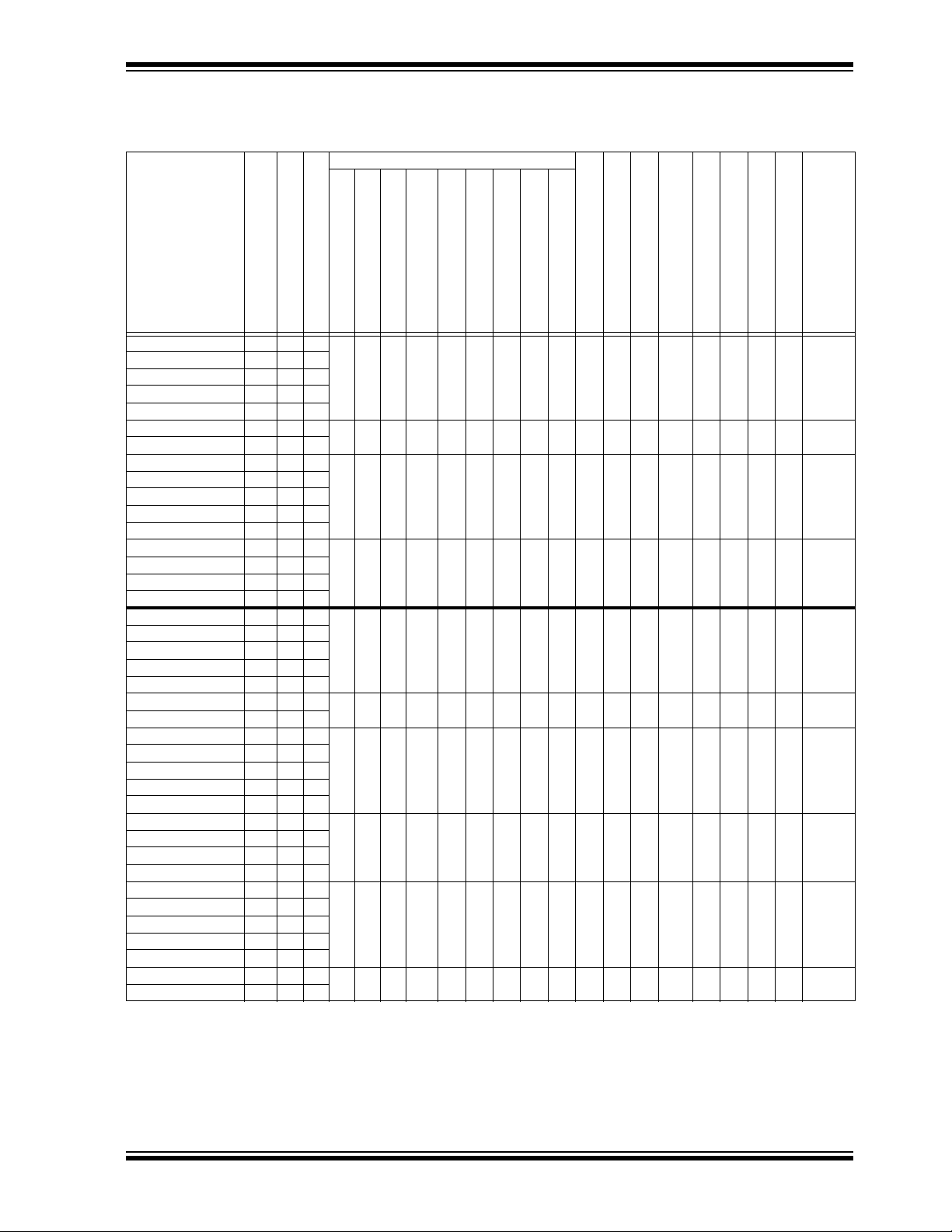
TABLE 1: dsPIC33EPXXXGP50X and PIC24EPXXXGP20X GENERAL PURPOSE FAMILIES
Remappable Peripherals
(3)
Device
RAM (Kbyte)
Page Erase Size (Instructions)
Program Flash Memory (Kbytes)
PIC24EP32GP202 512 32 4
PIC24EP64GP202 1024 64 8
PIC24EP128GP202 1024 128 16
PIC24EP256GP202 1024 256 32
PIC24EP512GP202 1024 512 48
PIC24EP32GP203 512 32 4
PIC24EP64GP203 1024 64 8
PIC24EP32GP204 512 32 4
PIC24EP64GP204 1024 64 8
PIC24EP128GP204 1024 128 16
PIC24EP256GP204 1024 256 32
PIC24EP512GP204 1024 512 48
PIC24EP64GP206 1024 64 8
PIC24EP128GP206 1024 128 16
PIC24EP256GP206 1024 256 32
PIC24EP512GP206 1024 512 48
dsPIC33EP32GP502 512 32 4
dsPIC33EP64GP502 1024 64 8
dsPIC33EP128GP502 1024 128 16
dsPIC33EP256GP502 1024 256 32
dsPIC33EP512GP502 1024 512 48
dsPIC33EP32GP503 512 32 4
dsPIC33EP64GP503 1024 64 8
dsPIC33EP32GP504 512 32 4
dsPIC33EP64GP504 1024 64 8
dsPIC33EP128GP504 1024 128 16
dsPIC33EP256GP504 1024 256 32
dsPIC33EP512GP504 1024 512 48
dsPIC33EP64GP506 1024 64 8
dsPIC33EP128GP506 1024 128 16
dsPIC33EP256GP506 1024 256 32
dsPIC33EP512GP506 1024 512 48
Note 1: On 28-pin devices, Comparator 4 does not have external connections. Refer to Section 25.0 “Op amp/Comparator Module” for details.
2: Only SPI2 is remappable.
3: INT0 is not remappable.
4: The SSOP and VTLA packages are not available for devices with 512 KB of memory.
Input Capture
16-bit/32-bit Timers
54422—32162/3
54422—32183/4YesYes2536VTLA
54422—32193/4YesYes3544
54422—321163/4YesYes5364
54422132162/3
54422132183/4YesYes2536VTLA
54422132193/4YesYes3544
544221321163/4YesYes5364
Output Compare
UART
(2)
SPI
ECAN™ Technology
C™
2
I
CRC Generator
External Interrupts
Op amps/Comparators
10-bit/12-bit ADC (Channels)
(1)
(1)
PTG
CTMU
Yes Yes 21 28
Yes Yes 21 28
I/O Pins
Pins
SPDIP,
SOIC,
SSOP
QFN-S
VTLA
TQFP,
QFN
TQFP,
QFN
SPDIP,
SOIC,
SSOP
QFN-S
VTLA
TQFP,
QFN
TQFP,
QFN
Packages
(4)
(4)
(4)
(4)
,
,
,
,
DS70657E-page 2 Preliminary © 2011-2012 Microchip Technology Inc.
dsPIC33EPXXXGP50X, dsPIC33EPXXXMC20X/50X, AND PIC24EPXXXGP/MC20X
TABLE 2: dsPIC33EPXXXMC20X/50X and PIC24EPXXXMC20X MOTOR CONTROL
FAMILIES
Remappable Peripherals
Device
Page Erase Size (Instructions)
Program Flash Memory (Kbytes)
RAM (Kbytes)
16-bit/32-bit Timers
Input Capture
Output Compare
(4)
Motor Control PWM
(2)
SPI
UART
(Channels)
Quadrature Encoder Interface
ECAN™ Technology
(3)
C™
2
I
CTMU
PTG
I/O Pins
Pins
Packages
CRC Generator
External Interrupts
Op am ps/Co mparators
10-bit/12-bit ADC (Channels)
PIC24EP32MC202 512 32 4
PIC24EP64MC202 1024 64 8
PIC24EP128MC202 1024 128 16
PIC24EP256MC202 1024 256 32
544 6 122—32162/3
(1)
Yes Yes 21 28
SPDIP,
SOIC,
SSOP
QFN-S
(5)
PIC24EP512MC202 1024 512 48
PIC24EP32MC203 512 32 4
PIC24EP64MC203 1024 64 8
5 4 4 6 1 2 2 — 3 2 1 8 3/4 Yes Yes 25 36 VTLA
PIC24EP32MC204 512 32 4
PIC24EP64MC204 1024 64 8
PIC24EP128MC204 1024 128 16
PIC24EP256MC204 1024 256 32
5 4 4 6 1 2 2 — 3 2 1 9 3/4 Yes Yes 35 44
VTLA
TQFP,
QFN
(5)
PIC24EP512MC204 1024 512 48
PIC24EP64MC206 1024 64 8
PIC24EP128MC206 1024 128 16
PIC24EP256MC206 1024 256 32
5 4 4 6 1 2 2 — 3 2 1 16 3/4 Yes Yes 53 64
TQFP,
QFN
PIC24EP512MC206 1024 512 48
dsPIC33EP32MC202 512 32 4
dsPIC33EP64MC202 1024 64 8
dsPIC33EP128MC202 1024 128 16
dsPIC33EP256MC202 1024 256 32
544 6 122—32162/3
(1)
Yes Yes 21 28
SPDIP,
SOIC,
SSOP
QFN-S
(5)
dsPIC33EP512MC202 1024 512 48
dsPIC33EP32MC203 512 32 4
dsPIC33EP64MC203 1024 64 8
5 4 4 6 1 2 2 — 3 2 1 8 3/4 Yes Yes 25 36 VTLA
dsPIC33EP32MC204 512 32 4
dsPIC33EP64MC204 1024 64 8
dsPIC33EP128MC204 1024 128 16
dsPIC33EP256MC204 1024 256 32
5 4 4 6 1 2 2 — 3 2 1 9 3/4 Yes Yes 35 44
VTLA
TQFP,
QFN
(5)
dsPIC33EP512MC204 1024 512 48
dsPIC33EP64MC206 1024 64 8
dsPIC33EP128MC206 1024 128 16
dsPIC33EP256MC206 1024 256 32
5 4 4 6 1 2 2 — 3 2 1 16 3/4 Yes Yes 53 64
TQFP,
QFN
dsPIC33EP512MC206 1024 512 48
dsPIC33EP32MC502 512 32 4
dsPIC33EP64MC502 1024 64 8
dsPIC33EP128MC502 1024 128 16
dsPIC33EP256MC502 1024 256 32
544 6 122132162/3
(1)
Yes Yes 21 28
SPDIP,
SOIC,
SSOP
QFN-S
(5)
dsPIC33EP512MC502 1024 512 48
dsPIC33EP32MC503 512 32 4
dsPIC33EP64MC503 1024 64 8
5 4 4 6 1 2 2 1 3 2 1 8 3/4 Yes Yes 25 36 VTLA
Note 1: On 28-pin devices, Comparator 4 does not have external connections. Refer to Section 25.0 “Op amp/Comparator Module” for details.
2: Only SPI2 is remappable.
3: INT0 is not remappable.
4: Only the PWM Faults are remappable.
5: The SSOP and VTLA packages are not available for devices with 512 KB of memory.
,
,
,
,
,
© 2011-2012 Microchip Technology Inc. Preliminary DS70657E-page 3
dsPIC33EPXXXGP50X, dsPIC33EPXXXMC20X/50X, AND PIC24EPXXXGP/MC20X
TABLE 2: dsPIC33EPXXXMC20X/50X and PIC24EPXXXMC20X MOTOR CONTROL
FAMILIES (CONTINUED)
Remappable Peripherals
(4)
Device
RAM (Kbytes)
Page Erase Size (Instructions)
Program Flash Memory (Kbytes)
dsPIC33EP32MC504 512 32 4
dsPIC33EP64MC504 1024 64 8
dsPIC33EP128MC504 1024 128 16
dsPIC33EP256MC504 1024 256 32
dsPIC33EP512MC504 1024 512 48
dsPIC33EP64MC506 1024 64 8
dsPIC33EP128MC506 1024 128 16
dsPIC33EP256MC506 1024 256 32
dsPIC33EP512MC506 1024 512 48
Note 1: On 28-pin devices, Comparator 4 does not have external connections. Refer to Section 25.0 “Op amp/Comparator Module” for details.
2: Only SPI2 is remappable.
3: INT0 is not remappable.
4: Only the PWM Faults are remappable.
5: The SSOP and VTLA packages are not available for devices with 512 KB of memory.
Input Capture
16-bit/32-bit Timers
5 4 4 6 1 2 2 1 3 2 1 9 3/4 Yes Yes 35 44
5 4 4 6 1 2 2 1 3 2 1 16 3/4 Yes Yes 53 64
(Channels)
Output Compare
Motor Control PWM
Quadrature Encoder Interface
UART
(2)
SPI
ECAN™ Technology
(3)
C™
2
I
CRC Generator
External Interrupts
Op amps/Comparators
10-bit/12-bit ADC (Channels)
CTMU
PTG
I/O Pins
Pins
VTLA
TQFP,
QFN
TQFP,
QFN
Packages
(5)
,
DS70657E-page 4 Preliminary © 2011-2012 Microchip Technology Inc.
dsPIC33EPXXXGP50X, dsPIC33EPXXXMC20X/50X, AND PIC24EPXXXGP/MC20X
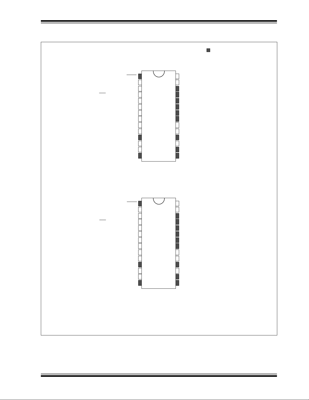
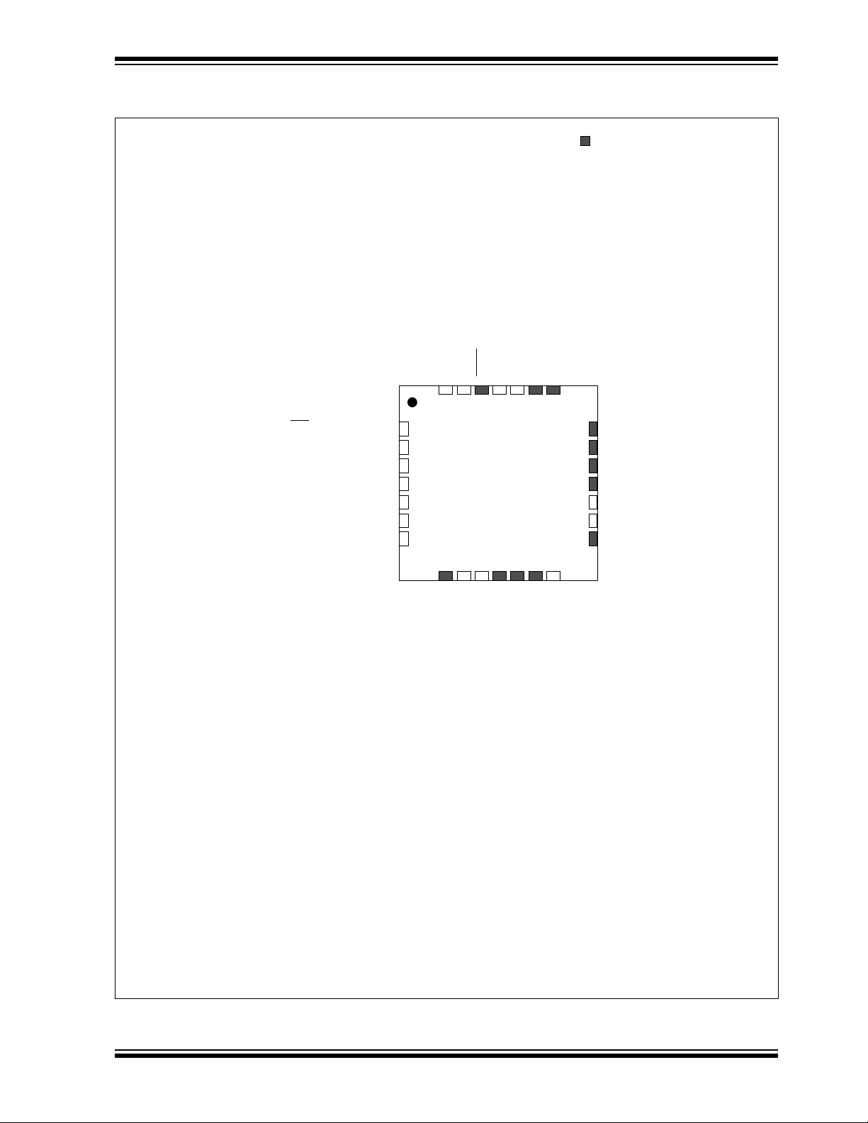
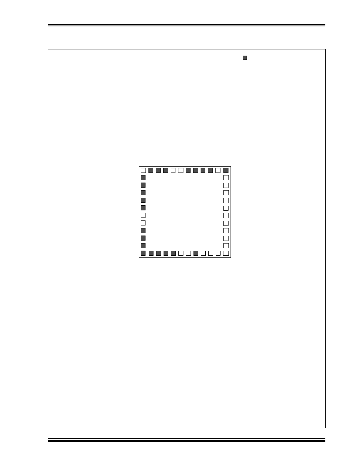
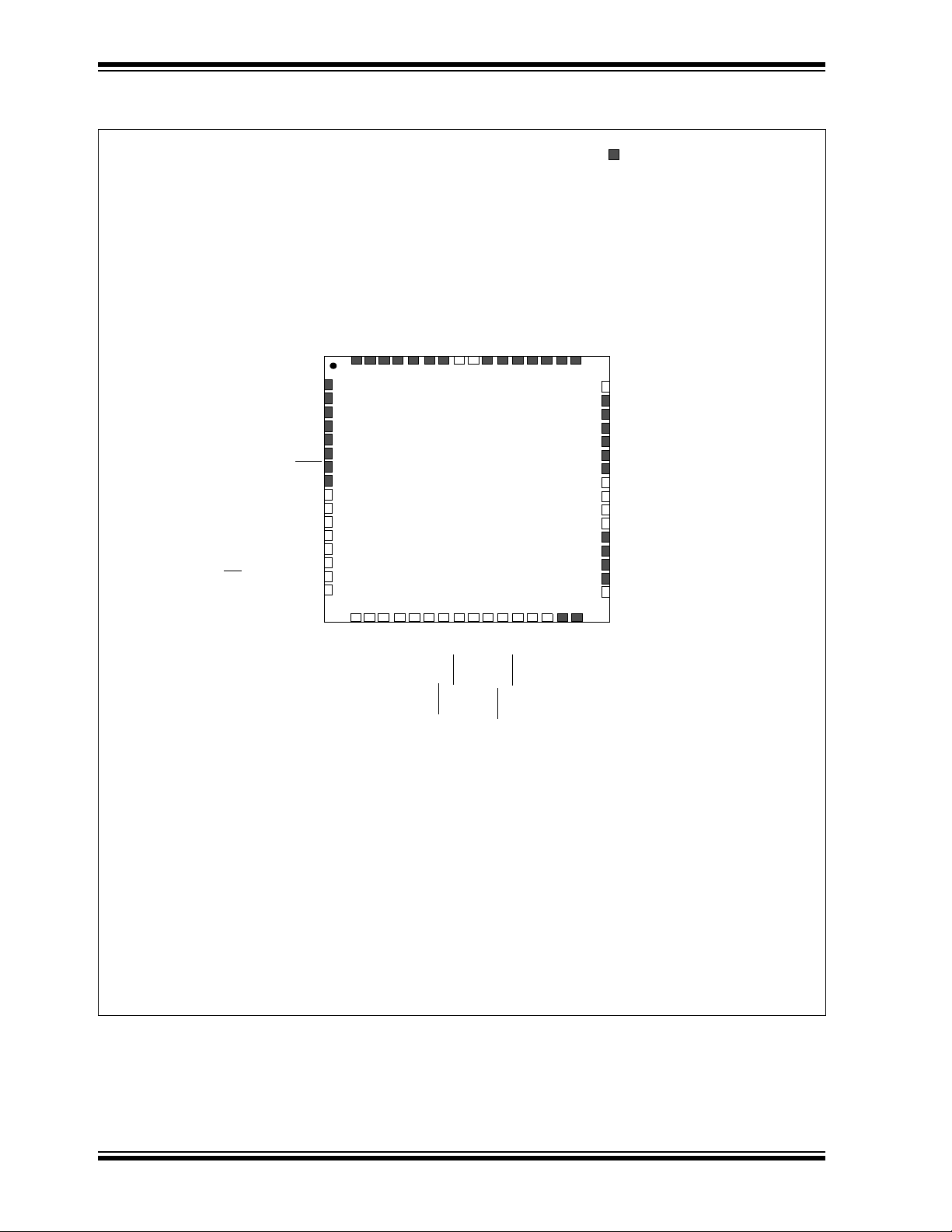
28-Pin SPDIP/SOIC/SSOP
Note 1: The RPn/RPIn pins can be used by any remappable peripheral with some limitation. See Section 11.4
“Peripheral Pin Select” for available peripherals and for information on limitations.
2: Every I/O port pin (RAx-RGx) can be used as change notification (CNAx-CNGx). See Section 11.0
“I/O Ports” for more information.
= Pins are up to 5V tolerant
128
227
326
425
524
623
722
821
920
10 19
11 18
12 17
13 16
14 15
PIC24EPXXXGP202
dsPIC33EPXXXGP502
MCLR AVDD
AN0/OA2OUT/RA0 AVSS
AN1/C2IN1+/RA1 RPI47/T5CK/RB15
PGED3/V
REF-/AN2/C2IN1-/SS1/RPI32/CTED2/RB0 RPI46/T3CK/RB14
PGEC3/V
REF+/AN3/OA1OUT/RPI33/CTED1/RB1 RPI45/CTPLS/RB13
PGEC1/AN4/C1IN1+/RPI34/RB2 RPI44/RB12
PGED1/AN5/C1IN1-/RP35/RB3 TDI/RP43/RB11
TDO/RP42/RB10
OSC1/CLKI/RA2 V
CAP
OSC2/CLKO/RA3 VSS
RP36/RB4 TMS/ASDA1/SDI1/RP41/RB9
CV
REF2O/RP20/T1CK/RA4 TCK/CVREF1O/ASCL1/SDO1/RP40/T4CK/RB8
V
DD SCK1/RP39/INT0/RB7
PGED2/ASDA2/RP37/RB5 PGEC2/ASCL2/RP38/RB6
V
SS
128
227
326
425
524
623
722
821
920
10 19
11 18
12 17
13 16
14 15
PIC24EPXXXMC202
dsPIC33EPXXXMC202/502
MCLR AVDD
AN0/OA2OUT/RA0 AVSS
AN1/C2IN1+/RA1 RPI47/PWM1L/T5CK/RB15
PGED3/V
REF-/AN2/C2IN1-/SS1/RPI32/CTED2/RB0 RPI46/PWM1H/T3CK/RB14
PGEC3/V
REF+/AN3/OA1OUT/RPI33/CTED1/RB1 RPI45/PWM2L/CTPLS/RB13
PGEC1/AN4/C1IN1+/RPI34/RB2 RPI44/PWM2H/RB12
PGED1/AN5/C1IN1-/RP35/RB3 TDI/RP43/PWM3L/RB11
TDO/RP42/PWM3H/RB10
OSC1/CLKI/RA2 V
CAP
OSC2/CLKO/RA3 VSS
FLT32/RP36/RB4 TMS/ASDA1/SDI1/RP41/RB9
CV
REF2O/RP20/T1CK/RA4 TCK/CVREF1O/ASCL1/SDO1/RP40/T4CK/RB8
V
DD SCK1/RP39/INT0/RB7
PGED2/ASDA2/RP37/RB5 PGEC2/ASCL2/RP38/RB6
V
SS
Pin Diagrams
© 2011-2012 Microchip Technology Inc. Preliminary DS70657E-page 5
dsPIC33EPXXXGP50X, dsPIC33EPXXXMC20X/50X, AND PIC24EPXXXGP/MC20X
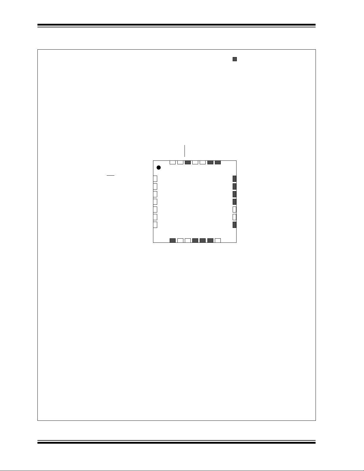
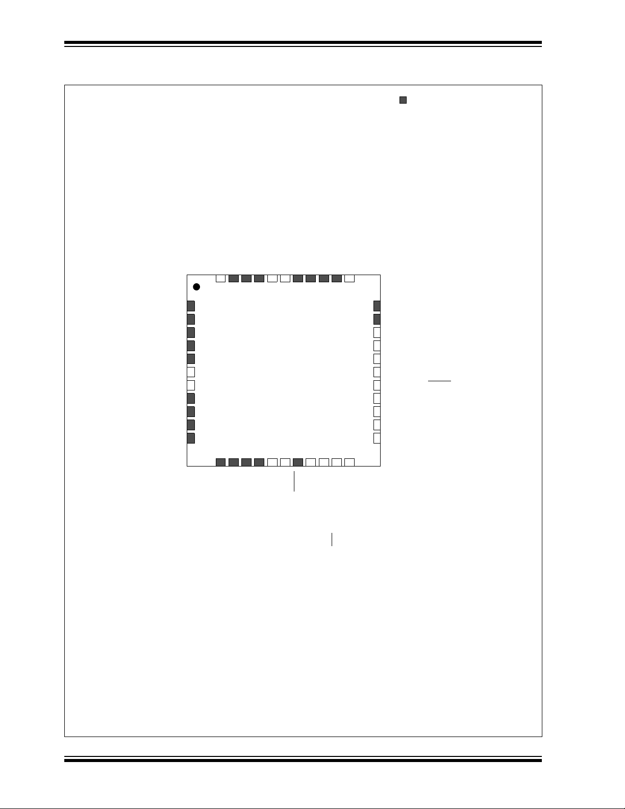
28-Pin QFN-S
(3)
= Pins are up to 5V tolerant
28 27 26 25 24 23 22
8 9 10 11 12 13 14
3
18
17
16
15
4
5
7
1
2 20
19
6
21
PIC24EPXXXGP202
dsPIC33EPXXXGP502
TCK/CVREF1O/ASCL1/SDO1/RP40/T4CK/RB8
SCK1/RP39/INT0/RB7
PGEC2/ASCL2/RP38/RB6
PGED2/ASDA2/RP37/RB5
V
DD
CVREF2O/RP20/T1CK/RA4
RP36/RB4
RPI45/CTPLS/RB13
RPI44/RB12
TDI/RP43/RB11
TDO/RP42/RB10
V
CAP
VSS
TMS/ASDA1/SDI1/RP41/RB9
RPI46/T3CK/RB14
RPI47/T5CK/RB15
AV
SS
AVDD
MCLR
AN0/OA2OUT/RA0
AN1/C2IN1+/RA1
PGED3/VREF-/AN2/C2IN1-/SS1/RPI32/CTED2/RB0
PGEC3/V
REF+/AN3/OA1OUT/RPI33/CTED1/RB1
V
SS
OSC1/CLKI/RA2
OSC2/CLKO/RA3
PGEC1/AN4/C1IN1+/RPI34/RB2
PGED1/AN5/C1IN1-/RP35/RB3
Note 1: The RPn/RPIn pins can be used by any remappable peripheral with some limitation. See Section 11.4
“Peripheral Pin Select” for available peripherals and for information on limitations.
2: Every I/O port pin (RAx-RGx) can be used as change notification (CNAx-CNGx). See Section 11.0
“I/O Ports” for more information.
3: The metal pad at the bottom of the device is not connected to any pins and is recommended to be
connected to V
SS externally.
Pin Diagrams (Continued)
DS70657E-page 6 Preliminary © 2011-2012 Microchip Technology Inc.
dsPIC33EPXXXGP50X, dsPIC33EPXXXMC20X/50X, AND PIC24EPXXXGP/MC20X
28-Pin QFN-S
(3)
= Pins are up to 5V tolerant
28 27 26 25 24 23 22
8 9 10 11 12 13 14
3
18
17
16
15
4
5
7
1
2 20
19
6
21
PIC24EPXXXMC202
dsPIC33EPXXXMC202/502
TCK/CVREF1O/ASCL1/SDO1/RP40/T4CK/RB8
SCK1/RP39/INT0/RB7
PGEC2/ASCL2/RP38/RB6
PGED2/ASDA2/RP37/RB5
V
DD
CVREF2O/RP20/T1CK/RA4
FLT32/RP36/RB4
RPI45/PWM2L/CTPLS/RB13
RPI44/PWM2H/RB12
TDI/RP43/PWM3L/RB11
TDO/RP42/PWM3H/RB10
V
CAP
VSS
TMS/ASDA1/SDI1/RP41/RB9
RPI46/PWM1H/T3CK/RB14
RPI47/PWM1L/T5CK/RB15
AV
SS
AVDD
MCLR
AN0/OA2OUT/RA0
AN1/C2IN1+/RA1
PGED3/VREF-/AN2/C2IN1-/SS1/RPI32/CTED2/RB0
PGEC3/V
REF+/AN3/OA1OUT/RPI33/CTED1/RB1
V
SS
OSC1/CLKI/RA2
OSC2/CLKO/RA3
PGEC1/AN4/C1IN1+/RPI34/RB2
PGED1/AN5/C1IN1-/RP35/RB3
Note 1: The RPn/RPIn pins can be used by any remappable peripheral with some limitation. See Section 11.4
“Peripheral Pin Select” for available peripherals and for information on limitations.
2: Every I/O port pin (RAx-RGx) can be used as change notification (CNAx-CNGx). See Section 11.0
“I/O Ports” for more information.
3: The metal pad at the bottom of the device is not connected to any pins and is recommended to be
connected to V
SS externally.
Pin Diagrams (Continued)
© 2011-2012 Microchip Technology Inc. Preliminary DS70657E-page 7

dsPIC33EPXXXGP50X, dsPIC33EPXXXMC20X/50X, AND PIC24EPXXXGP/MC20X
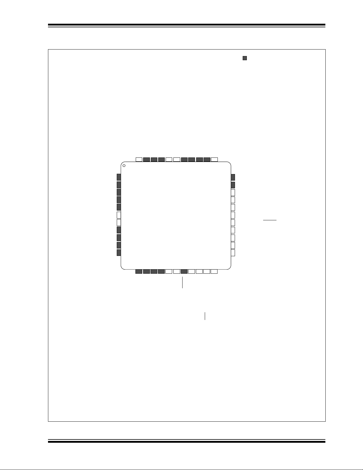
36-Pin VTLA
(3)
1
10
33 32 31 30 29 28
2
3
4
5
6
24
23
22
21
20
19
11 12 13 14 15
7
8
9
34
35
36
16
17
18
27
26
25
= Pins are up to 5V tolerant
PIC24EP32GP203
TCK/CVREF1O/ASCL1/SDO1/RP40/T4CK/RB8
RPI45/CTPLS/RB13
PGEC1/AN4/C1IN1+/RPI34/RB2
PGED1/AN5/C1IN1-/RP35/RB3
AN6/OA3OUT/C4IN1+/OCFB/RC0
AN7/C3IN1-/C4IN1-/RC1
V
DD
VSS
OSC1/CLKI/RA2
OSC2/CLKO/RA3
SDA2/RPI24/RA8
RPI46/T3CK/RB14
RPI47/T5CK/RB15
AV
SS
AVDD
MCLR
AN0/OA2OUT/RA0
AN1/C2IN1+/RA1
PGED3/V
REF-/AN2/C2IN1-/SS1/RPI32/CTED2/RB0
PGEC3/V
REF+/AN3/OA1OUT/RPI33/CTED1/RB1
RPI44/RB12
TDI/RP43/RB11
TDO/RP42/RB10
V
CAP
VSS
RP56/RC8
TMS/ASDA1/SDI1/RP41/RB9
SCK1/RP39/INT0/RB7
PGEC2/ASCL2/RP38/RB6
PGED2/ASDA2/RP37/RB5
V
DD
VSS
CVREF2O/RP20/T1CK/RA4
V
DD
SCL2/RP36/RB4
VDD
Note 1: The RPn/RPIn pins can be used by any remappable peripheral with some limitation. See Section 11.4
“Peripheral Pin Select” for available peripherals and for information on limitations.
2: Every I/O port pin (RAx-RGx) can be used as change notification (CNAx-CNGx). See Section 11.0
“I/O Ports” for more information.
3: The metal pad at the bottom of the device is not connected to any pins and is recommended to be
connected to V
SS externally.
dsPIC33EP32GP503
PIC24EP64GP203
dsPIC33EP64GP503
Pin Diagrams (Continued)
DS70657E-page 8 Preliminary © 2011-2012 Microchip Technology Inc.

dsPIC33EPXXXGP50X, dsPIC33EPXXXMC20X/50X, AND PIC24EPXXXGP/MC20X
36-Pin VTLA
(3)
= Pins are up to 5V tolerant
1
10
33 32 31 30 29 28
2
3
4
5
6
24
23
22
21
20
19
11 12 13 14 15
7
8
9
34
35
36
16
17
18
27
26
25
PIC24EP32MC203
TCK/CVREF1O/ASCL1/SDO1/RP40/T4CK/RB8
RPI45/PWM2L/CTPLS/RB13
PGEC1/AN4/C1IN1+/RPI34/RB2
PGED1/AN5/C1IN1-/RP35/RB3
AN6/OA3OUT/C4IN1+/OCFB/RC0
AN7/C3IN1-/C4IN1-/RC1
V
DD
VSS
OSC1/CLKI/RA2
OSC2/CLKO/RA3
SDA2/RPI24/RA8
RPI46/PWM1H/T3CK/RB14
RPI47/PWM1L/T5CK/RB15
AV
SS
AVDD
MCLR
AN0/OA2OUT/RA0
AN1/C2IN1+/RA1
PGED3/V
REF-/AN2/C2IN1-/SS1/RPI32/CTED2/RB0
PGEC3/V
REF+/AN3/OA1OUT/RPI33/CTED1/RB1
RPI44/PWM2H/RB12
TDI/RP43/PWM3L/RB11
TDO/RP42/PWM3H/RB10
V
CAP
VSS
RP56/RC8
TMS/ASDA1/SDI1/RP41/RB9
SCK1/RP39/INT0/RB7
PGEC2/ASCL2/RP38/RB6
PGED2/ASDA2/RP37/RB5
V
DD
VSS
CVREF2O/RP20/T1CK/RA4
V
DD
FLT32/SCL2/RP36/RB4
VDD
Note 1: The RPn/RPIn pins can be used by any remappable peripheral with some limitation. See Section 11.4
“Peripheral Pin Select” for available peripherals and for information on limitations.
2: Every I/O port pin (RAx-RGx) can be used as change notification (CNAx-CNGx). See Section 11.0
“I/O Ports” for more information.
3: The metal pad at the bottom of the device is not connected to any pins and is recommended to be
connected to V
SS externally.
dsPIC33EP32MC203/503
PIC24EP64MC203
dsPIC33EP64MC203/503
Pin Diagrams (Continued)
© 2011-2012 Microchip Technology Inc. Preliminary DS70657E-page 9
dsPIC33EPXXXGP50X, dsPIC33EPXXXMC20X/50X, AND PIC24EPXXXGP/MC20X
44-Pin TQFP
= Pins are up to 5V tolerant
4443424140393837363534
133
232
331
430
529
628
727
826
925
10 24
11 23
1213141516171819202122
PIC24EPXXXGP204
TCK/CVREF1O/ASCL1/RP40/T4CK/RB8TDO/RA10
RPI45/CTPLS/RB13
PGEC1/AN4/C1IN1+/RPI34/RB2
PGED1/AN5/C1IN1-/RP35/RB3
AN6/OA3OUT/C4IN1+/OCFB/RC0
AN7/C3IN1-/C4IN1-/RC1
AN8/C3IN1+/U1RTS
/BCLK1/RC2
V
DD
VSS
OSC1/CLKI/RA2
OSC2/CLKO/RA3
SDA2/RPI24/RA8
SCL2/RP36/RB4
TDI/RA7
RPI46/T3CK/RB14
RPI47/T5CK/RB15
AV
SS
AVDD
MCLR
AN0/OA2OUT/RA0
AN1/C2IN1+/RA1
PGED3/V
REF-/AN2/C2IN1-/SS1/RPI32/CTED2/RB0
PGEC3/V
REF+/AN3/OA1OUT/RPI33/CTED1/RB1
RPI44/RB12
RP43/RB11
RP42/RB10
V
CAP
VSS
RP57/RC9
RP56/RC8
RP55/RC7
RP54/RC6
TMS/ASDA1/RP41/RB9
RP39/INT0/RB7
PGEC2/ASCL2/RP38/RB6
PGED2/ASDA2/RP37/RB5
VDDVSS
SCL1/RPI53/RC5
SDA1/RPI52/RC4
SCK1/RPI51/RC3
SDI1/RPI25/RA9
CV
REF2O/SDO1/RP20/T1CK/RA4
Note 1: The RPn/RPIn pins can be used by any remappable peripheral with some limitation. See Section 11.4
“Peripheral Pin Select” for available peripherals and for information on limitations.
2: Every I/O port pin (RAx-RGx) can be used as change notification (CNAx-CNGx). See Section 11.0
“I/O Ports” for more information.
dsPIC33EPXXXGP504
Pin Diagrams (Continued)
DS70657E-page 10 Preliminary © 2011-2012 Microchip Technology Inc.
dsPIC33EPXXXGP50X, dsPIC33EPXXXMC20X/50X, AND PIC24EPXXXGP/MC20X
44-Pin TQFP
= Pins are up to 5V tolerant
4443424140393837363534
133
232
331
430
529
628
727
826
925
10 24
11 23
1213141516171819202122
PIC24EPXXXMC204
TCK/CVREF1O/ASCL1/RP40/T4CK/RB8TDO/RA10
RPI45/PWM2L/CTPLS/RB13
PGEC1/AN4/C1IN1+/RPI34/RB2
PGED1/AN5/C1IN1-/RP35/RB3
AN6/OA3OUT/C4IN1+/OCFB/RC0
AN7/C3IN1-/C4IN1-/RC1
AN8/C3IN1+/U1RTS
/BCLK1/FLT3/RC2
V
DD
VSS
OSC1/CLKI/RA2
OSC2/CLKO/RA3
SDA2/RPI24/RA8
FLT32/SCL2/RP36/RB4
TDI/RA7
RPI46/PWM1H/T3CK/RB14
RPI47/PWM1L/T5CK/RB15
AV
SS
AVDD
MCLR
AN0/OA2OUT/RA0
AN1/C2IN1+/RA1
PGED3/V
REF-/AN2/C2IN1-/SS1/RPI32/CTED2/RB0
PGEC3/V
REF+/AN3/OA1OUT/RPI33/CTED1/RB1
RPI44/PWM2H/RB12
RP43/PWM3L/RB11
RP42/PWM3H/RB10
V
CAP
VSS
RP57/RC9
RP56/RC8
RP55/RC7
RP54/RC6
TMS/ASDA1/RP41/RB9
RP39/INT0/RB7
PGEC2/ASCL2/RP38/RB6
PGED2/ASDA2/RP37/RB5
VDDVSS
SCL1/RPI53/RC5
SDA1/RPI52/RC4
SCK1/RPI51/RC3
SDI1/RPI25/RA9
CV
REF2O/SDO1/RP20/T1CK/RA4
Note 1: The RPn/RPIn pins can be used by any remappable peripheral with some limitation. See Section 11.4
“Peripheral Pin Select” for available peripherals and for information on limitations.
2: Every I/O port pin (RAx-RGx) can be used as change notification (CNAx-CNGx). See Section 11.0
“I/O Ports” for more information.
dsPIC33EPXXXMC204/504
Pin Diagrams (Continued)
© 2011-2012 Microchip Technology Inc. Preliminary DS70657E-page 11
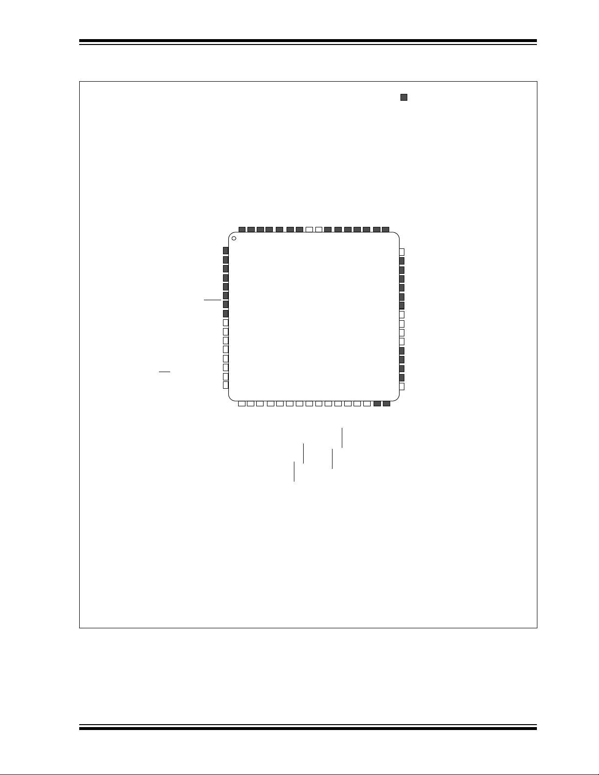
dsPIC33EPXXXGP50X, dsPIC33EPXXXMC20X/50X, AND PIC24EPXXXGP/MC20X
44-Pin VTLA
(3)
= Pins are up to 5V tolerant
PIC24EPXXXGP204
1
12
41 40 39 38 37 36 35 34
2
3
4
5
6
7
8
30
29
28
27
26
25
24
23
13 14 15 16 17 18 19
9
10
11
2220
21
33
32
31
424344
PGEC1/AN4/C1IN1+/RPI34/RB2
PGED1/AN5/C1IN1-/RP35/RB3
AN6/OA3OUT/C4IN1+/OCFB/RC0
AN7/C3IN1-/C4IN1-/RC1
AN8/C3IN1+/U1RTS
/BCLK1/RC2
V
DD
VSS
OSC1/CLKI/RA2
OSC2/CLKO/RA3
SDA2/RPI24/RA8
SCL2/RP36/RB4
TCK/CVREF1O/ASCL1/RP40/T4CK/RB8
RP39/INT0/RB7
PGEC2/ASCL2/RP38/RB6
PGED2/ASDA2/RP37/RB5
V
DD
VSS
SCL1/RPI53/RC5
SDA1/RPI52/RC4
SCK1/RPI51/RC3
SDI1/RPI25/RA9
CVREF2O/SDO1/RP20/T1CK/RA4
RPI45/CTPLS/RB13
RPI44/RB12
RP43/RB11
RP42/RB10
V
CAP
VSS
RP57/RC9
RP56/RC8
RP55/RC7
RP54/RC6
TMS/ASDA1/RP41/RB9
TDO/RA10
TDI/RA7
RPI46/T3CK/RB14
RPI47/T5CK/RB15
AV
SS
AVDD
MCLR
AN0/OA2OUT/RA0
AN1/C2IN1+/RA1
PGED3/V
REF-/AN2/C2IN1-/SS1/RPI32/CTED2/RB0
PGEC3/V
REF+/AN3/OA1OUT/RPI33/CTED1/RB1
Note 1: The RPn/RPIn pins can be used by any remappable peripheral with some limitation. See Section 11.4
“Peripheral Pin Select” for available peripherals and for information on limitations.
2: Every I/O port pin (RAx-RGx) can be used as change notification (CNAx-CNGx). See Section 11.0
“I/O Ports” for more information.
3: The metal pad at the bottom of the device is not connected to any pins and is recommended to be
connected to V
SS externally.
dsPIC33EPXXXGP504
Pin Diagrams (Continued)
DS70657E-page 12 Preliminary © 2011-2012 Microchip Technology Inc.
dsPIC33EPXXXGP50X, dsPIC33EPXXXMC20X/50X, AND PIC24EPXXXGP/MC20X
44-Pin VTLA
(3)
= Pins are up to 5V tolerant
PIC24EPXXXMC204
1
12
41 40 39 38 37 36 35 34
2
3
4
5
6
7
8
30
29
28
27
26
25
24
23
13 14 15 16 17 18 19
9
10
11
22
20
21
33
32
31
424344
PGEC1/AN4/C1IN1+/RPI34/RB2
PGED1/AN5/C1IN1-/RP35/RB3
AN6/OA3OUT/C4IN1+/OCFB/RC0
AN7/C3IN1-/C4IN1-/RC1
AN8/C3IN1+/U1RTS
/BCLK1/FLT3/RC2
V
DD
VSS
OSC1/CLKI/RA2
OSC2/CLKO/RA3
SDA2/RPI24/RA8
FLT32/SCL2/RP36/RB4
TCK/CVREF1O/ASCL1/RP40/T4CK/RB8
RP39/INT0/RB7
PGEC2/ASCL2/RP38/RB6
PGED2/ASDA2/RP37/RB5
V
DD
VSS
SCL1/RPI53/RC5
SDA1/RPI52/RC4
SCK1/RPI51/RC3
SDI1/RPI25/RA9
CV
REF2O/SDO1/RP20/T1CK/RA4
RPI45/PWM2L/CTPLS/RB13
RPI44/PWM2H/RB12
RP43/PWM3L/RB11
RP42/PWM3H/RB10
V
CAP
VSS
RP57/RC9
RP56/RC8
RP55/RC7
RP54/RC6
TMS/ASDA1/RP41/RB9
TDO/RA10
TDI/RA7
RPI46/PWM1H/T3CK/RB14
RPI47/PWM1L/T5CK/RB15
AV
SS
AVDD
MCLR
AN0/OA2OUT/RA0
AN1/C2IN1+/RA1
PGED3/V
REF-/AN2/C2IN1-/SS1/RPI32/CTED2/RB0
PGEC3/V
REF+/AN3/OA1OUT/RPI33/CTED1/RB1
Note 1: The RPn/RPIn pins can be used by any remappable peripheral with some limitation. See Section 11.4
“Peripheral Pin Select” for available peripherals and for information on limitations.
2: Every I/O port pin (RAx-RGx) can be used as change notification (CNAx-CNGx). See Section 11.0
“I/O Ports” for more information.
3: The metal pad at the bottom of the device is not connected to any pins and is recommended to be
connected to V
SS externally.
dsPIC33EPXXXMC204/504
Pin Diagrams (Continued)
© 2011-2012 Microchip Technology Inc. Preliminary DS70657E-page 13
dsPIC33EPXXXGP50X, dsPIC33EPXXXMC20X/50X, AND PIC24EPXXXGP/MC20X
44-Pin QFN
(3)
= Pins are up to 5V tolerant
44 43 42 41 40 39 38 37 36 35
12 13 14 15 16 17 18 19 20 21
3
30
29
28
27
26
25
24
23
4
5
7
8
9
10
11
1
2 32
31
6
22
33
34
PIC24EPXXXGP204
PGEC1/AN4/C1IN1+/RPI34/RB2
PGED1/AN5/C1IN1-/RP35/RB3
AN6/OA3OUT/C4IN1+/OCFB/RC0
AN7/C3IN1-/C4IN1-/RC1
AN8/C3IN1+/U1RTS
/BCLK1/RC2
V
DD
VSS
OSC1/CLKI/RA2
OSC2/CLKO/RA3
SDA2/RPI24/RA8
SCL2/RP36/RB4
TCK/CVREF1O/ASCL1/RP40/T4CK/RB8
RP39/INT0/RB7
PGEC2/ASCL2/RP38/RB6
PGED2/ASDA2/RP37/RB5
VDD
VSS
SCL1/RPI53/RC5
SDA1/RPI52/RC4
SCK1/RPI51/RC3
SDI1/RPI25/RA9
CV
REF2O/SDO1/RP20/T1CK/RA4
RPI45/CTPLS/RB13
RPI44/RB12
RP43/RB11
RP42/RB10
V
CAP
VSS
RP57/RC9
RP56/RC8
RP55/RC7
RP54/RC6
TMS/ASDA1/RP41/RB9
TDO/RA10
TDI/RA7
RPI46/T3CK/RB14
RPI47/T5CK/RB15
AV
SS
AVDD
MCLR
AN0/OA2OUT/RA0
AN1/C2IN1+/RA1
PGED3/V
REF-/AN2/C2IN1-/SS1/RPI32/CTED2/RB0
PGEC3/V
REF+/AN3/OA1OUT/RPI33/CTED1/RB1
Note 1: The RPn/RPIn pins can be used by any remappable peripheral with some limitation. See Section 11.4
“Peripheral Pin Select” for available peripherals and for information on limitations.
2: Every I/O port pin (RAx-RGx) can be used as change notification (CNAx-CNGx). See Section 11.0
“I/O Ports” for more information.
3: The metal pad at the bottom of the device is not connected to any pins and is recommended to be
connected to V
SS externally.
dsPIC33EPXXXGP504
Pin Diagrams (Continued)
DS70657E-page 14 Preliminary © 2011-2012 Microchip Technology Inc.

dsPIC33EPXXXGP50X, dsPIC33EPXXXMC20X/50X, AND PIC24EPXXXGP/MC20X
44-Pin QFN
(3)
= Pins are up to 5V tolerant
44 43 42 41 40 39 38 37 36 35
12 13 14 15 16 17 18 19 20 21
3
30
29
28
27
26
25
24
23
4
5
7
8
9
10
11
1
2 32
31
6
22
33
34
PIC24EPXXXMC204
PGEC1/AN4/C1IN1+/RPI34/RB2
PGED1/AN5/C1IN1-/RP35/RB3
AN6/OA3OUT/C4IN1+/OCFB/RC0
AN7/C3IN1-/C4IN1-/RC1
AN8/C3IN1+/U1RTS
/BCLK1/FLT3/RC2
V
DD
VSS
OSC1/CLKI/RA2
OSC2/CLKO/RA3
SDA2/RPI24/RA8
FLT32/SCL2/RP36/RB4
TCK/CVREF1O/ASCL1/RP40/T4CK/RB8
RP39/INT0/RB7
PGEC2/ASCL2/RP38/RB6
PGED2/ASDA2/RP37/RB5
VDD
VSS
SCL1/RPI53/RC5
SDA1/RPI52/RC4
SCK1/RPI51/RC3
SDI1/RPI25/RA9
CV
REF2O/SDO1/RP20/T1CK/RA4
RPI45/PWM2L/CTPLS/RB13
RPI44/PWM2H/RB12
RP43/PWM3L/RB11
RP42/PWM3H/RB10
V
CAP
VSS
RP57/RC9
RP56/RC8
RP55/RC7
RP54/RC6
TMS/ASDA1/RP41/RB9
TDO/RA10
TDI/RA7
RPI46/PWM1H/T3CK/RB14
RPI47/PWM1L/T5CK/RB15
AV
SS
AVDD
MCLR
AN0/OA2OUT/RA0
AN1/C2IN1+/RA1
PGED3/V
REF-/AN2/C2IN1-/SS1/RPI32/CTED2/RB0
PGEC3/V
REF+/AN3/OA1OUT/RPI33/CTED1/RB1
Note 1: The RPn/RPIn pins can be used by any remappable peripheral with some limitation. See Section 11.4
“Peripheral Pin Select” for available peripherals and for information on limitations.
2: Every I/O port pin (RAx-RGx) can be used as change notification (CNAx-CNGx). See Section 11.0
“I/O Ports” for more information.
3: The metal pad at the bottom of the device is not connected to any pins and is recommended to be
connected to V
SS externally.
dsPIC33EPXXXMC204/504
Pin Diagrams (Continued)
© 2011-2012 Microchip Technology Inc. Preliminary DS70657E-page 15
dsPIC33EPXXXGP50X, dsPIC33EPXXXMC20X/50X, AND PIC24EPXXXGP/MC20X
64-Pin TQFP
= Pins are up to 5V tolerant
646362616059585756555453525150
49
148
247
346
445
544
643
742
841
940
10 39
11 38
12 37
13 36
14 35
15 34
16 33
171819202122232425262728293031
32
TDI/RA7
RPI46/T3CK/RB14
RPI47/T5CK/RB15
RP118/RG6
RPI119/RG7
RP120/RG8
MCLR
RPI121/RG9
V
SS
V
DD
AN10/RPI28/RA12
AN9/RPI27/RA11
AN0/OA2OUT/RA0
AN1/C2IN1+/RA1
PGED3/V
REF
-/AN2/C2IN1-/SS1/RPI32/CTED2/RB0
PGEC3/V
REF
+/AN3/OA1OUT/RPI33/CTED1/RB1
TDO/RA10
RPI45/CTPLS/RB13
RPI44/RB12
RP43/RB11
RP42/RB10
RP97/RF1
RPI96/RF0
VDDV
CAP
RP57/RC9
RD6
RD5
RP56/RC8
RP55/RC7
RP54/RC6
TMS/ASDA1/RP41/RB9
TCK/CV
REF1O
/ASCL1/RP40/T4CK/RB8
RC13
RP39/INT0/RB7
RPI58/RC10
PGEC2/ASCL2/RP38/RB6
PGED2/ASDA2/RP37/RB5
RD8
V
SS
OSC2/CLKO/RC15
OSC1/CLKI/RC12
V
DD
SCL1/RPI53/RC5
SDA1/RPI52/RC4
SCK1/RPI51/RC3
SDI1/RPI25/RA9
CV
REF2O
/SDO1/RP20/T1CK/RA4
PGEC1/AN4/C1IN1+/RPI34/RB2
PGED1/AN5/C1IN1-/RP35/RB3
AV
DD
AV
SS
AN6/OA3OUT/C4IN1+/OCFB/RC0
AN7/C3IN1-/C4IN1-/RC1
AN8/C3IN1+/U1RTS
/BCLK1/RC2
AN11/C1IN2-
(3)
/U1CTS/RC11
V
SS
V
DD
AN12/C2IN2-
(3)
/U2RTS/BCLK2/RE12
AN13/C3IN2-
(3)
/U2CTS/RE13
AN14/RPI94/RE14
AN15/RPI95/RE15
SDA2/RPI24/RA8
SCL2/RP36/RB4
Note 1: The RPn/RPIn pins can be used by any remappable peripheral with some limitation. See Section 11.4
“Peripheral Pin Select” for available peripherals and for information on limitations.
2: Every I/O port pin (RAx-RGx) can be used as change notification (CNAx-CNGx). See Section 11.0 “I/
O Ports” for more information.
3: This pin is not available as an input when OPMODE (CMxCON<10>) = 1.
dsPIC33EP64GP506
PIC24EP64GP206
PIC24EP128GP206
PIC24EP256GP206
dsPIC33EP128GP506
dsPIC33EP256GP506
dsPIC33EP512GP506
PIC24EP512GP206
Pin Diagrams (Continued)
DS70657E-page 16 Preliminary © 2011-2012 Microchip Technology Inc.
dsPIC33EPXXXGP50X, dsPIC33EPXXXMC20X/50X, AND PIC24EPXXXGP/MC20X
64-Pin TQFP
= Pins are up to 5V tolerant
646362616059585756555453525150
49
148
247
346
445
544
643
742
841
940
10 39
11 38
12 37
13 36
14 35
15 34
16 33
171819202122232425262728293031
32
TDI/RA7
RPI46/PWM1H/T3CK/RB14
RPI47/PWM1L/T5CK/RB15
RP118/RG6
RPI119/RG7
RP120/RG8
MCLR
RPI121/RG9
V
SS
V
DD
AN10/RPI28/RA12
AN9/RPI27/RA11
AN0/OA2OUT/RA0
AN1/C2IN1+/RA1
PGED3/
V
REF
-/AN2/C2IN1-/SS1/RPI32/CTED2/RB0
PGEC3/
V
REF
+/AN3/OA1OUT/RPI33/CTED1/RB1
TDO/RA10
RPI45/PWM2L/CTPLS/RB13
RPI44/PWM2H/RB12
RP43/PWM3L/RB11
RP42/PWM3H/RB10
RP97/RF1
RPI96/RF0
VDDV
CAP
RP57/RC9
RD6
RD5
RP56/RC8
RP55/RC7
RP54/RC6
TMS/ASDA1/RP41/RB9
TCK/
CV
REF1O
/ASCL1/RP40/T4CK/RB8
RC13
RP39/INT0/RB7
RPI58/RC10
PGEC2/ASCL2/RP38/RB6
PGED2/ASDA2/RP37/RB5
RD8
V
SS
OSC2/CLKO/RC15
OSC1/CLKI/RC12
V
DD
SCL1/RPI53/RC5
SDA1/RPI52/RC4
SCK1/RPI51/RC3
SDI1/RPI25/RA9
CV
REF2O
/SDO1/RP20/T1CK/RA4
PGEC1/AN4/C1IN1+/RPI34/RB2
PGED1/AN5/C1IN1-/RP35/RB3
AV
DD
AV
SS
AN6/OA3OUT/C4IN1+/OCFB/RC0
AN7/C3IN1-/C4IN1-/RC1
AN8/C3IN1+/U1RTS
/
BCLK1/
FLT3/RC2
AN11/C1IN2-
(3)
/U1CTS/F LT4/ RC 11
V
SS
V
DD
AN12/C2IN2-
(3)
/U2RTS/
BCLK2/
RE12
AN13/C3IN2-
(3)
/U2CTS/RE13
AN14/RPI94/RE14
AN15/RPI95/RE15
SDA2/RPI24/RA8
FLT32
/SCL2/RP36/RB4
Note 1: The RPn/RPIn pins can be used by any remappable peripheral with some limitation. See Section 11.4
“Peripheral Pin Select” for available peripherals and for information on limitations.
2: Every I/O port pin (RAx-RGx) can be used as change notification (CNAx-CNGx). See Section 11.0 “I/
O Ports” for more information.
3: This pin is not available as an input when OPMODE (CMxCON<10>) = 1.
PIC24EP64MC206
dsPIC33EP64MC206/506
PIC24EP128MC206
PIC24EP256MC206
dsPIC33EP128MC206/506
dsPIC33EP256MC206/506
dsPIC33EP512MC206/506
PIC24EP512MC206
Pin Diagrams (Continued)
© 2011-2012 Microchip Technology Inc. Preliminary DS70657E-page 17
dsPIC33EPXXXGP50X, dsPIC33EPXXXMC20X/50X, AND PIC24EPXXXGP/MC20X
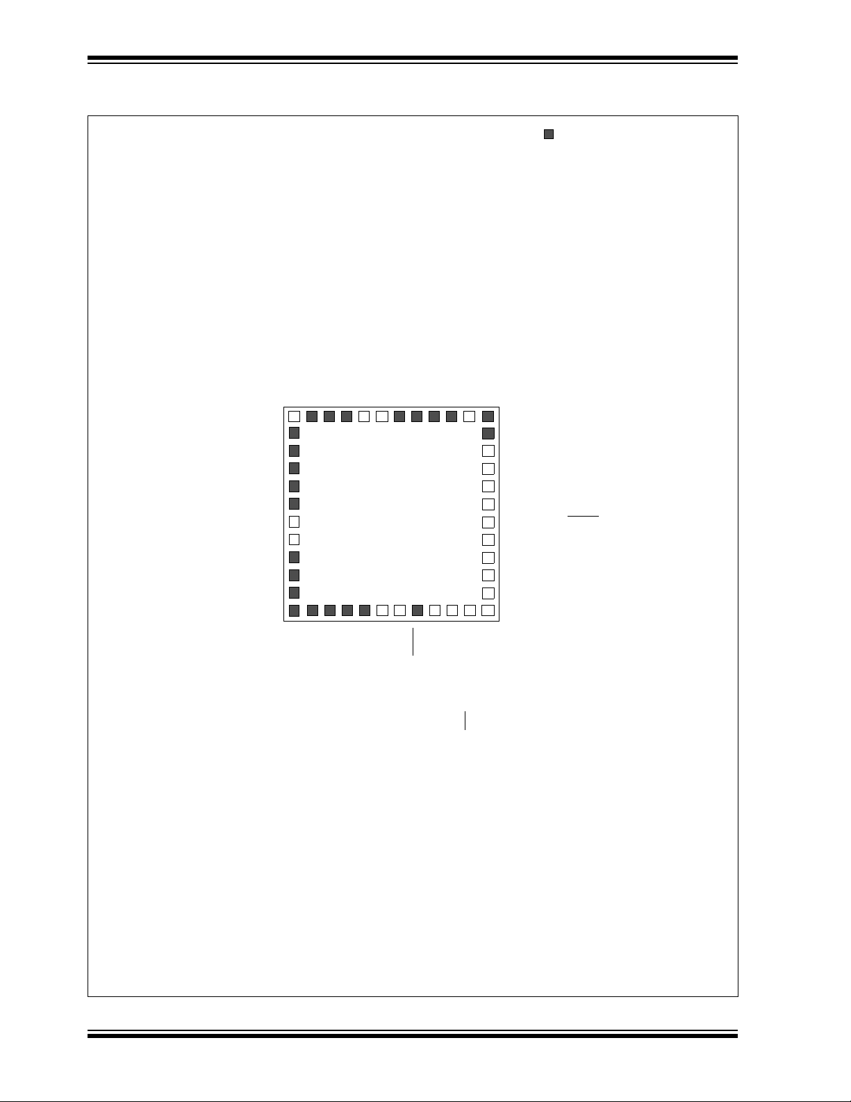
64-Pin QFN
(4)
= Pins are up to 5V tolerant
TDO/RA10
RPI45/CTPLS/RB13
RPI44/RB12
RP43/RB11
RP42/RB10
RP97/RF1
RPI96/RF0
VDDV
CAP
RP57/RC9
RD6
RD5
RP56/RC8
RP55/RC7
RP54/RC6
TMS/ASDA1/RP41/RB9
TCK/
CV
REF1O
/ASCL1/RP40/T4CK/RB8
RC13
RP39/INT0/RB7
RPI58/RC10
PGEC2/ASCL2/RP38/RB6
PGED2/ASDA2/RP37/RB5
RD8
V
SS
OSC2/CLKO/RC15
OSC1/CLKI/RC12
V
DD
SCL1/RPI53/RC5
SDA1/RPI52/RC4
SCK1/RPI51/RC3
SDI1/RPI25/RA9
CV
REF2O
/SDO1/RP20/T1CK/RA4
PGEC1/AN4/C1IN1+/RPI34/RB2
PGED1/AN5/C1IN1-/RP35/RB3
AV
DD
AV
SS
AN6/OA3OUT/C4IN1+/OCFB/RC0
AN7/C3IN1-/C4IN1-/RC1
AN8/C3IN1+/U1RTS/
BCLK1/
RC2
AN11/C1IN2-
(3)
/U1CTS/RC11
V
SS
V
DD
AN12/C2IN2-
(3)
/U2RTS/
BCLK2/
RE12
AN13/C3IN2-
(3)
/U2CTS/RE13
AN14/RPI94/RE14
AN15/RPI95/RE15
SDA2/RPI24/RA8
SCL2/RP36/RB4
TDI/RA7
RPI46/T3CK/RB14
RPI47/T5CK/RB15
RP118/RG6
RPI119/RG7
RP120/RG8
MCLR
RPI121/RG9
V
SS
V
DD
AN10/RPI28/RA12
AN9/RPI27/RA11
AN0/OA2OUT/RA0
AN1/C2IN1+/RA1
PGED3/
V
REF
-/AN2/C2IN1-/SS1/RPI32/CTED2/RB0
PGEC3/
V
REF
+/AN3/OA1OUT/RPI33/CTED1/RB1
PIC24EP64GP206
646362616059585756555453525150
49
148
247
346
445
544
643
742
841
940
10 39
11 38
12 37
13 36
14 35
15 34
16 33
171819202122232425262728293031
32
Note 1: The RPn/RPIn pins can be used by any remappable peripheral with some limitation. See Section 11.4
“Peripheral Pin Select” for available peripherals and for information on limitations.
2: Every I/O port pin (RAx-RGx) can be used as change notification (CNAx-CNGx). See Section 11.0 “I/
O Ports” for more information.
3: This pin is not available as an input when OPMODE (CMxCON<10>) = 1.
4: The metal pad at the bottom of the device is not connected to any pins and is recommended to be
connected to V
SS externally.
dsPIC33EP64GP506
PIC24EP128GP206
PIC24EP256GP206
dsPIC33EP128GP506
dsPIC33EP256GP506
dsPIC33EP512GP506
PIC24EP512GP206
Pin Diagrams (Continued)
DS70657E-page 18 Preliminary © 2011-2012 Microchip Technology Inc.
dsPIC33EPXXXGP50X, dsPIC33EPXXXMC20X/50X, AND PIC24EPXXXGP/MC20X
64-Pin QFN
(4)
= Pins are up to 5V tolerant
646362616059585756555453525150
49
148
247
346
445
544
643
742
841
940
10 39
11 38
12 37
13 36
14 35
15 34
16 33
171819202122232425262728293031
32
TDO/RA10
RPI45/PWM2L/CTPLS/RB13
RPI44/PWM2H/RB12
RP43/PWM3L/RB11
RP42/PWM3H/RB10
RP97/RF1
RPI96/RF0
VDDV
CAP
RP57/RC9
RD6
RD5
RP56/RC8
RP55/RC7
RP54/RC6
TMS/ASDA1/RP41/RB9
TCK/
CV
REF1O
/ASCL1/RP40/T4CK/RB8
RC13
RP39/INT0/RB7
RPI58/RC10
PGEC2/ASCL2/RP38/RB6
PGED2/ASDA2/RP37/RB5
RD8
V
SS
OSC2/CLKO/RC15
OSC1/CLKI/RC12
V
DD
SCL1/RPI53/RC5
SDA1/RPI52/RC4
SCK1/RPI51/RC3
SDI1/RPI25/RA9
CV
REF2O
/SDO1/RP20/T1CK/RA4
PGEC1/AN4/C1IN1+/RPI34/RB2
PGED1/AN5/C1IN1-/RP35/RB3
AV
DD
AV
SS
AN6/OA3OUT/C4IN1+/OCFB/RC0
AN7/C3IN1-/C4IN1-/RC1
AN8/C3IN1+/U1RTS/
BCLK1/
FLT3/RC2
AN11/C1IN2-
(3)
/U1CTS/F LT4 /RC 11
V
SS
V
DD
AN12/C2IN2-
(3)
/U2RTS/
BCLK2/
RE12
AN13/C3IN2-
(3)
/U2CTS/RE13
AN14/RPI94/RE14
AN15/RPI95/RE15
SDA2/RPI24/RA8
FLT32
/SCL2/RP36/RB4
TDI/RA7
RPI46/PWM1H/T3CK/RB14
RPI47/PWM1L/T5CK/RB15
RP118/RG6
RPI119/RG7
RP120/RG8
MCLR
RPI121/RG9
V
SS
V
DD
AN10/RPI28/RA12
AN9/RPI27/RA11
AN0/OA2OUT/RA0
AN1/C2IN1+/RA1
PGED3/
V
REF
-/AN2/C2IN1-/SS1/RPI32/CTED2/RB0
PGEC3/
V
REF
+/AN3/OA1OUT/RPI33/CTED1/RB1
Note 1: The RPn/RPIn pins can be used by any remappable peripheral with some limitation. See Section 11.4
“Peripheral Pin Select” for available peripherals and for information on limitations.
2: Every I/O port pin (RAx-RGx) can be used as change notification (CNAx-CNGx). See Section 11.0 “I/O
Ports” for more information.
3: This pin is not available as an input when OPMODE (CMxCON<10>) = 1.
4: The metal pad at the bottom of the device is not connected to any pins and is recommended to be
connected to V
SS externally.
PIC24EP64MC206
dsPIC33EP64MC206/506
PIC24EP128MC206
PIC24EP256MC206
dsPIC33EP128MC206/506
dsPIC33EP256MC206/506
dsPIC33EP512MC206/506
PIC24EP512MC206
Pin Diagrams (Continued)
© 2011-2012 Microchip Technology Inc. Preliminary DS70657E-page 19

dsPIC33EPXXXGP50X, dsPIC33EPXXXMC20X/50X, AND PIC24EPXXXGP/MC20X
Table of Contents
1.0 Device Overview ........................................................................................................................................................................ 23
2.0 Guidelines for Getting Started with 16-bit Digital Signal Controllers and Microcontrollers......................................................... 27
3.0 CPU............................................................................................................................................................................................ 33
4.0 Memory Organization................................................................................................................................................................. 43
5.0 Flash Program Memory............................................................................................................................................................ 117
6.0 Resets ..................................................................................................................................................................................... 121
7.0 Interrupt Controller ................................................................................................................................................................... 125
8.0 Direct Memory Access (DMA).................................................................................................................................................. 137
9.0 Oscillator Configuration............................................................................................................................................................ 151
10.0 Power-Saving Features............................................................................................................................................................ 161
11.0 I/O Ports ................................................................................................................................................................................... 171
12.0 Timer1 ...................................................................................................................................................................................... 203
13.0 Timer2/3 and Timer4/5 ............................................................................................................................................................ 207
14.0 Input Capture............................................................................................................................................................................ 213
15.0 Output Compare....................................................................................................................................................................... 219
16.0 High-Speed PWM Module (dsPIC33EPXXXMC20X/50X and PIC24EPXXXMC20X Devices Only) ....................................... 225
17.0 Quadrature Encoder Interface (QEI) Module (dsPIC33EPXXXMC20X/50X and PIC24EPXXXMC20X Devices Only)........... 249
18.0 Serial Peripheral Interface (SPI)............................................................................................................................................... 265
19.0 Inter-Integrated Circuit™ (I
20.0 Universal Asynchronous Receiver Transmitter (UART) ........................................................................................................... 281
21.0 Enhanced CAN (ECAN™) Module (dsPIC33EPXXXGP/MC50X Devices Only) ..................................................................... 287
22.0 Charge Time Measurement Unit (CTMU) ............................................................................................................................... 313
23.0 10-bit/12-bit Analog-to-Digital Converter (ADC) ....................................................................................................................... 319
24.0 Peripheral Trigger Generator (PTG) Module ............................................................................................................................ 333
25.0 Op amp/Comparator Module .................................................................................................................................................... 351
26.0 Programmable Cyclic Redundancy Check (CRC) Generator .................................................................................................. 369
27.0 Special Features ...................................................................................................................................................................... 375
28.0 Instruction Set Summary .......................................................................................................................................................... 383
29.0 Development Support............................................................................................................................................................... 393
30.0 Electrical Characteristics .......................................................................................................................................................... 397
31.0 DC and AC Device Characteristics Graphs.............................................................................................................................. 463
32.0 Packaging Information.............................................................................................................................................................. 467
Appendix A: Revision History............................................................................................................................................................. 491
Index ................................................................................................................................................................................................. 499
2
C™).............................................................................................................................................. 273
TO OUR VALUED CUSTOMERS
It is our intention to provide our valued customers with the best documentation possible to ensure successful use of your Microchip
products. To this end, we will continue to improve our publications to better suit your needs. Our publications will be refined and
enhanced as new volumes and updates are introduced.
If you have any questions or comments regarding this publication, please contact the Marketing Communications Department
via E-mail at docerrors@microchip.com or fax the Reader Response Form in the back of this data sheet to (480) 792-4150.
We welcome your feedback.
Most Current Data Sheet
To obtain the most up-to-date version of this data sheet, please register at our Worldwide Web site at:
http://www.microchip.com
You can determine the version of a data sheet by examining its literature number found on the bottom outside corner of any page.
The last character of the literature number is the version number, (e.g., DS30000A is version A of document DS30000).
Errata
An errata sheet, describing minor operational differences from the data sheet and recommended workarounds, may exist for current
devices. As device/documentation issues become known to us, we will publish an errata sheet. The errata will specify the revision
of silicon and revision of document to which it applies.
To determine if an errata sheet exists for a particular device, please check with one of the following:
• Microchip’s Worldwide Web site; http://www.microchip.com
• Your local Microchip sales office (see last page)
When contacting a sales office, please specify which device, revision of silicon and data sheet (include literature number) you are
using.
Customer Notification System
Register on our web site at www.microchip.com to receive the most current information on all of our products.
DS70657E-page 20 Preliminary © 2011-2012 Microchip Technology Inc.

dsPIC33EPXXXGP50X, dsPIC33EPXXXMC20X/50X, AND PIC24EPXXXGP/MC20X
Referenced Sources
This device data sheet is based on the following
individual chapters of the “dsPIC33E/PIC24E Family
Reference Manual”. These documents should be
considered as the general reference for the operation
of a particular module or device feature.
Note 1: To access the documents listed below,
browse to the documentation section of
the dsPIC33EP64MC506 product page
of the Microchip web site
(www.microchip.com) or select a family
reference manual section from the
following list.
In addition to parameters, features, and
other documentation, the resulting page
provides links to the related family
reference manual sections.
• Section 1. “Introduction” (DS70573)
• Section 2. “CPU” (DS70359)
• Section 3. “Data Memory” (DS70595)
• Section 4. “Program Memory” (DS70613)
• Section 5. “Flash Programming” (DS70609)
• Section 6. “Interrupts” (DS70600)
• Section 7. “Oscillator” (DS70580)
• Section 8. “Reset” (DS70602)
• Section 9. “Watchdog Timer and Power-Saving Modes” (DS70615)
• Section 10. “I/O Ports” (DS70598)
• Section 11. “Timers” (DS70362)
• Section 12. “Input Capture” (DS70352)
• Section 13. “Output Compare” (DS70358)
• Section 14. “High-Speed PWM” (DS70645)
• Section 15. “Quadrature Encoder Interface (QEI)” (DS70601)
• Section 16. “Analog-to-Digital Converter (ADC)” (DS70621)
• Section 17. “UART” (DS70582)
• Section 18. “Serial Peripheral Interface (SPI)” (DS70569)
• Section 19. “Inter-Integrated Circuit (I
• Section 21. “Enhanced Controller Area Network (ECAN™)” (DS70353)
• Section 22. “Direct Memory Access (DMA)” (DS70348)
• Section 23. “CodeGuard™ Security” (DS70634)
• Section 24. “Programming and Diagnostics” (DS70608)
• Section 26. “Op amp/Comparator” (DS70357)
• Section 27. “Programmable Cyclic Redundancy Check (CRC)” (DS70346)
• Section 30. “Device Configuration” (DS70618)
• Section 32. “Peripheral Trigger Generator (PTG)” (DS70669)
• Section 33. “Charge Time Measurement Unit (CTMU)” (DS70661)
2
C™)” (DS70330)
© 2011-2012 Microchip Technology Inc. Preliminary DS70657E-page 21

dsPIC33EPXXXGP50X, dsPIC33EPXXXMC20X/50X, AND PIC24EPXXXGP/MC20X
NOTES:
DS70657E-page 22 Preliminary © 2011-2012 Microchip Technology Inc.
dsPIC33EPXXXGP50X, dsPIC33EPXXXMC20X/50X, AND PIC24EPXXXGP/MC20X
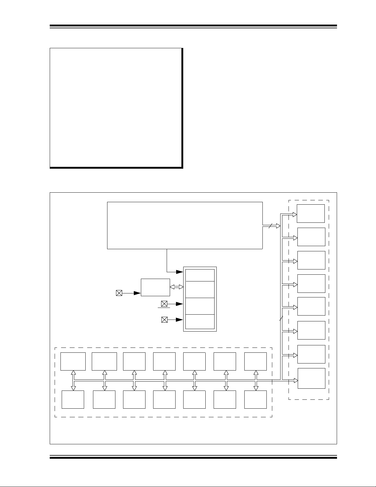
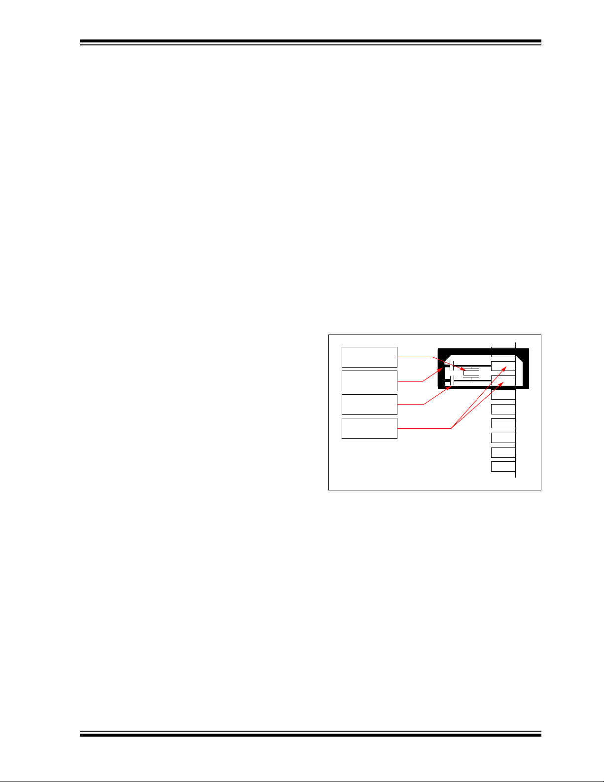
PORTA
Power-up
Timer
Oscillator
Start-up
OSC1/CLKI
MCLR
VDD, VSS
UART1,
Timing
Generation
ECAN1
(2)
I2C1,
ADC
Timers
Input
Capture
Output
Compare
AV
DD, AVSS
UART2
SPI2
SPI1,
Watchdog
Timer
POR/BOR
CRC
I2C2
QEI1
(1)
PWM
(1)
Remappable
Pins
Note 1: This feature or peripheral is only available on dsPIC33EPXXXMC20X/50X and PIC24EPXXXMC20X devices.
2: This feature or peripheral is only available on dsPIC33EPXXXGP/MC50X devices.
Op amp/
Comparator
CTMU
PTG
CPU
Refer to Figure 3-1 for CPU diagram details.
16
16
PORTA
PORTC
PORTD
PORTE
PORTF
PORTG
PORTS
Peripheral Modules
Timer
1.0 DEVICE OVERVIEW
This document contains device-specific information for
the dsPIC33EPXXXGP50X, dsPIC33EPXXXMC20X/
Note 1: This data sheet summarizes the fea-
tures of the dsPIC33EPXXXGP50X,
dsPIC33EPXXXMC20X/50X, and
PIC24EPXXXGP/MC20X families of
devices. It is not intended to be a comprehensive resource. To complement
the information in this data sheet, refer
to the related section of the “dsPIC33E/
PIC24E Family Reference Manual”,
which is available from the Microchip
50X, and PIC24EPXXXGP/MC20X Digital Signal
Controller (DSC) and Microcontroller (MCU) devices.
dsPIC33EPXXXMC20X/50X and dsPIC33EPXXXGP50X
devices contain extensive Digital Signal Processor (DSP)
functionality with a high-performance 16-bit MCU
architecture.
Figure 1-1 shows a general block diagram of the core
and peripheral modules. Ta b le 1- 1 lists the functions of
the various pins shown in the pinout diagrams.
web site (www.microchip.com)
2: Some registers and associated bits
described in this section may not be
available on all devices. Refer to
Section 4.0 “Memory Organization” in
this data sheet for device-specific register
and bit information.
FIGURE 1-1: dsPIC33EPXXXGP50X, dsPIC33EPXXXMC20X/50X, AND PIC24EPXXXGP/MC20X
BLOCK DIAGRAM
© 2011-2012 Microchip Technology Inc. Preliminary DS70657E-page 23

dsPIC33EPXXXGP50X, dsPIC33EPXXXMC20X/50X, AND PIC24EPXXXGP/MC20X
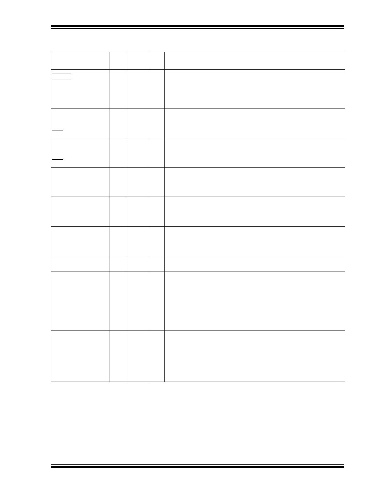
TABLE 1-1: PINOUT I/O DESCRIPTIONS
Pin
Pin Name
AN0-AN15 I Analog No Analog input channels.
CLKI
CLKO
OSC1
OSC2
REFCLKO O — Yes Reference clock output.
IC1-IC4 I ST Yes Capture inputs 1 through 4.
OCFA
OCFB
OC1-OC4
INT0
INT1
INT2
RA0-RA4, RA7-RA12 I/O ST No PORTA is a bidirectional I/O port.
RB0-RB15 I/O ST No PORTB is a bidirectional I/O port.
RC0-RC13, RC15 I/O ST No PORTC is a bidirectional I/O port.
RD5, RD6, RD8 I/O ST No PORTD is a bidirectional I/O port.
RE12-RE15 I/O ST No PORTE is a bidirectional I/O port.
RF0, RF1 I/O ST No PORTF is a bidirectional I/O port.
RG6-RG9 I/O ST No PORTG is a bidirectional I/O port.
T1CK
T2CK
T3CK
T4CK
T5CK
CTPLS
CTED1
CTED2
U1CTS
U1RTS
U1RX
U1TX
BCLK1
Legend: CMOS = CMOS compatible input or output Analog = Analog input P = Power
Note 1: This pin is available on dsPIC33EPXXXMC20X/50X and PIC24EPXXXMC20X devices only.
2: This pin is available on dsPIC33EPXXXGP/MC50X devices only.
3: This is the default Fault on Reset for dsPIC33EPXXXMC20X/50X and PIC24EPXXXMC20X devices. See
4: Not all pins are available in all packages variants. See the “Pin Diagrams” section for pin availability.
(4)
ST = Schmitt Trigger input with CMOS levels O = Output I = Input
PPS = Peripheral Pin Select TTL = TTL input buffer
Section 16.0 “High-Speed PWM Module (dsPIC33EPXXXMC20X/50X and PIC24EPXXXMC20X
Devices Only)” for more information.
Typ e
I
O
I
I/O
I
I
O
I
I
I
I
I
I
I
I
O
I
I
I
O
I
O
O
Buffer
Type
ST/
CMOS
—
ST/
CMOS
—
ST
ST
—
ST
ST
ST
ST
ST
ST
ST
ST
ST
ST
ST
ST
—
ST
—
ST
PPS Description
NoNoExternal clock source input. Always associated with OSC1 pin function.
Oscillator crystal output. Connects to crystal or resonator in Crystal
Oscillator mode. Optionally functions as CLKO in RC and EC modes.
Always associated with OSC2 pin function.
NoNoOscillator crystal input. ST buffer when configured in RC mode; CMOS
otherwise.
Oscillator crystal output. Connects to crystal or resonator in Crystal
Oscillator mode. Optionally functions as CLKO in RC and EC modes.
Yes
Compare Fault A input (for Compare channels).
No
Compare Fault B input (for Compare channels).
Yes
Compare outputs 1 through 4.
No
External interrupt 0.
Yes
External interrupt 1.
Yes
External interrupt 2.
No
Timer1 external clock input.
Yes
Timer2 external clock input.
No
Timer3 external clock input.
No
Timer4 external clock input.
No
Timer5 external clock input.
No
CTMU pulse output.
No
CTMU external edge input 1.
No
CTMU external edge input 2.
No
UART1 clear to send.
No
UART1 ready to send.
Yes
UART1 receive.
Yes
UART1 transmit.
No
UART1 IrDA baud clock output.
DS70657E-page 24 Preliminary © 2011-2012 Microchip Technology Inc.
dsPIC33EPXXXGP50X, dsPIC33EPXXXMC20X/50X, AND PIC24EPXXXGP/MC20X
TABLE 1-1: PINOUT I/O DESCRIPTIONS (CONTINUED)
Pin
Pin Name
(4)
Typ e
Buffer
Type
PPS Description
U2CTS
U2RTS
U2RX
U2TX
BCLK2
SCK1
SDI1
SDO1
SS1
SCK2
SDI2
SDO2
SS2
SCL1
SDA1
ASCL1
ASDA1
SCL2
SDA2
ASCL2
ASDA2
TMS
TCK
TDI
TDO
(2)
(2)
(1)
, FLT2
(1)
, FLT4
(1,3)
(1)
(1)
(1)
(1)
(1)
(1)
(1)
(1)
(1)
(1)
C1RX
C1TX
FLT1
FLT3
FLT32
DTCMP1-DTCMP3
PWM1L-PWM3L
PWM1H-PWM3H
SYNCI1
SYNCO1
INDX1
HOME1
QEA1
QEB1
CNTCMP1
(1)
(1)
O
O
O
I/O
O
I/O
I/O
O
I/O
I/O
I/O
I/O
I/O
I/O
I/O
I/O
I/O
O
O
O
O
O
O
I
I
I
I
I
I
I
I
I
I
I
I
I
I
I
I
I
ST
ST
ST
ST
ST
ST
ST
ST
ST
ST
ST
ST
ST
ST
ST
ST
ST
ST
ST
ST
—
—
—
—
—
No
No
Yes
Yes
No
No
No
No
No
Yes
Yes
Yes
Yes
No
No
No
No
No
No
No
No
No
No
No
No
ST—Yes
Yes
ST
Yes
ST
ST
ST
ST
ST
ST
ST
ST
—
—
—
—
No
No
Yes
No
No
Yes
Yes
Yes
Yes
Yes
Yes
Yes
UART2 clear to send.
UART2 ready to send.
UART2 receive.
UART2 transmit.
UART2 IrDA baud clock output.
Synchronous serial clock input/output for SPI1.
SPI1 data in.
SPI1 data out.
SPI1 slave synchronization or frame pulse I/O.
Synchronous serial clock input/output for SPI2.
SPI2 data in.
SPI2 data out.
SPI2 slave synchronization or frame pulse I/O.
Synchronous serial clock input/output for I2C1.
Synchronous serial data input/output for I2C1.
Alternate synchronous serial clock input/output for I2C1.
Alternate synchronous serial data input/output for I2C1.
Synchronous serial clock input/output for I2C2.
Synchronous serial data input/output for I2C2.
Alternate synchronous serial clock input/output for I2C2.
Alternate synchronous serial data input/output for I2C2.
JTAG Test mode select pin.
JTAG test clock input pin.
JTAG test data input pin.
JTAG test data output pin.
ECAN1 bus receive pin.
ECAN1 bus transmit pin.
PWM Fault input 1 and 2.
PWM Fault input 3 and 4.
PWM Fault input 32 (Class B Fault).
PWM Dead Time Compensation Input 1 through 3.
PWM Low Output 1 through 3.
PWM High Output 1 through 3.
PWM Synchronization Input 1.
PWM Synchronization Output 1.
Quadrature Encoder Index1 Pulse input.
Quadrature Encoder Home1 Pulse input.
Quadrature Encoder Phase A input in QEI1 mode. Auxiliary Timer
External Clock/Gate input in Timer mode.
Quadrature Encoder Phase B input in QEI1 mode. Auxiliary Timer
External Clock/Gate input in Timer mode.
Quadrature Encoder Compare Output 1.
Legend: CMOS = CMOS compatible input or output Analog = Analog input P = Power
ST = Schmitt Trigger input with CMOS levels O = Output I = Input
PPS = Peripheral Pin Select TTL = TTL input buffer
Note 1: This pin is available on dsPIC33EPXXXMC20X/50X and PIC24EPXXXMC20X devices only.
2: This pin is available on dsPIC33EPXXXGP/MC50X devices only.
3: This is the default Fault on Reset for dsPIC33EPXXXMC20X/50X and PIC24EPXXXMC20X devices. See
Section 16.0 “High-Speed PWM Module (dsPIC33EPXXXMC20X/50X and PIC24EPXXXMC20X
Devices Only)” for more information.
4: Not all pins are available in all packages variants. See the “Pin Diagrams” section for pin availability.
© 2011-2012 Microchip Technology Inc. Preliminary DS70657E-page 25
dsPIC33EPXXXGP50X, dsPIC33EPXXXMC20X/50X, AND PIC24EPXXXGP/MC20X
TABLE 1-1: PINOUT I/O DESCRIPTIONS (CONTINUED)
Pin
Pin Name
(4)
C1IN1C1IN2C1IN1+
OA1OUT
C1OUT
C2IN1C2IN2C2IN1+
OA2OUT
C2OUT
C3IN1C3IN2C3IN1+
OA3OUT
C3OUT
C4IN1C4IN1+
C4OUT
REF1O
CV
CVREF2O
PGED1
PGEC1
PGED2
PGEC2
PGED3
PGEC3
MCLR
AVDD P P No Positive supply for analog modules. This pin must be connected at all
AV
SS P P No Ground reference for analog modules. This pin must be connected at all
DD P — No Positive supply for peripheral logic and I/O pins.
V
V
CAP P — No CPU logic filter capacitor connection.
V
SS P — No Ground reference for logic and I/O pins.
V
REF+ I Analog No Analog voltage reference (high) input.
V
REF- I Analog No Analog voltage reference (low) input.
Legend: CMOS = CMOS compatible input or output Analog = Analog input P = Power
ST = Schmitt Trigger input with CMOS levels O = Output I = Input
PPS = Peripheral Pin Select TTL = TTL input buffer
Note 1: This pin is available on dsPIC33EPXXXMC20X/50X and PIC24EPXXXMC20X devices only.
2: This pin is available on dsPIC33EPXXXGP/MC50X devices only.
3: This is the default Fault on Reset for dsPIC33EPXXXMC20X/50X and PIC24EPXXXMC20X devices. See
Section 16.0 “High-Speed PWM Module (dsPIC33EPXXXMC20X/50X and PIC24EPXXXMC20X
Devices Only)” for more information.
4: Not all pins are available in all packages variants. See the “Pin Diagrams” section for pin availability.
Buffer
Typ e
I
Analog
I
Analog
I
Analog
O
Analog
O
I
Analog
I
Analog
I
Analog
O
Analog
O
I
Analog
I
Analog
I
Analog
O
Analog
O
I
Analog
I
Analog
O
OOAnalog
AnalogNoNo
I/O
I
I/O
I
I/O
I
Type
PPS Description
No
Op amp/Comparator 1 Negative Input 1.
No
Comparator 1 Negative Input 2.
No
Op amp/Comparator 1 Positive Input 1.
No
Op amp 1 Output.
—
Yes
Comparator 1 Output.
No
Op amp/Comparator 2 Negative Input 1.
No
Comparator 2 Negative Input 2.
No
Op amp/Comparator 2 Positive Input 1.
No
Op amp 2 Output.
—
Yes
Comparator 2 Output.
No
Op amp/Comparator 3 Negative Input 1.
No
Comparator 3 Negative Input 2.
No
Op amp/Comparator 3 Positive Input 1.
No
Op amp 3 Output.
—
Yes
Comparator 3 Output.
No
Comparator 4 Negative Input 1.
No
Comparator 4 Positive Input 1.
—
Yes
Comparator 4 Output.
Op amp/Comparator Voltage Reference Output.
Op amp/Comparator Voltage Reference divided by 2 Output.
ST
ST
ST
ST
ST
ST
No
Data I/O pin for programming/debugging communication channel 1.
No
Clock input pin for programming/debugging communication channel 1.
No
Data I/O pin for programming/debugging communication channel 2.
No
Clock input pin for programming/debugging communication channel 2.
No
Data I/O pin for programming/debugging communication channel 3.
No
Clock input pin for programming/debugging communication channel 3.
I/P ST No Master Clear (Reset) input. This pin is an active-low Reset to the
device.
times.
times.
DS70657E-page 26 Preliminary © 2011-2012 Microchip Technology Inc.

dsPIC33EPXXXGP50X, dsPIC33EPXXXMC20X/50X, AND PIC24EPXXXGP/MC20X
2.0 GUIDELINES FOR GETTING STARTED WITH 16-BIT DIGITAL SIGNAL CONTROLLERS AND MICROCONTROLLERS
Note 1: This data sheet summarizes the features
of the dsPIC33EPXXXGP50X,
dsPIC33EPXXXMC20X/50X, and
PIC24EPXXXGP/MC20X families of
devices. It is not intended to be a comprehensive reference source. To complement the information in this data sheet,
refer to the related section of the
“dsPIC33E/PIC24E Family Reference
Manual”, which is available from the
Microchip web site (www.microchip.com)
2: Some registers and associated bits
described in this section may not be
available on all devices. Refer to
Section 4.0 “Memory Organization” in
this data sheet for device-specific register
and bit information.
2.1 Basic Connection Requirements
Getting started with the dsPIC33EPXXXGP50X,
dsPIC33EPXXXMC20X/50X, and
PIC24EPXXXGP/MC20X families requires attention to a
minimal set of device pin connections before proceeding
with development. The following is a list of pin names,
which must always be connected:
DD and VSS pins
• All V
(see Section 2.2 “Decoupling Capacitors”)
• All AV
•V
•MCLR
• PGECx/PGEDx pins used for In-Circuit Serial
• OSC1 and OSC2 pins when external oscillator
Additionally, the following pins may be required:
•V
DD and AVSS pins (regardless if ADC module
is not used)
(see Section 2.2 “Decoupling Capacitors”)
CAP
(see Section 2.3 “CPU Logic Filter Capacitor
Connection (V
pin
(see Section 2.4 “Master Clear (MCLR) Pin”)
Programming™ (ICSP™) and debugging purposes
(see Section 2.5 “ICSP Pins”)
source is used
(see Section 2.6 “External Oscillator Pins”)
REF+/VREF- pins are used when external voltage
reference for ADC module is implemented
Note: The AV
CAP)”)
DD and AVSS pins must be
connected independent of the ADC
voltage reference source.
2.2 Decoupling Capacitors
The use of decoupling capacitors on every pair of
power supply pins, such as V
AVSS is required.
Consider the following criteria when using decoupling
capacitors:
• Value and type of capacitor: Recommendation
of 0.1 µF (100 nF), 10-20V. This capacitor should
be a low-ESR and have resonance frequency in
the range of 20 MHz and higher. It is
recommended to use ceramic capacitors.
• Placement on the printed circuit board: The
decoupling capacitors should be placed as close
to the pins as possible. It is recommended to
place the capacitors on the same side of the
board as the device. If space is constricted, the
capacitor can be placed on another layer on the
PCB using a via; however, ensure that the trace
length from the pin to the capacitor is within
one-quarter inch (6 mm) in length.
• Handling high frequency noise: If the board is
experiencing high frequency noise, above tens of
MHz, add a second ceramic-type capacitor in
parallel to the above described decoupling
capacitor. The value of the second capacitor can
be in the range of 0.01 µF to 0.001 µF. Place this
second capacitor next to the primary decoupling
capacitor. In high-speed circuit designs, consider
implementing a decade pair of capacitances as
close to the power and ground pins as possible.
For example, 0.1 µF in parallel with 0.001 µF.
• Maximizing performance: On the board layout
from the power supply circuit, run the power and
return traces to the decoupling capacitors first,
and then to the device pins. This ensures that the
decoupling capacitors are first in the power chain.
Equally important is to keep the trace length
between the capacitor and the power pins to a
minimum, thereby reducing PCB track
inductance.
DD, VSS, AVDD and
© 2011-2012 Microchip Technology Inc. Preliminary DS70657E-page 27
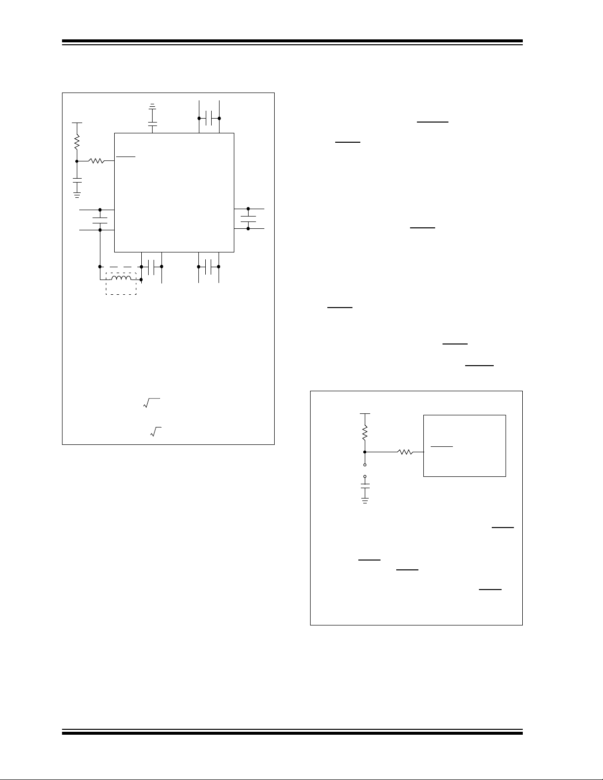
dsPIC33EPXXXGP50X, dsPIC33EPXXXMC20X/50X, AND PIC24EPXXXGP/MC20X
dsPIC33E/PIC24E
VDD
VSS
VDD
VSS
VSS
VDD
AVDD
AVSS
VDD
VSS
0.1 µF
Ceramic
0.1 µF
Ceramic
0.1 µF
Ceramic
0.1 µF
Ceramic
C
R
V
DD
MCLR
0.1 µF
Ceramic
VCAP
L1
(1)
R1
10 µF
Tantalum
Note 1: As an option, instead of a hard-wired connection, an
inductor (L1) can be substituted between V
DD and
AV
DD to improve ADC noise rejection. The inductor
impedance should be less than 1Ω and the inductor
capacity greater than 10 mA.
Where:
f
FCNV
2
--------------=
f
1
2π LC()
-----------------------=
L
1
2πfC()
---------------------
⎝⎠
⎛⎞
2
=
(i.e., ADC conversion rate/2)
Note 1: R ≤ 10 kΩ is recommended. A suggested
starting value is 10 kΩ. Ensure that the MCLR
pin VIH and VIL specifications are met.
2: R1 ≤ 470Ω will limit any current flowing into
MCLR
from the external capacitor C, in the
event of MCLR
pin breakdown, due to
Electrostatic Discharge (ESD) or Electrical
Overstress (EOS). Ensure that the MCLR
pin
V
IH and VIL specifications are met.
C
R1
(2)
R
(1)
VDD
MCLR
dsPIC33EP/PIC24EP
JP
FIGURE 2-1: RECOMMENDED
MINIMUM CONNECTION
The placement of this capacitor should be close to the
CAP pin. It is recommended that the trace length not
V
exceeds one-quarter inch (6 mm). See Section 27.3
“On-Chip Voltage Regulator” for details.
2.4 Master Clear (MCLR) Pin
The MCLR pin provides two specific device
functions:
• Device Reset
• Device Programming and Debugging.
During device programming and debugging, the
resistance and capacitance that can be added to the
pin must be considered. Device programmers and
debuggers drive the MCLR
specific voltage levels (VIH and VIL) and fast signal
transitions must not be adversely affected. Therefore,
specific values of R and C will need to be adjusted
based on the application and PCB requirements.
For example, as shown in Figure 2-2, it is
recommended that the capacitor C, be isolated from
the MCLR
pin during programming and debugging
operations.
Place the components as shown in Figure 2-2 within
one-quarter inch (6 mm) from the MCLR
pin. Consequently,
pin.
CAP)
2.2.1 TANK CAPACITORS
On boards with power traces running longer than six
inches in length, it is suggested to use a tank capacitor
for integrated circuits including DSCs to supply a local
power source. The value of the tank capacitor should
be determined based on the trace resistance that connects the power supply source to the device, and the
maximum current drawn by the device in the application. In other words, select the tank capacitor so that it
meets the acceptable voltage sag at the device. Typical
values range from 4.7 µF to 47 µF.
2.3 CPU Logic Filter Capacitor
A low-ESR (< 1 Ohms) capacitor is required on the
CAP pin, which is used to stabilize the voltage
V
regulator output voltage. The VCAP pin must not be
connected to VDD, and must have a capacitor greater
than 4.7 µF (10 µF is recommended), 16V connected
to ground. The type can be ceramic or tantalum. See
Section 30.0 “Electrical Characteristics” for
additional information.
DS70657E-page 28 Preliminary © 2011-2012 Microchip Technology Inc.
Connection (V
FIGURE 2-2: EXAMPLE OF MCLR PIN
CONNECTIONS
dsPIC33EPXXXGP50X, dsPIC33EPXXXMC20X/50X, AND PIC24EPXXXGP/MC20X
Main Oscillator
Guard Ring
Guard Trace
Oscillator Pins
2.5 ICSP Pins
The PGECx and PGEDx pins are used for ICSP and
debugging purposes. It is recommended to keep the
trace length between the ICSP connector and the ICSP
pins on the device as short as possible. If the ICSP connector is expected to experience an ESD event, a
series resistor is recommended, with the value in the
range of a few tens of Ohms, not to exceed 100 Ohms.
Pull-up resistors, series diodes and capacitors on the
PGECx and PGEDx pins are not recommended as they
will interfere with the programmer/debugger communications to the device. If such discrete components are
an application requirement, they should be removed
from the circuit during programming and debugging.
Alternatively, refer to the AC/DC characteristics and
timing requirements information in the respective
device Flash programming specification for information
on capacitive loading limits and pin input voltage high
IH) and input low (VIL) requirements.
(V
Ensure that the “Communication Channel Select” (i.e.,
PGECx/PGEDx pins) programmed into the device
matches the physical connections for the ICSP to
MPLAB
ICE™.
For more information on ICD 2, ICD 3 and REAL ICE
connection requirements, refer to the following
documents that are available on the Microchip web
site.
• “Using MPLAB
• “MPLAB
• “MPLAB
• “Using MPLAB
®
PICkit™ 3, MPLAB ICD 3, or MPLAB REAL
®
®
®
ICD 3” (poster) DS51765
ICD 3 Design Advisory” DS51764
REAL ICE™ In-Circuit Emulator User’s
Guide” DS51616
®
REAL ICE™ In-Circuit Emulator”
(poster) DS51749
2.6 External Oscillator Pins
Many DSCs have options for at least two oscillators: a
high-frequency primary oscillator and a low-frequency
secondary oscillator. For details, see Section 9.0
“Oscillator Configuration” for details.
The oscillator circuit should be placed on the same
side of the board as the device. Also, place the
oscillator circuit close to the respective oscillator pins,
not exceeding one-half inch (12 mm) distance
between them. The load capacitors should be placed
next to the oscillator itself, on the same side of the
board. Use a grounded copper pour around the
oscillator circuit to isolate them from surrounding
circuits. The grounded copper pour should be routed
directly to the MCU ground. Do not run any signal
traces or power traces inside the ground pour. Also, if
using a two-sided board, avoid any traces on the
other side of the board where the crystal is placed. A
suggested layout is shown in Figure 2-3.
FIGURE 2-3: SUGGESTED PLACEMENT
OF THE OSCILLATOR
CIRCUIT
© 2011-2012 Microchip Technology Inc. Preliminary DS70657E-page 29
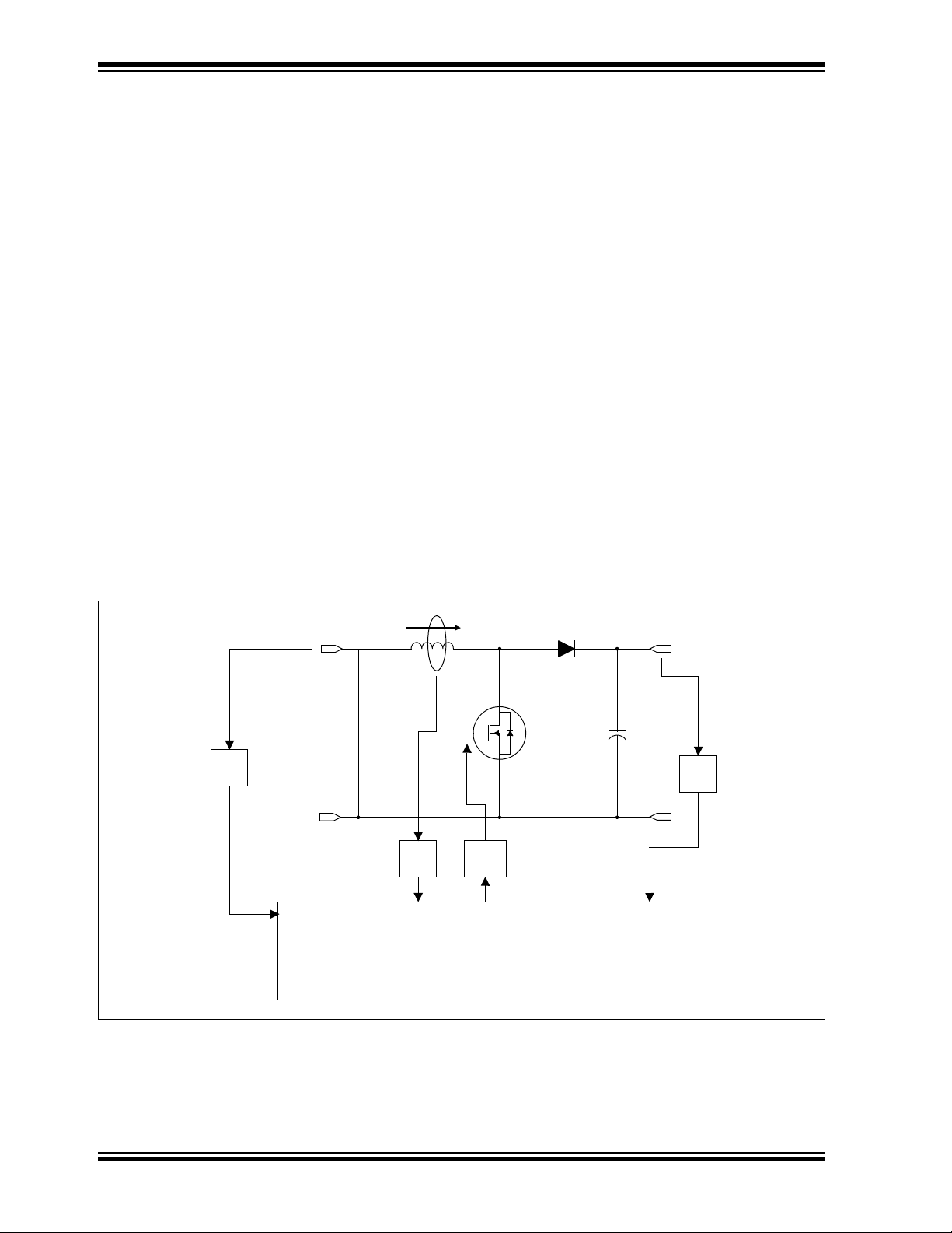
dsPIC33EPXXXGP50X, dsPIC33EPXXXMC20X/50X, AND PIC24EPXXXGP/MC20X
IPFC
VOUTPUT
ADC Channel
Op amp/
ADC Channel
PWM
k
1
k
2
k
3
FET
dsPIC33EP
VINPUT
Comparator Output
Driver
2.7 Oscillator Value Conditions on Device Start-up
If the PLL of the target device is enabled and
configured for the device start-up oscillator, the
maximum oscillator source frequency must be limited
to 3 MHz < F
IN < 5.5 MHz to comply with device PLL
start-up conditions. This means that if the external
oscillator frequency is outside this range, the
application must start-up in the FRC mode first. The
default PLL settings after a POR with an oscillator
frequency outside this range will violate the device
operating speed.
Once the device powers up, the application firmware
can initialize the PLL SFRs, CLKDIV and PLLDBF to a
suitable value, and then perform a clock switch to the
Oscillator + PLL clock source. Note that clock switching
must be enabled in the device Configuration Word.
2.8 Unused I/Os
Unused I/O pins should be configured as outputs and
driven to a logic-low state.
Alternatively, connect a 1k to 10k resistor between V
and unused pins and drive the output to logic low.
SS
2.9 Application Examples
• Induction heating
• Uninterruptable Power Supplies (UPS)
• DC/AC inverters
• Compressor motor control
• Washing machine 3-phase motor control
• BLDC motor control
• Automotive HVAC, cooling fans, fuel pumps
• Stepper motor control
• Audio and fluid sensor monitoring
• Camera lens focus and stability control
• Speech (playback, hands-free kits, answering
machines, VoIP)
• Consumer audio
• Industrial and building control (security systems
and access control)
• Barcode reading
• Networking: LAN switches, gateways
• Data storage device management
• Smart cards and smart card readers
Examples of typical application connections are shown
in Figure 2-4 through Figure 2-8.
FIGURE 2-4: BOOST CONVERTER IMPLEMENTATION
DS70657E-page 30 Preliminary © 2011-2012 Microchip Technology Inc.

dsPIC33EPXXXGP50X, dsPIC33EPXXXMC20X/50X, AND PIC24EPXXXGP/MC20X
k
1
Op amp/
Comparator
k
2
k
7
PWM
PWM
ADC
Channel
ADC
Channel
5V Output
I
5V
12V Input
FET
Driver
dsPIC33EP
k
5
k
4
k
3
k
6
k
7
Op amp/Comparator
Op amp/Comparator
ADC Channel
Op amp/Comparator
ADC
Channel
PWM
PWM
PWM
PWM
PWM
PWM
3.3V Output
12V Input
FET
Driver
FET
Driver
FET
Driver
dsPIC33EP
FIGURE 2-5: SINGLE-PHASE SYNCHRONOUS BUCK CONVERTER
FIGURE 2-6: MULTI-PHASE SYNCHRONOUS BUCK CONVERTER
© 2011-2012 Microchip Technology Inc. Preliminary DS70657E-page 31
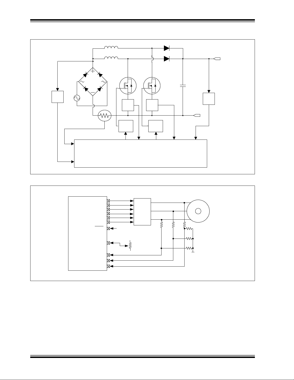
dsPIC33EPXXXGP50X, dsPIC33EPXXXMC20X/50X, AND PIC24EPXXXGP/MC20X
VAC
VOUT+
Op amp/Comparator
PWM
ADC
PWM
|V
AC|
k
4
k
3
FET
dsPIC33EP
Driver
V
OUT-
ADC Channel
FET
Driver
Op amp/
k
1
k
2
Comparator
Channel
Op amp/
Comparator
3-Phase
Inverter
PWM3H
PWM3L
PWM2H
PWM2L
PWM1H
PWM1L
FLTx
Fault
BLDC
dsPIC33EP/PIC24EP
AN3
AN4
AN5
AN2
Demand
Phase Terminal Voltage Feedback
R49 R41 R34
R36
R44
R52
FIGURE 2-7: INTERLEAVED PFC
FIGURE 2-8: BEMF VOLTAGE MEASURED USING THE ADC MODULE
DS70657E-page 32 Preliminary © 2011-2012 Microchip Technology Inc.

dsPIC33EPXXXGP50X, dsPIC33EPXXXMC20X/50X, AND PIC24EPXXXGP/MC20X
3.0 CPU
Note 1: This data sheet summarizes the features
of the dsPIC33EPXXXGP50X,
dsPIC33EPXXXMC20X/50X, and
PIC24EPXXXGP/MC20X families of
devices. It is not intended to be a
comprehensive reference source. To
complement the information in this data
sheet, refer to Section 2. “CPU”
(DS70359) in the “dsPIC33E/PIC24E
Family Reference Manual”, which is
available from the Microchip web site
(www.microchip.com).
2: Some registers and associated bits
described in this section may not be
available on all devices. Refer to
Section 4.0 “Memory Organization” in
this data sheet for device-specific register
and bit information.
The dsPIC33EPXXXGP50X, dsPIC33EPXXXMC20X/
50X, and PIC24EPXXXGP/MC20X CPU have a 16-bit
(data) modified Harvard architecture with an enhanced
instruction set, including significant support for digital
signal processing. The CPU has a 24-bit instruction
word, with a variable length opcode field. The Program
Counter (PC) is 23 bits wide and addresses up to
4M x 24 bits of user program memory space.
An instruction prefetch mechanism helps maintain
throughput and provides predictable execution. Most
instructions execute in a single-cycle effective execution rate, with the exception of instructions that change
the program flow, the double-word move (MOV.D)
instruction, PSV accesses, and the table instructions.
Overhead free program loop constructs are supported
using the DO and REPEAT instructions, both of which
are interruptible at any point.
3.1 Registers
The dsPIC33EPXXXGP50X, dsPIC33EPXXXMC20X/
50X, and PIC24EPXXXGP/MC20X devices have sixteen 16-bit Working registers in the programmer’s
model. Each of the Working registers can act as a data,
address or address offset register. The 16th Working
register (W15) operates as a software Stack Pointer for
interrupts and calls.
3.2 Instruction Set
The instruction set for dsPIC33EPXXXGP50X and
dsPIC33EPXXXMC20X/50X devices has two classes of
instructions: the MCU class of instructions and the DSP
class of instructions. The instruction set for
PIC24EPXXXGP/MC20X devices has the MCU class of
instructions only and does not support DSP instructions.
These two instruction classes are seamlessly integrated
into the architecture and execute from a single execution
unit. The instruction set includes many addressing modes
and was designed for optimum C compiler efficiency.
3.3 Data Space Addressing
The base data space can be addressed as 4K words or
8 Kbytes and is split into two blocks, referred to as X
and Y data memory. Each memory block has its own
independent Address Generation Unit (AGU). The
MCU class of instructions operate solely through the X
memory AGU, which accesses the entire memory map
as one linear data space. On dsPIC33EPXXXMC20X/
50X and dsPIC33EPXXXGP50X devices, certain DSP
instructions operate through the X and Y AGUs to support dual operand reads, which splits the data address
space into two parts. The X and Y data space boundary
is device specific.
The upper 4 Kbytes of the data space memory map can
optionally be mapped into program space at any 16K
program word boundary. The program-to-data-space
mapping feature, known as Program Space Visibility
(PSV), lets any instruction access program space as if
it were data space. Moreover, the Base Data Space
address is used in conjunction with a read or write page
register (DSRPAG or DSWPAG) to form an Extended
Data Space (EDS) address. The EDS can be
addressed as 8 Mwords or 16 Mbytes. Refer to
Section 3. “Data Memory” (DS70595) and Section 4.
“Program Memory” (DS70613) in the “dsPIC33E/
PIC24E Family Reference Manual” for more details on
EDS, PSV and table accesses.
On dsPIC33EPXXXMC20X/50X and
dsPIC33EPXXXGP50X devices, overhead-free
circular buffers (Modulo Addressing) are supported in
both X and Y address spaces. The Modulo Addressing
removes the software boundary-checking overhead for
DSP algorithms. The X AGU circular addressing can be
used with any of the MCU class of instructions. The X
AGU also supports Bit-Reverse Addressing to greatly
simplify input or output data reordering for radix-2 FFT
algorithms. PIC24EPXXXGP/MC20X devices do not
support Modulo and Bit-Reverse Addressing.
3.4 Addressing Modes
The CPU supports these addressing modes:
• Inherent (no operand)
• Relative
•Literal
• Memory Direct
• Register Direct
• Register Indirect
Each instruction is associated with a predefined
Addressing mode group, depending upon its functional
requirements. As many as six Addressing modes are
supported for each instruction.
© 2011-2012 Microchip Technology Inc. Preliminary DS70657E-page 33
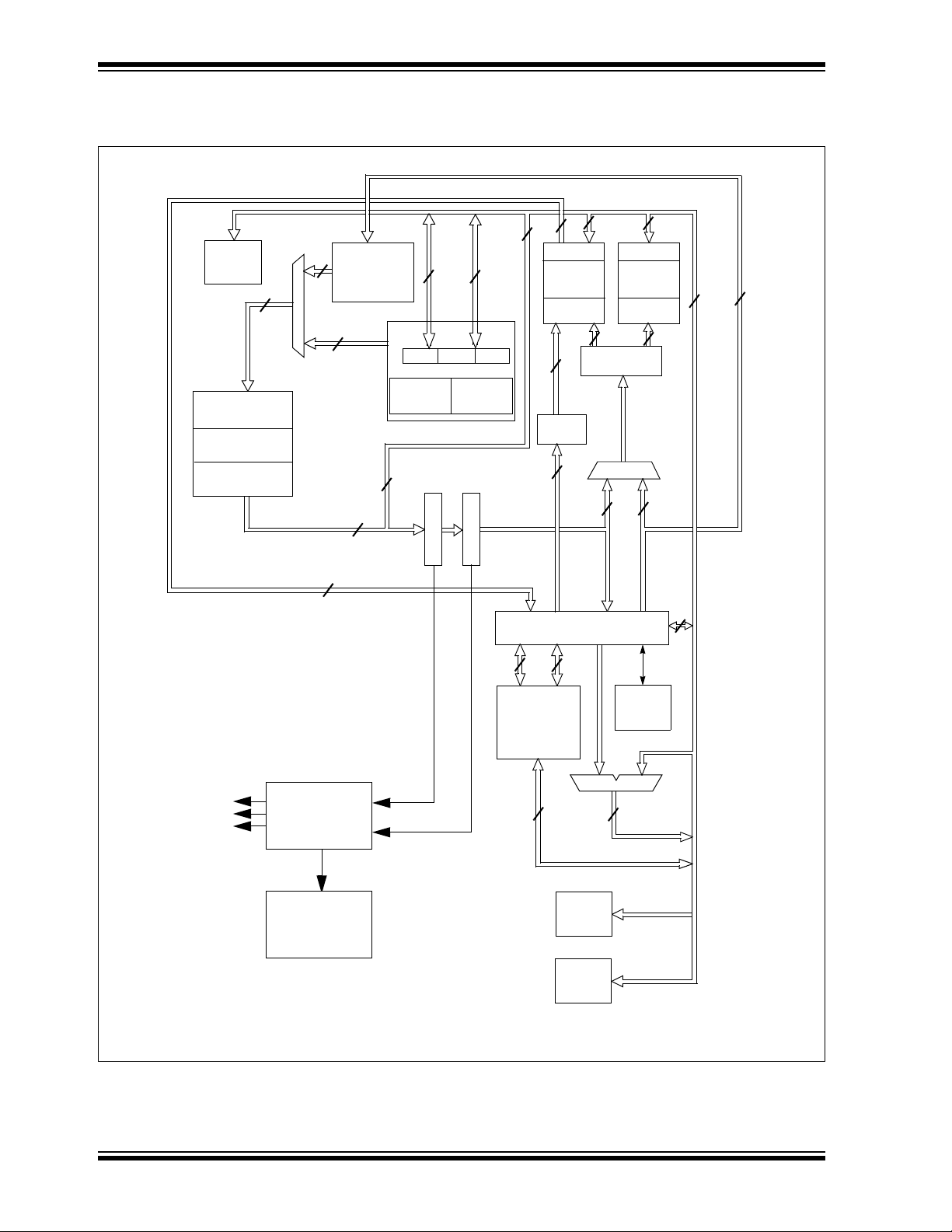
dsPIC33EPXXXGP50X, dsPIC33EPXXXMC20X/50X, AND PIC24EPXXXGP/MC20X
Instruction
Decode and
Control
16
PCH PCL
16
Program Counter
16-bit ALU
24
24
24
24
X Data Bus
IR
PCU
16
16
16
16 x 16
W Register Array
Divide
Support
Engine
(1)
DSP
ROM Latch
16
Y Data Bus
(1)
EA MUX
X RAGU
X WAGU
Y AGU
(1)
16
24
16
16
16
16
16
16
16
8
Interrupt
Controller
PSV and Table
Data Access
Control Block
Stac k
Control
Logic
Loop
Control
Logic
Data LatchData Latch
Y Data
RAM
(1)
X Data
RAM
Address
Latch
Address
Latch
16
Data Latch
16
16
16
X Address Bus
Y Address Bus
24
Literal Data
Program Memory
Address Latch
Power, Reset,
and Oscillator
Control Signals
to Various Blocks
Ports
Peripheral
Modules
Note 1: This feature is not available on PIC24EPXXXGP/MC20X devices.
Modules
FIGURE 3-1: dsPIC33EPXXXGP50X, dsPIC33EPXXXMC20X/50X, AND PIC24EPXXXGP/MC20X
CPU BLOCK DIAGRAM
DS70657E-page 34 Preliminary © 2011-2012 Microchip Technology Inc.

dsPIC33EPXXXGP50X, dsPIC33EPXXXMC20X/50X, AND PIC24EPXXXGP/MC20X
3.5 Programmer’s Model
The programmer’s model for the
dsPIC33EPXXXGP50X, dsPIC33EPXXXMC20X/50X,
and PIC24EPXXXGP/MC20X is shown in Figure 3-2.
All registers in the programmer’s model are memory
mapped and can be manipulated directly by
instructions. Table 3-1 lists a description of each
register.
In addition to the registers contained in the
programmer’s model, the dsPIC33EPXXXGP50X,
dsPIC33EPXXXMC20X/50X, and PIC24EPXXXGP/
MC20X devices contain control registers for Modulo
Addressing (dsPIC33EPXXXMC20X/50X and
dsPIC33EPXXXGP50X devices only), Bit-Reversed
Addressing (dsPIC33EPXXXMC20X/50X and
dsPIC33EPXXXGP50X devices only) and interrupts.
These registers are described in subsequent sections
of this document.
All registers associated with the programmer’s model
are memory mapped, as shown in Ta bl e 4 - 1.
TABLE 3-1: PROGRAMMER’S MODEL REGISTER DESCRIPTIONS
Register(s) Name Description
W0 through W15 Working register array
ACCA, ACCB 40-bit DSP Accumulators
PC 23-bit Program Counter
SR ALU and DSP Engine Status register
SPLIM Stack Pointer Limit Value register
TBLPAG Table Memory Page Address register
DSRPAG Extended Data Space (EDS) Read Page register
DSWPAG Extended Data Space (EDS) Write Page register
RCOUNT REPEAT Loop Count register
DCOUNT
DOSTARTH
DOENDH
CORCON Contains DSP Engine, DO Loop control and trap status bits
Note 1: This register is available on dsPIC33EPXXXMC20X/50X and dsPIC33EPXXXGP50X devices only.
(1)
(1,2)
, DOSTARTL
(1)
, DOENDL
(1,2)
(1)
DO Loop Count register
DO Loop Start Address register (High and Low)
DO Loop End Address register (High and Low)
2: The DOSTARTH and DOSTARTL registers are read-only.
© 2011-2012 Microchip Technology Inc. Preliminary DS70657E-page 35

dsPIC33EPXXXGP50X, dsPIC33EPXXXMC20X/50X, AND PIC24EPXXXGP/MC20X
NOVZ C
TBLPAG
PC23
PC0
7
0
D0D15
Program Counter
Data Table Page Address
Status Register
Working/Address
Registers
DSP Operand
Registers
W0 (WREG)
W1
W2
W3
W4
W5
W6
W7
W8
W9
W10
W11
W12
W13
Frame Pointer/W14
Stack Pointer/W15*
DSP Address
Registers
AD39 AD0
AD31
DSP
Accumulators
(1)
ACCA
ACCB
DSRPAG
9
0
RA
0
OA
(1)OB(1)SA(1)SB(1)
RCOUNT
15
0
Repeat Loop Counter
DCOUNT
15 0
DO Loop Counter and Stack
(1)
DOSTART
23 0
DO Loop Start Address and Stack
(1)
0
DOEND
DO Loop End Address and Stack
(1)
IPL2 IPL1
SPLIM*
Stack Pointer Limit
AD15
23
0
SRL
IPL0
PUSH.s and POP.s shadows
Nested DO Stack
0
0
OAB
(1)
SAB
(1)
X Data Space Read Page Address
DA
(1)
DC
0
0
0
0
DSWPAG
X Data Space Write Page Address
8
0
Note 1: This feature or bit is available on dsPIC33EPXXXMC20X/50X and dsPIC33EPXXXGP50X devices only.
CORCON
15
0
CPU Core Control Register
FIGURE 3-2: PROGRAMMER’S MODEL
DS70657E-page 36 Preliminary © 2011-2012 Microchip Technology Inc.

dsPIC33EPXXXGP50X, dsPIC33EPXXXMC20X/50X, AND PIC24EPXXXGP/MC20X
3.6 CPU Resources
Many useful resources are provided on the main product page of the Microchip web site for the devices listed
in this data sheet. This product page, which can be
accessed using this link, contains the latest updates
and additional information.
Note: In the event you are not able to access the
product page using the link above, enter
this URL in your browser:
http://www.microchip.com/wwwproducts/
Devices.aspx?dDocName=en555464
3.6.1 KEY RESOURCES
• Section 2. “CPU” (DS70359)
• Code Samples
• Application Notes
• Software Libraries
• Webinars
• All related dsPIC33E/PIC24E Family Reference
Manuals Sections
• Development Tools
© 2011-2012 Microchip Technology Inc. Preliminary DS70657E-page 37

dsPIC33EPXXXGP50X, dsPIC33EPXXXMC20X/50X, AND PIC24EPXXXGP/MC20X
3.7 CPU Control Registers
REGISTER 3-1: SR: CPU STATUS REGISTER
R/W-0 R/W-0 R/W-0 R/W-0 R/C-0 R/C-0 R -0 R/W-0
(1)
OA
bit 15 bit 8
OB
(1)
SA
(1,4)
SB
(1,4)
OAB
(1)
SAB
(1)
DA
(1)
DC
R/W-0
(2,3)
R/W-0
(2,3)
R/W-0
(2,3)
R-0 R/W-0 R/W-0 R/W-0 R/W-0
IPL<2:0> RA N OV Z C
bit 7 bit 0
Legend: U = Unimplemented bit, read as ‘0’
R = Readable bit W = Writable bit C = Clearable bit
-n = Value at POR ‘1’= Bit is set ‘0’ = Bit is cleared x = Bit is unknown
bit 15 OA: Accumulator A Overflow Status bit
(1)
1 = Accumulator A has overflowed
0 = Accumulator A has not overflowed
bit 14 OB: Accumulator B Overflow Status bit
(1)
1 = Accumulator B has overflowed
0 = Accumulator B has not overflowed
bit 13 SA: Accumulator A Saturation ‘Sticky’ Status bit
(1,4)
1 = Accumulator A is saturated or has been saturated at some time
0 = Accumulator A is not saturated
bit 12 SB: Accumulator B Saturation ‘Sticky’ Status bit
(1,4)
1 = Accumulator B is saturated or has been saturated at some time
0 = Accumulator B is not saturated
bit 11 OAB: OA || OB Combined Accumulator Overflow Status bit
(1)
1 = Accumulators A or B have overflowed
0 = Neither Accumulators A or B have overflowed
bit 10 SAB: SA || SB Combined Accumulator ‘Sticky’ Status bit
(1)
1 = Accumulators A or B are saturated or have been saturated at some time
0 = Neither Accumulator A or B are saturated
bit 9 DA: DO Loop Active bit
(1)
1 = DO loop in progress
0 = DO loop not in progress
bit 8 DC: MCU ALU Half Carry/Borrow
bit
1 = A carry-out from the 4th low order bit (for byte-sized data) or 8th low order bit (for word-sized data)
of the result occurred
0 = No carry-out from the 4th low order bit (for byte-sized data) or 8th low order bit (for word-sized
data) of the result occurred
Note 1: This bit is available on dsPIC33EPXXXMC20X/50X and dsPIC33EPXXXGP50X devices only.
2: The IPL<2:0> bits are concatenated with the IPL<3> bit (CORCON<3>) to form the CPU Interrupt Priority
Level. The value in parentheses indicates the IPL, if IPL<3> = 1. User interrupts are disabled when
IPL<3> = 1.
3: The IPL<2:0> Status bits are read only when the NSTDIS bit (INTCON1<15>) = 1.
4: A data write to the SR register can modify the SA and SB bits by either a data write to SA and SB or by
clearing the SAB bit. To avoid a possible SA or SB bit write race condition, the SA and SB bits should not
be modified using bit operations.
DS70657E-page 38 Preliminary © 2011-2012 Microchip Technology Inc.

dsPIC33EPXXXGP50X, dsPIC33EPXXXMC20X/50X, AND PIC24EPXXXGP/MC20X
REGISTER 3-1: SR: CPU STATUS REGISTER (CONTINUED)
bit 7-5 IPL<2:0>: CPU Interrupt Priority Level Status bits
111 = CPU Interrupt Priority Level is 7 (15). User interrupts disabled
110 = CPU Interrupt Priority Level is 6 (14)
101 = CPU Interrupt Priority Level is 5 (13)
100 = CPU Interrupt Priority Level is 4 (12)
011 = CPU Interrupt Priority Level is 3 (11)
010 = CPU Interrupt Priority Level is 2 (10)
001 = CPU Interrupt Priority Level is 1 (9)
000 = CPU Interrupt Priority Level is 0 (8)
bit 4 RA: REPEAT Loop Active bit
1 = REPEAT loop in progress
0 = REPEAT loop not in progress
bit 3 N: MCU ALU Negative bit
1 = Result was negative
0 = Result was non-negative (zero or positive)
bit 2 OV: MCU ALU Overflow bit
This bit is used for signed arithmetic (2’s complement). It indicates an overflow of the magnitude that
causes the sign bit to change state.
1 = Overflow occurred for signed arithmetic (in this arithmetic operation)
0 = No overflow occurred
bit 1 Z: MCU ALU Zero bit
1 = An operation that affects the Z bit has set it at some time in the past
0 = The most recent operation that affects the Z bit has cleared it (i.e., a non-zero result)
bit 0 C: MCU ALU Carry/Borrow
1 = A carry-out from the Most Significant bit of the result occurred
0 = No carry-out from the Most Significant bit of the result occurred
bit
(1,2)
Note 1: This bit is available on dsPIC33EPXXXMC20X/50X and dsPIC33EPXXXGP50X devices only.
2: The IPL<2:0> bits are concatenated with the IPL<3> bit (CORCON<3>) to form the CPU Interrupt Priority
Level. The value in parentheses indicates the IPL, if IPL<3> = 1. User interrupts are disabled when
IPL<3> = 1.
3: The IPL<2:0> Status bits are read only when the NSTDIS bit (INTCON1<15>) = 1.
4: A data write to the SR register can modify the SA and SB bits by either a data write to SA and SB or by
clearing the SAB bit. To avoid a possible SA or SB bit write race condition, the SA and SB bits should not
be modified using bit operations.
© 2011-2012 Microchip Technology Inc. Preliminary DS70657E-page 39

dsPIC33EPXXXGP50X, dsPIC33EPXXXMC20X/50X, AND PIC24EPXXXGP/MC20X
REGISTER 3-2: CORCON: CORE CONTROL REGISTER
R/W-0 U-0 R/W-0 R/W-0 R/W-0 R-0 R-0 R-0
VAR
— US<1:0>
(1)
bit 15 bit 8
R/W-0 R/W-0 R/W-1 R/W-0 R/C-0 R-0 R/W-0 R/W-0
SATA
(1)
SATB
(1)
SATDW
(1)
ACCSAT
(1)
bit 7 bit 0
Legend:
R = Readable bit W = Writable bit U = Unimplemented bit, read as ‘0’
-n = Value at POR ‘1’ = Bit is set ‘0’ = Bit is cleared x = Bit is unknown
bit 15 VAR: Variable Exception Processing Latency Control bit
1 = Variable exception processing enabled
0 = Fixed exception processing enabled
bit 14 Unimplemented: Read as ‘0’
bit 13-12 US<1:0>: DSP Multiply Unsigned/Signed Control bits
11 = Reserved
10 = DSP engine multiplies are mixed-sign
01 = DSP engine multiplies are unsigned
00 = DSP engine multiplies are signed
bit 11 EDT: Early DO Loop Termination Control bit
1 = Terminate executing DO loop at end of current loop iteration
0 = No effect
bit 10-8 DL<2:0>: DO Loop Nesting Level Status bits
111 = 7 DO loops active
•
•
•
001 = 1 DO loop active
000 = 0 DO loops active
bit 7 SATA: ACCA Saturation Enable bit
(1)
1 = Accumulator A saturation enabled
0 = Accumulator A saturation disabled
bit 6 SATB: ACCB Saturation Enable bit
(1)
1 = Accumulator B saturation enabled
0 = Accumulator B saturation disabled
bit 5 SATDW: Data Space Write from DSP Engine Saturation Enable bit
1 = Data space write saturation enabled
0 = Data space write saturation disabled
bit 4 ACCSAT: Accumulator Saturation Mode Select bit
1 = 9.31 saturation (super saturation)
0 = 1.31 saturation (normal saturation)
bit 3 IPL3: CPU Interrupt Priority Level Status bit 3
1 = CPU interrupt priority level is greater than 7
0 = CPU interrupt priority level is 7 or less
(1,2)
(1)
EDT
IPL3
(3)
(1,2)
(3)
(1)
(1)
DL<2:0>
SFA RND
(1)
(1)
(1)
IF
(1)
Note 1: This bit is available on dsPIC33EPXXXMC20X/50X and dsPIC33EPXXXGP50X devices only.
2: This bit is always read as ‘0’.
3: The IPL3 bit is concatenated with the IPL<2:0> bits (SR<7:5>) to form the CPU interrupt priority level.
DS70657E-page 40 Preliminary © 2011-2012 Microchip Technology Inc.

dsPIC33EPXXXGP50X, dsPIC33EPXXXMC20X/50X, AND PIC24EPXXXGP/MC20X
REGISTER 3-2: CORCON: CORE CONTROL REGISTER (CONTINUED)
bit 2 SFA: Stack Frame Active Status bit
1 = Stack frame is active. W14 and W15 address 0x0000 to 0xFFFF, regardless of DSRPAG and DSW-
PAG values
0 = Stack frame is not active. W14 and W15 address of EDS or Base Data Space
bit 1 RND: Rounding Mode Select bit
1 = Biased (conventional) rounding enabled
0 = Unbiased (convergent) rounding enabled
bit 0 IF: Integer or Fractional Multiplier Mode Select bit
1 = Integer mode enabled for DSP multiply
0 = Fractional mode enabled for DSP multiply
Note 1: This bit is available on dsPIC33EPXXXMC20X/50X and dsPIC33EPXXXGP50X devices only.
2: This bit is always read as ‘0’.
3: The IPL3 bit is concatenated with the IPL<2:0> bits (SR<7:5>) to form the CPU interrupt priority level.
(1)
(1)
© 2011-2012 Microchip Technology Inc. Preliminary DS70657E-page 41

dsPIC33EPXXXGP50X, dsPIC33EPXXXMC20X/50X, AND PIC24EPXXXGP/MC20X
3.8 Arithmetic Logic Unit (ALU)
The dsPIC33EPXXXGP50X, dsPIC33EPXXXMC20X/
50X, and PIC24EPXXXGP/MC20X ALU is 16 bits wide
and is capable of addition, subtraction, bit shifts and
logic operations. Unless otherwise mentioned,
arithmetic operations are two’s complement in nature.
Depending on the operation, the ALU can affect the
values of the Carry (C), Zero (Z), Negative (N),
Overflow (OV) and Digit Carry (DC) Status bits in the
SR register. The C and DC Status bits operate as
and Digit Borrow bits, respectively, for
Borrow
subtraction operations.
The ALU can perform 8-bit or 16-bit operations,
depending on the mode of the instruction that is used.
Data for the ALU operation can come from the W
register array or data memory, depending on the
addressing mode of the instruction. Likewise, output
data from the ALU can be written to the W register array
or a data memory location.
Refer to the “16-bit MCU and DSC Programmer’s
Reference Manual” (DS70157) for information on the
SR bits affected by each instruction.
The core CPU incorporates hardware support for both
multiplication and division. This includes a dedicated
hardware multiplier and support hardware for 16-bit
divisor division.
3.8.1 MULTIPLIER
Using the high-speed 17-bit x 17-bit multiplier, the ALU
supports unsigned, signed, or mixed-sign operation in
several MCU multiplication modes:
• 16-bit x 16-bit signed
• 16-bit x 16-bit unsigned
• 16-bit signed x 5-bit (literal) unsigned
• 16-bit signed x 16-bit unsigned
• 16-bit unsigned x 5-bit (literal) unsigned
• 16-bit unsigned x 16-bit signed
• 8-bit unsigned x 8-bit unsigned
3.8.2 DIVIDER
The divide block supports 32-bit/16-bit and 16-bit/16-bit
signed and unsigned integer divide operations with the
following data sizes:
• 32-bit signed/16-bit signed divide
• 32-bit unsigned/16-bit unsigned divide
• 16-bit signed/16-bit signed divide
• 16-bit unsigned/16-bit unsigned divide
The quotient for all divide instructions ends up in W0
and the remainder in W1. 16-bit signed and unsigned
DIV instructions can specify any W register for both
the 16-bit divisor (Wn) and any W register (aligned)
pair (W(m + 1):Wm) for the 32-bit dividend. The divide
algorithm takes one cycle per bit of divisor, so both
32-bit/16-bit and 16-bit/16-bit instructions take the
same number of cycles to execute.
3.9 DSP Engine (dsPIC33EPXXXMC20X/50X and dsPIC33EPXXXGP50X Devices Only)
The DSP engine consists of a high-speed 17-bit x
17-bit multiplier, a 40-bit barrel shifter and a 40-bit
adder/subtracter (with two target accumulators, round
and saturation logic).
The DSP engine can also perform inherent accumulator-to-accumulator operations that require no additional
data. These instructions are ADD, SUB and NEG.
The DSP engine has options selected through bits in
the CPU Core Control register (CORCON), as listed
below:
• Fractional or integer DSP multiply (IF)
• Signed, unsigned, or mixed-sign DSP multiply (US)
• Conventional or convergent rounding (RND)
• Automatic saturation on/off for ACCA (SATA)
• Automatic saturation on/off for ACCB (SATB)
• Automatic saturation on/off for writes to data
memory (SATDW)
• Accumulator Saturation mode selection
(ACCSAT)
TABLE 3-2: DSP INSTRUCTIONS
SUMMARY
Instruction
CLR A = 0
ED A = (x – y)
EDAC A = A + (x – y)
MAC A = A + (x • y) Ye s
MAC A = A + x
MOVSAC No change in A Yes
MPY A = x • y No
MPY A = x
MPY.N A = – x • y No
MSC A = A – x • y Yes
Algebraic
Operation
2
2
2
2
ACC Write
Back
Yes
No
No
No
No
DS70657E-page 42 Preliminary © 2011-2012 Microchip Technology Inc.

dsPIC33EPXXXGP50X, dsPIC33EPXXXMC20X/50X, AND PIC24EPXXXGP/MC20X
Reset Address
0x000000
0x000002
Write
User Program
Flash Memory
0x0057EC
0x0057EA
(11K instructions)
0x800000
0xFA0000
Latches
0xFA0002
0xFA0004
DEVID
0xFEFFFE
0xFF0000
0xFFFFFE
0xF9FFFE
Unimplemented
(Read ‘
0
’s)
GOTO
Instruction
0x000004
Reserved
0x7FFFFE
Reserved
0x000200
0x0001FE
Interrupt Vector Table
Configuration Memory Space
User Memory Space
Flash Configuration
Bytes
0x005800
0x0057FE
Reserved
0xFF0002
Note 1: Memory areas are not shown to scale.
2: On reset, these bits are automatically copied into the device Configuration Shadow registers.
0xFF0004
Reserved
0x800FF8
0x800FF6
0x801000
0x800FFE
USERID
4.0 MEMORY ORGANIZATION
Note: This data sheet summarizes the features
of the dsPIC33EPXXXGP50X,
dsPIC33EPXXXMC20X/50X, and
PIC24EPXXXGP/MC20X families of
devices. It is not intended to be a comprehensive reference source. To complement
the information in this data sheet, refer to
Section 4. “Program Memory”
(DS70613) of the “dsPIC33E/PIC24E
Family Reference Manual”, which is avail-
able from the Microchip web site
(www.microchip.com).
The dsPIC33EPXXXGP50X, dsPIC33EPXXXMC20X/
50X, and PIC24EPXXXGP/MC20X architecture
features separate program and data memory spaces
and buses. This architecture also allows the direct
4.1 Program Address Space
The program address memory space of the
dsPIC33EPXXXGP50X, dsPIC33EPXXXMC20X/50X,
and PIC24EPXXXGP/MC20X devices is 4M
instructions. The space is addressable by a 24-bit
value derived either from the 23-bit PC during program
execution, or from table operation or data space
remapping as described in Section 4.8 “Interfacing
Program and Data Memory Spaces”.
User application access to the program memory space
is restricted to the lower half of the address range
(0x000000 to 0x7FFFFF). The exception is the use of
TBLRD operations, which use TBLPAG<7> to read
Device ID sections of the configuration memory space.
The program memory maps, which are presented by
device family and memory size, are shown in
Figure 4-1 through Figure 4-5.
access of program memory from the data space during
code execution.
FIGURE 4-1: PROGRAM MEMORY MAP FOR dsPIC33EP32GP50X, dsPIC33EP32MC20X/50X,
AND PIC24EP32GP/MC20X DEVICES
(1)
© 2011-2012 Microchip Technology Inc. Preliminary DS70657E-page 43

dsPIC33EPXXXGP50X, dsPIC33EPXXXMC20X/50X, AND PIC24EPXXXGP/MC20X
Reset Address
0x000000
0x000002
Write
User Program
Flash Memory
0x00AFEC
0x00AFEA
(22K instructions)
0x800000
0xFA0000
Latches
0xFA0002
0xFA0004
DEVID
0xFEFFFE
0xFF0000
0xFFFFFE
0xF9FFFE
Unimplemented
(Read ‘
0
’s)
GOTO
Instruction
0x000004
Reserved
0x7FFFFE
Reserved
0x000200
0x0001FE
Interrupt Vector Table
Configuration Memory Space
User Memory Space
Flash Configuration
Bytes
0x00B000
0x00AFFE
Reserved
0xFF0002
Note 1: Memory areas are not shown to scale.
2: On reset, these bits are automatically copied into the device Configuration Shadow registers.
0xFF0004
Reserved
0x800FF8
0x800FF6
0x801000
0x800FFE
USERID
FIGURE 4-2: PROGRAM MEMORY MAP FOR dsPIC33EP64GP50X, dsPIC33EP64MC20X/50X,
AND PIC24EP64GP/MC20X DEVICES
(1)
DS70657E-page 44 Preliminary © 2011-2012 Microchip Technology Inc.

dsPIC33EPXXXGP50X, dsPIC33EPXXXMC20X/50X, AND PIC24EPXXXGP/MC20X
Reset Address
0x000000
0x000002
Write
User Program
Flash Memory
0x0157EC
0x0157EA
(44K instructions)
0x800000
0xFA0000
Latches
0xFA0002
0xFA0004
DEVID
0xFEFFFE
0xFF0000
0xFFFFFE
0xF9FFFE
Unimplemented
(Read ‘
0
’s)
GOTO
Instruction
0x000004
Reserved
0x7FFFFE
Reserved
0x000200
0x0001FE
Interrupt Vector Table
Configuration Memory Space
User Memory Space
Flash Configuration
Bytes
0x015800
0x0157FE
Reserved
0xFF0002
Note 1: Memory areas are not shown to scale.
2: On reset, these bits are automatically copied into the device Configuration Shadow registers.
0xFF0004
Reserved
0x800FF8
0x800FF6
0x801000
0x800FFE
USERID
FIGURE 4-3: PROGRAM MEMORY MAP FOR dsPIC33EP128GP50X, dsPIC33EP128MC20X/50X,
AND PIC24EP128GP/MC20X DEVICES
(1)
© 2011-2012 Microchip Technology Inc. Preliminary DS70657E-page 45

dsPIC33EPXXXGP50X, dsPIC33EPXXXMC20X/50X, AND PIC24EPXXXGP/MC20X
Reset Address
0x000000
0x000002
Write
User Program
Flash Memory
0x02AFEC
0x02AFEA
(88K instructions)
0x800000
0xFA0000
Latches
0xFA0002
0xFA0004
DEVID
0xFEFFFE
0xFF0000
0xFFFFFE
0xF9FFFE
Unimplemented
(Read ‘
0
’s)
GOTO
Instruction
0x000004
Reserved
0x7FFFFE
Reserved
0x000200
0x0001FE
Interrupt Vector Table
Configuration Memory Space
User Memory Space
Flash Configuration
Bytes
0x02B000
0x02AFFE
Reserved
0xFF0002
Note 1: Memory areas are not shown to scale.
2: On reset, these bits are automatically copied into the device Configuration Shadow registers.
0xFF0004
Reserved
0x800FF8
0x800FF6
0x801000
0x800FFE
USERID
FIGURE 4-4: PROGRAM MEMORY MAP FOR dsPIC33EP256GP50X, dsPIC33EP256MC20X/50X,
AND PIC24EP256GP/MC20X DEVICES
(1)
DS70657E-page 46 Preliminary © 2011-2012 Microchip Technology Inc.

dsPIC33EPXXXGP50X, dsPIC33EPXXXMC20X/50X, AND PIC24EPXXXGP/MC20X
Reset Address
0x000000
0x000002
Write
User Program
Flash Memory
0x0557EC
0x0557EA
(175K instructions)
0x800000
0xFA0000
Latches
0xFA0002
0xFA0004
DEVID
0xFEFFFE
0xFF0000
0xFFFFFE
0xF9FFFE
Unimplemented
(Read ‘
0
’s)
GOTO
Instruction
0x000004
Reserved
0x7FFFFE
Reserved
0x000200
0x0001FE
Interrupt Vector Table
Configuration Memory Space
User Memory Space
Flash Configuration
Bytes
0x055800
0x0557FE
Reserved
0xFF0002
Note 1: Memory areas are not shown to scale.
2: On reset, these bits are automatically copied into the device Configuration Shadow registers.
0xFF0004
Reserved
0x800FF8
0x800FF6
0x801000
0x800FFE
USERID
FIGURE 4-5: PROGRAM MEMORY MAP FOR dsPIC33EP512GP50X, dsPIC33EP512MC20X/50X,
AND PIC24EP512GP/MC20X DEVICES
(1)
© 2011-2012 Microchip Technology Inc. Preliminary DS70657E-page 47
dsPIC33EPXXXGP50X, dsPIC33EPXXXMC20X/50X, AND PIC24EPXXXGP/MC20X
0816
PC Address
0x000000
0x000002
0x000004
0x000006
23
00000000
00000000
00000000
00000000
Program Memory
‘Phantom’ Byte
(read as ‘0’)
least significant word
most significant word
Instruction Width
0x000001
0x000003
0x000005
0x000007
msw
Address (lsw Address)
4.1.1 PROGRAM MEMORY
ORGANIZATION
The program memory space is organized in wordaddressable blocks. Although it is treated as 24 bits
wide, it is more appropriate to think of each address of
the program memory as a lower and upper word, with
the upper byte of the upper word being unimplemented.
The lower word always has an even address, while the
upper word has an odd address (Figure 4-6).
Program memory addresses are always word-aligned
on the lower word, and addresses are incremented or
decremented by two during code execution. This
arrangement provides compatibility with data memory
space addressing and makes data in the program
memory space accessible.
4.1.2 INTERRUPT AND TRAP VECTORS
All dsPIC33EPXXXGP50X, dsPIC33EPXXXMC20X/
50X, and PIC24EPXXXGP/MC20X devices reserve
the addresses between 0x000000 and 0x000200 for
hard-coded program execution vectors. A hardware
Reset vector is provided to redirect code execution
from the default value of the PC on device Reset to the
actual start of code. A GOTO instruction is programmed
by the user application at address 0x000000 of Flash
memory, with the actual address for the start of code at
address 0x000002 of Flash memory.
A more detailed discussion of the interrupt vector
tables is provided in Section 7.1 “Interrupt Vector
Table ”.
FIGURE 4-6: PROGRAM MEMORY ORGANIZATION
DS70657E-page 48 Preliminary © 2011-2012 Microchip Technology Inc.

dsPIC33EPXXXGP50X, dsPIC33EPXXXMC20X/50X, AND PIC24EPXXXGP/MC20X
4.2 Data Address Space
The dsPIC33EPXXXGP50X, dsPIC33EPXXXMC20X/
50X, and PIC24EPXXXGP/MC20X CPU has a
separate 16-bit wide data memory space. The data
space is accessed using separate Address Generation
Units (AGUs) for read and write operations. The data
memory maps, which are presented by device family
and memory size, are shown in Figure 4-7 through
Figure 4-16.
All Effective Addresses (EAs) in the data memory space
are 16 bits wide and point to bytes within the data space.
This arrangement gives a base data space address
range of 8 Kbytes or 4K words.
The base data space address is used in conjunction with
a read or write page register (DSRPAG or DSWPAG) to
form an extended data space, which has a total address
range of 16 MB.
dsPIC33EPXXXGP50X, dsPIC33EPXXXMC20X/50X,
and PIC24EPXXXGP/MC20X devices implement up to
56 Kbytes of data memory. If an EA point to a location
outside of this area, an all-zero word or byte is returned.
4.2.1 DATA SPACE WIDTH
The data memory space is organized in byte
addressable, 16-bit wide blocks. Data is aligned in data
memory and registers as 16-bit words, but all data
space EAs resolve to bytes. The Least Significant
Bytes (LSBs) of each word have even addresses, while
the Most Significant Bytes (MSBs) have odd
addresses.
4.2.2 DATA MEMORY ORGANIZATION
AND ALIGNMENT
To maintain backward compatibility with PIC
devices and improve data space memory usage
efficiency, the dsPIC33EPXXXGP50X,
dsPIC33EPXXXMC20X/50X, and PIC24EPXXXGP/
MC20X instruction set supports both word and byte
operations. As a consequence of byte accessibility, all
effective address calculations are internally scaled to
step through word-aligned memory. For example, the
core recognizes that Post-Modified Register Indirect
Addressing mode [Ws++] results in a value of Ws + 1
for byte operations and Ws + 2 for word operations.
A data byte read, reads the complete word that
contains the byte, using the LSb of any EA to determine
which byte to select. The selected byte is placed onto
the LSB of the data path. That is, data memory and
registers are organized as two parallel byte-wide
entities with shared (word) address decode but
separate write lines. Data byte writes only write to the
corresponding side of the array or register that matches
the byte address.
®
MCU
All word accesses must be aligned to an even address.
Misaligned word data fetches are not supported, so
care must be taken when mixing byte and word
operations, or translating from 8-bit MCU code. If a
misaligned read or write is attempted, an address error
trap is generated. If the error occurred on a read, the
instruction underway is completed. If the error occurred
on a write, the instruction is executed but the write does
not occur. In either case, a trap is then executed,
allowing the system and/or user application to examine
the machine state prior to execution of the address
Fault.
All byte loads into any W register are loaded into the
LSB. The MSB is not modified.
A Sign-Extend instruction (SE) is provided to allow user
applications to translate 8-bit signed data to 16-bit
signed values. Alternatively, for 16-bit unsigned data,
user applications can clear the MSB of any W register
by executing a Zero-Extend (ZE) instruction on the
appropriate address.
4.2.3 SFR SPACE
The first 4 Kbytes of the Near Data Space, from 0x0000
to 0x0FFF, is primarily occupied by Special Function
Registers (SFRs). These are used by the
dsPIC33EPXXXGP50X, dsPIC33EPXXXMC20X/50X,
and PIC24EPXXXGP/MC20X core and peripheral
modules for controlling the operation of the device.
SFRs are distributed among the modules that they
control, and are generally grouped together by module.
Much of the SFR space contains unused addresses;
these are read as ‘0’.
Note: The actual set of peripheral features and
interrupts varies by the device. Refer to
the corresponding device tables and
pinout diagrams for device-specific
information.
4.2.4 NEAR DATA SPACE
The 8 Kbyte area between 0x0000 and 0x1FFF is
referred to as the near data space. Locations in this
space are directly addressable through a 13-bit absolute address field within all memory direct instructions.
Additionally, the whole data space is addressable using
MOV instructions, which support Memory Direct
Addressing mode with a 16-bit address field, or by
using Indirect Addressing mode using a working
register as an Address Pointer.
© 2011-2012 Microchip Technology Inc. Preliminary DS70657E-page 49
dsPIC33EPXXXGP50X, dsPIC33EPXXXMC20X/50X, AND PIC24EPXXXGP/MC20X
0x0000
0x0FFE
0x17FE
0xFFFE
LSB
Address
16 bits
LSBMSB
MSB
Address
0x0001
0x0FFF
0x17FF
0xFFFF
Optionally
Mapped
into Program
Memory Space
0x1FFF 0x1FFE
0x1001
0x1000
0x1801
0x1800
4 Kbyte
SFR Space
4 Kbyte
SRAM Space
0x20000x2001
Space
Data
Near
8 Kbyte
SFR Space
X Data RAM (X)
X Data
Unimplemented (X)
Y Data RAM (Y)
0x80000x8001
Note: Memory areas are not shown to scale.
(PSV)
FIGURE 4-7: DATA MEMORY MAP FOR dsPIC33EP32MC20X/50X AND dsPIC33EP32GP50X
DEVICES
DS70657E-page 50 Preliminary © 2011-2012 Microchip Technology Inc.

dsPIC33EPXXXGP50X, dsPIC33EPXXXMC20X/50X, AND PIC24EPXXXGP/MC20X
0x0000
0x0FFE
0x1FFE
0xFFFE
LSB
Address
16 bits
LSBMSB
MSB
Address
0x0001
0x0FFF
0x1FFF
0xFFFF
Optionally
Mapped
into Program
Memory Space
0x2FFF 0x2FFE
0x1001
0x1000
0x2001
0x2000
4 Kbyte
SFR Space
8 Kbyte
SRAM Space
0x30000x3001
Space
Data
Near
8 Kbyte
SFR Space
X Data RAM (X)
X Data
Unimplemented (X)
Y Data RAM (Y)
0x80000x8001
Note: Memory areas are not shown to scale.
(PSV)
FIGURE 4-8: DATA MEMORY MAP FOR dsPIC33EP64MC20X/50X AND dsPIC33EP64GP50X
DEVICES
© 2011-2012 Microchip Technology Inc. Preliminary DS70657E-page 51
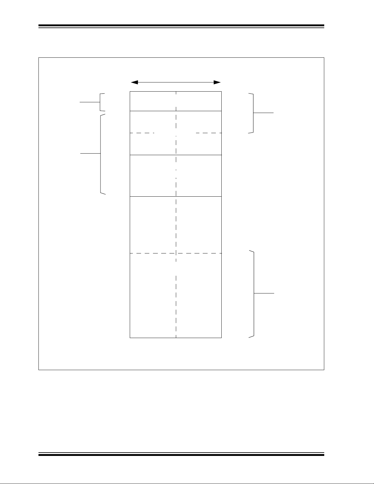
dsPIC33EPXXXGP50X, dsPIC33EPXXXMC20X/50X, AND PIC24EPXXXGP/MC20X
0x0000
0x0FFE
0x2FFE
0xFFFE
LSB
Address
16 bits
LSBMSB
MSB
Address
0x0001
0x0FFF
0x2FFF
0xFFFF
Optionally
Mapped
into Program
Memory Space
0x4FFF 0x4FFE
0x1001
0x1000
0x3001
0x3000
4 Kbyte
SFR Space
16 Kbyte
SRAM Space
0x50000x5001
Space
Data
Near
8 Kbyte
SFR Space
X Data RAM (X)
X Data
Unimplemented (X)
Y Data RAM (Y)
0x80000x8001
Note: Memory areas are not shown to scale.
(PSV)
0x1FFE
0x1FFF
0x2001
0x2000
FIGURE 4-9: DATA MEMORY MAP FOR dsPIC33EP128MC20X/50X AND dsPIC33EP128GP50X
DEVICES
DS70657E-page 52 Preliminary © 2011-2012 Microchip Technology Inc.

dsPIC33EPXXXGP50X, dsPIC33EPXXXMC20X/50X, AND PIC24EPXXXGP/MC20X
0x0000
0x0FFE
0x4FFE
0xFFFE
LSB
Address
16 bits
LSBMSB
MSB
Address
0x0001
0x0FFF
0x4FFF
0xFFFF
Optionally
Mapped
into Program
Memory Space
0x8FFF 0x8FFE
0x1001
0x1000
0x5001
0x5000
4 Kbyte
SFR Space
32 Kbyte
SRAM Space
0x90000x9001
Space
Data
Near
8 Kbyte
SFR Space
X Data RAM (X)
X Data
Unimplemented (X)
Y Data RAM (Y)
Note: Memory areas are not shown to scale.
(PSV)
0x1FFE
0x1FFF
0x2001
0x2000
0x7FFE
0x7FFF
0x8001
0x8000
FIGURE 4-10: DATA MEMORY MAP FOR dsPIC33EP256MC20X/50X AND dsPIC33EP256GP50X
DEVICES
© 2011-2012 Microchip Technology Inc. Preliminary DS70657E-page 53

dsPIC33EPXXXGP50X, dsPIC33EPXXXMC20X/50X, AND PIC24EPXXXGP/MC20X
0x0000
0x0FFE
0x7FFE
0xFFFE
LSB
Address
16 bits
LSBMSB
MSB
Address
0x0001
0x0FFF
0x7FFF
0xFFFF
Optionally
Mapped
into Program
Memory Space
0xEFFF 0xEFFE
0x1001
0x1000
0x8001
0x8000
4 Kbyte
SFR Space
48 Kbyte
SRAM Space
0xD0000xD001
Space
Data
Near
8 Kbyte
SFR Space
X Data RAM (X)
X Data
Unimplemented (X)
Note: Memory areas are not shown to scale.
(PSV)
0x1FFE
0x1FFF
0x2001
0x2000
0x8FFE
0x8FFF
0x9001
0x9000
Y Data RAM (Y)
FIGURE 4-11: DATA MEMORY MAP FOR dsPIC33EP512MC20X/50X AND dsPIC33EP512GP50X
DEVICES
DS70657E-page 54 Preliminary © 2011-2012 Microchip Technology Inc.
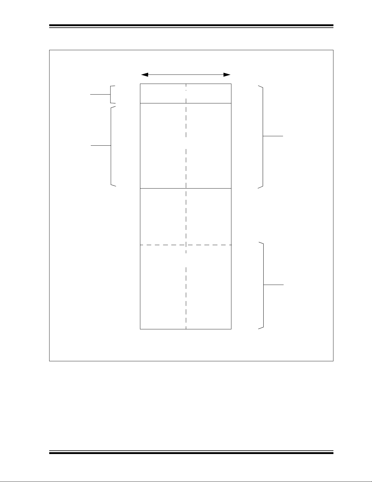
dsPIC33EPXXXGP50X, dsPIC33EPXXXMC20X/50X, AND PIC24EPXXXGP/MC20X
0x0000
0x0FFE
0xFFFE
LSB
Address
16 bits
LSBMSB
MSB
Address
0x0001
0x0FFF
0xFFFF
Optionally
Mapped
into Program
Memory Space
0x1FFF 0x1FFE
0x1001
0x1000
4 Kbyte
SFR Space
4 Kbyte
SRAM Space
0x20000x2001
Space
Data
Near
8 Kbyte
SFR Space
X Data RAM (X)
X Data
Unimplemented (X)
0x80000x8001
Note: Memory areas are not shown to scale.
(PSV)
FIGURE 4-12: DATA MEMORY MAP FOR PIC24EP32GP/MC20X/50X DEVICES
© 2011-2012 Microchip Technology Inc. Preliminary DS70657E-page 55
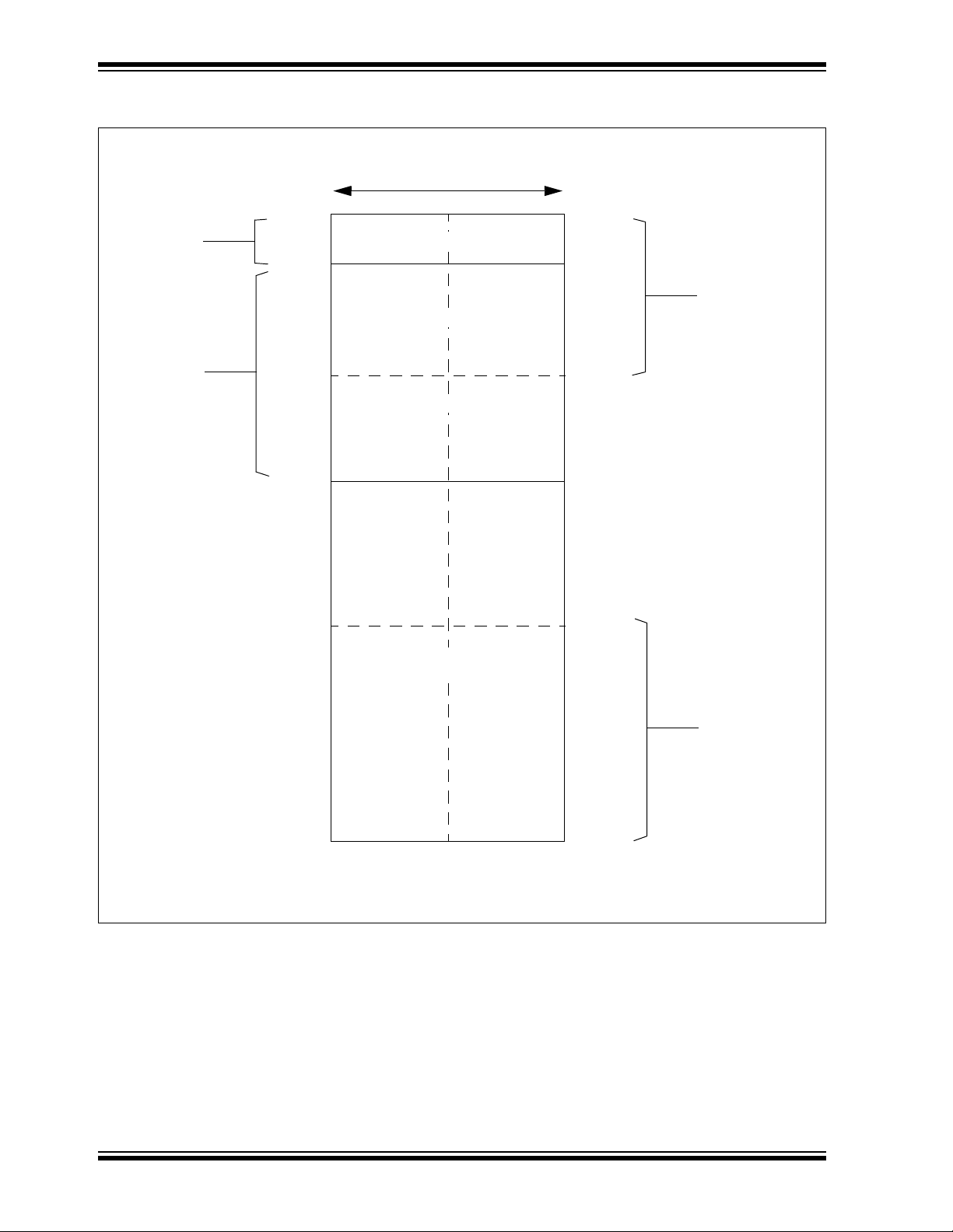
dsPIC33EPXXXGP50X, dsPIC33EPXXXMC20X/50X, AND PIC24EPXXXGP/MC20X
0x0000
0x0FFE
0x1FFE
0xFFFE
LSB
Address
16 bits
LSBMSB
MSB
Address
0x0001
0x0FFF
0x1FFF
0xFFFF
Optionally
Mapped
into Program
Memory Space
0x2FFF 0x2FFE
0x1001
0x1000
0x2001
0x2000
4 Kbyte
SFR Space
8 Kbyte
SRAM Space
0x30000x3001
Space
Data
Near
8 Kbyte
SFR Space
X Data RAM (X)
X Data
Unimplemented (X)
0x80000x8001
Note: Memory areas are not shown to scale.
(PSV)
FIGURE 4-13: DATA MEMORY MAP FOR PIC24EP64GP/MC20X/50X DEVICES
DS70657E-page 56 Preliminary © 2011-2012 Microchip Technology Inc.

dsPIC33EPXXXGP50X, dsPIC33EPXXXMC20X/50X, AND PIC24EPXXXGP/MC20X
0x0000
0x0FFE
0xFFFE
LSB
Address
16 bits
LSBMSB
MSB
Address
0x0001
0x0FFF
0xFFFF
Optionally
Mapped
into Program
Memory Space
0x4FFF 0x4FFE
0x1001
0x1000
4 Kbyte
SFR Space
16 Kbyte
SRAM Space
0x50000x5001
Space
Data
Near
8 Kbyte
SFR Space
X Data RAM (X)
X Data
Unimplemented (X)
0x80000x8001
Note: Memory areas are not shown to scale.
(PSV)
0x1FFE
0x1FFF
0x2001
0x2000
FIGURE 4-14: DATA MEMORY MAP FOR PIC24128GP/MC20X/50X DEVICES
© 2011-2012 Microchip Technology Inc. Preliminary DS70657E-page 57

dsPIC33EPXXXGP50X, dsPIC33EPXXXMC20X/50X, AND PIC24EPXXXGP/MC20X
0x0000
0x0FFE
0xFFFE
LSB
Address
16 bits
LSBMSB
MSB
Address
0x0001
0x0FFF
0xFFFF
Optionally
Mapped
into Program
Memory Space
0x8FFF 0x8FFE
0x1001
0x1000
4 Kbyte
SFR Space
32 Kbyte
SRAM Space
0x90000x9001
Space
Data
Near
8 Kbyte
SFR Space
X Data RAM (X)
X Data
Unimplemented (X)
Note: Memory areas are not shown to scale.
(PSV)
0x1FFE
0x1FFF
0x2001
0x2000
0x7FFE
0x7FFF
0x8001
0x8000
FIGURE 4-15: DATA MEMORY MAP FOR PIC24EP256GP/MC20X/50X DEVICES
DS70657E-page 58 Preliminary © 2011-2012 Microchip Technology Inc.

dsPIC33EPXXXGP50X, dsPIC33EPXXXMC20X/50X, AND PIC24EPXXXGP/MC20X
0x0000
0x0FFE
0xFFFE
LSB
Address
16 bits
LSBMSB
MSB
Address
0x0001
0x0FFF
0xFFFF
Optionally
Mapped
into Program
Memory Space
0xEFFF 0xEFFE
0x1001
0x1000
4 Kbyte
SFR Space
48 Kbyte
SRAM Space
0xD0000xD001
Space
Data
Near
8 Kbyte
SFR Space
X Data RAM (X)
X Data
Unimplemented (X)
Note: Memory areas are not shown to scale.
(PSV)
0x1FFE
0x1FFF
0x2001
0x2000
0x7FFE
0x7FFF
0x8001
0x8000
FIGURE 4-16: DATA MEMORY MAP FOR PIC24EP512GP/MC20X/50X DEVICES
© 2011-2012 Microchip Technology Inc. Preliminary DS70657E-page 59

dsPIC33EPXXXGP50X, dsPIC33EPXXXMC20X/50X, AND PIC24EPXXXGP/MC20X
4.2.5 X AND Y DATA SPACES
The dsPIC33EPXXXMC20X/50X and
dsPIC33EPXXXGP50X core has two data spaces, X
and Y. These data spaces can be considered either
separate (for some DSP instructions), or as one unified
linear address range (for MCU instructions). The data
spaces are accessed using two Address Generation
Units (AGUs) and separate data paths. This feature
allows certain instructions to concurrently fetch two
words from RAM, thereby enabling efficient execution
of DSP algorithms such as Finite Impulse Response
(FIR) filtering and Fast Fourier Transform (FFT).
The X data space is used by all instructions and
supports all addressing modes. X data space has
separate read and write data buses. The X read data
bus is the read data path for all instructions that view
data space as combined X and Y address space. It is
also the X data prefetch path for the dual operand DSP
instructions (MAC class).
The Y data space is used in concert with the X data
space by the MAC class of instructions (CLR, ED,
EDAC, MAC, MOVSAC, MPY, MPY.N and MSC) to provide
two concurrent data read paths.
Both the X and Y data spaces support Modulo
Addressing mode for all instructions, subject to
addressing mode restrictions. Bit-Reversed
Addressing mode is only supported for writes to X data
space. Modulo Addressing and Bit-Reversed
Addressing are not present in PIC24EPXXXGP/
MC20X devices.
All data memory writes, including in DSP instructions,
view data space as combined X and Y address space.
The boundary between the X and Y data spaces is
device-dependent and is not user-programmable.
4.3 Memory Resources
Many useful resources are provided on the main product page of the Microchip web site for the devices listed
in this data sheet. This product page, which can be
accessed using this link, contains the latest updates
and additional information.
Note: In the event you are not able to access the
product page using the link above, enter
this URL in your browser:
http://www.microchip.com/wwwproducts/
Devices.aspx?dDocName=en555464
4.3.1 KEY RESOURCES
• Section 4. “Program Memory” (DS70613)
• Code Samples
• Application Notes
• Software Libraries
• Webinars
• All related dsPIC33E/PIC24E Family Reference
Manuals Sections
• Development Tools
DS70657E-page 60 Preliminary © 2011-2012 Microchip Technology Inc.

© 2011-2012 Microchip Technology Inc. Preliminary DS70657E-page 61
4.4 Special Function Register Maps
TABLE 4-1: CPU CORE REGISTER MAP FOR dsPIC33EPXXXMC20X/50X AND dsPIC33EPXXXGP50X DEVICES ONLY
File Name Addr. Bit 15 Bit 14 Bit 13 Bit 12 Bit 11 Bit 10 Bit 9 Bit 8 Bit 7 Bit 6 Bit 5 Bit 4 Bit 3 Bit 2 Bit 1 Bit 0
W0
W1
W2
W3
W4
W5
W6
W7
W8
W9
W10
W11
W12
W13
W14
W15
SPLIM
ACCAL
ACCAH
ACCAU
ACCBL
ACCBH
ACCBU
PCL
PCH
DSRPAG
DSWPAG
RCOUNT
DCOUNT
DOSTARTL
DOSTARTH
DOENDL
DOENDH
Legend: — = unimplemented, read as ‘0’. Reset values are shown in hexadecimal.
0000
0002
0004
0006
0008
000A
000C
000E
0010
0012
0014
0016
0018
001A
001C
001E
0020
0022
0024
0026
0028
002A
002C
002E
0030
0032
0034
0036
0038
003A
003C
003E
0040
W0 (WREG) xxxx
W1
W2
W3
W4
W5
W6
W7
W8
W9
W10
W11
W12
W13
W14
W15
SPLIM
ACCAL
ACCAH
Sign-extension of ACCA<39> ACCAU
ACCBL
ACCBH
Sign-extension of ACCB<39> ACCBU
PCL
— — — — — — — — —PCH
— — — — — —DSRPAG
— — — — — — —DSWPAG
RCOUNT
DCOUNT
DOSTARTL
— — — — — — — — — —DOSTARTH
DOENDL
— — — — — — — — — — DOENDH
dsPIC33EPXXXGP50X, dsPIC33EPXXXMC20X/50X, AND PIC24EPXXXGP/MC20X
All
Resets
xxxx
xxxx
xxxx
xxxx
xxxx
xxxx
xxxx
xxxx
xxxx
xxxx
xxxx
xxxx
xxxx
xxxx
xxxx
0000
0000
0000
0000
0000
0000
0000
0000
—
0000
0001
0001
0000
0000
0000
—
0000
0000
—
0000

DS70657E-page 62 Preliminary © 2011-2012 Microchip Technology Inc.
TABLE 4-1: CPU CORE REGISTER MAP FOR dsPIC33EPXXXMC20X/50X AND dsPIC33EPXXXGP50X DEVICES ONLY (CONTINUED)
File Name Addr. Bit 15 Bit 14 Bit 13 Bit 12 Bit 11 Bit 10 Bit 9 Bit 8 Bit 7 Bit 6 Bit 5 Bit 4 Bit 3 Bit 2 Bit 1 Bit 0
SR
CORCON
MODCON
XMODSRT
XMODEND
YMODSRT
YMODEND
XBREV
DISICNT
TBLPAG
MSTRPR
Legend: — = unimplemented, read as ‘0’. Reset values are shown in hexadecimal.
0042
0044
0046
0048
004A
004C
004E
0050
0052
0054
0058
OA OB SA SB OAB SAB DA DC IPL2 IPL1 IPL0 RA N OV Z C
VAR
XMODEN YMODEN
BREN XBREV<14:0>
— — DISICNT<13:0>
— — — — — — — — TBLPAG<7:0>
— US<1:0> EDT DL<2:0> SATA SATB SATDW ACCSAT IPL3 SFA RND IF 0020
— — BWM<3:0> YWM<3:0> XWM<3:0>
XMODSRT<15:0>
XMODEND<15:0>
YMODSRT<15:0>
YMODEND<15:0>
MSTRPR<15:0>
—
—
—
—
All
Resets
0000
0000
0000
0001
0000
0001
0000
0000
0000
0000
dsPIC33EPXXXGP50X, dsPIC33EPXXXMC20X/50X, AND PIC24EPXXXGP/MC20X

© 2011-2012 Microchip Technology Inc. Preliminary DS70657E-page 63
TABLE 4-2: CPU CORE REGISTER MAP FOR PIC24EPXXXGP/MC20X DEVICES ONLY
File
Name
W0
W1
W2
W3
W4
W5
W6
W7
W8
W9
W10
W11
W12
W13
W14
W15
SPLIM
PCL
PCH
DSRPAG
DSWPAG
RCOUNT
SR
CORCON
DISICNT
TBLPAG
MSTRPR
Legend: — = unimplemented, read as ‘0’. Reset values are shown in hexadecimal.
Addr. Bit 15 Bit 14 Bit 13 Bit 12 Bit 11 Bit 10 Bit 9 Bit 8 Bit 7 Bit 6 Bit 5 Bit 4 Bit 3 Bit 2 Bit 1 Bit 0
0000
0002
0004
0006
0008
000A
000C
000E
0010
0012
0014
0016
0018
001A
001C
001E
0020
002E
0030
0032
0034
0036
0042
0044
0052
0054
0058
— — — — — — — — —PCH
— — — — — —DSRPAG
— — — — — — —DSWPAG
— — — — — — — DC IPL2 IPL1 IPL0 RA N OV Z C
VAR
— — DISICNT<13:0>
— — — — — — — — TBLPAG<7:0>
—
— — — — — — — — — —
W0 (WREG) xxxx
W1
W2
W3
W4
W5
W6
W7
W8
W9
W10
W11
W12
W13
W14
W15
SPLIM
PCL
RCOUNT
MSTRPR<15:0>
IPL3 SFA
— —
All
dsPIC33EPXXXGP50X, dsPIC33EPXXXMC20X/50X, AND PIC24EPXXXGP/MC20X
Resets
xxxx
xxxx
xxxx
xxxx
xxxx
xxxx
xxxx
xxxx
xxxx
xxxx
xxxx
xxxx
xxxx
xxxx
xxxx
0000
0000
—
0000
0001
0001
0000
0000
0020
0000
0000
0000
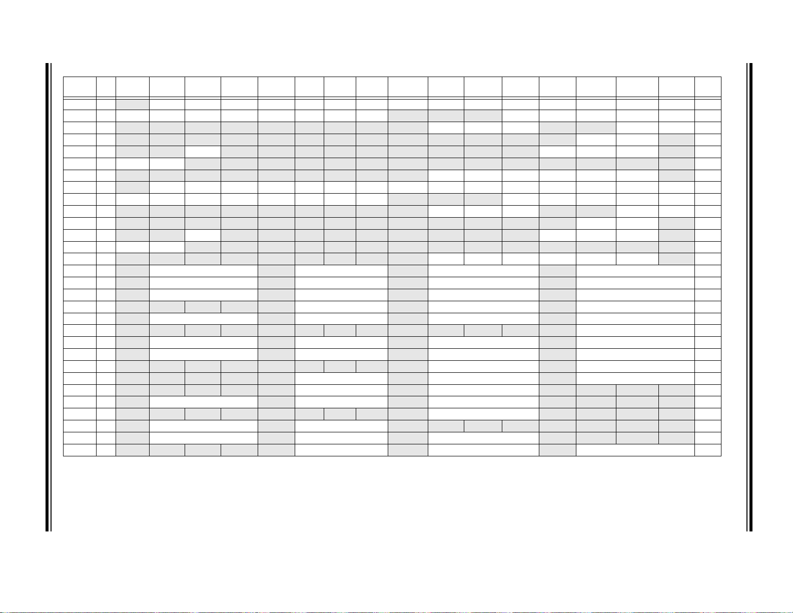
DS70657E-page 64 Preliminary © 2011-2012 Microchip Technology Inc.
TABLE 4-3: INTERRUPT CONTROLLER REGISTER MAP FOR PIC24EPXXXGP20X DEVICES ONLY
File
Addr. Bit 15 Bit 14 Bit 13 Bit 12 Bit 11 Bit 10 Bit 9 Bit 8 Bit 7 Bit 6 Bit 5 Bit 4 Bit 3 Bit 2 Bit 1 Bit 0 All
Name
IFS0 0800 — DMA1IF AD1IF U1TXIF U1RXIF SPI1IF SPI1EIF T3IF T2IF OC2IF IC2IF DMA0IF T1IF OC1IF IC1IF INT0IF
IFS1 0802 U2TXIF U2RXIF INT2IF T5IF T4IF OC4IF OC3IF DMA2IF — — — INT1IF CNIF CMIF MI2C1IF SI2C1IF
IFS2 0804 — — — — — — — — — IC4IF IC3IF DMA3IF — —SPI2IFSPI2EIF
IFS3 0806 — — — — — — — — — — — — — MI2C2IF SI2C2IF —
IFS4 0808 — —CTMUIF— — — — — — — — — CRCIF U2EIF U1EIF —
IFS8 0810 JTAGIF ICDIF — — — — — — — — — — — — — —
IFS9 0812
IEC0 0820
IEC1 0822 U2TXIE U2RXIE INT2IE T5IE T4IE OC4IE OC3IE DMA2IE — — — INT1IE CNIE CMIE MI2C1IE SI2C1IE
IEC2 0824 — — — — — — — — — IC4IE IC3IE DMA3IE — — SPI2IE SPI2EIE
IEC3 0826 — — — — — — — — — — — — — MI2C2IE SI2C2IE —
IEC4 0828 — —CTMUIE — — — — — — — — — CRCIE U2EIE U1EIE —
IEC8 0830 JTAGIE ICDIE — — — — — — — — — — — — — —
IEC9 0832
IPC0 0840
IPC1 0842 — T2IP<2:0> —OC2IP<2:0> — IC2IP<2:0> — DMA0IP<2:0>
IPC2 0844 — U1RXIP<2:0> — SPI1IP<2:0> —SPI1EIP<2:0>— T3IP<2:0>
IPC3 0846 — — — — — DMA1IP<2:0> — AD1IP<2:0> — U1TXIP<2:0>
IPC4 0848 — CNIP<2:0> —CMIP<2:0> — MI2C1IP<2:0> — SI2C1IP<2:0>
IPC5 084A — — — — — — — — — — — — — INT1IP<2:0>
IPC6 084C — T4IP<2:0> —OC4IP<2:0> — OC3IP<2:0> — DMA2IP<2:0>
IPC7 084E — U2TXIP<2:0> — U2RXIP<2:0> — INT2IP<2:0> — T5IP<2:0>
IPC8 0850 — — — — — — — — — SPI2IP<2:0> — SPI2EIP<2:0>
IPC9 0852 — — — — —IC4IP<2:0> — IC3IP<2:0> — DMA3IP<2:0>
IPC12 0858 — — — — — MI2C2IP<2:0> — SI2C2IP<2:0> — — — —
IPC16 0860 — CRCIP<2:0> — U2EIP<2:0> — U1EIP<2:0> — — — —
IPC19 0866 — — — — — — — — —CTMUIP<2:0>— — — —
IPC35 0886 — JTAGID<2:0> — ICDIP<2:0> — — — — — — — —
IPC36 0888 — PTG0IP<2:0> — PGWDTIP<2:0> — PTGSTEPIP<2:0> — — — —
IPC37 088A — — — — — PTG3IP<2:0> — PTG2IP<2:0> — PTG1IP<2:0>
Legend: — = unimplemented, read as ‘0’. Reset values are shown in hexadecimal.
— — — — — — — — — PTG3IF PTG2IF PTG1IF PTG0IF PTGWDTIF PTGSTEPIF —
— DMA1IE AD1IE U1TXIE U1RXIE SPI1IE SPI1EIE T3IE T2IE OC2IE IC2IE DMA0IE T1IE OC1IE IC1IE INT0IE
— — — — — — — — — PTG3IE PTG2IE PTG1IE PTG0IE PTGWDTIE PTGSTEPIE —
— T1IP<2:0> —OC1IP<2:0> — IC1IP<2:0> — INT0IP<2:0>
Resets
0000
0000
0000
0000
0000
0000
0000
0000
0000
0000
0000
0000
0000
0000
4444
4444
4444
0444
4444
0004
4444
4444
0044
0444
0440
4440
0040
4400
4440
0444
dsPIC33EPXXXGP50X, dsPIC33EPXXXMC20X/50X, AND PIC24EPXXXGP/MC20X

© 2011-2012 Microchip Technology Inc. Preliminary DS70657E-page 65
TABLE 4-3: INTERRUPT CONTROLLER REGISTER MAP FOR PIC24EPXXXGP20X DEVICES ONLY (CONTINUED)
File
Addr. Bit 15 Bit 14 Bit 13 Bit 12 Bit 11 Bit 10 Bit 9 Bit 8 Bit 7 Bit 6 Bit 5 Bit 4 Bit 3 Bit 2 Bit 1 Bit 0 All
Name
INTCON1 08C0 NSTDIS OVAERR OVBERR — — — — — — DIV0ERR DMACERR MATHERR ADDRERR STKERR OSCFAIL —
INTCON2 08C2 GIE DISI SWTRAP — — — — — — — — — — INT2EP INT1EP INT0EP
INTCON3 08C4 — — — — — — — — — —DAEDOOVR— — — —
INTCON4 08C6
INTTREG 08C8
Legend: — = unimplemented, read as ‘0’. Reset values are shown in hexadecimal.
— — — — — — — — — — — — — — —SGHT
— — — — ILR<3:0> VECNUM<7:0>
dsPIC33EPXXXGP50X, dsPIC33EPXXXMC20X/50X, AND PIC24EPXXXGP/MC20X
Resets
0000
8000
0000
0000
0000
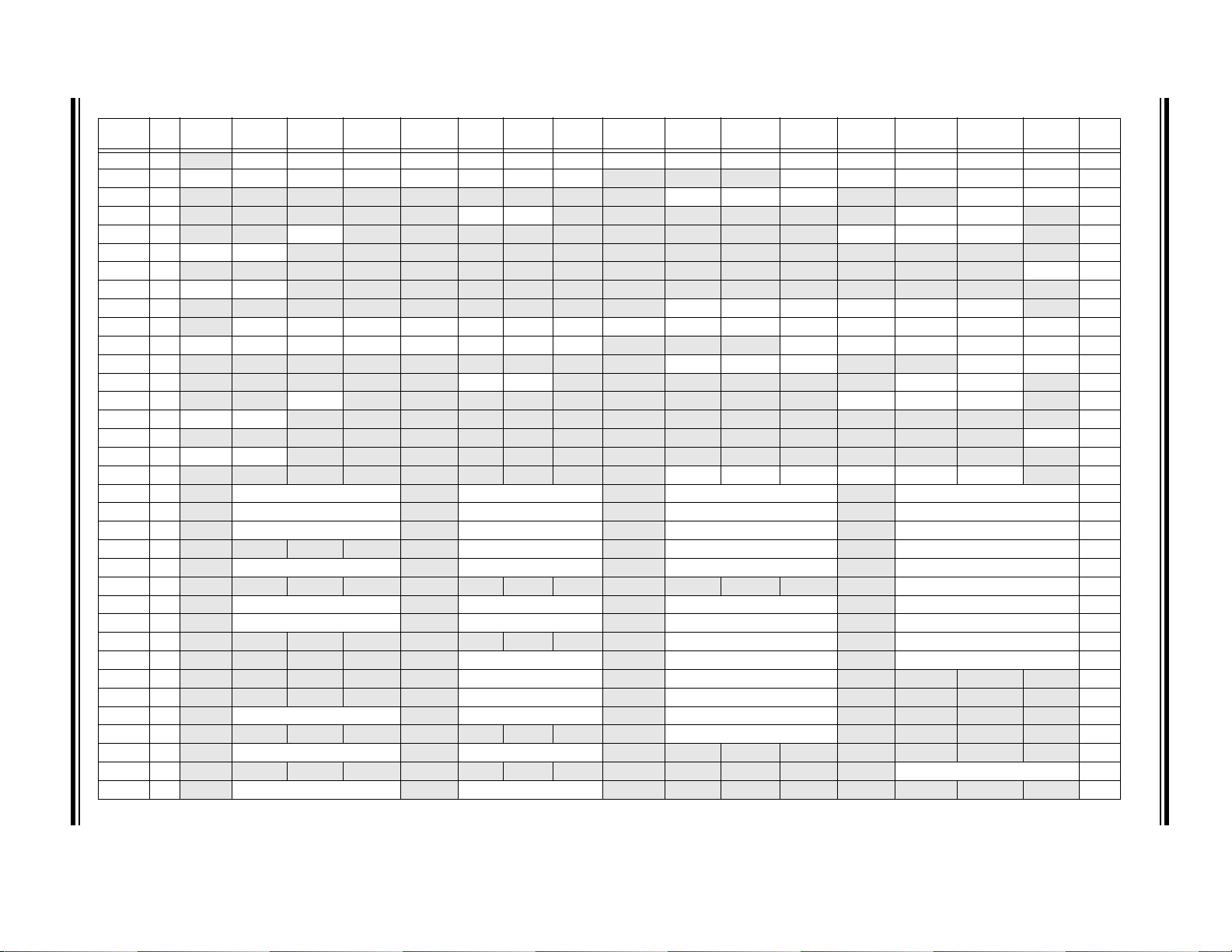
DS70657E-page 66 Preliminary © 2011-2012 Microchip Technology Inc.
TABLE 4-4: INTERRUPT CONTROLLER REGISTER MAP FOR PIC24EPXXXMC20X DEVICES ONLY
File
Addr. Bit 15 Bit 14 Bit 13 Bit 12 Bit 11 Bit 10 Bit 9 Bit 8 Bit 7 Bit 6 Bit 5 Bit 4 Bit 3 Bit 2 Bit 1 Bit 0 All
Name
IFS0 0800 — DMA1IF AD1IF U1TXIF U1RXIF SPI1IF SPI1EIF T3IF T2IF OC2IF IC2IF DMA0IF T1IF OC1IF IC1IF INT0IF
IFS1 0802 U2TXIF U2RXIF INT2IF T5IF T4IF OC4IF OC3IF DMA2IF — — — INT1IF CNIF CMIF MI2C1IF SI2C1IF
IFS2 0804 — — — — — — — — — IC4IF IC3IF DMA3IF — —SPI2IFSPI2EIF
IFS3 0806 — — — — — QEI1IF PSEMIF — — — — — — MI2C2IF SI2C2IF —
IFS4 0808 — —CTMUIF— — — — — — — — — CRCIF U2EIF U1EIF —
IFS5 080A PWM2IF PWM1IF — — — — — — — — — — — — — —
IFS6 080C — — — — — — — — — — — — — — —PWM3IF
IFS8 0810 JTAGIF ICDIF — — — — — — — — — — — — — —
IFS9 0812
IEC0 0820
IEC1 0822 U2TXIE U2RXIE INT2IE T5IE T4IE OC4IE OC3IE DMA2IE — — — INT1IE CNIE CMIE MI2C1IE SI2C1IE
IEC2 0824 — — — — — — — — — IC4IE IC3IE DMA3IE — — SPI2IE SPI2EIE
IEC3 0826 — — — — — QEI1IE PSEMIE — — — — — — MI2C2IE SI2C2IE —
IEC4 0828 — —CTMUIE — — — — — — — — — CRCIE U2EIE U1EIE —
IEC5 082A PWM2IE PWM1IE — — — — — — — — — — — — — —
IEC6 082C — — — — — — — — — — — — — — —PWM3IE
IEC8 0830 JTAGIE ICDIE — — — — — — — — — — — — — —
IEC9 0832
IPC0 0840
IPC1 0842 — T2IP<2:0> —OC2IP<2:0> — IC2IP<2:0> — DMA0IP<2:0>
IPC2 0844 — U1RXIP<2:0> — SPI1IP<2:0> —SPI1EIP<2:0>— T3IP<2:0>
IPC3 0846 — — — — — DMA1IP<2:0> — AD1IP<2:0> — U1TXIP<2:0>
IPC4 0848 — CNIP<2:0> —CMIP<2:0> — MI2C1IP<2:0> — SI2C1IP<2:0>
IPC5 084A — — — — — — — — — — — — — INT1IP<2:0>
IPC6 084C — T4IP<2:0> —OC4IP<2:0> — OC3IP<2:0> — DMA2IP<2:0>
IPC7 084E — U2TXIP<2:0> — U2RXIP<2:0> — INT2IP<2:0> — T5IP<2:0>
IPC8 0850 — — — — — — — — — SPI2IP<2:0> — SPI2EIP<2:0>
IPC9 0852 — — — — —IC4IP<2:0> — IC3IP<2:0> — DMA3IP<2:0>
IPC12 0858 — — — — — MI2C2IP<2:0> — SI2C2IP<2:0> — — — —
IPC14 085C — — — — — QEI1IP<2:0> — PSEMIP<2:0> — — — —
IPC16 0860 — CRCIP<2:0> — U2EIP<2:0> — U1EIP<2:0> — — — —
IPC19 0866 — — — — — — — — —CTMUIP<2:0>— — — —
IPC23 086E — PWM2IP<2:0> — PWM1IP<2:0> — — — — — — — —
IPC24 0870 — — — — — — — — — — — — — PWM3IP<2:0>
IPC35 0886 — JTAGID<2:0> — ICDIP<2:0> — — — — — — — —
Legend: — = unimplemented, read as ‘0’. Reset values are shown in hexadecimal.
— — — — — — — — — PTG3IF PTG2IF PTG1IF PTG0IF PTGWDTIF PTGSTEPIF —
— DMA1IE AD1IE U1TXIE U1RXIE SPI1IE SPI1EIE T3IE T2IE OC2IE IC2IE DMA0IE T1IE OC1IE IC1IE INT0IE
— — — — — — — — — PTG3IE PTG2IE PTG1IE PTG0IE PTGWDTIE PTGSTEPIE —
— T1IP<2:0> —OC1IP<2:0> — IC1IP<2:0> — INT0IP<2:0>
Resets
0000
0000
0000
0000
0000
0000
0000
0000
0000
0000
0000
0000
0000
0000
0000
0000
0000
0000
4444
4444
4444
0444
4444
0004
4444
4444
0044
0444
0440
0440
4440
0040
4400
4004
4400
dsPIC33EPXXXGP50X, dsPIC33EPXXXMC20X/50X, AND PIC24EPXXXGP/MC20X
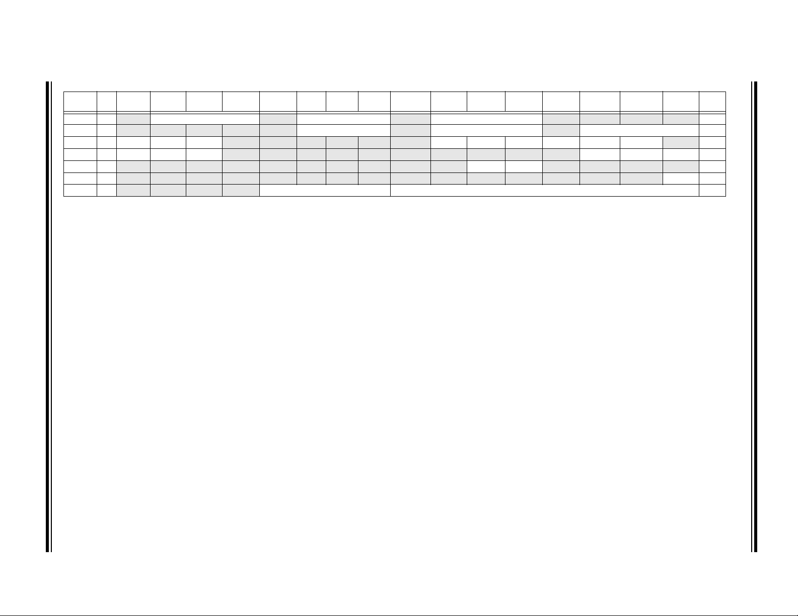
© 2011-2012 Microchip Technology Inc. Preliminary DS70657E-page 67
TABLE 4-4: INTERRUPT CONTROLLER REGISTER MAP FOR PIC24EPXXXMC20X DEVICES ONLY (CONTINUED)
File
Addr. Bit 15 Bit 14 Bit 13 Bit 12 Bit 11 Bit 10 Bit 9 Bit 8 Bit 7 Bit 6 Bit 5 Bit 4 Bit 3 Bit 2 Bit 1 Bit 0 All
Name
IPC36 0888 — PTG0IP<2:0> — PGWDTIP<2:0> — PTGSTEPIP<2:0> — — — —
IPC37 088A — — — — — PTG3IP<2:0> — PTG2IP<2:0> — PTG1IP<2:0>
INTCON1 08C0 NSTDIS OVAERR OVBERR — — — — — — DIV0ERR DMACERR MATHERR ADDRERR STKERR OSCFAIL —
INTCON2 08C2 GIE DISI SWTRAP — — — — — — — — — — INT2EP INT1EP INT0EP
INTCON3 08C4 — — — — — — — — — —DAEDOOVR— — — —
INTCON4 08C6
INTTREG 08C8
Legend: — = unimplemented, read as ‘0’. Reset values are shown in hexadecimal.
— — — — — — — — — — — — — — —SGHT
— — — — ILR<3:0> VECNUM<7:0>
dsPIC33EPXXXGP50X, dsPIC33EPXXXMC20X/50X, AND PIC24EPXXXGP/MC20X
Resets
4440
0444
0000
8000
0000
0000
0000

DS70657E-page 68 Preliminary © 2011-2012 Microchip Technology Inc.
TABLE 4-5: INTERRUPT CONTROLLER REGISTER MAP FOR dsPIC33EPXXXGP50X DEVICES ONLY
File
Addr. Bit 15 Bit 14 Bit 13 Bit 12 Bit 11 Bit 10 Bit 9 Bit 8 Bit 7 Bit 6 Bit 5 Bit 4 Bit 3 Bit 2 Bit 1 Bit 0 All
Name
IFS0 0800 — DMA1IF AD1IF U1TXIF U1RXIF SPI1IF SPI1EIF T3IF T2IF OC2IF IC2IF DMA0IF T1IF OC1IF IC1IF INT0IF
IFS1 0802 U2TXIF U2RXIF INT2IF T5IF T4IF OC4IF OC3IF DMA2IF — — — INT1IF CNIF CMIF MI2C1IF SI2C1IF
IFS2 0804 — — — — — — — — — IC4IF IC3IF DMA3IF C1IF C1RXIF SPI2IF SPI2EIF
IFS3 0806 — — — — — — — — — — — — — MI2C2IF SI2C2IF —
IFS4 0808 — —CTMUIF— — — — — —C1TXIF— — CRCIF U2EIF U1EIF —
IFS6 080C — — — — — — — — — — — — — — —PWM3IF
IFS8 0810 JTAGIF ICDIF — — — — — — — — — — — — — —
IFS9 0812
IEC0 0820
IEC1 0822 U2TXIE U2RXIE INT2IE T5IE T4IE OC4IE OC3IE DMA2IE — — — INT1IE CNIE CMIE MI2C1IE SI2C1IE
IEC2 0824 — — — — — — — — — IC4IE IC3IE DMA3IE C1IE C1RXIE SPI2IE SPI2EIE
IEC3 0826 — — — — — — — — — — — — — MI2C2IE SI2C2IE —
IEC4 0828 — —CTMUIE — — — — — —C1TXIE— — CRCIE U2EIE U1EIE —
IEC8 0830 JTAGIE ICDIE — — — — — — — — — — — — — —
IEC9 0832
IPC0 0840
IPC1 0842 — T2IP<2:0> —OC2IP<2:0> — IC2IP<2:0> — DMA0IP<2:0>
IPC2 0844 — U1RXIP<2:0> — SPI1IP<2:0> —SPI1EIP<2:0>— T3IP<2:0>
IPC3 0846 — — — — — DMA1IP<2:0> — AD1IP<2:0> — U1TXIP<2:0>
IPC4 0848 — CNIP<2:0> —CMIP<2:0> — MI2C1IP<2:0> — SI2C1IP<2:0>
IPC5 084A — — — — — — — — — — — — — INT1IP<2:0>
IPC6 084C — T4IP<2:0> —OC4IP<2:0> — OC3IP<2:0> — DMA2IP<2:0>
IPC7 084E — U2TXIP<2:0> — U2RXIP<2:0> — INT2IP<2:0> — T5IP<2:0>
IPC8 0850 — C1IP<2:0> — C1RXIP<2:0> — SPI2IP<2:0> — SPI2EIP<2:0>
IPC9 0852 — — — — —IC4IP<2:0> — IC3IP<2:0> — DMA3IP<2:0>
IPC11 0856 — — — — — — — — — — — — — — — —
IPC12 0858 — — — — — MI2C2IP<2:0> — SI2C2IP<2:0> — — — —
IPC16 0860 — CRCIP<2:0> — U2EIP<2:0> — U1EIP<2:0> — — — —
IPC17 0862 — — — — — C1TXIP<2:0> — — — — — — — —
IPC19 0866 — — — — — — — — —CTMUIP<2:0>— — — —
IPC35 0886 — JTAGID<2:0> — ICDIP<2:0> — — — — — — — —
IPC36 0888 — PTG0IP<2:0> — PGWDTIP<2:0> — PTGSTEPIP<2:0> — — — —
IPC37 088A — — — — — PTG3IP<2:0> — PTG2IP<2:0> — PTG1IP<2:0>
Legend: — = unimplemented, read as ‘0’. Reset values are shown in hexadecimal.
— — — — — — — — — PTG3IF PTG2IF PTG1IF PTG0IF PTGWDTIF PTGSTEPIF —
— DMA1IE AD1IE U1TXIE U1RXIE SPI1IE SPI1EIE T3IE T2IE OC2IE IC2IE DMA0IE T1IE OC1IE IC1IE INT0IE
— — — — — — — — — PTG3IE PTG2IE PTG1IE PTG0IE PTGWDTIE PTGSTEPIE —
— T1IP<2:0> —OC1IP<2:0> — IC1IP<2:0> — INT0IP<2:0>
Resets
0000
0000
0000
0000
0000
0000
0000
0000
0000
0000
0000
0000
0000
0000
0000
4444
4444
4444
0444
4444
0004
4444
4444
4444
0444
0000
0440
4440
0400
0040
4400
4440
0444
dsPIC33EPXXXGP50X, dsPIC33EPXXXMC20X/50X, AND PIC24EPXXXGP/MC20X
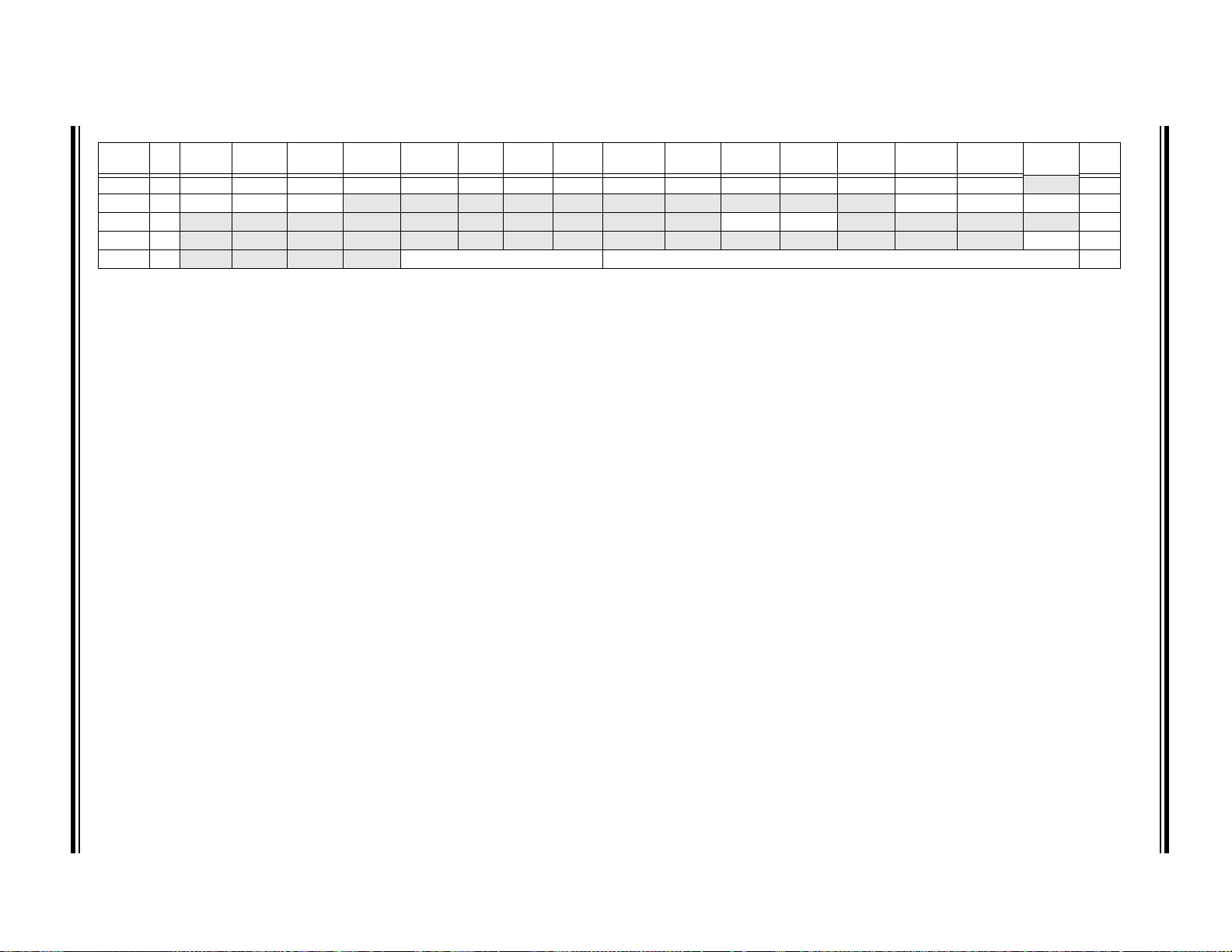
© 2011-2012 Microchip Technology Inc. Preliminary DS70657E-page 69
TABLE 4-5: INTERRUPT CONTROLLER REGISTER MAP FOR dsPIC33EPXXXGP50X DEVICES ONLY (CONTINUED)
File
Addr. Bit 15 Bit 14 Bit 13 Bit 12 Bit 11 Bit 10 Bit 9 Bit 8 Bit 7 Bit 6 Bit 5 Bit 4 Bit 3 Bit 2 Bit 1 Bit 0 All
Name
INTCON1 08C0 NSTDIS OVAERR OVBERR COVAERR COVBERR OVATE OVBTE COVTE SFTACERR DIV0ERR DMACERR MATHERR ADDRERR STKERR OSCFAIL —
INTCON2 08C2 GIE DISI SWTRAP — — — — — — — — — — INT2EP INT1EP INT0EP
INTCON3 08C4 — — — — — — — — — —DAEDOOVR— — — —
INTCON4 08C6
INTTREG 08C8
Legend: — = unimplemented, read as ‘0’. Reset values are shown in hexadecimal.
— — — — — — — — — — — — — — —SGHT
— — — — ILR<3:0> VECNUM<7:0>
dsPIC33EPXXXGP50X, dsPIC33EPXXXMC20X/50X, AND PIC24EPXXXGP/MC20X
Resets
0000
8000
0000
0000
0000
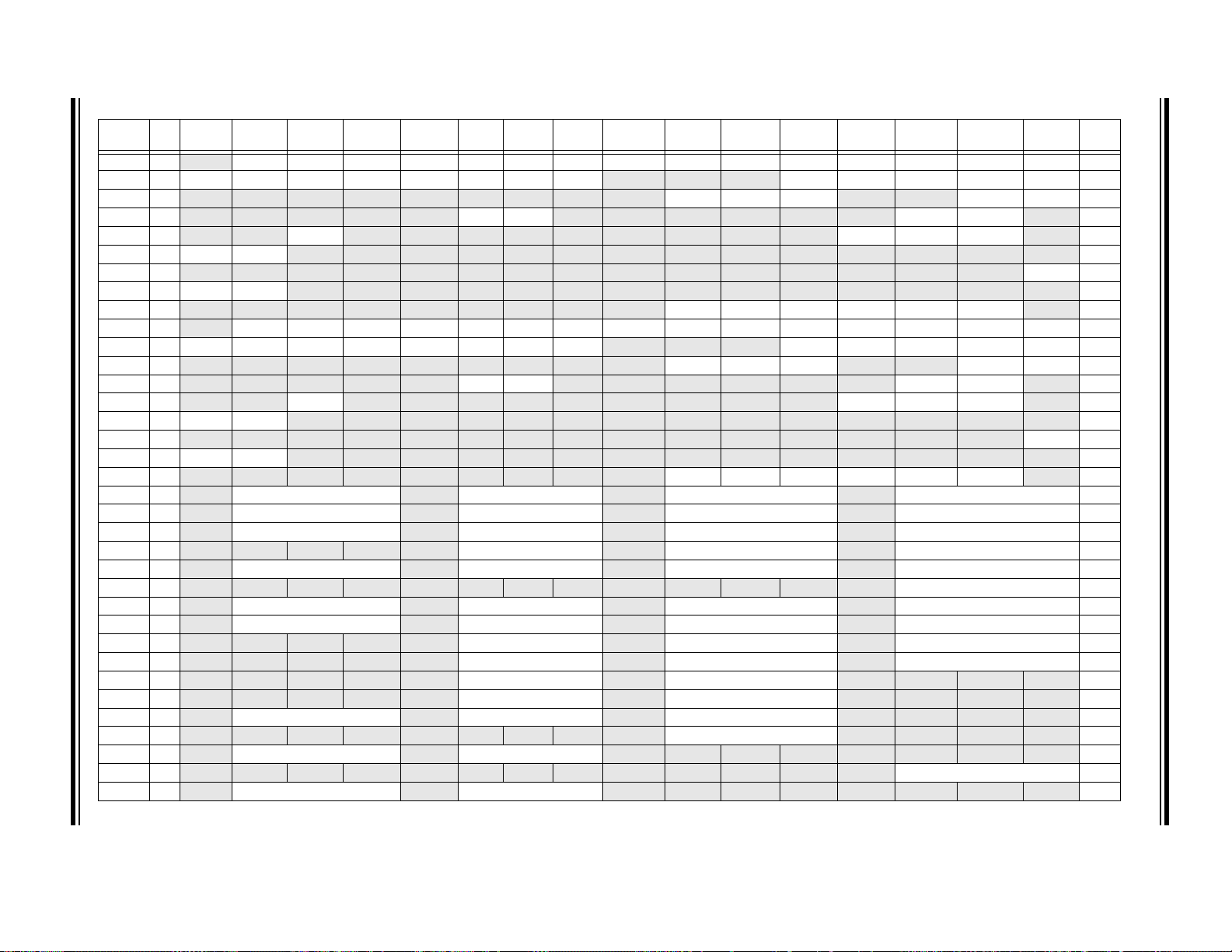
DS70657E-page 70 Preliminary © 2011-2012 Microchip Technology Inc.
TABLE 4-6: INTERRUPT CONTROLLER REGISTER MAP FOR dsPIC33EPXXXMC20X DEVICES ONLY
File
Addr. Bit 15 Bit 14 Bit 13 Bit 12 Bit 11 Bit 10 Bit 9 Bit 8 Bit 7 Bit 6 Bit 5 Bit 4 Bit 3 Bit 2 Bit 1 Bit 0 All
Name
IFS0 0800 — DMA1IF AD1IF U1TXIF U1RXIF SPI1IF SPI1EIF T3IF T2IF OC2IF IC2IF DMA0IF T1IF OC1IF IC1IF INT0IF
IFS1 0802 U2TXIF U2RXIF INT2IF T5IF T4IF OC4IF OC3IF DMA2IF — — — INT1IF CNIF CMIF MI2C1IF SI2C1IF
IFS2 0804 — — — — — — — — — IC4IF IC3IF DMA3IF — —SPI2IFSPI2EIF
IFS3 0806 — — — — — QEI1IF PSEMIF — — — — — — MI2C2IF SI2C2IF —
IFS4 0808 — —CTMUIF— — — — — — — — — CRCIF U2EIF U1EIF —
IFS5 080A PWM2IF PWM1IF — — — — — — — — — — — — — —
IFS6 080C — — — — — — — — — — — — — — —PWM3IF
IFS8 0810 JTAGIF ICDIF — — — — — — — — — — — — — —
IFS9 0812
IEC0 0820
IEC1 0822 U2TXIE U2RXIE INT2IE T5IE T4IE OC4IE OC3IE DMA2IE — — — INT1IE CNIE CMIE MI2C1IE SI2C1IE
IEC2 0824 — — — — — — — — — IC4IE IC3IE DMA3IE — — SPI2IE SPI2EIE
IEC3 0826 — — — — — QEI1IE PSEMIE — — — — — — MI2C2IE SI2C2IE —
IEC4 0828 — —CTMUIE — — — — — — — — — CRCIE U2EIE U1EIE —
IEC5 082A PWM2IE PWM1IE — — — — — — — — — — — — — —
IEC6 082C — — — — — — — — — — — — — — —PWM3IE
IEC8 0830 JTAGIE ICDIE — — — — — — — — — — — — — —
IEC9 0832
IPC0 0840
IPC1 0842 — T2IP<2:0> —OC2IP<2:0> — IC2IP<2:0> — DMA0IP<2:0>
IPC2 0844 — U1RXIP<2:0> — SPI1IP<2:0> —SPI1EIP<2:0>— T3IP<2:0>
IPC3 0846 — — — — — DMA1IP<2:0> — AD1IP<2:0> — U1TXIP<2:0>
IPC4 0848 — CNIP<2:0> —CMIP<2:0> — MI2C1IP<2:0> — SI2C1IP<2:0>
IPC5 084A — — — — — — — — — — — — — INT1IP<2:0>
IPC6 084C — T4IP<2:0> —OC4IP<2:0> — OC3IP<2:0> — DMA2IP<2:0>
IPC7 084E — U2TXIP<2:0> — U2RXIP<2:0> — INT2IP<2:0> — T5IP<2:0>
IPC8 0850 — — — — — C1RXIP<2:0> — SPI2IP<2:0> — SPI2EIP<2:0>
IPC9 0852 — — — — —IC4IP<2:0> — IC3IP<2:0> — DMA3IP<2:0>
IPC12 0858 — — — — — MI2C2IP<2:0> — SI2C2IP<2:0> — — — —
IPC14 085C — — — — — QEI1IP<2:0> — PSEMIP<2:0> — — — —
IPC16 0860 — CRCIP<2:0> — U2EIP<2:0> — U1EIP<2:0> — — — —
IPC19 0866 — — — — — — — — —CTMUIP<2:0>— — — —
IPC23 086E — PWM2IP<2:0> — PWM1IP<2:0> — — — — — — — —
IPC24 0870 — — — — — — — — — — — — — PWM3IP<2:0>
IPC35 0886 — JTAGID<2:0> — ICDIP<2:0> — — — — — — — —
Legend: — = unimplemented, read as ‘0’. Reset values are shown in hexadecimal.
— — — — — — — — — PTG3IF PTG2IF PTG1IF PTG0IF PTGWDTIF PTGSTEPIF —
— DMA1IE AD1IE U1TXIE U1RXIE SPI1IE SPI1EIE T3IE T2IE OC2IE IC2IE DMA0IE T1IE OC1IE IC1IE INT0IE
— — — — — — — — — PTG3IE PTG2IE PTG1IE PTG0IE PTGWDTIE PTGSTEPIE —
— T1IP<2:0> —OC1IP<2:0> — IC1IP<2:0> — INT0IP<2:0>
Resets
0000
0000
0000
0000
0000
0000
0000
0000
0000
0000
0000
0000
0000
0000
0000
0000
0000
0000
4444
4444
4444
0444
4444
0004
4444
4444
0444
0444
0440
0440
4440
0040
4400
0004
4400
dsPIC33EPXXXGP50X, dsPIC33EPXXXMC20X/50X, AND PIC24EPXXXGP/MC20X
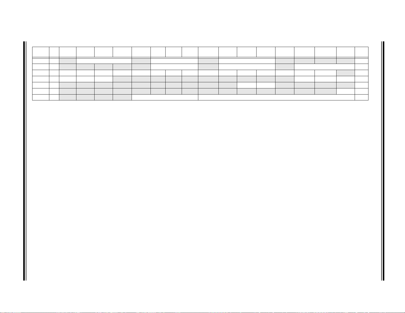
© 2011-2012 Microchip Technology Inc. Preliminary DS70657E-page 71
TABLE 4-6: INTERRUPT CONTROLLER REGISTER MAP FOR dsPIC33EPXXXMC20X DEVICES ONLY (CONTINUED)
File
Addr. Bit 15 Bit 14 Bit 13 Bit 12 Bit 11 Bit 10 Bit 9 Bit 8 Bit 7 Bit 6 Bit 5 Bit 4 Bit 3 Bit 2 Bit 1 Bit 0 All
Name
IPC36 0888 — PTG0IP<2:0> — PGWDTIP<2:0> — PTGSTEPIP<2:0> — — — —
IPC37 088A — — — — — PTG3IP<2:0> — PTG2IP<2:0> — PTG1IP<2:0>
INTCON1 08C0 NSTDIS OVAERR OVBERR COVAERR COVBERR OVATE OVBTE COVTE SFTACERR DIV0ERR DMACERR MATHERR ADDRERR STKERR OSCFAIL —
INTCON2 08C2 GIE DISI SWTRAP — — — — — — — — — — INT2EP INT1EP INT0EP
INTCON3 08C4 — — — — — — — — — —DAEDOOVR— — — —
INTCON4 08C6
INTTREG 08C8
Legend: — = unimplemented, read as ‘0’. Reset values are shown in hexadecimal.
— — — — — — — — — — — — — — —SGHT
— — — — ILR<3:0> VECNUM<7:0>
dsPIC33EPXXXGP50X, dsPIC33EPXXXMC20X/50X, AND PIC24EPXXXGP/MC20X
Resets
4440
0444
0000
8000
0000
0000
0000
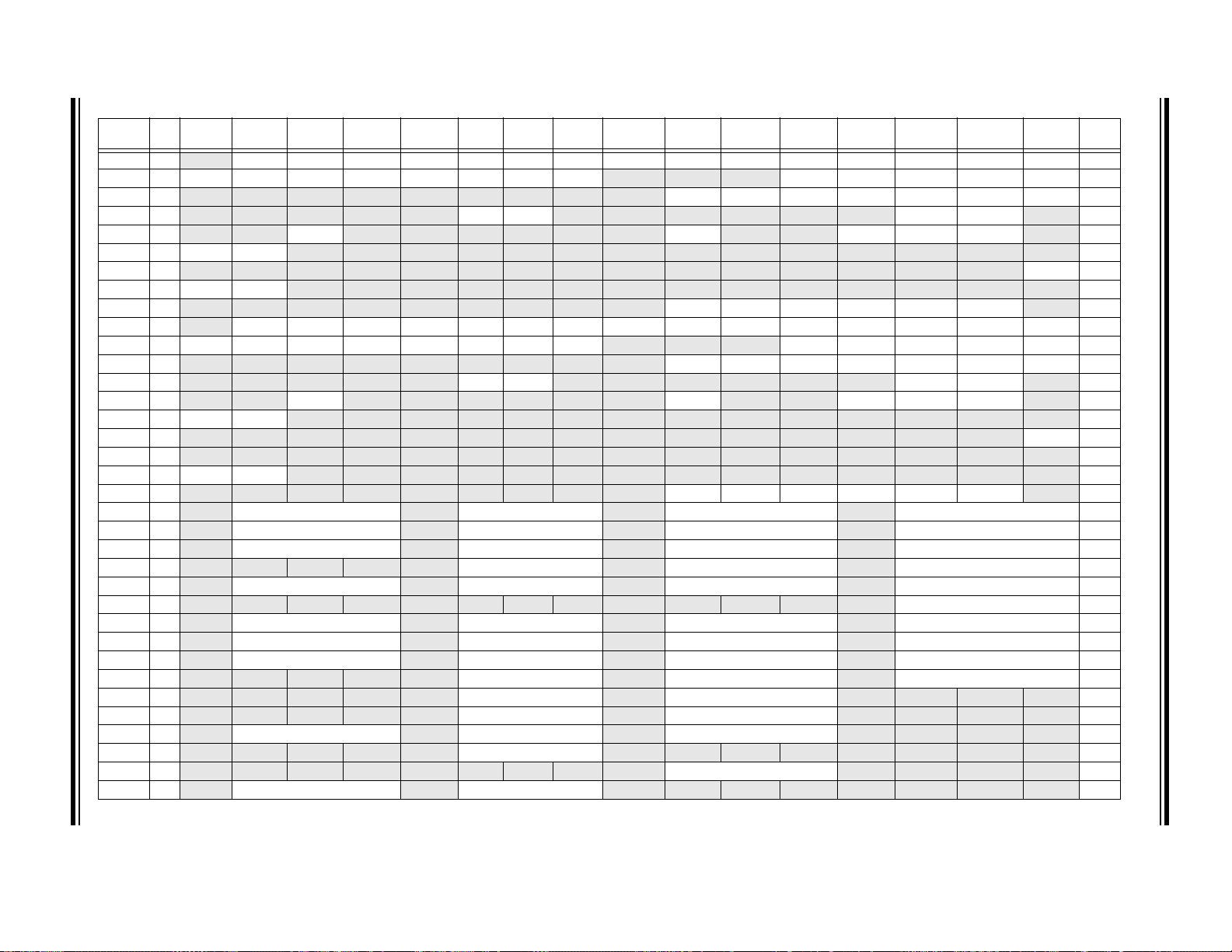
DS70657E-page 72 Preliminary © 2011-2012 Microchip Technology Inc.
TABLE 4-7: INTERRUPT CONTROLLER REGISTER MAP FOR dsPIC33EPXXXMC50X DEVICES ONLY
File
Addr. Bit 15 Bit 14 Bit 13 Bit 12 Bit 11 Bit 10 Bit 9 Bit 8 Bit 7 Bit 6 Bit 5 Bit 4 Bit 3 Bit 2 Bit 1 Bit 0 All
Name
IFS0 0800 — DMA1IF AD1IF U1TXIF U1RXIF SPI1IF SPI1EIF T3IF T2IF OC2IF IC2IF DMA0IF T1IF OC1IF IC1IF INT0IF
IFS1 0802 U2TXIF U2RXIF INT2IF T5IF T4IF OC4IF OC3IF DMA2IF — — — INT1IF CNIF CMIF MI2C1IF SI2C1IF
IFS2 0804 — — — — — — — — — IC4IF IC3IF DMA3IF C1IF C1RXIF SPI2IF SPI2EIF
IFS3 0806 — — — — — QEI1IF PSEMIF — — — — — — MI2C2IF SI2C2IF —
IFS4 0808 — —CTMUIF— — — — — —C1TXIF— — CRCIF U2EIF U1EIF —
IFS5 080A PWM2IF PWM1IF — — — — — — — — — — — — — —
IFS6 080C — — — — — — — — — — — — — — —PWM3IF
IFS8 0810 JTAGIF ICDIF — — — — — — — — — — — — — —
IFS9 0812
IEC0 0820
IEC1 0822 U2TXIE U2RXIE INT2IE T5IE T4IE OC4IE OC3IE DMA2IE — — — INT1IE CNIE CMIE MI2C1IE SI2C1IE
IEC2 0824 — — — — — — — — — IC4IE IC3IE DMA3IE C1IE C1RXIE SPI2IE SPI2EIE
IEC3 0826 — — — — — QEI1IE PSEMIE — — — — — — MI2C2IE SI2C2IE —
IEC4 0828 — —CTMUIE — — — — — —C1TXIE— — CRCIE U2EIE U1EIE —
IEC5 082A PWM2IE PWM1IE — — — — — — — — — — — — — —
IEC6 082C — — — — — — — — — — — — — — —PWM3IE
IEC7 082E — — — — — — — — — — — — — — — —
IEC8 0830 JTAGIE ICDIE — — — — — — — — — — — — — —
IEC9 0832
IPC0 0840
IPC1 0842 — T2IP<2:0> —OC2IP<2:0> — IC2IP<2:0> — DMA0IP<2:0>
IPC2 0844 — U1RXIP<2:0> — SPI1IP<2:0> —SPI1EIP<2:0>— T3IP<2:0>
IPC3 0846 — — — — — DMA1IP<2:0> — AD1IP<2:0> — U1TXIP<2:0>
IPC4 0848 — CNIP<2:0> —CMIP<2:0> — MI2C1IP<2:0> — SI2C1IP<2:0>
IPC5 084A — — — — — — — — — — — — — INT1IP<2:0>
IPC6 084C — T4IP<2:0> —OC4IP<2:0> — OC3IP<2:0> — DMA2IP<2:0>
IPC7 084E — U2TXIP<2:0> — U2RXIP<2:0> — INT2IP<2:0> — T5IP<2:0>
IPC8 0850 — C1IP<2:0> — C1RXIP<2:0> — SPI2IP<2:0> — SPI2EIP<2:0>
IPC9 0852 — — — — —IC4IP<2:0> — IC3IP<2:0> — DMA3IP<2:0>
IPC12 0858 — — — — — MI2C2IP<2:0> — SI2C2IP<2:0> — — — —
IPC14 085C — — — — — QEI1IP<2:0> — PSEMIP<2:0> — — — —
IPC16 0860 — CRCIP<2:0> — U2EIP<2:0> — U1EIP<2:0> — — — —
IPC17 0862 — — — — — C1TXIP<2:0> — — — — — — — —
IPC19 0866 — — — — — — — — —CTMUIP<2:0>— — — —
IPC23 086E — PWM2IP<2:0> — PWM1IP<2:0> — — — — — — — —
Legend: — = unimplemented, read as ‘0’. Reset values are shown in hexadecimal.
— — — — — — — — — PTG3IF PTG2IF PTG1IF PTG0IF PTGWDTIF PTGSTEPIF —
— DMA1IE AD1IE U1TXIE U1RXIE SPI1IE SPI1EIE T3IE T2IE OC2IE IC2IE DMA0IE T1IE OC1IE IC1IE INT0IE
— — — — — — — — — PTG3IE PTG2IE PTG1IE PTG0IE PTGWDTIE PTGSTEPIE —
— T1IP<2:0> —OC1IP<2:0> — IC1IP<2:0> — INT0IP<2:0>
Resets
0000
0000
0000
0000
0000
0000
0000
0000
0000
0000
0000
0000
0000
0000
0000
0000
0000
0000
0000
4444
4444
4444
0444
4444
0004
4444
4444
4444
0444
0440
0440
4440
0400
0040
4400
dsPIC33EPXXXGP50X, dsPIC33EPXXXMC20X/50X, AND PIC24EPXXXGP/MC20X

© 2011-2012 Microchip Technology Inc. Preliminary DS70657E-page 73
TABLE 4-7: INTERRUPT CONTROLLER REGISTER MAP FOR dsPIC33EPXXXMC50X DEVICES ONLY (CONTINUED)
File
Addr. Bit 15 Bit 14 Bit 13 Bit 12 Bit 11 Bit 10 Bit 9 Bit 8 Bit 7 Bit 6 Bit 5 Bit 4 Bit 3 Bit 2 Bit 1 Bit 0 All
Name
IPC24 0870 — — — — — — — — — — — — — PWM3IP<2:0>
IPC35 0886 — JTAGID<2:0> — ICDIP<2:0> — — — — — — — —
IPC36 0888 — PTG0IP<2:0> — PGWDTIP<2:0> — PTGSTEPIP<2:0> — — — —
IPC37 088A — — — — — PTG3IP<2:0> — PTG2IP<2:0> — PTG1IP<2:0>
INTCON1 08C0 NSTDIS OVAERR OVBERR COVAERR COVBERR OVATE OVBTE COVTE SFTACERR DIV0ERR DMACERR MATHERR ADDRERR STKERR OSCFAIL —
INTCON2 08C2 GIE DISI SWTRAP — — — — — — — — — — INT2EP INT1EP INT0EP
INTCON3 08C4 — — — — — — — — — —DAEDOOVR— — — —
INTCON4 08C6
INTTREG 08C8
Legend: — = unimplemented, read as ‘0’. Reset values are shown in hexadecimal.
— — — — — — — — — — — — — — —SGHT
— — — — ILR<3:0> VECNUM<7:0>
dsPIC33EPXXXGP50X, dsPIC33EPXXXMC20X/50X, AND PIC24EPXXXGP/MC20X
Resets
0004
4400
4440
0444
0000
8000
0000
0000
0000

DS70657E-page 74 Preliminary © 2011-2012 Microchip Technology Inc.
TABLE 4-8: TIMER1 THROUGH TIMER5 REGISTER MAP
SFR Name Addr. Bit 15 Bit 14 Bit 13 Bit 12 Bit 11 Bit 10 Bit 9 Bit 8 Bit 7 Bit 6 Bit 5 Bit 4 Bit 3 Bit 2 Bit 1 Bit 0
TMR1 0100 Timer1 Register xxxx
PR1 0102 Period Register 1 FFFF
T1CON 0104 TON
TMR2 0106 Timer2 Register xxxx
TMR3HLD 0108 Timer3 Holding Register (for 32-bit timer operations only) xxxx
TMR3 010A Timer3 Register xxxx
PR2 010C Period Register 2 FFFF
PR3 010E Period Register 3 FFFF
T2CON 0110 TON
T3CON 0112 TON
TMR4 0114 Timer4 Register xxxx
TMR5HLD 0116 Timer5 Holding Register (for 32-bit operations only) xxxx
TMR5 0118 Timer5 Register xxxx
PR4 011A Period Register 4 FFFF
PR5 011C Period Register 5 FFFF
T4CON 011E TON
T5CON 0120 TON
Legend: x = unknown value on Reset, — = unimplemented, read as ‘0’. Reset values are shown in hexadecimal.
—TSIDL— — — — — — TGATE TCKPS<1:0> —TSYNCTCS — 0000
—TSIDL— — — — — — TGATE TCKPS<1:0> T32 —TCS— 0000
—TSIDL— — — — — — TGATE TCKPS<1:0> — —TCS— 0000
—TSIDL— — — — — — TGATE TCKPS<1:0> T32 —TCS— 0000
—TSIDL— — — — — — TGATE TCKPS<1:0> — —TCS— 0000
All
Resets
dsPIC33EPXXXGP50X, dsPIC33EPXXXMC20X/50X, AND PIC24EPXXXGP/MC20X

© 2011-2012 Microchip Technology Inc. Preliminary DS70657E-page 75
TABLE 4-9: INPUT CAPTURE 1 THROUGH INPUT CAPTURE 4 REGISTER MAP
File Name Addr. Bit 15 Bit 14 Bit 13 Bit 12 Bit 11 Bit 10 Bit 9 Bit 8 Bit 7 Bit 6 Bit 5 Bit 4 Bit 3 Bit 2 Bit 1 Bit 0
IC1CON1 0140
IC1CON2 0142
IC1BUF
IC1TMR 0146 Input Capture 1 Timer 0000
IC2CON1 0148
IC2CON2 014A
IC2BUF
IC2TMR 014E Input Capture 2 Timer 0000
IC3CON1 0150
IC3CON2 0152
IC3BUF
IC3TMR 0156 Input Capture 3 Timer 0000
IC4CON1 0158
IC4CON2 015A
IC4BUF
IC4TMR 015E Input Capture 4 Timer 0000
Legend: x = unknown value on Reset, — = unimplemented, read as ‘0’. Reset values are shown in hexadecimal.
0144
014C
0154
015C
— — ICSIDL ICTSEL<2:0> — — — ICI<1:0> ICOV ICBNE ICM<2:0> 0000
— — — — — — — IC32 ICTRIG TRIGSTAT — SYNCSEL<4:0> 000D
Input Capture 1 Buffer Register xxxx
— — ICSIDL ICTSEL<2:0> — — — ICI<1:0> ICOV ICBNE ICM<2:0> 0000
— — — — — — — IC32 ICTRIG TRIGSTAT — SYNCSEL<4:0> 000D
Input Capture 2 Buffer Register xxxx
— — ICSIDL ICTSEL<2:0> — — — ICI<1:0> ICOV ICBNE ICM<2:0> 0000
— — — — — — — IC32 ICTRIG TRIGSTAT — SYNCSEL<4:0> 000D
Input Capture 3 Buffer Register xxxx
— — ICSIDL ICTSEL<2:0> — — — ICI<1:0> ICOV ICBNE ICM<2:0> 0000
— — — — — — — IC32 ICTRIG TRIGSTAT — SYNCSEL<4:0> 000D
Input Capture 4 Buffer Register xxxx
All
Resets
dsPIC33EPXXXGP50X, dsPIC33EPXXXMC20X/50X, AND PIC24EPXXXGP/MC20X

DS70657E-page 76 Preliminary © 2011-2012 Microchip Technology Inc.
TABLE 4-10: OUTPUT COMPARE 1 THROUGH OUTPUT COMPARE 4 REGISTER MAP
File Name Addr. Bit 15 Bit 14 Bit 13 Bit 12 Bit 11 Bit 10 Bit 9 Bit 8 Bit 7 Bit 6 Bit 5 Bit 4 Bit 3 Bit 2 Bit 1 Bit 0
OC1CON1
OC1CON2
OC1RS
OC1R
OC1TMR
OC2CON1
OC2CON2
OC2RS
OC2R
OC2TMR
OC3CON1
OC3CON2
OC3RS
OC3R
OC3TMR
OC4CON1
OC4CON2
OC4RS
OC4R
OC4TMR
Legend:
0900
0902
0904
0906
0908
090A
090C
090E
0910
0912
0914
0916
0918
091A
091C
091E
0920
0922
0924
0926
— = unimplemented, read as ‘0’. Reset values are shown in hexadecimal.
— — OCSIDL OCTSEL<2:0> — ENFLTB ENFLTA — OCFLTB OCFLTA TRIGMODE OCM<2:0>
FLTMD FLTOUT FLTTRIEN OCINV — — — OC32 OCTRIG TRIGSTAT OCTRIS SYNCSEL<4:0>
Output Compare 1 Secondary Register
Output Compare 1 Register
Timer Value 1 Register
— — OCSIDL OCTSEL<2:0> — ENFLTB ENFLTA — OCFLTB OCFLTA TRIGMODE OCM<2:0>
FLTMD FLTOUT FLTTRIEN OCINV — — — OC32 OCTRIG TRIGSTAT OCTRIS SYNCSEL<4:0>
Output Compare 2 Secondary Register
Output Compare 2 Register
Timer Value 2 Register
— — OCSIDL OCTSEL<2:0> — ENFLTB ENFLTA — OCFLTB OCFLTA TRIGMODE OCM<2:0>
FLTMD FLTOUT FLTTRIEN OCINV — — — OC32 OCTRIG TRIGSTAT OCTRIS SYNCSEL<4:0>
Output Compare 3 Secondary Register
Output Compare 3 Register
Timer Value 3 Register
— — OCSIDL OCTSEL<2:0> ENFLTC ENFLTB ENFLTA OCFLTC OCFLTB OCFLTA TRIGMODE OCM<2:0>
FLTMD FLTOUT FLTTRIEN OCINV — — — OC32 OCTRIG TRIGSTAT OCTRIS SYNCSEL<4:0>
Output Compare 4 Secondary Register
Output Compare 4 Register
Timer Value 4 Register
dsPIC33EPXXXGP50X, dsPIC33EPXXXMC20X/50X, AND PIC24EPXXXGP/MC20X
All
Resets
0000
000C
xxxx
xxxx
xxxx
0000
000C
xxxx
xxxx
xxxx
0000
000C
xxxx
xxxx
xxxx
0000
000C
xxxx
xxxx
xxxx

© 2011-2012 Microchip Technology Inc. Preliminary DS70657E-page 77
TABLE 4-11: PTG REGISTER MAP
File Name Addr. Bit 15 Bit 14 Bit 13 Bit 12 Bit 11 Bit 10 Bit 9 Bit 8 Bit 7 Bit 6 Bit 5 Bit 4 Bit 3 Bit 2 Bit 1 Bit 0
PTGCST 0AC0 PTGEN
PTGCON 0AC2 PTGCLK<2:0> PTGDIV<4:0> PTGPWD<3:0>
PTGBTE 0AC4 PTGBTE<15:0> 0000
PTGHOLD 0AC6 PTGHOLD<15:0> 0000
PTGT0LIM 0AC8 PTGT0LIM<15:0> 0000
PTGT1LIM 0ACA PTGT1LIM<15:0> 0000
PTGSDLIM 0ACC PTGSDLIM<15:0> 0000
PTGC0LIM 0ACE PTGC0LIM<15:0> 0000
PTGC1LIM 0AD0 PTGC1LIM<15:0> 0000
PTGADJ 0AD2 PTGADJ<15:0> 0000
PTGL0 0AD4 PTGL0<15:0> 0000
PTGQPTR 0AD6
PTGQUE0 0AD8 STEP1<7:0> STEP0<7:0> 0000
PTGQUE1 0ADA STEP3<7:0> STEP2<7:0> 0000
PTGQUE2 0ADC STEP5<7:0> STEP4<7:0> 0000
PTGQUE3 0ADE STEP7<7:0> STEP6<7:0> 0000
PTGQUE4 0AE0 STEP9<7:0> STEP8<7:0> 0000
PTGQUE5 0AE2 STEP11<7:0> STEP10<7:0> 0000
PTGQUE6 0AE4 STEP13<7:0> STEP12<7:0> 0000
PTGQUE7 0AE6 STEP15<7:0> STEP14<7:0> 0000
Legend: x = unknown value on Reset, — = unimplemented, read as ‘0’. Reset values are shown in hexadecimal.
— — — — — — — — — — — PTGQPTR<4:0> 0000
— PTGSIDL PTGTOGL —PTGSWT— PTGIVIS PTGSTRT PTGWTO — — — — PTGITM<1:0> 0000
— PTGWDT<2:0> 0000
Resets
All
dsPIC33EPXXXGP50X, dsPIC33EPXXXMC20X/50X, AND PIC24EPXXXGP/MC20X

DS70657E-page 78 Preliminary © 2011-2012 Microchip Technology Inc.
TABLE 4-12: PWM REGISTER MAP FOR dsPIC33EPXXXMC20X/50X and PIC24EPXXXMC20X DEVICES ONLY
File Name Addr. Bit 15 Bit 14 Bit 13 Bit 12 Bit 11 Bit 10 Bit 9 Bit 8 Bit 7 Bit 6 Bit 5 Bit 4 Bit 3 Bit 2 Bit 1 Bit 0
PTCON 0C00 PTEN
PTCON2 0C02
PTPER 0C04 PTPER<15:0> 00F8
SEVTCMP 0C06 SEVTCMP<15:0> 0000
MDC 0C0A MDC<15:0> 0000
CHOP 0C1A CHPCLKEN
PWMKEY 0C1E PWMKEY<15:0> 0000
Legend: x = unknown value on Reset, — = unimplemented, read as ‘0’. Reset values are shown in hexadecimal.
— — — — — — — — — — — — — PCLKDIV<2:0> 0000
— PTSIDL SESTAT SEIEN EIPU SYNCPOL SYNCOEN SYNCEN SYNCSRC<2:0> SEVTPS<3:0> 0000
— — — — — CHOPCLK<9:0> 0000
All
Resets
TABLE 4-13: PWM GENERATOR 1 REGISTER MAP FOR dsPIC33EPXXXMC20X/50X and PIC24EPXXXMC20X DEVICES ONLY
File Name Addr. Bit 15 Bit 14 Bit 13 Bit 12 Bit 11 Bit 10 Bit 9 Bit 8 Bit 7 Bit 6 Bit 5 Bit 4 Bit 3 Bit 2 Bit 1 Bit 0
PWMCON1 0C20 FLTSTAT CLSTAT TRGSTAT FLTIEN CLIEN TRGIEN ITB MDCS DTC<1:0> DTCP
IOCON1 0C22 PENH PENL POLH POLL PMOD<1:0> OVRENH OVRENL OVRDAT<1:0> FLTDAT<1:0> CLDAT<1:0> SWAP OSYNC 0000
FCLCON1 0C24
PDC1 0C26 PDC1<15:0> FFF8
PHASE1 0C28 PHASE1<15:0> 0000
DTR1 0C2A
ALTDTR1 0C2C
TRIG1 0C32 TRGCMP<15:0> 0000
TRGCON1 0C34 TRGDIV<3:0>
LEBCON1 0C3A PHR PHF PLR PLF FLTLEBEN CLLEBEN
LEBDLY1 0C3C
AUXCON1 0C3E
Legend: x = unknown value on Reset, — = unimplemented, read as ‘0’. Reset values are shown in hexadecimal.
— CLSRC<4:0> CLPOL CLMOD FLTSRC<4:0> FLTPOL FLTMOD<1:0> 0000
— — DTR1<13:0> 0000
— — ALTDTR1<13:0> 0000
— — — — — —TRGSTRT<5:0>0000
— — — — BCH BCL BPHH BPHL BPLH BPLL 0000
— — — — LEB<11:0> 0000
— — — — BLANKSEL<3:0> — — CHOPCLK<3:0> CHOPHEN CHOPLEN 0000
— MTBS CAM XPRES IUE 0000
All
Resets
dsPIC33EPXXXGP50X, dsPIC33EPXXXMC20X/50X, AND PIC24EPXXXGP/MC20X

© 2011-2012 Microchip Technology Inc. Preliminary DS70657E-page 79
TABLE 4-14: PWM GENERATOR 2 REGISTER MAP FOR dsPIC33EPXXXMC20X/50X and PIC24EPXXXMC20X DEVICES ONLY
File Name Addr. Bit 15 Bit 14 Bit 13 Bit 12 Bit 11 Bit 10 Bit 9 Bit 8 Bit 7 Bit 6 Bit 5 Bit 4 Bit 3 Bit 2 Bit 1 Bit 0
PWMCON2 0C40 FLTSTAT CLSTAT TRGSTAT FLTIEN CLIEN TRGIEN ITB MDCS DTC<1:0> DTCP
IOCON2 0C42 PENH PENL POLH POLL PMOD<1:0> OVRENH OVRENL OVRDAT<1:0> FLTDAT<1:0> CLDAT<1:0> SWAP OSYNC 0000
FCLCON2 0C44
PDC2 0C46 PDC2<15:0> 0000
PHASE2 0C48 PHASE2<15:0> 0000
DTR2 0C4A
ALTDTR2 0C4C
TRIG2 0C52 TRGCMP<15:0> 0000
TRGCON2 0C54 TRGDIV<3:0>
LEBCON2 0C5A PHR PHF PLR PLF FLTLEBEN CLLEBEN
LEBDLY2 0C5C
AUXCON2 0C5E
Legend: x = unknown value on Reset, — = unimplemented, read as ‘0’. Reset values are shown in hexadecimal.
— CLSRC<4:0> CLPOL CLMOD FLTSRC<4:0> FLTPOL FLTMOD<1:0> 00F8
— — DTR2<13:0> 0000
— — ALTDTR2<13:0> 0000
— — — — — —TRGSTRT<5:0>0000
— — — — BCH BCL BPHH BPHL BPLH BPLL 0000
— — — — LEB<11:0> 0000
— — — — BLANKSEL<3:0> — — CHOPSEL<3:0> CHOPHEN CHOPLEN 0000
— MTBS CAM XPRES IUE 0000
All
Resets
TABLE 4-15: PWM GENERATOR 3 REGISTER MAP FOR dsPIC33EPXXXMC20X/50X and PIC24EPXXXMC20X DEVICES ONLY
File Name Addr. Bit 15 Bit 14 Bit 13 Bit 12 Bit 11 Bit 10 Bit 9 Bit 8 Bit 7 Bit 6 Bit 5 Bit 4 Bit 3 Bit 2 Bit 1 Bit 0
PWMCON3 0C60 FLTSTAT CLSTAT TRGSTAT FLTIEN CLIEN TRGIEN ITB MDCS DTC<1:0> DTCP
IOCON3 0C62 PENH PENL POLH POLL PMOD<1:0> OVRENH OVRENL OVRDAT<1:0> FLTDAT<1:0> CLDAT<1:0> SWAP OSYNC 0000
FCLCON3 0C64
PDC3 0C66 PDC3<15:0> 0000
PHASE3 0C68 PHASE3<15:0> 0000
DTR3 0C6A
ALTDTR3 0C6C
TRIG3 0C72 TRGCMP<15:0> 0000
TRGCON3 0C74 TRGDIV<3:0>
LEBCON3 0C7A PHR PHF PLR PLF FLTLEBEN CLLEBEN
LEBDLY3 0C7C
AUXCON3 0C7E
Legend: x = unknown value on Reset, — = unimplemented, read as ‘0’. Reset values are shown in hexadecimal.
— CLSRC<4:0> CLPOL CLMOD FLTSRC<4:0> FLTPOL FLTMOD<1:0> 00F8
— — DTR3<13:0> 0000
— — ALTDTR3<13:0> 0000
— — — — — —TRGSTRT<5:0>0000
— — — — BCH BCL BPHH BPHL BPLH BPLL 0000
— — — — LEB<11:0> 0000
— — — — BLANKSEL<3:0> — — CHOPSEL<3:0> CHOPHEN CHOPLEN 0000
— MTBS CAM XPRES IUE 0000
All
Resets
dsPIC33EPXXXGP50X, dsPIC33EPXXXMC20X/50X, AND PIC24EPXXXGP/MC20X

DS70657E-page 80 Preliminary © 2011-2012 Microchip Technology Inc.
TABLE 4-16: QEI1 REGISTER MAP FOR dsPIC33EPXXXMC20X/50X and PIC24EPXXXMC20X DEVICES ONLY
File Name Addr. Bit 15 Bit 14 Bit 13 Bit 12 Bit 11 Bit 10 Bit 9 Bit 8 Bit 7 Bit 6 Bit 5 Bit 4 Bit 3 Bit 2 Bit 1 Bit 0
QEI1CON 01C0 QEIEN
QEI1IOC 01C2 QCAPEN FLTREN QFDIV<2:0> OUTFNC<1:0> SWPAB HOMPOL IDXPOL QEBPOL QEAPOL HOME INDEX QEB QEA 000x
QEI1STAT 01C4
POS1CNTL 01C6 POSCNT<15:0> 0000
POS1CNTH 01C8 POSCNT<31:16> 0000
POS1HLD 01CA POSHLD<15:0> 0000
VEL1CNT 01CC VELCNT<15:0> 0000
INT1TMRL 01CE INTTMR<15:0> 0000
INT1TMRH 01D0 INTTMR<31:16> 0000
INT1HLDL 01D2 INTHLD<15:0> 0000
INT1HLDH 01D4 INTHLD<31:16> 0000
INDX1CNTL 01D6 INDXCNT<15:0> 0000
INDX1CNTH 01D8 INDXCNT<31:16> 0000
INDX1HLD 01DA INDXHLD<15:0> 0000
QEI1GECL 01DC QEIGEC<15:0> 0000
QEI1ICL 01DC QEIIC<15:0> 0000
QEI1GECH 01DE QEIGEC<31:16> 0000
QEI1ICH 01DE QEIIC<31:16> 0000
QEI1LECL 01E0 QEILEC<15:0> 0000
QEI1LECH 01E2 QEILEC<31:16> 0000
Legend: x = unknown value on Reset, — = unimplemented, read as ‘0’. Reset values are shown in hexadecimal.
— — PCHEQIRQ PCHEQIEN PCLEQIRQ PCLEQIEN POSOVIRQ POSOVIEN PCIIRQ PCIIEN VELOVIRQ VELOVIEN HOMIRQ HOMIEN IDXIRQ IDXIEN 0000
— QEISIDL PIMOD<2:0> IMV<1:0> — INTDIV<2:0> CNTPOL GATEN CCM<1:0> 0000
All
Resets
dsPIC33EPXXXGP50X, dsPIC33EPXXXMC20X/50X, AND PIC24EPXXXGP/MC20X

© 2011-2012 Microchip Technology Inc. Preliminary DS70657E-page 81
TABLE 4-17: I2C1 and I2C2 REGISTER MAP
File Name Addr. Bit 15 Bit 14 Bit 13 Bit 12 Bit 11 Bit 10 Bit 9 Bit 8 Bit 7 Bit 6 Bit 5 Bit 4 Bit 3 Bit 2 Bit 1 Bit 0
I2C1RCV
I2C1TRN 0202
I2C1BRG 0204
I2C1CON 0206 I2CEN
I2C1STAT
I2C1ADD 020A
I2C1MSK 020C
I2C2RCV
I2C2TRN 0212
I2C2BRG 0214
I2C2CON 0216 I2CEN
I2C2STAT
I2C2ADD 021A
I2C2MSK 021C
Legend: — = unimplemented, read as ‘0’. Reset values are shown in hexadecimal.
0200
0208
0210
0218
— — — — — — — — Receive Register 0000
— — — — — — — — Transmit Register 00FF
— — — — — — — Baud Rate Generator 0000
ACKSTAT TRSTAT
— — — — — — Address Register 0000
— — — — — — Address Mask 0000
— — — — — — — — Receive Register 0000
— — — — — — — — Transmit Register 00FF
— — — — — — — Baud Rate Generator 0000
ACKSTAT TRSTAT
— — — — — — Address Register 0000
— — — — — — Address Mask 0000
— I2CSIDL SCLREL IPMIEN A10M DISSLW SMEN GCEN STREN ACKDT ACKEN RCEN PEN RSEN SEN 1000
— — — BCL GCSTAT ADD10 IWCOL I2COV D_A P S R_W RBF TBF 0000
— I2CSIDL SCLREL IPMIEN A10M DISSLW SMEN GCEN STREN ACKDT ACKEN RCEN PEN RSEN SEN 1000
— — — BCL GCSTAT ADD10 IWCOL I2COV D_A P S R_W RBF TBF 0000
TABLE 4-18: UART1 and UART2 REGISTER MAP
SFR
Name
U1MODE
U1STA 0222 UTXISEL1 UTXINV UTXISEL0 — UTXBRK UTXEN UTXBF TRMT URXISEL<1:0> ADDEN RIDLE PERR FERR OERR URXDA
U1TXREG 0224 — — — — — — — Transmit Register
U1RXREG 0226 — — — — — — — Receive Register
U1BRG 0228 Baud Rate Generator Prescaler
U2MODE
U2STA 0232 UTXISEL1 UTXINV UTXISEL0 — UTXBRK UTXEN UTXBF TRMT URXISEL<1:0> ADDEN RIDLE PERR FERR OERR URXDA
U2TXREG 0234 — — — — — — — Transmit Register
U2RXREG 0236 — — — — — — — Receive Register
U2BRG 0238 Baud Rate Generator Prescaler
Legend: x = unknown value on Reset, — = unimplemented, read as ‘0’. Reset values are shown in hexadecimal.
Addr. Bit 15 Bit 14 Bit 13 Bit 12 Bit 11 Bit 10 Bit 9 Bit 8 Bit 7 Bit 6 Bit 5 Bit 4 Bit 3 Bit 2 Bit 1 Bit 0
0220
UARTEN
0230
UARTEN — USIDL IREN RTSMD — UEN<1:0> WAKE LPBACK ABAUD URXINV BRGH PDSEL<1:0> STSEL
— USIDL IREN RTSMD — UEN<1:0> WAKE LPBACK ABAUD URXINV BRGH PDSEL<1:0> STSEL
dsPIC33EPXXXGP50X, dsPIC33EPXXXMC20X/50X, AND PIC24EPXXXGP/MC20X
All
Resets
All
Resets
0000
0110
xxxx
0000
0000
0000
0110
xxxx
0000
0000

DS70657E-page 82 Preliminary © 2011-2012 Microchip Technology Inc.
TABLE 4-19: SPI1 and SPI2 REGISTER MAP
SFR Name Addr. Bit 15 Bit 14 Bit 13 Bit 12 Bit 11 Bit 10 Bit 9 Bit 8 Bit 7 Bit 6 Bit 5 Bit 4 Bit 3 Bit 2 Bit 1 Bit 0
SPI1STAT
SPI1CON1
SPI1CON2
SPI1BUF
SPI2STAT
SPI2CON1
SPI2CON2
SPI2BUF
Legend: x = unknown value on Reset, — = unimplemented, read as ‘0’. Reset values are shown in hexadecimal.
0240
SPIEN
0242
0244
0248
0260
0262
0264
0268
— — —
FRMEN SPIFSD FRMPOL
SPIEN
— — —
FRMEN SPIFSD FRMPOL
—
SPISIDL
—
SPISIDL
— —
DISSCK DISSDO MODE16 SMP CKE SSEN CKP MSTEN SPRE<2:0> PPRE<1:0>
— — — — — — — — — — —
— —
DISSCK DISSDO MODE16 SMP CKE SSEN CKP MSTEN SPRE<2:0> PPRE<1:0>
— — — — — — — — — — —
SPIBEC<2:0> SRMPT SPIROV SRXMPT SISEL<2:0> SPITBF SPIRBF
FRMDLY SPIBEN
SPI1 Transmit and Receive Buffer Register
SPIBEC<2:0> SRMPT SPIROV SRXMPT SISEL<2:0> SPITBF SPIRBF
FRMDLY SPIBEN
SPI2 Transmit and Receive Buffer Register
All
Resets
0000
0000
0000
0000
0000
0000
0000
0000
dsPIC33EPXXXGP50X, dsPIC33EPXXXMC20X/50X, AND PIC24EPXXXGP/MC20X
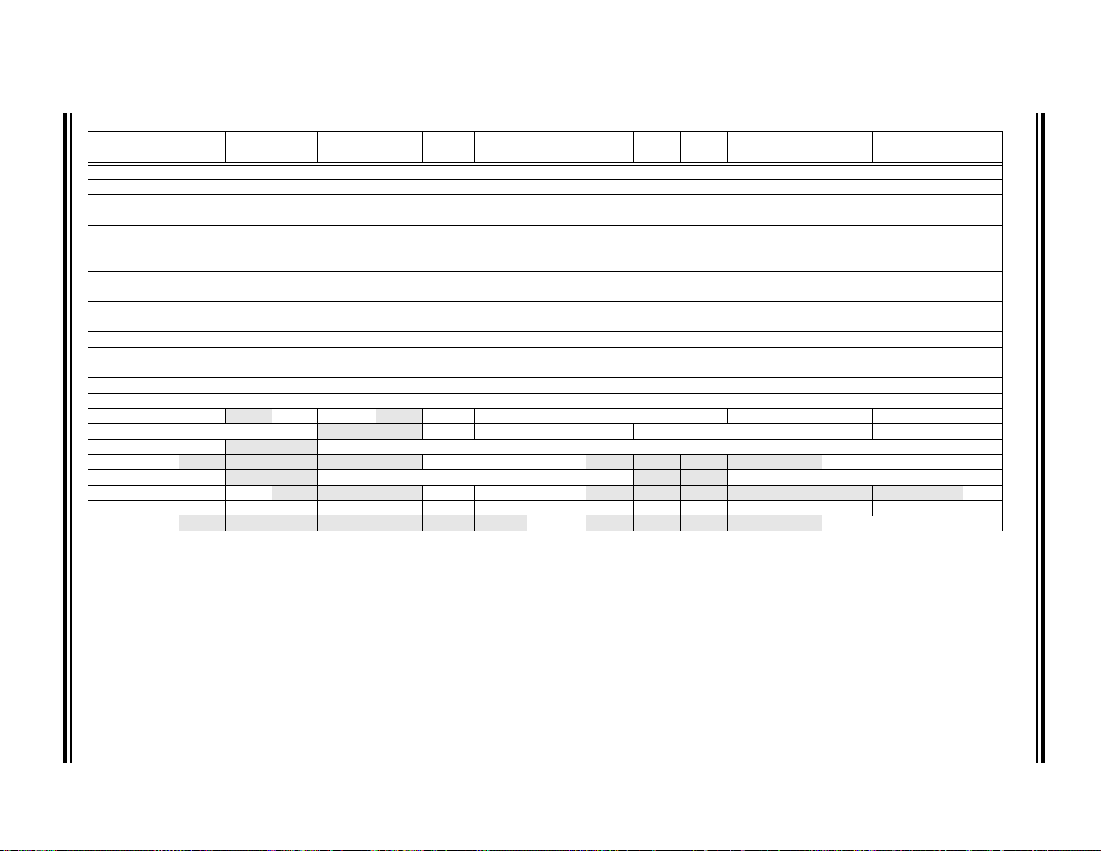
© 2011-2012 Microchip Technology Inc. Preliminary DS70657E-page 83
TABLE 4-20: ADC1 REGISTER MAP
File Name Addr. Bit 15 Bit 14 Bit 13 Bit 12 Bit 11 Bit 10 Bit 9 Bit 8 Bit 7 Bit 6 Bit 5 Bit 4 Bit 3 Bit 2 Bit 1 Bit 0
ADC1BUF0 0300 ADC1 Data Buffer 0 xxxx
ADC1BUF1 0302 ADC1 Data Buffer 1 xxxx
ADC1BUF2 0304 ADC1 Data Buffer 2 xxxx
ADC1BUF3 0306 ADC1 Data Buffer 3 xxxx
ADC1BUF4 0308 ADC1 Data Buffer 4 xxxx
ADC1BUF5 030A ADC1 Data Buffer 5 xxxx
ADC1BUF6 030C ADC1 Data Buffer 6 xxxx
ADC1BUF7 030E ADC1 Data Buffer 7 xxxx
ADC1BUF8 0310 ADC1 Data Buffer 8 xxxx
ADC1BUF9 0312 ADC1 Data Buffer 9 xxxx
ADC1BUFA 0314 ADC1 Data Buffer 10 xxxx
ADC1BUFB 0316 ADC1 Data Buffer 11 xxxx
ADC1BUFC 0318 ADC1 Data Buffer 12 xxxx
ADC1BUFD 031A ADC1 Data Buffer 13 xxxx
ADC1BUFE 031C ADC1 Data Buffer 14 xxxx
ADC1BUFF 031E ADC1 Data Buffer 15 xxxx
AD1CON1 0320 ADON
AD1CON2 0322 VCFG<2:0>
AD1CON3 0324 ADRC
AD1CHS123 0326
AD1CHS0 0328 CH0NB
AD1CSSH 032E CSS31 CSS30
AD1CSSL 0330 CSS15 CSS14 CSS13 CSS12 CSS11 CSS10 CSS9 CSS8 CSS7 CSS6 CSS5 CSS4 CSS3 CSS2 CSS1 CSS0 0000
AD1CON4 0332
Legend: x = unknown value on Reset, — = unimplemented, read as ‘0’. Reset values are shown in hexadecimal.
— — — — — CH123NB<1:0> CH123SB — — — — — CH123NA<1:0> CH123SA 0000
— — — — — — — ADDMAEN — — — — —DMABL<2:0>0000
— ADSIDL ADDMABM — AD12B FORM<1:0> SSRC<2:0> SSRCG SIMSAM ASAM SAMP DONE 0000
— — CSCNA CHPS<1:0> BUFS SMPI<4:0> BUFM ALTS 0000
— — SAMC<4:0> ADCS<7:0> 0000
— — CH0SB<4:0> CH0NA — — CH0SA<4:0> 0000
— — — CSS26 CSS25 CSS24 — — — — — — — — 0000
All
Resets
dsPIC33EPXXXGP50X, dsPIC33EPXXXMC20X/50X, AND PIC24EPXXXGP/MC20X

DS70657E-page 84 Preliminary © 2011-2012 Microchip Technology Inc.
TABLE 4-21: ECAN1 REGISTER MAP WHEN WIN (C1CTRL<0>) = 0 OR 1 FOR dsPIC33EPXXXMC/GP50X DEVICES ONLY
File Name
C1CTRL1 0400
C1CTRL2 0402
C1VEC 0404
C1FCTRL 0406 DMABS<2:0>
C1FIFO 0408
C1INTF 040A
C1INTE 040C
C1EC 040E TERRCNT<7:0> RERRCNT<7:0> 0000
C1CFG1 0410
C1CFG2 0412
C1FEN1 0414 FLTEN15 FLTEN14 FLTEN13 FLTEN12 FLTEN11 FLTEN10 FLTEN9 FLTEN8 FLTEN7 FLTEN6 FLTEN5 FLTEN4 FLTEN3 FLTEN2 FLTEN1 FLTEN0 FFFF
C1FMSKSEL1 0418 F7MSK<1:0> F6MSK<1:0> F5MSK<1:0> F4MSK<1:0> F3MSK<1:0> F2MSK<1:0> F1MSK<1:0> F0MSK<1:0> 0000
C1FMSKSEL2 041A F15MSK<1:0> F14MSK<1:0> F13MSK<1:0> F12MSK<1:0> F11MSK<1:0> F10MSK<1:0> F9MSK<1:0> F8MSK<1:0> 0000
Legend: — = unimplemented, read as ‘0’. Reset values are shown in hexadecimal.
Addr.
Bit 15 Bit 14 Bit 13 Bit 12 Bit 11 Bit 10 Bit 9 Bit 8 Bit 7 Bit 6 Bit 5 Bit 4 Bit 3 Bit 2 Bit 1 Bit 0
— — CSIDL ABAT CANCKS REQOP<2:0> OPMODE<2:0> — CANCAP — —WIN0480
— — — — — — — — — — — DNCNT<4:0> 0000
— — —FILHIT<4:0> — ICODE<6:0> 0040
— — — — — — — —FSA<4:0>0000
— —FBP<5:0> — — FNRB<5:0> 0000
— — TXBO TXBP RXBP TXWAR RXWAR EWARN IVRIF WAKIF ERRIF — FIFOIF RBOVIF RBIF TBIF 0000
— — — — — — — — IVRIE WAKIE ERRIE — FIFOIE RBOVIE RBIE TBIE 0000
— — — — — — — — SJW<1:0> BRP<5:0> 0000
—WAKFIL— — — SEG2PH<2:0> SEG2PHTS SAM SEG1PH<2:0> PRSEG<2:0> 0000
All
Resets
TABLE 4-22: ECAN1 REGISTER MAP WHEN WIN (C1CTRL<0>) = 0 FOR dsPIC33EPXXXMC/GP50X DEVICES ONLY
File Name
C1RXFUL1 0420 RXFUL15 RXFUL14 RXFUL13 RXFUL12 RXFUL11 RXFUL10 RXFUL9 RXFUL8 RXFUL7 RXFUL6 RXFUL5 RXFUL4 RXFUL3 RXFUL2 RXFUL1 RXFUL0 0000
C1RXFUL2 0422 RXFUL31 RXFUL30 RXFUL29 RXFUL28 RXFUL27 RXFUL26 RXFUL25 RXFUL24 RXFUL23 RXFUL22 RXFUL21 RXFUL20 RXFUL19 RXFUL18 RXFUL17 RXFUL16 0000
C1RXOVF1 0428 RXOVF15 RXOVF14 RXOVF13 RXOVF12 RXOVF11 RXOVF10 RXOVF9 RXOVF8 RXOVF7 RXOVF6 RXOVF5 RXOVF4 RXOVF3 RXOVF2 RXOVF1 RXOVF0 0000
C1RXOVF2 042A RXOVF31 RXOVF30 RXOVF29 RXOVF28 RXOVF27 RXOVF26 RXOVF25 RXOVF24 RXOVF23 RXOVF22 RXOVF21 RXOVF20 RXOVF19 RXOVF18 RXOVF17 RXOVF16 0000
C1TR01CON 0430 TXEN1 TXABT1 TXLARB1 TXERR1 TXREQ1 RTREN1 TX1PRI<1:0> TXEN0 TXABAT0 TXLARB0 TXERR0 TXREQ0 RTREN0 TX0PRI<1:0> 0000
C1TR23CON 0432 TXEN3 TXABT3 TXLARB3 TXERR3 TXREQ3 RTREN3 TX3PRI<1:0> TXEN2 TXABAT2 TXLARB2 TXERR2 TXREQ2 RTREN2 TX2PRI<1:0> 0000
C1TR45CON 0434 TXEN5 TXABT5 TXLARB5 TXERR5 TXREQ5 RTREN5 TX5PRI<1:0> TXEN4 TXABAT4 TXLARB4 TXERR4 TXREQ4 RTREN4 TX4PRI<1:0> 0000
C1TR67CON 0436 TXEN7 TXABT7 TXLARB7 TXERR7 TXREQ7 RTREN7 TX7PRI<1:0> TXEN6 TXABAT6 TXLARB6 TXERR6 TXREQ6 RTREN6 TX6PRI<1:0> xxxx
C1RXD 0440 Received Data Word xxxx
C1TXD 0442 Transmit Data Word xxxx
Legend: x = unknown value on Reset, — = unimplemented, read as ‘0’. Reset values are shown in hexadecimal.
Addr
Bit 15 Bit 14 Bit 13 Bit 12 Bit 11 Bit 10 Bit 9 Bit 8 Bit 7 Bit 6 Bit 5 Bit 4 Bit 3 Bit 2 Bit 1 Bit 0
0400-
041E
See definition when WIN = x
All
Resets
dsPIC33EPXXXGP50X, dsPIC33EPXXXMC20X/50X, AND PIC24EPXXXGP/MC20X

© 2011-2012 Microchip Technology Inc. Preliminary DS70657E-page 85
TABLE 4-23: ECAN1 REGISTER MAP WHEN WIN (C1CTRL<0>) = 1 FOR dsPIC33EPXXXMC/GP50X DEVICES ONLY
File Name Addr Bit 15 Bit 14 Bit 13 Bit 12 Bit 11 Bit 10 Bit 9 Bit 8 Bit 7 Bit 6 Bit 5 Bit 4 Bit 3 Bit 2 Bit 1 Bit 0
0400041E
C1BUFPNT1 0420 F3BP<3:0> F2BP<3:0> F1BP<3:0> F0BP<3:0> 0000
C1BUFPNT2 0422 F7BP<3:0> F6BP<3:0> F5BP<3:0> F4BP<3:0> 0000
C1BUFPNT3 0424 F11BP<3:0> F10BP<3:0> F9BP<3:0> F8BP<3:0> 0000
C1BUFPNT4 0426 F15BP<3:0> F14BP<3:0> F13BP<3:0> F12BP<3:0> 0000
C1RXM0SID 0430 SID<10:3> SID<2:0>
C1RXM0EID 0432 EID<15:8> EID<7:0> xxxx
C1RXM1SID 0434 SID<10:3> SID<2:0>
C1RXM1EID 0436 EID<15:8> EID<7:0> xxxx
C1RXM2SID 0438 SID<10:3> SID<2:0>
C1RXM2EID 043A EID<15:8> EID<7:0> xxxx
C1RXF0SID 0440 SID<10:3> SID<2:0>
C1RXF0EID 0442 EID<15:8> EID<7:0> xxxx
C1RXF1SID 0444 SID<10:3> SID<2:0>
C1RXF1EID 0446 EID<15:8> EID<7:0> xxxx
C1RXF2SID 0448 SID<10:3> SID<2:0>
C1RXF2EID 044A EID<15:8> EID<7:0> xxxx
C1RXF3SID 044C SID<10:3> SID<2:0>
C1RXF3EID 044E EID<15:8> EID<7:0> xxxx
C1RXF4SID 0450 SID<10:3> SID<2:0>
C1RXF4EID 0452 EID<15:8> EID<7:0> xxxx
C1RXF5SID 0454 SID<10:3> SID<2:0>
C1RXF5EID 0456 EID<15:8> EID<7:0> xxxx
C1RXF6SID 0458 SID<10:3> SID<2:0>
C1RXF6EID 045A EID<15:8> EID<7:0> xxxx
C1RXF7SID 045C SID<10:3> SID<2:0>
C1RXF7EID 045E EID<15:8> EID<7:0> xxxx
C1RXF8SID 0460 SID<10:3> SID<2:0>
C1RXF8EID 0462 EID<15:8> EID<7:0> xxxx
C1RXF9SID 0464 SID<10:3> SID<2:0>
C1RXF9EID 0466 EID<15:8> EID<7:0> xxxx
C1RXF10SID 0468 SID<10:3> SID<2:0>
C1RXF10EID 046A EID<15:8> EID<7:0> xxxx
C1RXF11SID 046C SID<10:3> SID<2:0>
C1RXF11EID 046E EID<15:8> EID<7:0> xxxx
C1RXF12SID 0470 SID<10:3> SID<2:0>
C1RXF12EID 0472 EID<15:8> EID<7:0> xxxx
Legend: x = unknown value on Reset, — = unimplemented, read as ‘0’. Reset values are shown in hexadecimal.
See definition when WIN = x
—MIDE— EID<17:16> xxxx
—MIDE— EID<17:16> xxxx
—MIDE— EID<17:16> xxxx
—EXIDE— EID<17:16> xxxx
—EXIDE— EID<17:16> xxxx
—EXIDE— EID<17:16> xxxx
—EXIDE— EID<17:16> xxxx
—EXIDE— EID<17:16> xxxx
—EXIDE— EID<17:16> xxxx
—EXIDE— EID<17:16> xxxx
—EXIDE— EID<17:16> xxxx
—EXIDE— EID<17:16> xxxx
—EXIDE— EID<17:16> xxxx
—EXIDE— EID<17:16> xxxx
—EXIDE— EID<17:16> xxxx
—EXIDE— EID<17:16> xxxx
All
Resets
dsPIC33EPXXXGP50X, dsPIC33EPXXXMC20X/50X, AND PIC24EPXXXGP/MC20X
DS70657E-page 86 Preliminary © 2011-2012 Microchip Technology Inc.
TABLE 4-23: ECAN1 REGISTER MAP WHEN WIN (C1CTRL<0>) = 1 FOR dsPIC33EPXXXMC/GP50X DEVICES ONLY (CONTINUED)
File Name Addr Bit 15 Bit 14 Bit 13 Bit 12 Bit 11 Bit 10 Bit 9 Bit 8 Bit 7 Bit 6 Bit 5 Bit 4 Bit 3 Bit 2 Bit 1 Bit 0
C1RXF13SID 0474 SID<10:3> SID<2:0> —EXIDE— EID<17:16> xxxx
C1RXF13EID 0476 EID<15:8> EID<7:0> xxxx
C1RXF14SID 0478 SID<10:3> SID<2:0>
C1RXF14EID 047A EID<15:8> EID<7:0> xxxx
C1RXF15SID 047C SID<10:3> SID<2:0>
C1RXF15EID 047E EID<15:8> EID<7:0> xxxx
Legend: x = unknown value on Reset, — = unimplemented, read as ‘0’. Reset values are shown in hexadecimal.
—EXIDE— EID<17:16> xxxx
—EXIDE— EID<17:16> xxxx
All
Resets
dsPIC33EPXXXGP50X, dsPIC33EPXXXMC20X/50X, AND PIC24EPXXXGP/MC20X

© 2011-2012 Microchip Technology Inc. Preliminary DS70657E-page 87
TABLE 4-24: CRC REGISTER MAP
File Name Addr. Bit 15 Bit 14 Bit 13 Bit 12 Bit 11 Bit 10 Bit 9 Bit 8 Bit 7 Bit 6 Bit 5 Bit 4 Bit 3 Bit 2 Bit 1 Bit 0
CRCCON1 0640
CRCCON2 0642
CRCXORL 0644
CRCXORH 0646
CRCDATL 0648
CRCDATH 064A
CRCWDATL 064C
CRCWDATH 064E
Legend: — = unimplemented, read as ‘0’. Shaded bits are not used in the operation of the programmable CRC module.
CRCEN
— — —
— CSIDL VWORD<4:0> CRCFUL CRCMPT CRCISEL CRCGO LENDIAN
DWIDTH<4:0>
— — —
— — —
X<15:1> —
X<23:16>
CRC Data Input Low Word
CRC Data Input High Word
CRC Result Low Word
CRC Result High Word
PLEN<4:0>
TABLE 4-25: PERIPHERAL PIN SELECT OUTPUT REGISTER MAP FOR dsPIC33EPXXXGP/MC202/502 AND PIC24EPXXXGP/MC202
DEVICES ONLY
File
Name
RPOR0 0680
RPOR1 0682
RPOR2 0684
RPOR3 0686
RPOR4 0688
Legend: x = unknown value on Reset, — = unimplemented, read as ‘0’. Reset values are shown in hexadecimal.
Addr. Bit 15 Bit 14 Bit 13 Bit 12 Bit 11 Bit 10 Bit 9 Bit 8 Bit 7 Bit 6 Bit 5 Bit 4 Bit 3 Bit 2 Bit 1 Bit 0
— — RP35R<5:0> — — RP20R<5:0> 0000
— — RP37R<5:0> — — RP36R<5:0> 0000
— — RP39R<5:0> — — RP38R<5:0> 0000
— — RP41R<5:0> — — RP40R<5:0> 0000
— — RP43R<5:0> — — RP42R<5:0> 0000
All
dsPIC33EPXXXGP50X, dsPIC33EPXXXMC20X/50X, AND PIC24EPXXXGP/MC20X
Resets
0000
0000
0000
0000
0000
0000
0000
0000
All
Resets
TABLE 4-26: PERIPHERAL PIN SELECT OUTPUT REGISTER MAP FOR dsPIC33EPXXXGP/MC203/503 AND PIC24EPXXXGP/MC203
DEVICES ONLY
File
Name
RPOR0 0680
RPOR1 0682
RPOR2 0684
RPOR3 0686
RPOR4 0688
RPOR5 068A
RPOR6 068C
Legend: x = unknown value on Reset, — = unimplemented, read as ‘0’. Reset values are shown in hexadecimal.
Addr. Bit 15 Bit 14 Bit 13 Bit 12 Bit 11 Bit 10 Bit 9 Bit 8 Bit 7 Bit 6 Bit 5 Bit 4 Bit 3 Bit 2 Bit 1 Bit 0
— — RP35R<5:0> — — RP20R<5:0> 0000
— — RP37R<5:0> — — RP36R<5:0> 0000
— — RP39R<5:0> — — RP38R<5:0> 0000
— — RP41R<5:0> — — RP40R<5:0> 0000
— — RP43R<5:0> — — RP42R<5:0> 0000
— — — — — — — — — — — — — — — — 0000
— — — — — — — — — — RP56R<5:0> 0000
All
Resets

DS70657E-page 88 Preliminary © 2011-2012 Microchip Technology Inc.
TABLE 4-27: PERIPHERAL PIN SELECT OUTPUT REGISTER MAP FOR dsPIC33EPXXXGP/MC204/504 AND PIC24EPXXXGP/MC204
DEVICES ONLY
File
Name
RPOR0 0680
RPOR1 0682
RPOR2 0684
RPOR3 0686
RPOR4 0688
RPOR5 068A
RPOR6 068C
Legend: x = unknown value on Reset, — = unimplemented, read as ‘0’. Reset values are shown in hexadecimal.
Addr. Bit 15 Bit 14 Bit 13 Bit 12 Bit 11 Bit 10 Bit 9 Bit 8 Bit 7 Bit 6 Bit 5 Bit 4 Bit 3 Bit 2 Bit 1 Bit 0
— — RP35R<5:0> — — RP20R<5:0> 0000
— — RP37R<5:0> — — RP36R<5:0> 0000
— — RP39R<5:0> — — RP38R<5:0> 0000
— — RP41R<5:0> — — RP40R<5:0> 0000
— — RP43R<5:0> — — RP42R<5:0> 0000
— — RP55R<5:0> — — RP54R<5:0> 0000
— — RP57R<5:0> — — RP56R<5:0> 0000
TABLE 4-28: PERIPHERAL PIN SELECT OUTPUT REGISTER MAP FOR dsPIC33EPXXXGP/MC206/506 AND PIC24EPXXXGP/MC206
DEVICES ONLY
File
Name
RPOR0 0680
RPOR1 0682
RPOR2 0684
RPOR3 0686
RPOR4 0688
RPOR5 068A
RPOR6 068C
RPOR7 068E
RPOR8 0690
RPOR9 0692
Legend: x = unknown value on Reset, — = unimplemented, read as ‘0’. Reset values are shown in hexadecimal.
Addr. Bit 15 Bit 14 Bit 13 Bit 12 Bit 11 Bit 10 Bit 9 Bit 8 Bit 7 Bit 6 Bit 5 Bit 4 Bit 3 Bit 2 Bit 1 Bit 0
— — RP35R<5:0> — — RP20R<5:0> 0000
— — RP37R<5:0> — — RP36R<5:0> 0000
— — RP39R<5:0> — — RP38R<5:0> 0000
— — RP41R<5:0> — — RP40R<5:0> 0000
— — RP43R<5:0> — — RP42R<5:0> 0000
— — RP55R<5:0> — — RP54R<5:0> 0000
— — RP57R<5:0> — — RP56R<5:0> 0000
— — RP97R<5:0> — — — — — — — — 0000
— — RP118R<5:0> — — — — — — — — 0000
— — — — — — — — — — RP120R<5:0> 0000
dsPIC33EPXXXGP50X, dsPIC33EPXXXMC20X/50X, AND PIC24EPXXXGP/MC20X
All
Resets
All
Resets
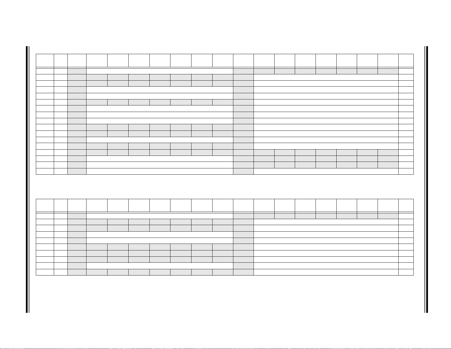
© 2011-2012 Microchip Technology Inc. Preliminary DS70657E-page 89
TABLE 4-29: PERIPHERAL PIN SELECT INPUT REGISTER MAP FOR PIC24EPXXXMC20X DEVICES ONLY
File
Addr. Bit 15 Bit 14 Bit 13 Bit 12 Bit 11 Bit 10 Bit 9 Bit 8 Bit 7 Bit 6 Bit 5 Bit 4 Bit 3 Bit 2 Bit 1 Bit 0
Name
RPINR0 06A0 —INT1R<6:0> — — — — — — — — 0000
RPINR1 06A2
RPINR3 06A6
RPINR7 06AE
RPINR8 06B0
RPINR11 06B6
RPINR12 06B8
RPINR14 06BC
RPINR15 06BE
RPINR18 06C4
RPINR19 06C6
RPINR22 06CC
RPINR23 06CE
RPINR26 06D4
RPINR37 06EA
RPINR38 06EC
RPINR39 06EE
Legend: x = unknown value on Reset, — = unimplemented, read as ‘0’. Reset values are shown in hexadecimal.
— — — — — — — — —INT2R<6:0>0000
— — — — — — — — —T2CKR<6:0>0000
—IC2R<6:0> —IC1R<6:0>0000
—IC4R<6:0> —IC3R<6:0>0000
— — — — — — — — —OCFAR<6:0>0000
—FLT2R<6:0> —FLT1R<6:0>0000
—QEB1R<6:0> —QEA1R<6:0>0000
— HOME1R<6:0> — INDX1R<6:0> 0000
— — — — — — — — —U1RXR<6:0>0000
— — — — — — — — —U2RXR<6:0>0000
— SCK2INR<6:0> —SDI2R<6:0>0000
— — — — — — — — — SS2R<6:0> 0000
— — — — — — — — — — — — — — — — 0000
— SYNCI1R<6:0> — — — — — — — — 0000
—DTCMP1R<6:0> — — — — — — — — 0000
—DTCMP3R<6:0> —DTCMP2R<6:0>0000
All
Resets
TABLE 4-30: PERIPHERAL PIN SELECT INPUT REGISTER MAP FOR PIC24EPXXXGP20X DEVICES ONLY
File
Addr. Bit 15 Bit 14 Bit 13 Bit 12 Bit 11 Bit 10 Bit 9 Bit 8 Bit 7 Bit 6 Bit 5 Bit 4 Bit 3 Bit 2 Bit 1 Bit 0
Name
RPINR0 06A0 —INT1R<6:0> — — — — — — — — 0000
RPINR1 06A2
RPINR3 06A6
RPINR7 06AE
RPINR8 06B0
RPINR11 06B6
RPINR18 06C4
RPINR19 06C6
RPINR22 06CC
RPINR23 06CE
Legend: x = unknown value on Reset, — = unimplemented, read as ‘0’. Reset values are shown in hexadecimal.
— — — — — — — — —INT2R<6:0>0000
— — — — — — — — —T2CKR<6:0>0000
—IC2R<6:0> —IC1R<6:0>0000
—IC4R<6:0> —IC3R<6:0>0000
— — — — — — — — —OCFAR<6:0>0000
— — — — — — — — —U1RXR<6:0>0000
— — — — — — — — —U2RXR<6:0>0000
— SCK2INR<6:0> —SDI2R<6:0>0000
— — — — — — — — — SS2R<6:0> 0000
All
Resets
dsPIC33EPXXXGP50X, dsPIC33EPXXXMC20X/50X, AND PIC24EPXXXGP/MC20X

DS70657E-page 90 Preliminary © 2011-2012 Microchip Technology Inc.
TABLE 4-31: PERIPHERAL PIN SELECT INPUT REGISTER MAP FOR dsPIC33EPXXXGP50X DEVICES ONLY
File
Addr. Bit 15 Bit 14 Bit 13 Bit 12 Bit 11 Bit 10 Bit 9 Bit 8 Bit 7 Bit 6 Bit 5 Bit 4 Bit 3 Bit 2 Bit 1 Bit 0
Name
RPINR0 06A0 —INT1R<6:0> — — — — — — — — 0000
RPINR1 06A2
RPINR3 06A6
RPINR7 06AE
RPINR8 06B0
RPINR11 06B6
RPINR18 06C4
RPINR19 06C6
RPINR22 06CC
RPINR23 06CE
RPINR26 06D4
Legend: x = unknown value on Reset, — = unimplemented, read as ‘0’. Reset values are shown in hexadecimal.
— — — — — — — — —INT2R<6:0>0000
— — — — — — — — —T2CKR<6:0>0000
— IC2R<6:0> — IC1R<6:0> 0000
— IC4R<6:0> — IC3R<6:0> 0000
— — — — — — — — —OCFAR<6:0>0000
— — — — — — — — —U1RXR<6:0>0000
— — — — — — — — —U2RXR<6:0>0000
— SCK2INR<6:0> —SDI2R<6:0>0000
— — — — — — — — — SS2R<6:0> 0000
— — — — — — — — —C1RXR<6:0>0000
All
Resets
TABLE 4-32: PERIPHERAL PIN SELECT INPUT REGISTER MAP FOR dsPIC33EPXXXMC50X DEVICES ONLY
File
Addr. Bit 15 Bit 14 Bit 13 Bit 12 Bit 11 Bit 10 Bit 9 Bit 8 Bit 7 Bit 6 Bit 5 Bit 4 Bit 3 Bit 2 Bit 1 Bit 0
Name
RPINR0 06A0 —INT1R<6:0> — — — — — — — — 0000
RPINR1 06A2
RPINR3 06A6
RPINR7 06AE
RPINR8 06B0
RPINR11 06B6
RPINR12 06B8
RPINR14 06BC
RPINR15 06BE
RPINR18 06C4
RPINR19 06C6
RPINR22 06CC
RPINR23 06CE
RPINR26 06D4
RPINR37 06EA
RPINR38 06EC
RPINR39 06EE
Legend: x = unknown value on Reset, — = unimplemented, read as ‘0’. Reset values are shown in hexadecimal.
— — — — — — — — —INT2R<6:0>0000
— — — — — — — — —T2CKR<6:0>0000
— IC2R<6:0> — IC1R<6:0> 0000
— IC4R<6:0> — IC3R<6:0> 0000
— — — — — — — — —OCFAR<6:0>0000
—FLT2R<6:0> —FLT1R<6:0>0000
—QEB1R<6:0> — QEA1R<6:0> 0000
— HOME1R<6:0> — INDX1R<6:0> 0000
— — — — — — — — —U1RXR<6:0>0000
— — — — — — — — —U2RXR<6:0>0000
— SCK2INR<6:0> —SDI2R<6:0>0000
— — — — — — — — — SS2R<6:0> 0000
— — — — — — — — —C1RXR<6:0>0000
— SYNCI1R<6:0> — — — — — — — — 0000
—DTCMP1R<6:0> — — — — — — — — 0000
—DTCMP3R<6:0> —DTCMP2R<6:0>0000
All
Resets
dsPIC33EPXXXGP50X, dsPIC33EPXXXMC20X/50X, AND PIC24EPXXXGP/MC20X
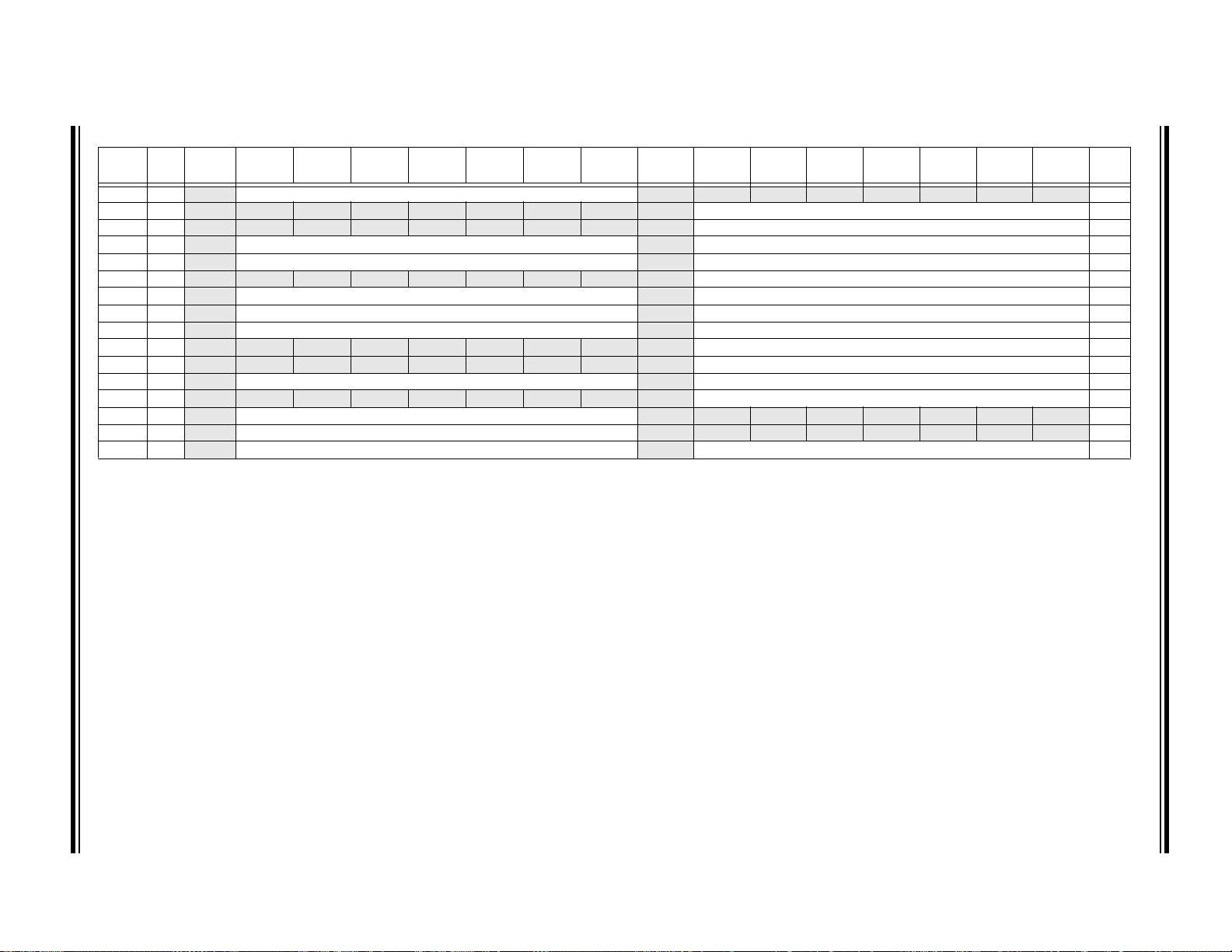
© 2011-2012 Microchip Technology Inc. Preliminary DS70657E-page 91
TABLE 4-33: PERIPHERAL PIN SELECT INPUT REGISTER MAP FOR dsPIC33EPXXXMC20X DEVICES ONLY
File
Addr. Bit 15 Bit 14 Bit 13 Bit 12 Bit 11 Bit 10 Bit 9 Bit 8 Bit 7 Bit 6 Bit 5 Bit 4 Bit 3 Bit 2 Bit 1 Bit 0
Name
RPINR0 06A0 —INT1R<6:0> — — — — — — — — 0000
RPINR1 06A2
RPINR3 06A6
RPINR7 06AE
RPINR8 06B0
RPINR11 06B6
RPINR12 06B8
RPINR14 06BC
RPINR15 06BE
RPINR18 06C4
RPINR19 06C6
RPINR22 06CC
RPINR23 06CE
RPINR37 06EA
RPINR38 06EC
RPINR39 06EE
Legend: x = unknown value on Reset, — = unimplemented, read as ‘0’. Reset values are shown in hexadecimal.
— — — — — — — — —INT2R<6:0>0000
— — — — — — — — —T2CKR<6:0>0000
— IC2R<6:0> — IC1R<6:0> 0000
— IC4R<6:0> — IC3R<6:0> 0000
— — — — — — — — —OCFAR<6:0>0000
—FLT2R<6:0> —FLT1R<6:0>0000
—QEB1R<6:0> — QEA1R<6:0> 0000
— HOME1R<6:0> — INDX1R<6:0> 0000
— — — — — — — — —U1RXR<6:0>0000
— — — — — — — — —U2RXR<6:0>0000
— SCK2INR<6:0> —SDI2R<6:0>0000
— — — — — — — — — SS2R<6:0> 0000
— SYNCI1R<6:0> — — — — — — — — 0000
—DTCMP1R<6:0> — — — — — — — — 0000
—DTCMP3R<6:0> —DTCMP2R<6:0>0000
All
Resets
dsPIC33EPXXXGP50X, dsPIC33EPXXXMC20X/50X, AND PIC24EPXXXGP/MC20X

DS70657E-page 92 Preliminary © 2011-2012 Microchip Technology Inc.
TABLE 4-34: NVM REGISTER MAP
File Name Addr. Bit 15 Bit 14 Bit 13 Bit 12 Bit 11 Bit 10 Bit 9 Bit 8 Bit 7 Bit 6 Bit 5 Bit 4 Bit 3 Bit 2 Bit 1 Bit 0
NVMCON 0728 WR WREN WRERR NVMSIDL
NVMADR 072A NVMADR<15:0>
NVMADRU 072C
NVMKEY 072E
Legend: x = unknown value on Reset, — = unimplemented, read as ‘0’. Reset values are shown in hexadecimal.
— — — — — — — — NVMADR<23:16>
— — — — — — — — NVMKEY<7:0>
— — — — — — — — NVMOP<3:0>
TABLE 4-35: SYSTEM CONTROL REGISTER MAP
File Name Addr. Bit 15 Bit 14 Bit 13 Bit 12 Bit 11 Bit 10 Bit 9 Bit 8 Bit 7 Bit 6 Bit 5 Bit 4 Bit 3 Bit 2 Bit 1 Bit 0
RCON 0740 TRAPR IOPUWR
OSCCON 0742 — COSC<2:0> — NOSC<2:0> CLKLOCK IOLOCK LOCK —CF— — OSWEN
CLKDIV 0744 ROI DOZE<2:0> DOZEN FRCDIV<2:0> PLLPOST<1:0> — PLLPRE<4:0>
PLLFBD 0746
OSCTUN 0748
Legend: x = unknown value on Reset, — = unimplemented, read as ‘0’. Reset values are shown in hexadecimal.
Note 1: RCON register reset values dependent on type of reset.
2: OSCCON register reset values dependent on configuration fuses, and by type of reset.
— — — — — — — PLLDIV<8:0>
— — — — — — — — — — TUN<5:0>
— —VREGSF — CM VREGS EXTR SWR SWDTEN WDTO SLEEP IDLE BOR POR
TABLE 4-36: REFERENCE CLOCK REGISTER MAP
File Name Addr. Bit 15 Bit 14 Bit 13 Bit 12 Bit 11 Bit 10 Bit 9 Bit 8 Bit 7 Bit 6 Bit 5 Bit 4 Bit 3 Bit 2 Bit 1 Bit 0 All
REFOCON
Legend: x = unknown value on Reset, — = unimplemented, read as ‘0’. Reset values are shown in hexadecimal.
074E ROON — ROSSLP ROSEL RODIV<3:0> — — — — — — — —
Resets
dsPIC33EPXXXGP50X, dsPIC33EPXXXMC20X/50X, AND PIC24EPXXXGP/MC20X
All
Resets
0000
0000
0000
0000
All
Resets
Note 1
Note 2
0030
0030
0000
0000

© 2011-2012 Microchip Technology Inc. Preliminary DS70657E-page 93
TABLE 4-37: PMD REGISTER MAP FOR PIC24EPXXXGP20X DEVICES ONLY
File
Addr. Bit 15 Bit 14 Bit 13 Bit 12 Bit 11 Bit 10 Bit 9 Bit 8 Bit 7 Bit 6 Bit 5 Bit 4 Bit 3 Bit 2 Bit 1 Bit 0
Name
PMD1 0760 T5MD T4MD T3MD T2MD T1MD
PMD2 0762
PMD3 0764
PMD4 0766
PMD6 076A
PMD7 076C
Legend: x = unknown value on Reset, — = unimplemented, read as ‘0’. Reset values are shown in hexadecimal.
— — — — IC4MD IC3MD IC2MD IC1MD — — — — OC4MD OC3MD OC2MD OC1MD
— — — — —CMPMD— — CRCMD — — — — —I2C2MD—
— — — — — — — — — — — —REFOMDCTMUMD— —
— — — — — — — — — — — — — — — —
— — — — — — — — — — —
— — — I2C1MD U2MD U1MD SPI2MD SPI1MD — —AD1MD
DMA0MD
DMA1MD
DMA2MD
DMA3MD
PTGMD — — —
TABLE 4-38: PMD REGISTER MAP FOR PIC24EPXXXMC20X DEVICES ONLY
File
Addr. Bit 15 Bit 14 Bit 13 Bit 12 Bit 11 Bit 10 Bit 9 Bit 8 Bit 7 Bit 6 Bit 5 Bit 4 Bit 3 Bit 2 Bit 1 Bit 0
Name
PMD1 0760 T5MD T4MD T3MD T2MD T1MD QEI1MD PWMMD
PMD2 0762
PMD3 0764
PMD4 0766
PMD6 076A
PMD7 076C
Legend: x = unknown value on Reset, — = unimplemented, read as ‘0’. Reset values are shown in hexadecimal.
— — — — IC4MD IC3MD IC2MD IC1MD — — — — OC4MD OC3MD OC2MD OC1MD
— — — — — CMPMD — — CRCMD — — — — — I2C2MD —
— — — — — — — — — — — —REFOMDCTMUMD— —
— — — — — PWM3MD PWM2MD PWM1MD — — — — — — — —
— — — — — — — — — — —
— I2C1MD U2MD U1MD SPI2MD SPI1MD — —AD1MD
DMA0MD
DMA1MD
DMA2MD
DMA3MD
PTGMD — — —
All
Resets
0000
0000
0000
0000
0000
0000
All
Resets
0000
0000
0000
0000
0000
0000
dsPIC33EPXXXGP50X, dsPIC33EPXXXMC20X/50X, AND PIC24EPXXXGP/MC20X

DS70657E-page 94 Preliminary © 2011-2012 Microchip Technology Inc.
TABLE 4-39: PMD REGISTER MAP FOR dsPIC33EPXXXGP50X DEVICES ONLY
File
Addr. Bit 15 Bit 14 Bit 13 Bit 12 Bit 11 Bit 10 Bit 9 Bit 8 Bit 7 Bit 6 Bit 5 Bit 4 Bit 3 Bit 2 Bit 1 Bit 0
Name
PMD1 0760 T5MD T4MD T3MD T2MD T1MD
PMD2 0762
PMD3 0764
PMD4 0766
PMD6 076A
PMD7 076C
Legend: x = unknown value on Reset, — = unimplemented, read as ‘0’. Reset values are shown in hexadecimal.
— — — — IC4MD IC3MD IC2MD IC1MD — — — — OC4MD OC3MD OC2MD OC1MD
— — — — —CMPMD— — CRCMD — — — — —I2C2MD—
— — — — — — — — — — — —REFOMDCTMUMD— —
— — — — — — — — — — — — — — — —
— — — — — — — — — — —
— — — I2C1MD U2MD U1MD SPI2MD SPI1MD —C1MDAD1MD
DMA0MD
DMA1MD
DMA2MD
DMA3MD
PTGMD — — —
TABLE 4-40: PMD REGISTER MAP FOR dsPIC33EPXXXMC50X DEVICES ONLY
File
Addr. Bit 15 Bit 14 Bit 13 Bit 12 Bit 11 Bit 10 Bit 9 Bit 8 Bit 7 Bit 6 Bit 5 Bit 4 Bit 3 Bit 2 Bit 1 Bit 0
Name
PMD1 0760 T5MD T4MD T3MD T2MD T1MD QEI1MD PWMMD
PMD2 0762
PMD3 0764
PMD4 0766
PMD6 076A
PMD7 076C
Legend: x = unknown value on Reset, — = unimplemented, read as ‘0’. Reset values are shown in hexadecimal.
— — — — IC4MD IC3MD IC2MD IC1MD — — — — OC4MD OC3MD OC2MD OC1MD
— — — — — CMPMD — — CRCMD — — — — — I2C2MD —
— — — — — — — — — — — —REFOMDCTMUMD— —
— — — — — PWM3MD PWM2MD PWM1MD — — — — — — — —
— — — — — — — — — — —
— I2C1MD U2MD U1MD SPI2MD SPI1MD —C1MDAD1MD
DMA0MD
DMA1MD
DMA2MD
DMA3MD
PTGMD — — —
All
Resets
0000
0000
0000
0000
0000
0000
All
Resets
0000
0000
0000
0000
0000
0000
dsPIC33EPXXXGP50X, dsPIC33EPXXXMC20X/50X, AND PIC24EPXXXGP/MC20X
TABLE 4-41: PMD REGISTER MAP FOR dsPIC33EPXXXMC20X DEVICES ONLY
File
Addr. Bit 15 Bit 14 Bit 13 Bit 12 Bit 11 Bit 10 Bit 9 Bit 8 Bit 7 Bit 6 Bit 5 Bit 4 Bit 3 Bit 2 Bit 1 Bit 0
Name
PMD1 0760 T5MD T4MD T3MD T2MD T1MD QEI1MD PWMMD
PMD2 0762
PMD3 0764
PMD4 0766
PMD6 076A
PMD7 076C
Legend: x = unknown value on Reset, — = unimplemented, read as ‘0’. Reset values are shown in hexadecimal.
— — — — IC4MD IC3MD IC2MD IC1MD — — — — OC4MD OC3MD OC2MD OC1MD
— — — — — CMPMD — — CRCMD — — — — —I2C2MD—
— — — — — — — — — — — —REFOMDCTMUMD— —
— — — — — PWM3MD PWM2MD PWM1MD — — — — — — — —
— — — — — — — — — — —
— I2C1MD U2MD U1MD SPI2MD SPI1MD — —AD1MD
DMA0MD
DMA1MD
DMA2MD
DMA3MD
PTGMD — — —
All
Resets
0000
0000
0000
0000
0000
0000

© 2011-2012 Microchip Technology Inc. Preliminary DS70657E-page 95
TABLE 4-42: OP AMP/COMPARATOR REGISTER MAP
File Name Addr. Bit 15 Bit 14 Bit 13 Bit 12 Bit 11 Bit 10 Bit 9 Bit 8 Bit 7 Bit 6 Bit 5 Bit 4 Bit 3 Bit 2 Bit 1 Bit 0
CMSTAT 0A80 PSIDL
CVRCON 0A82
CM1CON 0A84 CON COE CPOL
CM1MSKSRC 0A86
CM1MSKCON 0A88 HLMS
CM1FLTR 0A8A
CM2CON 0A8C CON COE CPOL
CM2MSKSRC 0A8E
CM2MSKCON 0A90 HLMS
CM2FLTR 0A92
CM3CON 0A94 CON COE CPOL
CM3MSKSRC 0A96
CM3MSKCON 0A98 HLMS
CM3FLTR 0A9A
CM4CON 0A9C CON COE CPOL
CM4MSKSRC 0A9E
CM4MSKCON 0AA0 HLMS
CM4FLTR 0AA2
Legend: x = unknown value on Reset, — = unimplemented, read as ‘0’. Reset values are shown in hexadecimal.
—CVR2OE — — —VREFSEL— — CVREN CVR1OE CVRR CVRSS CVR<3:0> 0000
— — — — SELSRCC<3:0> SELSRCB<3:0> SELSRCA<3:0> 0000
— — — — — — — — — CFSEL<2:0> CFLTREN CFDIV<2:0> 0000
— — — — SELSRCC<3:0> SELSRCB<3:0> SELSRCA<3:0> 0000
— — — — — — — — — CFSEL<2:0> CFLTREN CFDIV<2:0> 0000
— — — — SELSRCC<3:0> SELSRCB<3:0> SELSRCA<3:0> 0000
— — — — — — — — — CFSEL<2:0> CFLTREN CFDIV<2:0> 0000
— — — — SELSRCC<3:0> SELSRCB<3:0> SELSRCA<3:0> 0000
— — — — — — — — — CFSEL<2:0> CFLTREN CFDIV<2:0> 0000
— — — C4EVT C3EVT C2EVT C1EVT — — — — C4OUT C3OUT C2OUT C1OUT 0000
— — OPMODE CEVT COUT EVPOL<1:0> —CREF — — CCH<1:0> 0000
— OCEN OCNEN OBEN OBNEN OAEN OANEN NAGS PAGS ACEN ACNEN ABEN ABNEN AAEN AANEN 0000
— — OPMODE CEVT COUT EVPOL<1:0> —CREF — — CCH<1:0> 0000
— OCEN OCNEN OBEN OBNEN OAEN OANEN NAGS PAGS ACEN ACNEN ABEN ABNEN AAEN AANEN 0000
— — OPMODE CEVT COUT EVPOL<1:0> —CREF — — CCH<1:0> 0000
— OCEN OCNEN OBEN OBNEN OAEN OANEN NAGS PAGS ACEN ACNEN ABEN ABNEN AAEN AANEN 0000
— — — CEVT COUT EVPOL<1:0> —CREF — — CCH<1:0> 0000
— OCEN OCNEN OBEN OBNEN OAEN OANEN NAGS PAGS ACEN ACNEN ABEN ABNEN AAEN AANEN 0000
All
Resets
dsPIC33EPXXXGP50X, dsPIC33EPXXXMC20X/50X, AND PIC24EPXXXGP/MC20X
TABLE 4-43: CTMU REGISTER MAP
File Name Addr Bit 15 Bit 14 Bit 13 Bit 12 Bit 11 Bit 10 Bit 9 Bit 8 Bit 7 Bit 6 Bit 5 Bit 4 Bit 3 Bit 2 Bit 1 Bit 0
CTMUCON1 033A CTMUEN
CTMUCON2 033C EDG1MOD EDG1POL
CTMUICON 033E ITRIM<5:0> IRNG<1:0>
Legend: x = unknown value on Reset, — = unimplemented, read as ‘0’. Reset values are shown in hexadecimal.
— CTMUSIDL TGEN EDGEN EDGSEQEN IDISSEN CTTRIG — — — — — — — — 0000
— — EDG1SEL<1:0> EDG2STAT EDG1STAT EDG2MOD EDG2POL
— — — — — — — — 0000
—
—EDG2SEL<1:0>— — 0000
Resets
TABLE 4-44: JTAG INTERFACE REGISTER MAP
File Name Addr Bit 15 Bit 14 Bit 13 Bit 12 Bit 11 Bit 10 Bit 9 Bit 8 Bit 7 Bit 6 Bit 5 Bit 4 Bit 3 Bit 2 Bit 1 Bit 0 All
JDATAH 0FF0
JDATAL 0FF2 JDATAL<15:0> 0000
— — — — JDATAH<27:16> xxxx
Resets
All

DS70657E-page 96 Preliminary © 2011-2012 Microchip Technology Inc.
TABLE 4-45: DMAC REGISTER MAP
File Name Addr. Bit 15 Bit 14 Bit 13 Bit 12 Bit 11 Bit 10 Bit 9 Bit 8 Bit 7 Bit 6 Bit 5 Bit 4 Bit 3 Bit 2 Bit 1 Bit 0
DMA0CON 0B00 CHEN SIZE DIR HALF NULLW
DMA0REQ 0B02 FORCE
DMA0STAL 0B04 STA<15:0> 0000
DMA0STAH 0B06
DMA0STBL 0B08 STB<15:0> 0000
DMA0STBH 0B0A
DMA0PAD 0B0C PAD<15:0> 0000
DMA0CNT 0B0E
DMA1CON 0B10 CHEN SIZE DIR HALF NULLW
DMA1REQ 0B12 FORCE
DMA1STAL 0B14 STA<15:0> 0000
DMA1STAH 0B16
DMA1STBL 0B18 STB<15:0> 0000
DMA1STBH 0B1A
DMA1PAD 0B1C PAD<15:0> 0000
DMA1CNT 0B1E
DMA2CON 0B20 CHEN SIZE DIR HALF NULLW
DMA2REQ 0B22 FORCE
DMA2STAL 0B24 STA<15:0> 0000
DMA2STAH 0B26
DMA2STBL 0B28 STB<15:0> 0000
DMA2STBH 0B2A
DMA2PAD 0B2C PAD<15:0> 0000
DMA2CNT 0B2E
DMA3CON 0B30 CHEN SIZE DIR HALF NULLW
DMA3REQ 0B32 FORCE
DMA3STAL 0B34 STA<15:0> 0000
DMA3STAH 0B36
DMA3STBL 0B38 STB<15:0> 0000
DMA3STBH 0B3A
DMA3PAD 0B3C PAD<15:0> 0000
DMA3CNT 0B3E
DMAPWC 0BF0
DMARQC 0BF2
DMAPPS 0BF4
DMALCA 0BF6
DSADRL 0BF8 DSADR<15:0> 0000
DSADRH 0BFA
Legend: x = unknown value on Reset, — = unimplemented, read as ‘0’. Reset values are shown in hexadecimal.
— — — — — — — —STA<23:16>0000
— — — — — — — — STB<23:16> 0000
— —
— — — — — — — —STA<23:16>0000
— — — — — — — — STB<23:16> 0000
— —
— — — — — — — —STA<23:16>0000
— — — — — — — — STB<23:16> 0000
— —
— — — — — — — —STA<23:16>0000
— — — — — — — — STB<23:16> 0000
— —
— — — — — — — — — — — — PWCOL3 PWCOL2 PWCOL1 PWCOL0 0000
— — — — — — — — — — — — RQCOL3 RQCOL2 RQCOL1 RQCOL0 0000
— — — — — — — — — — — — PPST3 PPST2 PPST1 PPST0 0000
— — — — — — — — — — — —LSTCH<3:0>000F
— — — — — — — — DSADR<23:16> 0000
— — — — — — — IRQSEL<7:0> 00FF
— — — — — — — IRQSEL<7:0> 00FF
— — — — — — — IRQSEL<7:0> 00FF
— — — — — — — IRQSEL<7:0> 00FF
— — — — —AMODE<1:0>— —MODE<1:0>0000
CNT<13:0>
— — — — —AMODE<1:0>— —MODE<1:0>0000
CNT<13:0>
— — — — —AMODE<1:0>— —MODE<1:0>0000
CNT<13:0>
— — — — —AMODE<1:0>— —MODE<1:0>0000
CNT<13:0>
All
Resets
0000
0000
0000
0000
dsPIC33EPXXXGP50X, dsPIC33EPXXXMC20X/50X, AND PIC24EPXXXGP/MC20X

© 2011-2012 Microchip Technology Inc. Preliminary DS70657E-page 97
TABLE 4-46: PORTA REGISTER MAP FOR PIC24EPXXXGP/MC206 AND dsPIC33EPXXXGP/MC206/506 DEVICES ONLY
File
Addr. Bit 15 Bit 14 Bit 13 Bit 12 Bit 11 Bit 10 Bit 9 Bit 8 Bit 7 Bit 6 Bit 5 Bit 4 Bit 3 Bit 2 Bit 1 Bit 0
Name
TRISA 0E00
PORTA 0E02
LATA 0E04
ODCA 0E06
CNENA 0E08
CNPUA 0E0A
CNPDA 0E0C
ANSELA 0E0E
Legend: x = unknown value on Reset, — = unimplemented, read as ‘0’. Reset values are shown in hexadecimal.
— — — TRISA12 TRISA11 TRISA10 TRISA9 TRISA8 TRISA7 — —TRISA4 — — TRISA1 TRISA0
— — — RA12 RA11 RA10 RA9 RA8 RA7 — —RA4— —RA1RA0
— — — LATA 12 LATA 11 LATA1 0 LATA 9 LATA 8 L ATA7 — —LATA4 — — LA1TA1 LA0TA0
— — — ODCA12 ODCA11 ODCA10 ODCA9 ODCA8 ODCA7 — — ODCA4 — — ODCA1 ODCA0
— — — CNIEA12 CNIEA11 CNIEA10 CNIEA9 CNIEA8 CNIEA7 — — CNIEA4 — — CNIEA1 CNIEA0
— — — CNPUA12 CNPUA11 CNPUA10 CNPUA9 CNPUA8 CNPUA7 — — CNPUA4 — — CNPUA1 CNPUA0
— — — CNPDA12 CNPDA11 CNPDA10 CNPDA9 CNPDA8 CNPDA7 — — CNPDA4 — — CNPDA1 CNPDA0
— — — ANSA12 ANSA11 — — — — — —ANSA4— — ANSA1 ANSA0
All
Resets
1F93
0000
0000
0000
0000
0000
0000
1813
TABLE 4-47: PORTB REGISTER MAP FOR PIC24EPXXXGP/MC206 AND dsPIC33EPXXXGP/MC206/506 DEVICES ONLY
File
Addr. Bit 15 Bit 14 Bit 13 Bit 12 Bit 11 Bit 10 Bit 9 Bit 8 Bit 7 Bit 6 Bit 5 Bit 4 Bit 3 Bit 2 Bit 1 Bit 0
Name
TRISB 0E10 TRISB15 TRISB14 TRISB13 TRISB12 TRISB11 TRISB10 TRISB9 TRISB8 TRISB7 TRISB6 TRISB5 TRISB4 TRISB3 TRISB2 TRISB1 TRISB0 FFFF
PORTB 0E12 RB15 RB14 RB13 RB12 RB11 RB10 RB9 RB8 RB7 RB6 RB5 RB4 RB3 RB2 RB1 RB0 xxxx
LATB 0E14 LATB15 LATB14 LATB13 LATB12 LATB11 LATB10 LATB9 LATB8 LATB7 LATB6 LATB5 LATB4 LATB3 LATB2 LATB1 LATB0 xxxx
ODCB 0E16 ODCB15 ODCB14 ODCB13 ODCB12 ODCB11 ODCB10 ODCB9 ODCB8 ODCB7 ODCB6 ODCB5 ODCB4 ODCB3 ODCB2 ODCB1 ODCB0 0000
CNENB 0E18 CNIEB15 CNIEB14 CNIEB13 CNIEB12 CNIEB11 CNIEB10 CNIEB9 CNIEB8 CNIEB7 CNIEB6 CNIEB5 CNIEB4 CNIEB3 CNIEB2 CNIEB1 CNIEB0 0000
CNPUB 0E1A CNPUB15 CNPUB14 CNPUB13 CNPUB12 CNPUB11 CNPUB10 CNPUB9 CNPUB8 CNPUB7 CNPUB6 CNPUB5 CNPUB4 CNPUB3 CNPUB2 CNPUB1 CNPUB0 0000
CNPDB 0E1C CNPDB15 CNPDB14 CNPDB13 CNPDB12 CNPDB11 CNPDB10 CNPDB9 CNPDB8 CNPDB7 CNPDB6 CNPDB5 CNPDB4 CNPDB3 CNPDB2 CNPDB1 CNPDB0 0000
ANSELB 0E1E
Legend: x = unknown value on Reset, — = unimplemented, read as ‘0’. Reset values are shown in hexadecimal.
— — — — — — —ANSB8— — — — ANSB3 ANSB2 ANSB1 ANSB0 010F
All
Resets
dsPIC33EPXXXGP50X, dsPIC33EPXXXMC20X/50X, AND PIC24EPXXXGP/MC20X
TABLE 4-48: PORTC REGISTER MAP FOR PIC24EPXXXGP/MC206 AND dsPIC33EPXXXGP/MC206/506 DEVICES ONLY
File
Addr. Bit 15 Bit 14 Bit 13 Bit 12 Bit 11 Bit 10 Bit 9 Bit 8 Bit 7 Bit 6 Bit 5 Bit 4 Bit 3 Bit 2 Bit 1 Bit 0
Name
TRISC 0E20 TRISC15
PORTC 0E22 RC15
LATC 0E24 LATC15
ODCC 0E26 ODCC15
CNENC 0E28 CNIEC15
CNPUC 0E2A CNPUC15
CNPDC 0E2C CNPDC15
ANSELC 0E2E
Legend: x = unknown value on Reset, — = unimplemented, read as ‘0’. Reset values are shown in hexadecimal.
— — — — ANSC11 — — — — — — — — ANSC2 ANSC1 ANSC0 0807
— TRISC13 TRISC12 TRISC11 TRISC10 TRISC9 TRISC8 TRISC7 TRISC6 TRISC5 TRISC4 TRISC3 TRISC2 TRISC1 TRISC0 BFFF
— RC13 RC12 RC11 RC10 RC9 RC8 RC7 RC6 RC5 RC4 RC3 RC2 RC1 RC0 xxxx
— L ATC1 3 LATC 12 LAT C11 LATC 10 LATC 9 LAT C8 L ATC7 L ATC6 LAT C5 L ATC4 LAT C3 L ATC 2 L ATC1 L ATC0 xxxx
— ODCC13 ODCC12 ODCC11 ODCC10 ODCC9 ODCC8 ODCC7 ODCC6 ODCC5 ODCC4 ODCC3 ODCC2 ODCC1 ODCC0 0000
— CNIEC13 CNIEC12 CNIEC11 CNIEC10 CNIEC9 CNIEC8 CNIEC7 CNIEC6 CNIEC5 CNIEC4 CNIEC3 CNIEC2 CNIEC1 CNIEC0 0000
— CNPUC13 CNPUC12 CNPUC11 CNPUC10 CNPUC9 CNPUC8 CNPUC7 CNPUC6 CNPUC5 CNPUC4 CNPUC3 CNPUC2 CNPUC1 CNPUC0 0000
— CNPDC13 CNPDC12 CNPDC11 CNPDC10 CNPDC9 CNPDC8 CNPDC7 CNPDC6 CNPDC5 CNPDC4 CNPDC3 CNPDC2 CNPDC1 CNPDC0 0000
All
Resets
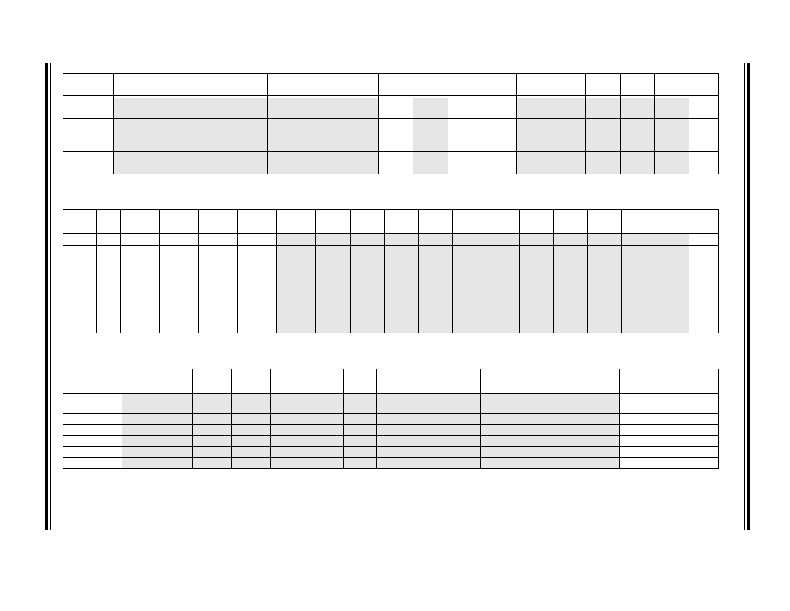
DS70657E-page 98 Preliminary © 2011-2012 Microchip Technology Inc.
TABLE 4-49: PORTD REGISTER MAP FOR PIC24EPXXXGP/MC206 AND dsPIC33EPXXXGP/MC206/506 DEVICES ONLY
File
Addr. Bit 15 Bit 14 Bit 13 Bit 12 Bit 11 Bit 10 Bit 9 Bit 8 Bit 7 Bit 6 Bit 5 Bit 4 Bit 3 Bit 2 Bit 1 Bit 0
Name
TRISD 0E30
PORTD 0E32
LATD 0E34
ODCD 0E36
CNEND 0E38
CNPUD 0E3A
CNPDD 0E3C
Legend: x = unknown value on Reset, — = unimplemented, read as ‘0’. Reset values are shown in hexadecimal.
— — — — — — —TRISD8— TRISD6 TRISD5 — — — — — 0160
— — — — — — — RD8 — RD6 RD5 — — — — — xxxx
— — — — — — —LATD8—LATD6LATD5— — — — — xxxx
— — — — — — — ODCD8 — ODCD6 ODCD5 — — — — — 0000
— — — — — — — CNIED8 — CNIED6 CNIED5 — — — — — 0000
— — — — — — — CNPUD8 — CNPUD6 CNPUD5 — — — — — 0000
— — — — — — — CNPDD8 — CNPDD6 CNPDD5 — — — — — 0000
TABLE 4-50: PORTE REGISTER MAP FOR PIC24EPXXXGP/MC206 AND dsPIC33EPXXXGP/MC206/506 DEVICES ONLY
File
Addr. Bit 15 Bit 14 Bit 13 Bit 12 Bit 11 Bit 10 Bit 9 Bit 8 Bit 7 Bit 6 Bit 5 Bit 4 Bit 3 Bit 2 Bit 1 Bit 0
Name
TRISE 0E40 TRISE15 TRISE14 TRISE13 TRISE12
PORTE 0E42 RE15 RE14 RE13 RE12
LATE 0E44 LATE15 LATE14 LATE13 LATE12
ODCE 0E46 ODCE15 ODCE14 ODCE13 ODCE12
CNENE 0E48 CNIEE15 CNIEE14 CNIEE13 CNIEE12
CNPUE 0E4A CNPUE15 CNPUE14 CNPUE13 CNPUE12
CNPDE 0E4C CNPDE15 CNPDE14 CNPDE13 CNPDE12
ANSELE 0E4E ANSE15 ANSE14 ANSE13 ANSE12
Legend: x = unknown value on Reset, — = unimplemented, read as ‘0’. Reset values are shown in hexadecimal.
— — — — — — — — — —
— — — — — — — — — — — —
— — — — — — — — — — — —
— — — — — — — — — — — —
— — — — — — — — — — — —
— — — — — — — — — — — —
— — — — — — — — — — — —
— — — — — — — — — — — —
dsPIC33EPXXXGP50X, dsPIC33EPXXXMC20X/50X, AND PIC24EPXXXGP/MC20X
All
Resets
All
Resets
—
—
F000
xxxx
xxxx
0000
0000
0000
0000
0000
TABLE 4-51: PORTF REGISTER MAP FOR PIC24EPXXXGP/MC206 AND dsPIC33EPXXXGP/MC206/506 DEVICES ONLY
File
Name
TRISF 0E50
PORTF 0E52
LATF 0E54
ODCF 0E56
CNENF 0E58
CNPUF 0E5A
CNPDF 0E5C
Legend: x = unknown value on Reset, — = unimplemented, read as ‘0’. Reset values are shown in hexadecimal.
Addr. Bit 15 Bit 14 Bit 13 Bit 12 Bit 11 Bit 10 Bit 9 Bit 8 Bit 7 Bit 6 Bit 5 Bit 4 Bit 3 Bit 2 Bit 1 Bit 0
— — — — — — — — — — — — — — TRISF1 TRISF0 0173
— — — — — — — — — — — — — —RF1RF0xxxx
— — — — — — — — — — — — — — LATF1 LATF0 xxxx
— — — — — — — — — — — — — — ODCF1 ODCF0 0000
— — — — — — — — — — — — — — CNIEF1 CNIEF0 0000
— — — — — — — — — — — — — — CNPUF1 CNPUF0 0000
— — — — — — — — — — — — — — CNPDF1 CNPDF0 0000
All
Resets

© 2011-2012 Microchip Technology Inc. Preliminary DS70657E-page 99
TABLE 4-52: PORTG REGISTER MAP FOR PIC24EPXXXGP/MC206 AND dsPIC33EPXXXGP/MC206/506 DEVICES ONLY
File
Name
TRISG 0E60
PORTG 0E62
LATG 0E64
ODCG 0E66
CNENG 0E68
CNPUG 0E6A
CNPDG 0E6C
Legend: x = unknown value on Reset, — = unimplemented, read as ‘0’. Reset values are shown in hexadecimal.
Addr. Bit 15 Bit 14 Bit 13 Bit 12 Bit 11 Bit 10 Bit 9 Bit 8 Bit 7 Bit 6 Bit 5 Bit 4 Bit 3 Bit 2 Bit 1 Bit 0
— — — — — — TRISG9 TRISG8 TRISG7 TRISG6 — — — — — — 03C0
— — — — — — RG9 RG8 RG7 RG6 — — — — — — xxxx
— — — — — — LATG9 L ATG8 L ATG7 L ATG6 — — — — — — xxxx
— — — — — — ODCG9 ODCG8 ODCG7 ODCG6 — — — — — — 0000
— — — — — — CNIEG9 CNIEG8 CNIEG7 CNIEG6 — — — — — — 0000
— — — — — — CNPUG9 CNPUG8 CNPUG7 CNPUG6 — — — — — — 0000
— — — — — — CNPDG9 CNPDG8 CNPDG7 CNPDG6 — — — — — — 0000
All
Resets
dsPIC33EPXXXGP50X, dsPIC33EPXXXMC20X/50X, AND PIC24EPXXXGP/MC20X
DS70657E-page 100 Preliminary © 2011-2012 Microchip Technology Inc.
TABLE 4-53: PORTA REGISTER MAP FOR PIC24EPXXXGP/MC204 AND dsPIC33EPXXXGP/MC204/504 DEVICES ONLY
File
Addr. Bit 15 Bit 14 Bit 13 Bit 12 Bit 11 Bit 10 Bit 9 Bit 8 Bit 7 Bit 6 Bit 5 Bit 4 Bit 3 Bit 2 Bit 1 Bit 0
Name
TRISA 0E00
PORTA 0E02
LATA 0E04
ODCA 0E06
CNENA 0E08
CNPUA 0E0A
CNPDA 0E0C
ANSELA 0E0E
Legend: x = unknown value on Reset, — = unimplemented, read as ‘0’. Reset values are shown in hexadecimal.
— — — — — TRISA10 TRISA9 TRISA8 TRISA7 — — TRISA4TRISA3TRISA2TRISA1TRISA0
— — — — — RA10RA9RA8RA7 — — RA4 RA3 RA2 RA1 RA0
— — — — — L ATA10 LATA9 L ATA8 L ATA7 — — LATA4 LATA3 LATA2 LA1TA1 LA0TA0
— — — — — ODCA10 ODCA9 ODCA8 ODCA7 — — ODCA4 ODCA3 ODCA2 ODCA1 ODCA0
— — — — — CNIEA10 CNIEA9 CNIEA8 CNIEA7 — — CNIEA4 CNIEA3 CNIEA2 CNIEA1 CNIEA0
— — — — — CNPUA10 CNPUA9 CNPUA8 CNPUA7 — — CNPUA4 CNPUA3 CNPUA2 CNPUA1 CNPUA0
— — — — — CNPDA10 CNPDA9 CNPDA8 CNPDA7 — — CNPDA4 CNPDA3 CNPDA2 CNPDA1 CNPDA0
— — — — — — — — — — —ANSA4 — — ANSA1 ANSA0
All
Resets
079F
0000
0000
0000
0000
0000
0000
0013
TABLE 4-54: PORTB REGISTER MAP FOR PIC24EPXXXGP/MC204 AND dsPIC33EPXXXGP/MC204/504 DEVICES ONLY
File
Addr. Bit 15 Bit 14 Bit 13 Bit 12 Bit 11 Bit 10 Bit 9 Bit 8 Bit 7 Bit 6 Bit 5 Bit 4 Bit 3 Bit 2 Bit 1 Bit 0
Name
TRISB 0E10 TRISB15 TRISB14 TRISB13 TRISB12 TRISB11 TRISB10 TRISB9 TRISB8 TRISB7 TRISB6 TRISB5 TRISB4 TRISB3 TRISB2 TRISB1 TRISB0 FFFF
PORTB 0E12 RB15 RB14 RB13 RB12 RB11 RB10 RB9 RB8 RB7 RB6 RB5 RB4 RB3 RB2 RB1 RB0 xxxx
LATB 0E14 LATB15 LATB14 LATB13 LATB12 LATB11 LATB10 LATB9 LATB8 LATB7 LATB6 LATB5 LATB4 LATB3 LATB2 LATB1 LATB0 xxxx
ODCB 0E16 ODCB15 ODCB14 ODCB13 ODCB12 ODCB11 ODCB10 ODCB9 ODCB8 ODCB7 ODCB6 ODCB5 ODCB4 ODCB3 ODCB2 ODCB1 ODCB0 0000
CNENB 0E18 CNIEB15 CNIEB14 CNIEB13 CNIEB12 CNIEB11 CNIEB10 CNIEB9 CNIEB8 CNIEB7 CNIEB6 CNIEB5 CNIEB4 CNIEB3 CNIEB2 CNIEB1 CNIEB0 0000
CNPUB 0E1A CNPUB15 CNPUB14 CNPUB13 CNPUB12 CNPUB11 CNPUB10 CNPUB9 CNPUB8 CNPUB7 CNPUB6 CNPUB5 CNPUB4 CNPUB3 CNPUB2 CNPUB1 CNPUB0 0000
CNPDB 0E1C CNPDB15 CNPDB14 CNPDB13 CNPDB12 CNPDB11 CNPDB10 CNPDB9 CNPDB8 CNPDB7 CNPDB6 CNPDB5 CNPDB4 CNPDB3 CNPDB2 CNPDB1 CNPDB0 0000
ANSELB 0E1E
Legend: x = unknown value on Reset, — = unimplemented, read as ‘0’. Reset values are shown in hexadecimal.
— — — — — — —ANSB8— — — — ANSB3 ANSB2 ANSB1 ANSB0 010F
All
Resets
dsPIC33EPXXXGP50X, dsPIC33EPXXXMC20X/50X, AND PIC24EPXXXGP/MC20X
TABLE 4-55: PORTC REGISTER MAP FOR PIC24EPXXXGP/MC204 AND dsPIC33EPXXXGP/MC204/504 DEVICES ONLY
File
Addr. Bit 15 Bit 14 Bit 13 Bit 12 Bit 11 Bit 10 Bit 9 Bit 8 Bit 7 Bit 6 Bit 5 Bit 4 Bit 3 Bit 2 Bit 1 Bit 0
Name
TRISC 0E20
PORTC 0E22
LATC 0E24
ODCC 0E26
CNENC 0E28
CNPUC 0E2A
CNPDC 0E2C
ANSELC 0E2E
Legend: x = unknown value on Reset, — = unimplemented, read as ‘0’. Reset values are shown in hexadecimal.
— — — — — — TRISC9 TRISC8 TRISC7 TRISC6 TRISC5 TRISC4 TRISC3 TRISC2 TRISC1 TRISC0 03FF
— — — — — — RC9 RC8 RC7 RC6 RC5 RC4 RC3 RC2 RC1 RC0 xxxx
— — — — — — L ATC9 L ATC8 LAT C7 L ATC6 LAT C5 L ATC4 LAT C3 L ATC2 L ATC1 LAT C0 xxxx
— — — — — — ODCC9 ODCC8 ODCC7 ODCC6 ODCC5 ODCC4 ODCC3 ODCC2 ODCC1 ODCC0 0000
— — — — — — CNIEC9 CNIEC8 CNIEC7 CNIEC6 CNIEC5 CNIEC4 CNIEC3 CNIEC2 CNIEC1 CNIEC0 0000
— — — — — — CNPUC9 CNPUC8 CNPUC7 CNPUC6 CNPUC5 CNPUC4 CNPUC3 CNPUC2 CNPUC1 CNPUC0 0000
— — — — — — CNPDC9 CNPDC8 CNPDC7 CNPDC6 CNPDC5 CNPDC4 CNPDC3 CNPDC2 CNPDC1 CNPDC0 0000
— — — — — — — — — — — — — ANSC2 ANSC1 ANSC0 0007
All
Resets
 Loading...