

Datasheet DSP56001RC33, DSP56001RC20, DSP56001FE33, DSP56001FE27, DSP56001FE20 Datasheet (Motorola)
...Page 1

MOTOROLA
SEMICONDUCTOR
Order this document
by DSP56001/D
TECHNICAL DATA
24-Bit General Purpose
Digital Signal Processor
The DSP56001 is a member of Motorola’s family of
HCMOS, low-power, general purpose Digital Signal
Processors. The DSP56001 features 512 words of full
speed, on-chip program RAM (PRAM) memory, two
256 word data RAMs, two preprogrammed data
ROMs, and special on -chip boot strap hardware to permit convenient loading of user programs into the program RAM. It is an off-the-sh elf part since th e program
memory is user programmable. The core of the processor consists of three execution units operating in parallel — the data ALU,
the address generation unit, and the program controller. The DSP56001 has MCU-style on-chip peripherals, program and data
memory, as well as a mem ory ex pan si on p ort. The MPU-style program mi ng m ode l an d in struction set make writ ing efficient, compact code, straightforward.
The high throughput of the DSP56001 makes it well-suited for communication, high-speed control, numeric processing, computer
and audio applications. The key features which facilitate this throughput are:
Speed
•
Precision
•
Parallelism
•
Integration
•
Invisible Pipeline
•
Instruction Set
•
DSP56000/DSP56001
•
Compatibility
Low Power
•
At 16.5 million instructions per second (MIPS) with a 33 MH z clock, the DSP 56001 can execut e
a 1024 point complex Fast Fourier Transform in1.98 milliseconds (66,240 clock cycles).
The data paths are 24 bits wide thereby providing 144 dB of dynamic range; intermediate results
held in the 56-bit accumulators can range over 336 dB.
The data ALU, address arit hme tic u nits, an d pr ogram c ontro ller ope rate in para llel s o th at an i nstruction prefetch, a 24x24-bit multip licat ion, a 56- bit add ition, two data moves , and two addres s
pointer updates using one o f three types of arithmet ic (linear, modulo, o r reverse carry) can b e
executed in a single instruction cycle. This parallelism allows a four coefficient Infinite Impulse Response (IIR) filter section to be executed in only four cycles, the theoretical minimum for a single
multiplier architecture.
In addition to the three independent executio n units, the DSP56001 has six on-ch ip memories,
three on-chip MCU style periphera ls (Se rial Co mmu nication In terfa ce, Sy nchr ono us Ser ial Inte rface, and Host Interface), a clock generator and seven buses (three address and four data), making the overall system functionally complete and powerful, but also very low cost, low power, and
compact.
The three-stage instruction pipeline is essentially invisible to the programmer thus allowing
straightforward program development in either assembly language or a high-level language such
as ANSI C.
The 62 instruction mnemonics are MC U-like making the transiti on from programming mic roprocessors to programming the DSP56001 digital signal processor as easy as possible. The orthogonal syntax supports control o f the pa ralle l exec ution unit s. This synt ax pro vide s 12,8 08, 830 d ifferent instruction variations using the 62 instruction mnemonics. The no-overhead DO instruction
and the REPEAT (REP) instruction make writing straight-line code obsolete.
The DSP56001 is identi cal to the DSP5 6000 except tha t it has 512x24-b its of on-chip progra m
RAM instead of 3.75K of program ROM; a 32x24-bit bootstrap ROM for loading the program RAM
from either a byte-wide memory mapped ROM or via the Host Interface; and the on-chip X and Y
Data ROMs have been preprogrammed as positive Mu- and A-Law to linear expansion tables and
a full, four quadrant sine wave table, respectively.
As a CMOS part, the DSP56001 is inherently very low power; however, three other features can
reduce power consumption to an exceptionally low level.
— The WAIT instruction shuts off the clock in the central processor portion of the DSP56001.
— The STOP instruction halts the internal oscillator.
— Power increases linearly (appro ximately) with frequency; thus, red ucing the clock frequency
reduces power consumption.
Pin Grid Array (PGA)
Available in an 88 pin ceramic
through-hole package.
Ceramic Quad Flat Pack (CQFP)
Available in a 132 pin, small footprint,
surface mount package.
Plastic Quad Flat Pack (PQFP)
Available in a 132 pin, small footprint,
surface mount package.
DSP56001
This document contains information on a new product. Specifications and information herein are subject to change without notice.
MOTOROLA INC., 1992
Rev. 3
May 4, 1998
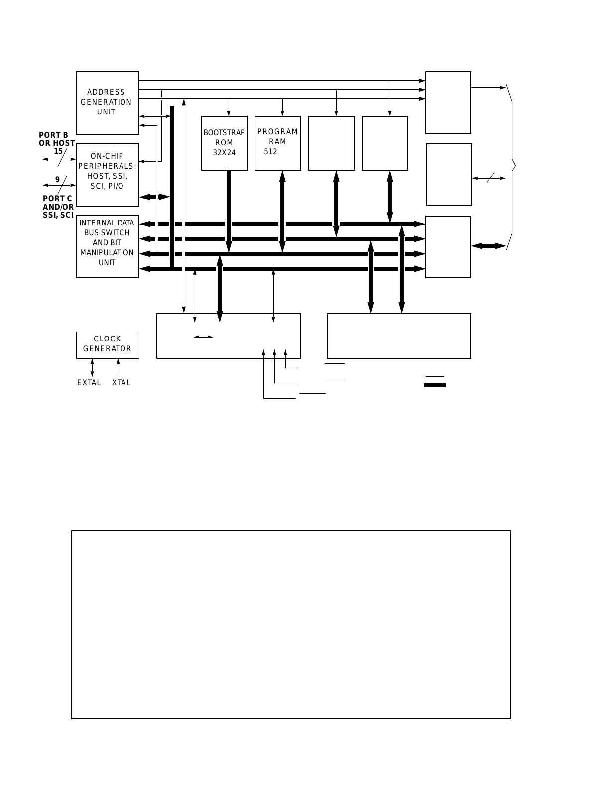
Page 2
PORT B
OR HOST
15
9
PORT C
AND/OR
SSI, SCI
ADDRESS
GENERATION
UNIT
ON-CHIP
PERIPHERALS:
HOST, SS I,
SCI, PI/O
INTERNAL DA TA
BUS SWITCH
AND BIT
MANIPUL ATION
UNIT
BOOTSTRAP
ROM
32X24
PROGRAM
RAM
512X24
YAB
XAB
PAB
X MEMORY
µ
YDB
XDB
PDB
GDB
RAM
256X24
/A ROM
256X24
Y MEMORY
RAM
256X24
SINE ROM
256X24
EXTERNAL
ADDRESS
BUS
SWITCH
BUS
CONTROL
EXTERNAL
DATA BUS
SWITCH
ADDRESS
7
DA TA
PORT A
DATA ALU
24X24+56→56-BIT MAC
16 BITS
24 BITS
CLOCK
GENERATOR
EXTAL XTA L
PROGRAM
ADDRESS
GENERATOR
PROGRAM
DECODE
CONTROLLER
PROGRAM
INTERRUPT
CONTROLLER
TWO 56-BIT ACCUMULATORS
MODB/IRQB
MODA/IRQA
RESET
Figure 1. DSP56001 Block Diagram
In the USA:
For technical assistance call:
DSP Applications Helpline (512) 891-3230
For availability and literature call your local Motorola Sales Office or Authorized Motorola Distr ibutor.
MOTOROLA
2
For free application software and information call the Dr. BuB electronic bulletin board:
9600/4800/2400/1200/300 baud
(512) 891-3771
(8 data bits, no parity, 1 stop)
In Europe, Japan and Asia Pacific
Contact your regional sales office or Motorola distributor.
DSP56001
Page 3
SIGNAL DESCRIPTION
The DSP56001 is available in 132 pin surface mount (CQFP and
PQFP) or an 88-pin pin-grid array packaging. Its input and output signals are organized into seven functional groups which are listed below
and shown in Figure 1.
Port A Address and Data Buses
Port A Bus Control
Interrupt and Mode Control
Power and Clock
Host Interface or Port B I/O
Serial Communications Interface or Port C I/O
Synchronous Serial Interface or Port C I/O
PORT A ADDRESS AND DATA BUS
Address Bus (A0-A15)
These three-state output pins specify the address for external program
and data memory accesses. To minimize power dissipation, A0-A15
do not change state when external memory spaces are not being a ccessed.
Data Bus (D0-D23)
These pins provide the bidirectional data bus for external program and
data memory accesses. D0-D23 are in the high-impedance state when
the bus grant signal is asserted.
Read Enable (RD)
This three-state output is asserted to read external memory on the
data bus D0-D23. This pin is three-stated during RESET
Write Enable (WR
)
.
This three-state output is asserted to write external memory on the
data bus D0-D23. This pin is three-stated during RESET
Bus Request (BR
The bus request input BR
/WT)
allows another device such as a processor
.
or DMA controller to become the master of external data bus D0-D23
and external address bus A0-A15. When operating mode register
(OMR) bit 7 is clear and BR
is asserted, the DSP56001 will always release the external data bus D0-D23, address bus A0-A15, and bus
control pins PS
, DS, X/Y, RD, and WR (i. e., Port A), by placing these
pins in the high-impedance state after execution of the current instruc-
pin should be pulled up when not
tion has been completed.
The BR
in use.
If OMR bit 7 is set, this pin is an input that allows an external device to
force wait states during an external Port A operation for as long as WT
is asserted.
Bus Grant (BG
/BS)
If OMR bit 7 is clear, this output is asserted to acknowledge an external
bus request after Port A has been released. If OMR bit 7 is set, this pin
is bus strobe and is asserted when the DSP accesses Port A. This pin
is three-stated during RESET
.
PORT A BUS CONTROL
Program Memory Select (PS)
This three-state output is asserted only when external program mem ory is referenced. This pin is three-stated during RESET
Data Memory Select (DS
)
.
This three-state output is asserted only when external data memory is
referenced. This pin is three-stated during RESET
Select (X/Y)
X/Y
.
This three-state output selects which external data memory space (X
or Y) is referenced by data memory select (DS
A0-A15
D0-D23
PS
DS
RD
WR
X/Y
BR/WT
BG/BS
.
HOST DATA
BUS
H0-H7
HA0
PORT A
VSS
HOST CONTROL
HA1
HA2
PORT B
DSP56001
VDD
XTAL
ed during RESET
ADDRESS
DAT A
BUS
CONTROL
). This pin is three-stat-
HR/W
HEN
HREQ
PORT C
EXTAL
IRQB
MODA/
MODB/
RESET
HACK
RXD
TXD
SCLK
SC0
SC1
SCK
SRD
STD
IRQA
Figure 2. Functional Signal Groups
INTERRUPT AND MODE CONTROL
Mode Select A/External Interrupt Request A (MODA/IRQA),
Mode Select B/External Interrupt Request B (MODB/IRQB
These two inputs have dual functions: 1) to select the initial chip operating mode and 2) to receive an interrupt request from an external
source. MODA and MODB are read and internally latched in the DSP
when the processor exits the RESET state. Therefore these two pins
should be forced into the proper state during reset. After leaving the
RESET state, the MODA and MODB pins automatically change to external interrupt requests IRQA
and IRQB. After leaving the reset state
the chip operating mode can be changed by software. IRQA
may be programmed to be level sensitive or negative edge triggered.
When edge triggered, triggering occurs at a voltage level and i s not directly related to the fall time of the interrupt signal, however, the probability of noise on IRQA
or IRQ B generating multiple interrupts increases with increasing fall time of the interrupt signal. These pins are inputs
during RESET
Reset (RESET
.
)
This Schmitt trigger input pin is used to reset the DSP56001. When
is asserted, the DSP56001 is initialized and placed in the reset
RESET
state. When the RESET
SCI
mode is latched from the MODA and MODB pins. When coming out of
signal is deasserted, the initial chip operating
reset, deassertion occurs at a voltage level and is not directly related
to the rise time of the reset signal; however, the probability of noise on
generating multiple resets increases with increasing rise time
RESET
of the reset signal.
SSI
POWER AND CLOCK
Power (Vcc), Ground (GND)
There are five sets of power and ground pins used for the four groups
of logic on the chip, two pairs for internal logic, one power and two
ground for Port A address and control pins, one power and two ground
for Port A data pins, and one pair for peripherals. Refer to the pin assignments in the
LAYOUT PRACTICES
section.
)
and IRQB
DSP56001 MOTOROLA
3
Page 4

External Clock/Crystal Input (EXTAL)
EXTAL may be used to interface the crystal oscillator input to an external crystal or an external clock.
Crystal Output (XTAL)
This output connects the internal crystal oscillator output to an external
crystal. If an external clock is used, XTAL should not be connected.
HOST INTERFACE
Host Data Bus (H0-H7)
This bidirectional data bus is used to transfer data between the host
processor and the DSP56001. This bus is an input unless enabled by
a host processor read. H0-H7 may be programmed as general purpose parallel I/O pins called PB0-PB7 when the H ost Interface is not
being used. These pins are configured as a GPIO input pins during
hardware reset.
Host Address (HA0-HA2)
These inputs provide the address selection for each Host Interface
register. HA0-HA2 may be programmed as general purpose parallel
I/O pins called PB8-PB10 when the Host Interface is not being used.
These pins are configured as a GPIO input pins during hardware reset.
Host Read/Write (HR/W
This input selects the direction of data transfer for each host processor
access. HR/W
called PB11 when the Host Interface is not being used. This pin is configured as a GPIO input pins during hardware reset.
Host Enable (HEN
This input enables a data transfer on the host data bus. When HEN
asserted and HR/W
data may be read by the host processor, When HEN
HR/W
is low, H0-H7 become inputs and host data is latched inside the
DSP when HEN
from host address decoding and an enable clock, is used to generate
. HEN may be programmed as a general purpose I/O pin called
HEN
PB12 when the Host Interface is not being used. This pin is configured
as a GPIO input pins during hardware reset.
Host Request (HREQ
This open-drain output signal is used by the DSP56001 Host Interface
to request service from the host processor, DMA controller, or simple
external controller. HREQ
I/O pin (not open-drain) called PB13 when the Host interface is not being used. HREQ
figured as a GPIO input pins during hardware reset.
Host Acknowledge (HACK
This input has two functions: 1) to receive a Host Acknowledge handshake signal for DMA transfers and, 2) to receive a Host Interrupt Acknowledge compatible with MC68000 Family processors. HACK
be programmed as a general purpose I/O pin called PB14 when the
Host Interface is not being used. This pin i s configured as a GPIO input
pins during hardware reset.
in use.
may be programmed as a general purpose I/O pin
is deasserted. Normally a chip select signal, derived
should be pulled high when not in use. This pin is con-
)
)
is high, H0-H7 become outputs, and DSP56001
)
may be programmed as a general purpose
)
should be pulled high when not
HACK
is asserted and
may
is
Transmit Data (TXD)
This output transmits serial data from the SCI Transmit Shift Register.
Data changes on the negative edge of the transmit clock. This output
is stable on the positive edge of the transmit clock. TXD may be programmed as a general purpose I/O pin called PC1 when the SCI is not
being used. This pin is configured as a GPIO input pins during hardware reset.
SCI Serial Clock (SCLK)
This bidirectional pin provides an input or output clock from which the
transmit and/or receive baud rate is derived in the asynchronous mode
and from which data is transferred in the synchronous mode. SCLK
may be programmed as a general purpose I/O pin called PC 2 when
the SCI is not being used. This pin is configured as a GPIO input pins
during hardware reset.
SYNCHRONOUS SERIAL INTERFACE (SSI)
Serial Control Zero (SC0)
This bidirectional pin is used for control by the SSI. SC0 may be programmed as a general purpose I/O pin called PC3 when the SSI is not
being used. This pin is configured as a GPIO input pins during hardware reset.
Serial Control One (SC1)
This bidirectional pin is used for control by the SSI. SC1 may be programmed as a general purpose I/O pin called PC4 when the SSI is not
being used. This pin is configured as a GPIO input pins during hardware reset.
Serial Control Two (SC2)
This bidirectional pin is used for control by the SSI. SC2 may be programmed as a general purpose I/O pin called PC5 when the SSI is not
being used. This pin is configured as a GPIO input pins during hardware reset.
SSI Serial Clock (SCK)
This bidirectional pin provides the serial bit rate clock for the SSI when
only one clock is used. SCK may be programmed as a general purpose I/O pin called PC6 when the SSI is not being used. This pin is
configured as a GPIO input pins during hardware reset.
SSI Receive Data (SRD)
This input pin receives serial data into the SSI Receive Shift Register.
SRD may be programmed as a general purpose I/O pin called PC7
when the SSI is not being used. This pin is configured as a GPIO input
pins during hardware reset.
SSI Transmit Data (STD)
This output pin transmits serial data from the SSI Transmit Shift Register. STD may be programmed as a general purpos e I/O pin called
PC8 when the SSI is not being used. This pin is configured as a GPIO
input pins during hardware reset.
SERIAL COMMUNICATIONS INTERFACE (SCI)
Receive Data (RXD)
This input receives byte-oriented data into the SCI Receive Shift Register. Input data is sampled on the positive edge of the Receive Clock.
RXD may be programmed as a general purpose I/O pin called PC0
when the SCI is not being used. This pin is configured as a GPIO input
pins during hardware reset.
MOTOROLA
4
DSP56001
Page 5
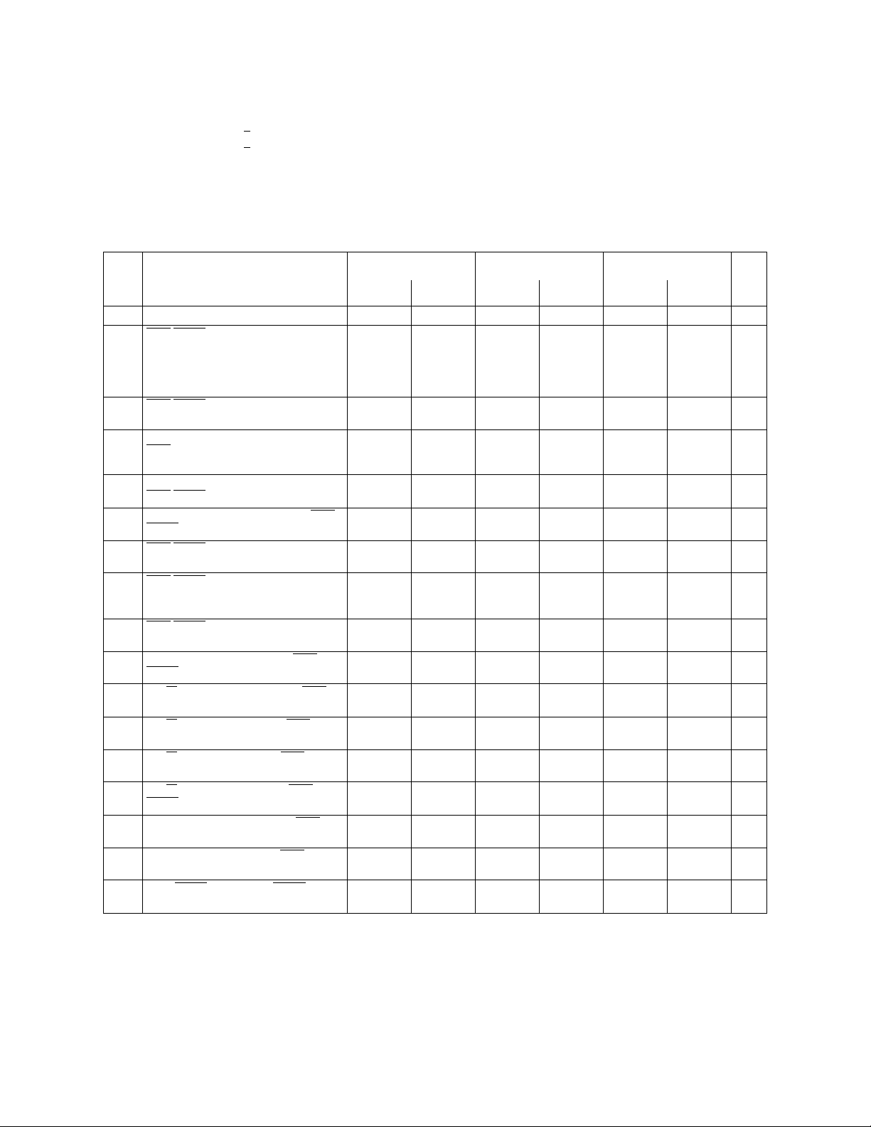
DSP56001 Electrical Characteristics
Electrical Specifications
The DSP is fabricated in high density CMOS with TTL compatible inputs and outputs.
Maximum Ratings (VSS = 0 Vdc)
Supply Voltage Vcc -0.3 to +7.0 V
All Input Voltages Vin V
Current Drain per Pin I 10 mA
excluding Vcc and V
Operating Temperature Range T
Storage Temperature Tstg -55 to +150
Rating Symbol Value Unit
SS
Maximum Electrical Ratings
Thermal Characteristics - PGA Package
Characteristics Symbol Value Rating
Thermal Resistance - Ceramic
Junction to Ambient
Junction to Case (estimated)
Thermal Characteristics - CQFP Package
Characteristics Symbol Value Rating
Thermal Resistance - Ceramic
Junction to Ambient
Junction to Case (estimated)
- 0.5 to Vcc + 0.5 V
SS
C/W
C/W
C/W
C/W
°
C
°
C
J
Θ
JA
Θ
JC
Θ
JA
Θ
JC
-40 to +105
27
6.5
40
7.0
°
°
°
°
Thermal Characteristics - PQFP Package
Characteristics Symbol Value Rating
Thermal Resistance - Plastic
Junction to Ambient
Junction to Case (estimated)
This device contains circuitry protecting against damage due to high static voltage or electrical fields; however, it is advised that normal
precautions be taken to avoid application of any voltages higher than maximum-rated voltages to this high-impedance circuit. Reliability
of operation is enhanced if unused inputs are tied to an appropriate logic voltage level (e.g., either Gnd or Vcc).
Θ
JA
Θ
JC
38
13.0
°
°
C/W
C/W
DSP56001 MOTOROLA
5
Page 6

DSP56001 Electrical Characteristics
Power Considerations
The average chip-junction temperature, TJ, in °C can be obtained from:
= TA + (P
T
J
Where:
= Ambient Temperature, °C
T
A
Θ
= Package Thermal Resistance, Junction-to-Ambient, °C/W
JA
= P
P
D
P
= I
INT
= Power Dissipation on Input and Output Pins - User Determined
P
I/O
For most applications P
between P
= K/(TJ + 273° C) (2)
P
D
× Θ
)(1)
D
JA
+ P
INT
I/O
×
Vcc, Watts - Chip Internal Power
CC
and TJ (if P
D
<< P
I/O
is neglected) is:
I/O
and can be neglected; however, P
INT
I/O
+ P
must not
INT
exceed Pd. An appropriate relationship
Solving equations (1) and (2) for K gives:
K = P
×
(T
D
+ 273° C) +
A
Θ
Where K is a constant pertaining to the particular part. K can be determined from equation (2) by meas uring P
known T
T
. Using this value of K, the values of PD and TJ can be obtained by solving equations (1) and (2) iteratively for any value of
A
. The total thermal resistance of a package (
A
heat flow from the semiconductor junction to the package (case) surface (
2
×
P
JA
D
Θ
) can be separated into two components,
JA
(3)
(at equilibrium) for a
D
Θ
and CA, representing the barrier to
Θ
) and from the case to the outside ambient (CA). These
JC
JC
terms are related by the equation:
Θ
Θ
Θ
=
+ C
JA
JC
A
is device related and cannot be influenced by the user. However, CA is user dependent and can be minimized by such thermal
JC
(4)
management techniques as heat sinks, ambient air cooling, and thermal convection. Thus, good thermal management on the part of
the user can significantly reduce C
so that
A
Θ
approximately equals
JA
Θ
. Substitution of
JC
Θ
Θ
for
JC
in equation (1) will result in a
JA
lower semiconductor junction temperature. Values for thermal resistance presented in this document, unless estimated, were derived
using the procedure described in Motorola Reliability Report 7843, “Thermal Resistance Measurement Method for MC68XX
Microcomponent Devices”, and are provided for design purposes only. Thermal measurements are complex and dependent on
procedure and setup. User-derived values for thermal resistance may differ.
Layout Practices
Each Vcc pin on the DSP56001 should be provided with a low-impedance path to + 5 volts. Each GND pin should likewise be provided
with a low-impedance path to ground. The power supply pins drive four distinct groups of logic on chip. They are:
Vcc GND Function
G12,C6 G11,B7 Internal Logic supply pins
MOTOROLA
6
L8 L6,L9 Address bus output buffer supply pins
G3 D3,J3 Data bus output buffer supply pins
C9 E11 Port B and C output buffer supply pins
Power and Ground Connections for PGA
Vcc GND Function
35, 36, 128, 129 33, 34, 130, 131 Internal Logic supply pins
63, 64 55, 56, 73, 74 Address bus output buffer supply pins
100, 101 90, 91, 111, 112 Data bus output buffer supply pins
12, 13 23, 24 Port B and C output buffer supply pins
Power and Ground Connections for CQFP and PQFP
DSP56001
Page 7

DSP56001 Electrical Characteristics
Power and Ground Connections
The Vcc power supply should be bypassed to ground using at least four 0.1 uF by- pass capacitors located either underneath the chip
or as close as possible to the four sides of the pac kage. The capacitor leads and associated printed circuit traces connecting to chip
Vcc and Gnd should be kept to less than 1/2" per capacitor lead. A four-layer board is recommended, employing two inner layers as
Vcc and Gnd planes. All output pins on the DSP56001 have fast rise and fall times — typically less than 3 ns. with a 10 pf. load. Printed
circuit (PC) trace interconnection length should be minimized in order to minimize under shoot and reflections caused by these fast
output switching times. This recommendation particularly applies to the address and data buses as well as the RD
and HEN
loads as well as parasitic capacitances due to the PC traces. Attention to proper PCB layout and bypassing becomes especially critical
in systems with higher capacitive loads because these loads create higher transient currents in the Vcc and GND circuits. Pull up/down
all unused inputs or signals that will be inputs during reset.
pins. Maximum PC trace lengths on the order of 6" are recommended. Capacitance calculations should consider all device
Signal Stability
When designing hardware to interface with the Host Interface, it is important to ensure that all signals be clean and free from noise.
Particular attention should be given to the quality of the Host Enable (HEN
asserted and should remain stable until HEN
as ground-bounce and cross-talk can inadvertently cause HEN
the full logic transition to V
storing two or more copies of a single down loaded data word. Of course, if a full logic transition occurs, the part will compl ete a normal
data transfer operation.
, the DSP56001 Host Port may not correctly update the port status information which can result in
ih min
has fully returned to the deasserted state. It is important to note that such phenomena
to temporarily rise above V
). All inputs to the port should be stable when HEN is
.
Should this occur without completing
il max
, WR, IRQA, IRQB,
DSP56001 MOTOROLA
7
Page 8
DSP56001 Electrical Characteristics
DC Electrical Characteristics (Vcc = 5.0 Vdc + 10%; TJ = -40 to +105° C at 20.5 MHz and 27 MHz)
(Vcc = 5.0 Vdc +
Characteristic Symbol Min Typ Max Unit
5%; TJ = -40 to +105° C at 33 MHz)
Supply Voltage 20, 27 MHz
33 MHz
Input High Voltage
Except EXTAL, RESET
, MODA/IRQA, MODB/IRQB
Input Low Voltage
Except EXTAL, MODA/IRQA
, MODB/IRQB
Input High Voltage EXTAL V
Input Low Voltage EXTAL V
Input High Voltage RESET
Input High Voltage MODA/IRQA
Input Low Voltage MODA/IRQA
and MODB/IRQB V
and MODB/IRQB V
Input Leakage Current
EXTAL, RESET
, MODA/IRQA, MODB/IRQB, BR
Three-State (Off-State) Input Current
Vcc 4.5
4.75
V
IH
V
IL
IHC
ILC
V
IHR
IHM
ILM
I
in
I
TSI
2.0 — Vcc V
-0.5 — 0.8 V
4.0 — Vcc V
-0.5 — 0.6 V
2.5 — Vcc V
3.5 — Vcc V
-0.5 — 2.0 V
-1 — 1 uA
-10 — 10 uA
5.0 5.5
5.25
(@2.4 V/0.4 V)
Output High Voltage (I
Output Low Voltage (I
, WR IOL = 1.6 mA; Open Drain
RD
HREQ
IOL = 6.7 mA, TXD IOL = 6.7 mA)
= -0.4 mA) V
OH
= 1.6 mA;
OL
Total Supply Current 5.25 V, 33 MHz
5 . 5 V, 27 MHz
5 . 5 V, 20 MHz
in WAIT Mode (see Note 1)
in STOP Mode (see Note 1)
OH
V
OL
I
DD33
I
DD27
I
DD20
I
DDW
I
DDS
2.4 — —V
— — 0.4 V
—
—
—
—
—
160
130
100
10
100
185
155
115
25
2000
Input Capacitance (see Note 2) Cin — 10 — pf
V
mA
mA
mA
mA
µ
A
Notes:
1. In order to obtain these results all inputs must be terminated (i.e., not allowed to float).
2. Periodically sampled and not 100% tested.
MOTOROLA
8
DSP56001
Page 9

DSP56001 Electrical Characteristics
AC Electrical Characteristics
The timing waveforms in the
all pins, except EXTAL, RESET
Characteristics
50% point of the respective input signal’s transition. DSP56001 output levels are measured with the production test machine V
V
reference levels set at 0.8 V and 2.0 V respectively.
OH
. AC timing specifications which are referenced to a device input signal are measured in production with respect to the
AC Electrical Characteristics
, MODA, and MODB. These four pins are tested using the input levels set forth in the
are tested with a VIL maximum of 0.5 V and a VIH minimum of 2.4 V for
DC Electrical
and
OL
AC Electrical Characteristics - Clock Operation
The DSP56001 system clock may be derived from the on-chip crystal oscillator as shown in Clock Figure 1, or it may be externally
supplied. An externally supplied square wave voltage source should be connected to EXTAL, leaving XTAL physically unconnected
(see Clock Figure 2) to the board or socket. The rise and fall time of this external clock should be 5 ns maximum.
Num
Frequency of Operation (EXTAL Pin)
1
External Clock Input High (tch) —
EXTAL Pin (see Note 1 and 2)
2
External Clock Input Low (tcl) —
EXTAL Pin (see Note 1 and 2)
3
Clock Cycle Time = cyc = 2T
4
Instruction Cycle Time = Icyc = 4T
Characteristics 20.5 MHz 27 MHz 33 MHz
Min Max Min Max Min Max
4.0 20.5 4.0 27.0 4.0 33.0 MHz
22 150 17 150 13.5 150 ns
22 150 17 150 13.5 150 ns
48.75 250 37 250 30.33 250 ns
97.5 500 74 500 60 500 ns
Unit
Notes:
1. External Clock Input High and External Clock Input Low are measured at 50% of the
input transition. tch and tcl are dependent on the duty cycle.
2. T = Icyc / 4 is used in the electrical characteristics. T represents an average which is
independent of the duty cycle.
DSP56001 MOTOROLA
9
Page 10
DSP56001 Electrical Characteristics
XTAL
•
•
C
EXTAL
R
•
•
C
XTAL1
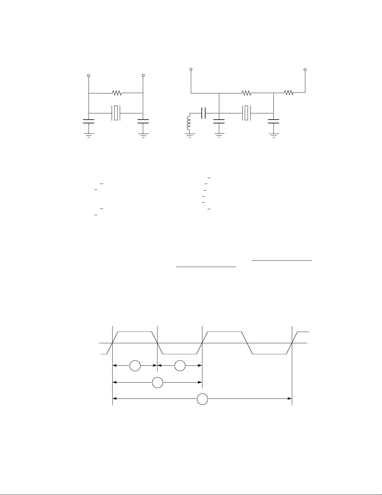
Fundamental Frequency
Crystal Oscillator
Suggested Component Values
= 4 MHz:
For f
osc
R = 680 KΩ +
C = 20 pf +
For f
osc
R = 680 KΩ +
C = 20 pf +
Notes:
(1) The suggested crystal source is ICM,
# 433163 - 4.00 (4MHz fundamental, 20
pf load) or # 436163 - 30.00 (30 MHz fundamental, 20 pf load).
10%
20%
= 30 MHz:
10%
20%
L1
EXTAL
C1
•
•
C2
rd
Overtone
3
R1
XTAL1*
XTAL
R2
•
•
C3
Crystal Oscillator
Suggested Component Values
R1 = 470 KΩ +
R2 = 330 Ω +
C1 = 0.1 µf +
C2 = 26 pf +
C3 = 20 pf +
L1 = 2.37 µH +
XTAL =33 MHz, AT cut, 20 pf load,
50Ω max series resistance
Notes:
rd
overtone crystal.
(1) *3
(2) The suggested crystal source is ICM, # 471163 - 33.00 (33
MHz 3
(3) R2 limits crystal current
(4) Reference Benjamin Parzen, The Design of Crystal and
Other Harmonic Oscillators, John Wiley& Sons, 1983
10%
10%
20%
20%
10%
10%
rd
overtone, 20 pf load).
EXTAL
Note:
MOTOROLA
10
Clock Figure 1. Crystal Oscillator Circuits
V
ILC
The midpoint is V
Clock Figure 2. External Clock Timing
1 2
3
+ 0.5 (V
ILC
IHC
- V
ILC
V
IHC
Midpoint
4
).
DSP56001
Page 11
DSP56001 Electrical Characteristics
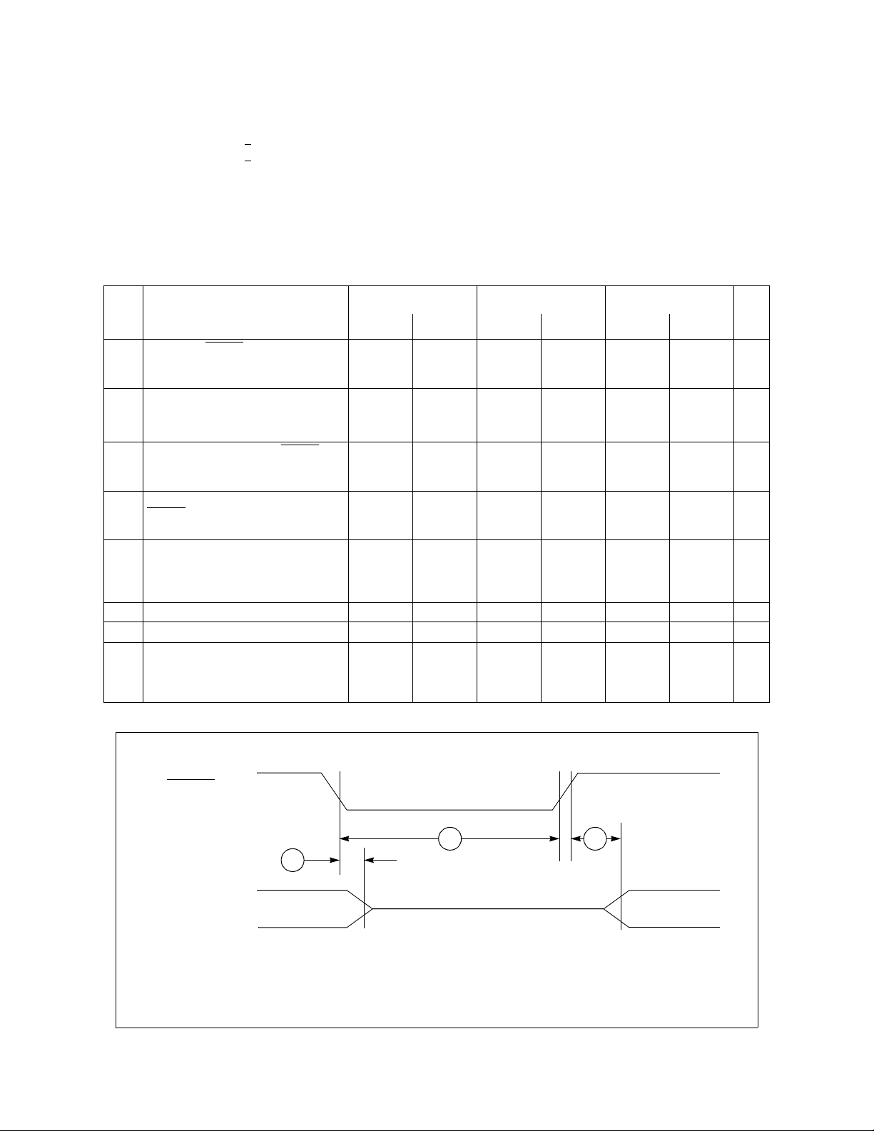
AC Electrical Characteristics - Reset, Stop, Mode Select and Interrupt Timing
(
Vcc = 5.0 Vdc +
(
Vcc = 5.0 Vdc +
(See Control Figure 1 through 8)
cyc = Clock cycle = 1/2 instruction cycle = 2 T cycles
WS = Number of wait states (1 WS = 1 cyc = 2T) programmed into external bus access
using BCR (WS = 0 - 15)
tch = Clock high period
tcl = Clock low period
10%, TJ = -40 to +105° C, CL = 50 pf + 1 TTL Load at 20.5 MHz and 27 MHz)
5%, TJ = -40 to +105° C, CL = 50 pf + 1 TTL Load at 33 MHz)
Num
Characteristics 20.5 MHz 27 MHz 33 MHz
Min Max Min Max Min Max
9 Delay from RESET Assertion to
Address High Impedance (periodically
sampled and not 100% tested)
10 Minimum Stabilization Duration
Internal Osc. (see Note 1)
11 Delay from Asynchronous RESET
Deassertion to First External Address
Output (Internal Reset Negation)
12 Synchronous Reset Setup Time from
RESET
External Clock
13 Synchronous Reset Delay Time from
the Synchronous Falling Edge of External Clock to the First External Address
Output
14 Mode Select Setup Time 100 — 77 — 62 — ns
15 Mode Select Hold Time 0 — 0 0 ns
16
Edge-Triggered Interrupt Request
16a
External Clock (see Note 2)
Deassertion to Falling Edge of
assertion
deassertion
—
75000*cyc
25*cyc
8*cyc
20
8*cyc+5
25
15
50 — 38 — 31 ns
—
—
9*cyc+40 8*cyc 9*cyc+31 8*cyc 9*cyc+25 ns
cyc-10 15 cyc-8 13 cyc-7 ns
8*cyc+30 8*cyc+5 8*cyc+23 8*cyc+5 8*cyc+19 ns
—
—
75000*cyc
25*cyc
17
10
—
—
—
—
75000*cyc
25*cyc
16
10
—
—
—
—
Unit
ns
ns
ns
ns
V
IHR
RESET
10
11
9
A0-A15
First Fetch
Control Figure 1. Reset Timing
DSP56001 MOTOROLA
11
Page 12

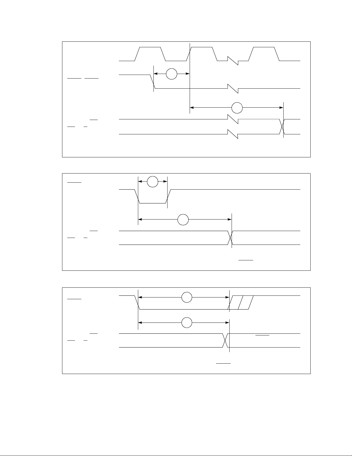
DSP56001 Electrical Characteristics
AC Electrical Characteristics - Reset, Stop, Mode Select, and Interrupt Timing
(Continued)
NOTE
IRQA
When using fast interrupts and
to prevent multiple interrupt service. To avoid these timing restrictions, the negative edge-triggered mode is recommended when using fast interrupt. Long interrupts are recommended when using level-sensitive mode.
and IRQB
are defined as
level
-sensitive, then timings 19 through 22 apply
Num
17 Delay from IRQA, IRQB Assertion to
External Memory Access Address Out
Valid Caused by First Interrupt
Instruction Fetch
Instruction Execution
18 Delay from IRQA
General Purpose Transfer Output Valid
Caused by First Interrupt Instruction
Execution
19 Delay from Address Output Valid
Caused by First Interrupt Instruction
Execution to Interrupt Request
Deassertion for Level Sensitive Fast
Interrupts
20 Delay from RD
Request Deassertion for Level
Sensitive Fast Interrupts
21 Delay from WR
Interrupt Request Deassertion for
WS>0 Level Sensitive Fast Interrupts
22 Delay from General-Purpose Output
Valid to Interrupt Request Deassertion
for Level Sensitive Fast Interrupts
- If Second Interrupt Instruction is:
Single Cycle
Two Cycle —
Characteristics 20.5 MHz 27 MHz 33 MHz
, IRQB Assertion to
Assertion to Interrupt
Assertion to WS=0
Min Max Min Max Min Max
5*cyc+tch
9*cyc+tch
11+cyc
+tch
—
—
—
—
—
—
—
—11
2*cyc+tcl+
(cyc*WS)
-44
2*cyc+
(cyc*WS)
-40
2*cyc-40
cyc+tcl+
(cyc*WS)
-40
tcl-60
(2*cyc)+tcl
-60
5*cyc+tch
9*cyc+tch
—
—
cyc
*
+tch
—2*cyc+tcl+
—
—
—
—
—
—11
(cyc*WS)
-34
2*cyc+
(cyc*WS)
-31
2*cyc-31
cyc+tcl+
(cyc*WS)
-31
tcl-46
(2*cyc)+tcl
-46
5*cyc+tch
9*cyc+tch
cyc
*
+tch
—2
—
—
—
—
—
(2*cyc)+tcl
Unit
—
—
—ns
cyc+tcl+
*
(cyc*WS)
-27
2*cyc+
(cyc*WS)
-25
2*cyc-25
cyc+tcl+
(cyc*WS)
-25
tcl-37
-37
ns
ns
ns
ns
ns
ns
ns
ns
MOTOROLA
12
DSP56001
Page 13

DSP56001 Electrical Characteristics
AC Electrical Characteristics - Reset, Stop, Mode Select, and Interrupt Timing
(Continued)
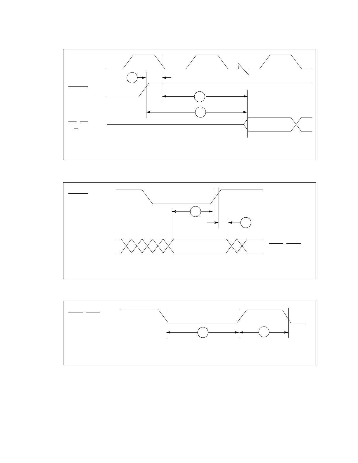
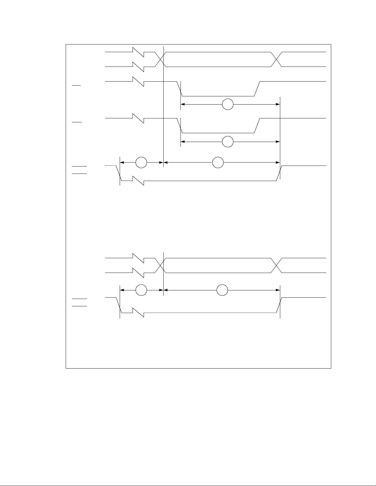
Num
Characteristics 20.5 MHz 27 MHz 33 MHz
Min Max Min Max Min Max
23 Synchronous Interrupt Setup Time
from IRQA
Synchronous Rising Edge of External
Clock (see Notes 5, 6)
24 Synchronous Interrupt Delay Time
from the Synchronous Rising Edge of
External Clock to the First External
Address Output Valid Caused by the
First Instruction Fetch after Coming out
of Wait State (see Notes 3, 5)
25 Duration for IRQA
Recover from Stop State (see Note 4) 25 — 19 — 16 — ns
26 Delay from IRQA
First Instruction (for Stop) for
Internal Osc / OMR bit 6 = 0
External Clock / OMR bit 6 = 1
(see Notes 1, 2, and 7)
27 Duration for Level Sensitive IRQA
Assertion to Fetch of First Interrupt
Instruction (for Stop) for
Internal Osc / OMR bit 6 = 0
External Clock / OMR bit 6 = 1
(see Notes 1, 2, and 7)
28 Delay from Level Sensitive IRQA
Assertion to Fetch of First Interrupt
Instruction (for Stop) for
Internal Osc / OMR bit 6 = 0
External Clock / OMR bit 6 = 1
(see Notes 1, 2, and 7)
, IRQB Assertion to the
Assertion to
Assertion to Fetch of
25 cyc-10 19 cyc-8 16 cyc-7 ns
13*cyc+
tch+8
65545*cyc
17*cyc
65533*cyc
+tcl
5*cyc+tcl
65545*cyc
17*cyc
13*cyc+
tch+30
—
—
—
—
—
—
13*cyc+
tch+6
65545*cyc
17*cyc
65533*cyc
+tcl
5*cyc+tcl
65545*cyc
17*cyc
13*cyc+
tch+23
—
—
—
—
—
—
13*cyc+
tch+5
65545*cyc
17*cyc
65533*cyc
+tcl
5*cyc+tcl
65545*cyc
17*cyc
13*cyc+
tch+19
—
—
—
—
—
—
Unit
ns
ns
ns
ns
ns
ns
ns
Notes:
1. A clock stabilization delay is required when using the on-chip crystal oscillator in
two cases:
1) after power-on reset, and
2) when recovering from Stop mode.
During this stabilization period, T will not be constant. Since this stabilization period
varies, a delay of 150,000T is typically allowed to assure that the oscillator is stabilized
before executing programs. While it is possible to set OMR bit 6 = 1 when using
the internal crystal oscillator, it is not recommended and these specifications do not
guarantee timings for that ca se. See Sec tion 8.5 i n the
DSP56000/DSP56001 Us er’s Manual
for
additional information.
2. Circuit stabilization delay is required during reset when using an external clock in
two cases:
1) after power-on reset, and
2) when recovering from Stop mode.
3. For Revision B s ilicon, the min and m ax n umbers are 12cyc+Tc h+8 a nd 12cyc+Tch+30, re spe ctively.
4. The minimum is spec ified for the du ration of an edg e triggered IRQ A
from the STOP state without having the IRQA
interrupt accepted.
interrupt required to recover
5. Timing #23 is for all IRQx interrupts while timing #24 is only when exiting WAIT.
6. Timing #23 triggers off T1 in the normal state and off T1/T3 when exiting the WAIT state.
7. The timings in the table are for Rev. C parts. The timings for Rev. C parts are shorter by 1 cyc than
the Rev. B parts when OMR6=0
.
DSP56001 MOTOROLA
13
Page 14
EXTAL
RESET
DSP56001 Electrical Characteristics
12
13
A0-A15,
DS
, PS
X/Y
RESET
MODA, MODB
11
Control Figure 2. Synchronous Reset Timing
14
15
V
IHM
V
ILM
Control Figure 3. Operating Mode Select Timing
V
IH
V
IL
V
IHR
IRQA, IRQB
IRQA, IRQB
MOTOROLA
14
16
16a
Control Figure 4. External Interrupt Timing (Negative Edge-Triggered)
DSP56001
Page 15
RD
WR
IRQA
IRQB
DSP56001 Electrical Characteristics
First Interrupt Instruction ExecutionA0-A15
20
21
1917
a) First Interrupt Instruction Execution
General
Purpose
I/O
IRQA
IRQB
18 22
b) General Purpose I/O
Control Figure 5. External Level-Sensitive Fast Interrupt Timing
DSP56001 MOTOROLA
15
Page 16
DSP56001 Electrical Characteristics
EXTAL
, IRQB
IRQA
A0-A15, DS
PS, X/Y
Control Figure 6. Synchronous Interrupt and Synchronous Wait State Timing
IRQA
25
T0, T2 T1, T3
23
24
26
A0-A15, DS,
PS
, X/Y
Control Figure 7. Recovery from Stop State Using IRQA
IRQA
A0-A15, DS,
PS
, X/Y
Control Figure 8. Recovery from Stop State Using IRQA Interrupt Service
27
28
First Instruction Fetch
First IRQA Interrupt
Instruction Fetch
MOTOROLA
16
DSP56001
Page 17

DSP56001 Electrical Characteristics
HOST PORT USAGE CONSIDERATIONS
Careful synchronization is required when reading multibit registers that are written by another asynchronous system. This is a common
problem when two asynchronous systems are connected. The situation exists in the Host port. The considerations for proper operation
are discussed below.
Host Programmer Considerations
1. Unsynchronized Reading of Receive Byte Registers
When reading receive byte registers, RXH, RXM, or RXL, the Host programmer should use interrupts or poll the RXDF flag which
indicates that data is available. This assures that the data in the receive byte registers will be stable.
2. Overwriting Transmit Byte Registers
The Host programmer should not write to the transmit byte registers, TXH, TXM, or TXL, unless the TXDE bit is set indicating that
the transmit byte registers are empty. This guarantees that the transmit byte registers will transfer valid data to the HRX register.
3. Synchronization of Status Bits from DSP to Host
HC, HREQ, DMA, HF3, HF2, TRDY, TXDE, and RXDF (refer to
DMA Interface Programming Model for descriptions of these status bits) status bits are set or cleared from inside the DSP and
read by the Host processor. The Host can read these status bits very quickly without regard to the clock rate used by the DSP,
but the possibility exists that the state of the bit could be changing during the read operation. This is generally not a system
problem, since the bit will be read correctly in the next pass of any Host polling routine.
DSP56000/DSP56001 User’s Manual
, I/O Interface section, Host/
However, if the Host asserts the HEN
(T32a), then the status is guaranteed to be stable.
A potential problem exists when reading status bits HF3 and HF2 as an encoded pair. If the DSP changes HF3 and HF2 from 00
to 11, there is a small probability that the Host could read the bits during the transition and receive 01 or 10 instead of 11. If the
combination of HF3 and HF2 has significance, the Host could read the wrong combination.
Solution:
a. Read the bits twice and check for consensus.
b. Assert HEN
4. Overwriting the Host Vector
The Host programmer should change the Host Vector register only when the Host Command bit (HC) is clear. This change will
guarantee that the DSP interrupt control logic will receive a stable vector.
5. Cancelling a Pending Host Command Exception
The Host processor may elect to clear the HC bit to cancel the Host Command Excep tion request at any time before it is
recognized by the DSP. Because the Host does not know exactly when the exception will be recognized (due to exception
processing synchronization and pipeline delays), the DSP may execute the Host exception after the HC bit is cleared. For these
reasons, the HV bits must not be changed at the same time the HC bit is cleared.
access for T31a so that status bit transitions are stabilized.
for more than timing number 31a (T31a), with a minimum cycle time of timing number 32a
DSP Programmer Considerations
1. Reading HF0 and HF1 as an Encoded Pair
DMA, HF1, HF0, and HCP, HTDE, and HRDF (refer to
Interface Programming Model for descriptions of these status bits) status bits are set or cleared by t he Host processor side of the
interface. These bits are individually synchronized to the DSP clock.
DSP56000/DSP56001 User’s Manual
, I/O Interface section, Host/DMA
A potential problem exists when reading status bits HF1 and HF2 as an encoded pair, i.e., the four combinati ons 00, 01, 10, and
11 each have significance. A very small probability exists that the DSP will read the status bits synchronized during transition.
The solution to this potential problem is to read the bits twice for consensus.
DSP56001 MOTOROLA
17
Page 18
DSP56001 Electrical Characteristics
AC Electrical Characteristics - Host I/O Ti ming
(Vcc = 5.0 Vdc + 10%, TJ = -40 to +105° C, CL = 50 pf + 1 TTL Load at 20.5 MHz and 27 MHz)
(Vcc = 5.0 Vdc +
(see Host Figures 1 through 6)
cyc = Clock cycle = 1/2 instruction cycle = 2 T cycles
tHSDL = Host Synchronization Delay Time
Active low lines should be “pulled up” in a manner consistent with the AC and DC specifications
5%, TJ = -40 to +105° C, CL = 50 pf + 1 TTL Load at 33 MHz)
Num
Characteristics 20.5 MHz 27 MHz 33 MHz
Min Max Min Max Min Max
30 Host Synchronous Delay (see Note 1) tcl cyc+tcl tcl cyc+tcl tcl cyc+tcl ns
31 HEN
32 HEN
32a Minimum Cycle Time Between Two
33 Host Data Input Setup Time Before
34 Host Data Input Hold Time After HEN
35 HEN
36 HEN
37 HEN
38 Output Data Hold Time After HEN
39 HR/W
40 HR/W
41 HR/W
42 HR/W
43 HA0-HA2 Setup Time Before HEN
44 HA0-HA2 Hold Time After HEN
45 DMA HACK
/HACK Assertion Width
(see Note 2)
a.CVR, ICR, ISR Read (see Note 4)
b.Read
c.Write
/HACK Deassertion Width
(see Note 2 and 5)
Assertion for Consecutive CVR,
HEN
ICR, and ISR Reads (see Note 2)
/HACK Deassertion
HEN
Deassertion
HACK
/HACK Assertion to Output Data
Active from High Impedance
/HACK Assertion to Output Data
Valid (periodically sampled, and not
100% tested)
/HACK Deassertion to Output
Data High Impedance
Deassertion
HACK
Low Setup Time Before HEN
Assertion
Low Hold Time After HEN
Deassertion
High Setup Time to HEN
Assertion
High Hold Time After HEN/
Deassertion
HACK
Assertion
Deassertion
Deassertion (see Note 3)
Assertion to HREQ
/
cyc+60
50
25
25 — 19 — 16 — ns
2*cyc+60 — 2*cyc+46 — 2*cyc+37 — ns
5—4—4—ns
5—4—4—ns
/
0—0—0—ns
—50—39—31ns
—35—27—22ns
5—4—4—ns
0—0—0—ns
5—4—4—ns
0—0—0—ns
5—4—4—ns
0—0—0—ns
5—4—4—ns
560446449ns
—
—
—
cyc+46
39
19
—
—
—
cyc+37
31
16
—
—
—
Unit
ns
ns
ns
MOTOROLA
18
DSP56001
Page 19
DSP56001 Electrical Characteristics
AC Electrical Characteristics - Host I/O Timing (Continued)
(Vcc = 5.0 Vdc + 10%, TJ = -40 to +105° C, CL = 50 pf + 1 TTL Load at 20.5 MHz and 27 MHz
(Vcc = 5.0 Vdc +
see Host Figures 1 through 6)
cyc = Clock cycle = 1/2 instruction cycle = 2 T cycles
tHSDL = Host Synchronization Delay Time
Active low lines should be “pulled up” in a manner consistent with the AC and DC specifications
5%, TJ = -40 to +105° C, CL = 50 pf + 1 TTL Load at 33 MHz,
Num
46 DMA HACK Deassertion to HREQ
Assertion (see Note 3)
for DMA RXL Read
for DMA TXL Write
for All Other Cases
47 Delay from HEN
Assertion for RXL Read (see Note 3)
48 Delay from HEN
Assertion for TXL Write (see Note 3)
49 Delay from HEN
Deassertion for RXL Read, TXL Write
(see Note 3)
Characteristics 20.5 MHz 27 MHz 33 MHz
Deassertion to HREQ
Deassertion to HREQ
Assertion to HREQ
Notes:
1. “Host synchronization delay (tHSDL)” is the time period required for the
DSP56001 to sample any external asynchronous input signal, determine
whether it is high or low, and synchronize it to the DSP56001 internal clock.
HOST PORT USAGE CONSIDERATIONS
2. See
3. HREQ
4. This timing must be adhered to only if two consecutive reads from one of these registers are executed.
5. It is recommended that timing #32 be 2cyc+tch+10 minimum for 20.5 MHz, 2cyc+tch+7 minimum for 27 MHz,
is pulled up by a 1kΩ resistor.
and 2cyc+tch+6 minimum for 33 MHz if two consecutive writes to TXL are executed without polling TXDE or
HREQ
.
Unit
Min Max Min Max Min Max
tHSDL+cyc
+tch+5
tHSDL+cyc+5
5
tHSDL+cyc
+tch+5
tHSDL+cyc+5 — tHSDL+cyc+4 — tHSDL+cyc+4 — ns
575470465ns
—
—
—
— tHSDL+cyc
.
tHSDL+cyc
+tch+4
tHSDL+cyc+4
4
+tch+4
—
—
—
— tHSDL+cyc
tHSDL+cyc
+tch+4
tHSDL+cyc+4
4
+tch+4
—
—
—
—ns
ns
ns
ns
EXTERNAL
3030
INTERNAL
Host Figure 1. Host Synchronization Delay
DSP56001 MOTOROLA
19
Page 20
HREQ
(OUTPUT)
HACK
(INPUT)
HR/W
(INPUT)
DSP56001 Electrical Characteristics
31 32
41 42
3736
35 38
H0-H7
(OUTPUT)
Data Valid
Host Figure 2. Host Interrupt Vector Register (IVR) Read
MOTOROLA
20
DSP56001
Page 21

HREQ
(OUTPUT)
DSP56001 Electrical Characteristics
HEN
(INPUT)
HA2-HA0
(INPUT)
HR/W
(INPUT)
H0-H7
(OUTPUT)
32A
RXH
Read
31 32
43 44
Address
Valid
41 42
36 37
35 38
Data
Valid
Host Figure 3. Host Read Cycle (Non-DMA Mode)
RXM
Read
Address
Valid
Data
Valid
4749
RXL
Read
Address
Valid
Data
Valid
DSP56001 MOTOROLA
21
Page 22

HREQ
(OUTPUT)
DSP56001 Electrical Characteristics
HEN
(INPUT)
HA2-HA0
(INPUT)
HR/W
(INPUT)
H0-H7
(INPUT)
TXH
Write
31 32
43 44
Address
Valid
39 40
33 34
Data
Valid
Host Figure 4. Host Write Cycle (Non-DMA Mode)
TXM
Write
Address
Valid
Data
Valid
49
48
TXL
Write
Address
Valid
Data
Valid
HREQ
(OUTPUT)
HACK
(INPUT)
H0-H7
(OUTPUT)
MOTOROLA
22
45 46 46
31 32
36
35
RXH
Read
RXM
Read
37
38
Data
Valid
Host Figure 5. Host DMA Read Cycle
Data
Valid
RXL
Read
46
Data
Valid
DSP56001
Page 23

HREQ
(OUTPUT)
DSP56001 Electrical Characteristics
HACK
(INPUT)
H0-H7
(INPUT)
45 46
31 32
TXH
Write
33
Data
Valid
Host Figure 6. Host DMA Write Cycle
TXM
Write
34
Data
Valid
46
46
TXL
Write
Data
Valid
DSP56001 MOTOROLA
23
Page 24

DSP56001 Electrical Characteristics
AC Electrical Characteristics - SCI Timing
(Vcc = 5.0 Vdc + 10%, TJ = -40 to +105° C, CL = 50 pf + 1 TTL Load at 20.5 MHz and 27 MHz,
Vcc = 5.0 Vdc +
see SCI Figures 1 and 2)
cyc = Clock cycle = 1/2 instruction cycle = 2 T cycles
tSCC = Synchronous Clock Cycle Time (for internal clock tSCC is determined by the SCI clock control register and Icyc.)
5%, TJ = -40 to +105° C, CL = 50 pf + 1 TTL Load at 33 MHz,
SCI Synchronous Mode Timing
Num
Characteristics 20.5 MHz 27 MHz 33 MHz
Min Max Min Max Min Max
55 Synchronous Clock Cycle — tSCC 8*cyc — 8*cyc — 8*cyc — ns
56 Clock Low Period 4*cyc-20 — 4*cyc-15 — 4*cyc-13 — ns
57 Clock High Period 4*cyc-20 — 4*cyc-15 — 4*cyc-13 — ns
59 Output Data Setup to Clock Falling
Edge (Internal Clock)
60 Output Data Hold After Clock Rising
Edge (Internal Clock)
61 Input Data Setup Time Before Clock
Rising Edge (Internal Clock)
62 Input Data Not Valid Before Clock Ris-
ing Edge (Internal Clock)
63 Clock Falling Edge to Output Data
Valid (External Clock)
64 Output Data Hold After Clock Rising
Edge (External Clock)
65 Input Data Setup Time Before Clock
Rising Edge (External Clock)
66 Input Data Hold Time After Clock Ris-
ing Edge (External Clock)
2*cyc
+tcl-50
2*cyc
-tcl-15
2*cyc
+tcl+45
—2
—63—48—39ns
cyc+12 — c yc+9 — cyc+8 — ns
30 — 23 — 19 — ns
40 — 31 — 25 — ns
—2
—2
—2
cyc
*
+tcl-10
cyc
*
+tcl-39
cyc
*
-tcl-11
cyc
*
+tcl+35
—2
—2
—2
—2
cyc
*
+tcl-8
cyc
*
+tcl-31
cyc
*
-tcl-9
cyc
*
+tcl+28
—2
—ns
—ns
—ns
cyc
*
+tcl-6
Unit
ns
MOTOROLA
24
DSP56001
Page 25

DSP56001 Electrical Characteristics
AC Electrical Characteristics - SCI Timing
(Vcc = 5.0 Vdc + 10%, TJ = -40 to +105° C, CL = 50 pf + 1 TTL Load at 20.5 MHz and 27 MHz,
Vcc = 5.0 Vdc +
see SCI Figures 1 and 2)
cyc = Clock cycle = 1/2 instruction cycle = 2 T cycles
tACC = Asynchronous clock cycle time
tACC = Asynchronous Clock Cycle Time (for internal clock tACC is determined by the SCI clock control register and Icyc)
5%, TJ = -40 to +105° C, CL = 50 pf + 1 TTL Load at 33 MHz,
SCI Asynchronous Mode Timing - 1X Clock
Num
Characteristics 20.5 MHz 27 MHz 33 MHz
Min Max Min Max Min Max
67 Asynchronous Clock Cycle 64*cyc — 64*cyc — 64*cyc — ns
68 Clock Low Period 32*cyc-20 — 32*cyc-15 — 32*cyc-13 — ns
69 Clock High Period 32*cyc-20 — 32*cyc-15 — 32*cyc-13 — ns
71 Output Data Setup to Clock Rising
Edge (Internal Clock)
72 Output Data Hold After Clock Rising
Edge (Internal Clock)
32*cyc
-100
32*cyc
-100
—32
—32
*
-77
*
-77
cyc
cyc
—32
—32
*
-61
*
-61
cyc
cyc
—ns
—ns
Unit
DSP56001 MOTOROLA
25
Page 26

DSP56001 Electrical Characteristics
INTERNAL CLOCK
55
5758 58
SCLK
(OUTPUT)
TXD
RXD
EXTERNAL CLOCK
56
6059
DATA VALID
61
62
DATA
VALID
55
57
MOTOROLA
26
SCLK
(INPUT)
TXD
RXD
56
6463
DATA VALID
6665
DATA VALID
SCI Figure 1. SCI Synchronous Mode Timing
DSP56001
Page 27

1X SCK
(OUTPUT)
DSP56001 Electrical Characteristics
67
6970 70
68
71 72
TXD
Note:
DATA VALID
In the wire-OR mode, TXD can be pulled up by 1K
SCI Figure 2. SCI Asynchronous Mode Timing
Ω
DSP56001 MOTOROLA
27
Page 28

DSP56001 Electrical Characteristics
AC Electrical Char acteristics - SSI Tim ing
(Vcc = 5.0 Vdc + 10%, TJ = -40 to +105° C, CL = 50 pf + 1 TTL Load at 20.5 MHz and 27 MHz,
Vcc = 5.0 Vdc +
see SSI Figures 1 and 2)
cyc = Clock cycle = 1/2 instruction cycle = 2 T cycles
tSSICC = SSI clock cycle time
TXC (SCK Pin) = Transmit Clock
RXC (SC0 or SCK Pin) = Receive Clock
FST (SC2 Pin) = Transmit Frame Sync
FSR (SC1 or SC2 Pin) = Receive Frame Sync
i ck = Internal Clock
x ck = External Clock
g ck = Gated Clock
i ck a = Internal Clock, Asynchronous Mode (Asynchronous implies that TXC and
RXC are two different clocks)
i ck s = Internal Clock, Synchronous Mode (Synchronous implies that TXC and
RXC are the same clock)
bl = bit length
wl = word length
5%, TJ = -40 to +105° C, CL = 50 pf + 1 TTL Load at 33 MHz,
Num
Characteristics 20.5 MHz 27 MHz 33 MHz
Min Max Min Max Min Max
80 Clock Cycle (see Note 1) 4*cyc — 4*cyc — 4*cyc — ns
81 Clock High Period 2*cyc-20 — 2*cyc-15 — 2*cyc-13 — ns
82 Clock High Period 2*cyc-20 — 2*cyc-15 — 2*cyc-13 — ns
84 RXC Rising Edge to FSR Out (bl) High
x ck
i ck a
85 RXC Rising Edge to FSR Out (bl) Low
x ck
i ck a
86 RXC Rising Edge to FSR Out (wl) High
x ck
i ck a
87 RXC Rising Edge to FSR Out (wl) Low
x ck
i ck a
88 Data In Setup Time Before RXC (SCK
in Synchronous Mode) Falling Edge
x ck
i ck a
i ck s
89 Data In Hold Time After RXC Falling
Edge x ck
i ck a
90 FSR Input (bl) High Before RXC Falling
Edge x ck
i ck a
91 FSR Input (wl) High Before RXC
Falling Edge x ck
i ck a
92 FSR Input Hold Time After RXC Falling
Edge x ck
i ck a
—
—
—
—
—
—
—
—
15
35
25
35
15
35
20
55
35
80
50
70
40
70
40
70
40
—
—
—
5
5
—
—
—
—
—
—
—
—
—
—
—
—
—
—
—
—
12
27
19
27
12
27
15
42
27
61
38
54
31
54
31
54
31
—
—
—
4
4
—
—
—
—
—
—
—
—
10
22
16
22
10
23
13
34
22
—
—
—
—
—
—
—
—
4
4
48
31
43
25
43
25
43
25
—
—
—
—
—
—
—
—
—
—
—
Unit
ns
ns
ns
ns
ns
ns
ns
ns
ns
ns
ns
ns
ns
ns
ns
ns
ns
ns
ns
MOTOROLA
28
DSP56001
Page 29

DSP56001 Electrical Characteristics
AC Electrical Characteristics - SSI Timing (Continued)
Note:
1. For internal clock, External Clock Cycle is defined by Icyc and SSI control register.
Num
93 Flags Input Setup Before RXC Falling
Edge x ck
i ck a3050
94 Flags Input Hold Time After RXC
Falling Edge x ck
i ck a
95 TXC Rising Edge to FST Out (bl) High
x ck
i ck a——
96 TXC Rising Edge to FST Out (bl) Low
x ck
i ck a——
97 TXC Rising Edge to FST Out (wl) High
x ck
i ck a——
98 TXC Rising Edge to FST Out (wl) Low
x ck
i ck a——
99 TXC Rising Edge to Data Out Enable
from High Impedance x ck
i ck a——
100 TXC Rising Edge to Data Out Valid
x ck
i ck a——
101 TXC Rising Edge to Data Out High
Impedance (periodically sampled, and
not 100% tested) x ck
i ck a——
101a TXC Falling Edge to Data Out High
Impedance for Gated Clock Mode Only
g ck cyc+tch — cyc+tch — cyc+tch — ns
102 FST Input (bl) Setup Time Before TXC
Falling Edge x ck
i ck a
103 FST Input (wl) to Data Out Enable from
High Impedance
104 FST Input (wl) Setup Time Before TXC
Falling Edge x ck
i ck a2055
105 FST Input Hold Time After TXC Falling
Edge x ck
i ck a
106 Flag Output Valid After TXC Rising
Edge x ck
i ck a——
Characteristics 20.5 MHz 27 MHz 33 MHz
Min Max Min Max Min Max
—
—
35
5
15
35
—60—46—37ns
35
5
—
—
70
30
65
35
65
35
65
35
65
40
65
40
70
40
—
—
—
—
—
—
70
40
23
39
27
4
—
—
—
—
—
—
—
—
—
—
—
—
—
—
12
27
15
42
27
4
—
—
—
—
—
—
54
23
50
27
50
27
50
27
50
31
50
31
54
31
—
—
—
—
—
—
54
31
19
31
22
10
23
13
34
22
Unit
—
—
4
—
—
—
—
—
—
—
—
—
—
—
—
—
—
4
—
—
—
—
43
19
40
22
40
22
40
22
40
25
40
25
43
25
—
—
—
—
—
—
43
25
ns
nss
ns
ns
ns
ns
ns
ns
ns
ns
ns
ns
ns
ns
ns
ns
ns
ns
ns
ns
ns
ns
ns
ns
ns
ns
Note:
1. For internal clock, External Clock Cycle is defined by Icyc and SSI control register.
DSP56001 MOTOROLA
29
Page 30

DSP56001 Electrical Characteristics
80
RXC
(Input/Output)
FSR (Bit)
OUT
FSR (Word)
OUT
DATA IN
FSR (Bit)
IN
83
81
84 85
90 92
83
82
86 87
88 89
First Bit Last Bit
FSR (Word)
IN
FLAGS IN
9291
9493
SSI Figure 1. SSI Receiver Timing
MOTOROLA
30
DSP56001
Page 31

DSP56001 Electrical Characteristics
80
TXC
(Input/Output)
FST (Bit)
OUT
FST (Word)
OUT
DATA OUT
83
102
81
95 96
82
97
83
99
105
100100
First Bit
98
101
101a
Last Bit
FST (Bit)
IN
103
104 105
FST (Word)
IN
106
(See Note 1)
FLAGS OUT
Note:
1. In the Network mode, output flag transitions can occur at the start of each time slot within
the frame. In the Normal mode, the output flag state is asserted for the entire frame
period.
SSI Figure 2. SSI Transmitter Timing
DSP56001 MOTOROLA
31
Page 32

DSP56001 Electrical Characteristics
AC Electrical Characteristics —
Capacitance Derating — External Bus Asynchronous Timing
Vcc = 5.0 Vdc + 10%, TJ = -40 to +105° C, CL = 50 pf + 1 TTL Load at 20.5 MHz and 27 MHz,
Vcc = 5.0 Vdc +
cyc = Clock cycle = 1/2 instruction cycle = 2 T cycles
WS = Number of Wait States, Determined by BCR Register (WS = 0 to 15)
The DSP56001 External Bus Timing Specifications are designed and tested at the maximum capacitive load of 50 pf, including
stray capacitance. Typically, the drive capability of the External Bus pins (A0-A15, D0-D23, PS
linearly at 1 ns per 12 pf of additional capacitance from 50 pf to 250 pf of loading. Port B and C pins derate linearly at 1 ns per
5 pf of additional capacitance from 50 pf to 250 pf of loading.
Active low inputs should be “pulled up” in a manner consistent with the AC and DC specifications.
To conserve power, when an internal memory access follows an external memory access, the RD
deasserted and A0-A15 and X/Y
change between two external accesses to the same memory space) indicating that no external memory acces s is occurring.
If BR
has been asserted, then the bus signals will be three-stated according to the timing information in this data sheet.
5%, TJ = -40 to +105° C, CL = 50 pf + 1 TTL Load at 33 MHz, see Bus Figures 1 and 2
, DS, RD, WR, X/Y) derates
and WR strobes remain
do not change from their previous state. Both PS and DS will be deasserted (they do not
Num
115 Delay from BR Assertion to BG
Assertion (see Note 1)
(see Note 2)
(see Note 3)
(see Note 4)
(see Note 5)
116 Flags Input Hold Time After RXC
Falling Edge Deassertion
117 BG
118 Delay from Address, Data, and Control
Bus High Impedance to BG
119 Delay from BG
Address, Data, and Control Bus
Enabled
120 Address Valid to WR
WS>0
121 WR
WS>0
122 WR
123 WR
WS>0
124 Data Out Hold Time from WR
Deassertion (The maximum specifica-
tion is periodically sampled, and not
100% tested.)
125 Data Out Setup Time to WR
Deassertion (see Note 6) WS=0
WS>0
126 RD
Charact e ristics 20.5 MHz 27 MHz 33 MHz
Deassertion Duration 2*cyc-10 — 2*cyc-8 — 2*cyc-6 — ns
Assertion
Deassertion to
Assertion WS=0
Assertion Width WS=0
Deassertion to Address Not Valid tch-12 — tch-9 — tch-7.5 — ns
Assertion to Data Out Valid WS=0
Deassertion to Address Not Valid tch-9 — tch-7 — tch-5.5 — ns
Unit
Min Max Min Max Min Max
2*cyc+tch
cyc+tch
cyc+tch
Infinity
tch+4
2*cyc 4*cyc+20 2*cyc 4*cyc+15 2*cyc 4*cyc+13 ns
tcl-9
cyc-9
cyc-9
WS*cyc
+tcl-9
tch-9
tch-9 tch+7 tch-7 tch+6 tch-5.5 tch+4.5 ns
tcl-5
WS*cyc
+tcl-5
4*cyc+tch+
20
4*cyc+tch+
cyc*WS+20
6*cyc+tch+
2*cyc*WS+
20
—
cyc+tch+30
0—0—0—ns
— tch-10 — tch-8 — tch-6 ns
tcl+5
cyc+5
—
—
0
tch+10
10
—
—
2*cyc+tch
cyc+tch
cyc+tch
Infinity
tch+3
tcl-7
cyc-7
cyc-7
WS*cyc
+tcl-7
tch-7
0
tcl-5
WS*cyc
+tcl-5
4*cyc+tch+
15
4*cyc+tch+
cyc*WS+15
6*cyc+tch+
2*cyc*WS+
15
—
cyc+tch+23
tcl+5
cyc+5
—
—
tch+8
8
—
—
2*cyc+tch
cyc+tch
cyc+tch
Infinity
tch+3
tcl-5.5
cyc-5.5
cyc-5.0
WS*cyc
+tcl-5.0
tch-5.50tch+6.5
tcl-5
WS*cyc
+tcl-5
4*cyc+tch+
4*cyc+tch+
cyc*WS+13
6*cyc+tch+
2*cyc*WS+
cyc+tch+19
tcl+5
cyc+5
6.5
13
13
—
—
—
—
—
ns
ns
ns
ns
ns
ns
ns
ns
ns
ns
ns
ns
ns
MOTOROLA
32
DSP56001
Page 33

DSP56001 Electrical Characteristics
AC Electrical Characteristics - External Bus Asynchronous Timing
(Continued)
Num
127 Address Valid to WS = 0
RD
128 Input Data Hold Time to RD
Deassertion
129 RD
WS > 0
130 Address Valid to WS = 0
Input Data Valid WS > 0
131 Address Valid to RD
132 RD
Input Data Valid WS>0
133 WR
134 RD
135 WR
WR
136 RD
WR
Charact e ristics 20.5 MHz 27 MHz 33 MHz
deassertion WS > 0
Assertion Width WS = 0
Assertion tcl-9 tcl+5 tcl-7 tcl+5 tcl-5.5 tcl+5 ns
Assertion to WS=0
Deassertion to RD Assertion cyc-15 — cyc-12 — cyc-10 — ns
Deassertion to RD Assertion cyc-10 — c yc-8 — cyc-6.5 — ns
Deassertion to WS=0
Assertion WS>0
Deassertion to WS=0
Assertion WS>0
Unit
Min Max Min Max Min Max
cyc+tcl-8
((WS+1)
cyc)+tcl-8
0—0—0—ns
cyc-9
((WS+1)*
cyc)-9
—
—
—
—
cyc-15
cyc+tch-15
cyc-10
cyc+tch-10
*
cyc+tcl-18
((WS+1)
cyc)+tcl-18
((WS+1)*
cyc)-14
—
—
—
—
cyc-14
—
—
—
—
cyc+tcl-6
((WS+1)
cyc)+tcl-6
((WS+1)*
*
cyc+tch-12
cyc+tch-8
cyc-7
cyc)-7
—
—
—
—
cyc-12
cyc-8
*
cyc+tcl-14
((WS+1)
cyc)+tcl-14
((WS+1)*
cyc)-11
—
—
—
—
cyc-11
—
—
—
—
cyc+tcl-6
((WS+1)
cyc)+tcl-6
cyc-5.5
((WS+1)*
cyc)-5.5
*
cyc-10
cyc+tch-10
cyc-6.5
cyc+tch-
—
—
—
—
6.5
*
cyc+tcl-11
((WS+1)
cyc)+tcl-11
((WS+1)*
—
—
—
—
cyc-9
cyc)-9
—
—
—
—
ns
ns
ns
ns
ns
ns
*
ns
ns
ns
ns
ns
ns
Notes:
1. With no external access from the DSP.
2. During external read or write access.
3. During external read-modify-write access.
4. During the STOP mode the external bus will not be released and BG
if the bus is released (BG
released while the DSP is in the stop state and BG
5. During the WAIT mode the BR
6. Typical values at 5V are: at 20.5 MHz and WS=0, Min = tcl-4
= 0) and the STOP instruction is executed while BG = 0 then the bus will remain
will remain low.
/BG circuits remain active.
at 20.5 MHz and WS>0, Min = WS*cyc+tcl-4
at 27 MHz and WS=0, Min = tcl-3
at 27 MHz and WS>0, Min = WS*cyc+tcl-3
at 33 MHz and WS=0, Min = tcl-2.5
at 33 MHz and WS>0, Min = WS*cyc+tcl-2.5
will not go low. However,
DSP56001 MOTOROLA
33
Page 34

BR
BG
A0-A15, PS,
DS
, X/Y,
RD
, WR
D0-D23
DSP56001 Electrical Characteristics
115 116
117
119
118
Async. Bus Figure 1. Bus Request / Bus Grant Timing
A0-A15, DS,
PS
, X/Y
(See Note 1)
127
131 129
RD
120
135 121
WR
123
125 124
D0-D23
Note:
1. During Read-Modify-Write instructions and internal instructions,
the address lines do not change state.
122
133
130
DATA OUT
126
134
136
132
128
DATA
IN
MOTOROLA
34
Async. Bus Figure 2. External Bus Asynchronous Timing
DSP56001
Page 35

DSP56001 Electrical Characteristics
AC Electrical Characteristics - External Bus Synchronous Timing
Vcc = 5.0 Vdc + 10%; TJ = -40 to 105° C at 20.5 MHz 27 MHz
Vcc = 5.0 Vdc +
5%; TJ = -40 to 105° C at 33 MHz
Num
Charact e ristics 20.5 MHz 27 MHz 33 MHz
Min Max Min Max Min Max
140
Clk Low Transition To Address Valid
141 Clk High Transition To WR
Assertion (see Note 2) WS > 0
142 Clk High Transition To WR
Deassertion
143 Clk High Transition To RD
144 Clk High Transition To RD
145 Clk Low Transition To Data-Out Valid — 25 — 19 — 19 ns
146 Clk Low Transition To Data-Out Invalid
(see Note 3)
147 Data-In Valid To Clk High Transition
(Setup)
148 Clk High Transition To Data-In Invalid
(Hold)
149 Clk Low To Address Invalid
(see Note 3)
WS = 0
Assertion 0 19 0 15 0 16 ns
Deassertion 5 17 5 13 4.5 10.5 ns
—24—19—19ns
0
0
521516513ns
5—4—3.5—ns
0—0—0—ns
12 — 12 — 13 — ns
3—3—3—ns
19
tch+19
0
0
15
tch+15
0
0
17
tch+17nsns
Notes:
1. AC timing specifications which are referenced to a device input signal are
measured in production with respect to the 50% point of the respective input
signal’s transition.
2. WS are wait state values specified in the BCR.
3. Clk low to data-out invalid (spec. 146) and Clk low to address invalid (spec.
149) indicate the time after which data/address are no longer guaranteed to
be valid.
Unit
ns
DSP56001 MOTOROLA
35
Page 36

CLK in
A0-A15
DS,PS
X/Y
RD
140
DSP56001 Electrical Characteristics
T0 T1 T2 T3 T0 T1 T2 T3 T0
141
143
142
144
149
WR
D0-D23
Note:
147
148
Data InData Out
145 146
Sync. Bus Figure 1. DSP56001 Synchronous Bus Timing
During Read-Modify-Write Instructions, the address lines do not change states.
MOTOROLA
36
DSP56001
Page 37

DSP56001 Electrical Characteristics
AC Electrical Characteristics - Bus Strobe / Wait Timing
Num
150
Clk Low Transition To BS Assert ion
151 WT
(setup time)
152 Clk Low Transition To WT
For Minimum Timing
153 WT
For Maximum Timing (2 wait states
154 Clk High Transition To BS
155 BS
156 BS
(see Note 2)
157 BS
(See Note 2 and Note 4) WS <
WS >
158 WT
159 Minimum BS
Consecutive External Accesses
160 BS
(see Note 3)
161 Data-In Valid to RD
(Set Up)
Charact e ristics 20.5 MHz 27 MHz 33 MHz
Assertion To Clk Low Transition
Deassertion To Clk Low Transition
Assertion To Address Valid -2 10 -2 8 -2 6.5 ns
Assertion To WT Assertion
Assertion To WT Deassertion
Deassertion To BS Deassertion cyc+tcl 2*cyc+tcl
Deassertion Width For
Deassertion To Address Invalid
Deassertion
Unit
Min Max Min Max Min Max
4 24 3 19 2.5 19 ns
4—3—2.5—ns
Deassertion
Deassertion 5 26 4 20 3.5 19 ns
2
2
14 cyc-8 11 cyc-6 12 cyc-5 ns
8—6—5—ns
0 cyc-15 0 cyc-11 0 cyc-10 ns
cyc
(WS-1)
cyc
*
tch-7 — tch-6 — tch-4.5 — ns
tch-10 tch-8 tch-6.5
16 — 12 — 10 — ns
2*cyc-15
WS*cyc
-15
+23
cyc
(WS-1)
cyc
*
cyc+tcl 2*cyc+tcl
2*cyc-11
WS*cyc
-11
+17
cyc+4
(WS-1)
cyc+4
*
cyc+tcl 2*cyc+tcl
2*cyc-10
WS*cyc
-10
+15 ns
ns
ns
ns
Note:
1. AC timing specifications which are referenced to a device input signal are measured in production with
respect to the 50% point of the respective input signal’s transition.
2. If wait states are also inserted using the BCR and if the number of wait states is greater than 2, then
specification numbers 156 and 157 can be increased accordingly.
3. BS
deassertion to address invalid indicates the time after which the address are no longer guaranteed
to be valid.
4. The minimum number of wait states when using BS
5. For read-modify-write instructions, the address lines will not change states between the read and the
write cycle. However, BS
sired for each of the read and write cycle, the WT
will deassert before asserting again for the write cycle. If wait states are de-
/WT is two (2).
pin must be asserted once for each cycle.
DSP56001 MOTOROLA
37
Page 38

EXTAL
A0-A15,
, DS,
PS
X/Y
BS
WT
DSP56001 Electrical Characteristics
T0 T1 T2 Tw T2 Tw T2 T3 T0
140 149
150
152
153
151
154
RD
D0-D23
WR
D0-D23
143
147
Data In
141 142
145
Data Out
Bus Arbitration Figure 1. DSP56001 Synchronous BS / WT Timings
144
148
146
Note:
MOTOROLA
38
During Read-Modify-Write Instructions, the address lines do not change state.
However, BS
will deassert before asserting again for the write cycle.
DSP56001
Page 39

A0-A15,
PS
, DS,
X/Y
BS
DSP56001 Electrical Characteristics
155
160
WT
RD
D0-D
WR
23
156
131
120
157
159
158
126
128
161
Data In
122
124
123
D0-D23
Bus Arbitration Figure 2. DSP56001 Asynchronous BS / WT Timings
125
Data Out
Note:
DSP56001 MOTOROLA
During Read-Modify-Write Instructions, the address lines will not change states.
However, BS
will deassert before asserting again for the write cycle.
39
Page 40

DSP56001 Electrical Characteristics
MOTOROLA
40
DSP56001
Page 41

APPENDIX A
ORDERING INFORMATION
DSP56001FE 33
Frequency
20 = 20.5 MHz.
27 = 27 MHz
33 = 33 MHz.
Pack age Type
DSP Type
56001 = RAM Part
DSP56001 SOCKET INFORMATION
PGA
Supplier Telephone Socket Type Part Number Comment
Advanced Interconnections
(401) 823-5200 Standard 88 Pin 4CS088-01TG
AMP
(717) 564-0100 Standard 88 Pin 1-916223-3 Low Insertion Force
1-55283-9 ZIF Production
Standard 128 Pin 1-55383-4 ZIF Burn-In and Test
Robinson Nugent
(812) 945-0211 Custom Pinout PGA-088CM3P-S-TG
PGA-088CHP3-SL-TG
Samtec
(812) 944-6733 Standard 120 Pin MVAS-120-ZSTT-13
Custom 88 Pin CPAS-88-ZSTT-13BF
NOTES:
1. Please specify wirewrap and plating options. The part numbers shown specify low profile solder tail pins having a tin contact
and tin shell.
2. Please specify wirewrap and plating options. The part number shown specifies gold contact and tin shell.
3. Cutout in the center, unused holes are plugged, solder tail.
2
RC = Pin Grid Array
FE = Ceramic Quad
Flat Pack (CQFP)
FC = Plastic Quad
Flat Pac k (PQFP)
Includes Cutout in Center
3
3
High Temp, Longer Leads
1
1
Includes Cutout in Center
No Cutout
CQFP
Supplier Telephone Socket Type Part Number Comment
AMP
(717)564-0100 — 822054-2
NOTES:
1. This part is not a socket. It is a converter that allows a CQFP part to be used in the PQFP socket described below.
1
Converts CQFP to fit AMP’s
132 position PQFP “Micro-Pitch
Socket”.
PQFP
Supplier Telephone Socket Type Part Number Comment
AMP
(717)564-0100 132 Pin 821949-5
821942-1
NOTES:
1. One housing sub-assembly and one cover are required for each socket.
1
1
Housing Sub-Assembly and
Cover for 132 position PQFP
“Micro-Pitch Socket”.
DSP56001 MOTOROLA
A-41
Page 42

PIN ASSIGNMENT
N
D0 A14 A13 A12 A10 A8 A7 A6 A4 A2 A1 PS X/Y
M
D3 D1 A15 A11 A9 A5 A3 A0 DS WR
L
D4 D2 GND VCC GND RD BR
K
D6 D5 BG SC1
J
D8 D7 GND SRD STD
H
D9 SC2
G
D10 VCC GND VCC SCK
F
D11 D12 SC0 SCLK
E
D13 GND TXD
D
D14 D16 GND H0 RXD
C
D15 D18 VCC VCC H2 H1
B
D17 D20 D23 IRQA EXTAL GND HA0 HREQ H7 H4 H3
A
D19 D21 D22 IRQB RESET XTAL HA2 HA1 HACK HEN HR/W H6 H5
12345678910111213
BOTTOM VIEW
RC SUFFIX
CERAMIC
CASE 789D-01
–B–
MILLIMETERS INCHES
DIM MIN MAX MIN MAX
A 34.04 35.05 1.340 1.380
B 34.04 35.05 1.340 1.380
C 2.16 3.04 0.085 0.120
D 0.44 0.55 0.017 0.022
G 2.54 BSC 0.100 BSC
K 4.20 5.08 0.165 0.200
–T– –X–
–A–
C
K
N
M
L
K
J
H
G
F
E
D
C
B
A
12345678910111213
D 88 PL
O 0.76 (0.030) O T A S B S
O 0.25 (0.010) O X
1. DIMENSIONING AND TOLERANCING
PER ANSI Y14.5M. 1982.
2. CONTROLLING DIMENSION: INCH.
G
G
MATRIX
PINS
A-42
Mechanical Specification Figure A-1. Pin Grid Array Mechanical Specification
DSP56001MOTOROLA
Page 43

Mechanical Specification Table A-1. CQFP and PQFP Pin Out
PIN # FUNCTION P IN # FUNCTION PIN # FUNCTION PIN # FUNCTION
17 NO CONNECT 116 NO CONNECT 83 NO CONNECT 50 NO CONNECT
16 H4 115 D20 82 D1 49 DS
15 H5 114 D19 81 D0 48 X/Y
14 H6 113 D18 80 A15 47 RD
13 PERIPHERAL VCC 112 DATA BUS GND 79 A14 46 WR
12 PERIPHERAL VCC 111 DATA BUS GND 78 NO CONNECT 45 BR
11 H7 110 NO CONNECT 77 A13 44 NO CONNECT
10 HREQ
9 HR/W 108 D16 75 A11 42 SRD
8HEN
7 NO CONNECT 106 D15 73 ADDRESS BUS GND 40 SC1
6HACK
5 HA0 104 D13 71 A10 38 NO CONNECT
4 NO CONNECT 103 NO CONNECT 70 A9 37 SC2
3 NO CONNECT 102 D12 69 NO CONNECT 36 INTERNAL LOGIC VCC
2 HA1 101 DATA BUS VCC 68 A8 35 INTERNAL LOGIC VCC
1 HA2 100 DATA BUS VCC 67 A7 34 INTERNAL LOGIC GND
132 NO CONNECT 99 D11 66 NO CONNECT 33 INTERNAL LOGIC GND
131 INTERNAL LOGIC GND 98 NO CONNECT 65 A6 32 SCK
130 INTERNAL LOGIC GND 97 D10 64 ADDRESS BUS VCC 31 SC0
129 INTERNAL LOGIC VCC 96 D9 63 ADDRESS BUS VCC 30 NO CONNECT
128 INTERNAL LOGIC VCC 95 NO CONNECT 62 NO CONNECT 29 SCLK
127EXTAL 94D8 61A5 28TXD
126 XTAL 93 D7 60 A4 27 RXD
125 NO CONNECT 92 D6 59 NO CONNECT 26 NO CONNECT
124 RESET
123 MODA/IRQA
122 NO CONNECT 89 NO CONNECT 56 ADDRESS BUS GND 23 PERIPHERAL GND
121 NMI/MODB/IRQB
120 D23 87 D4 54 A1 21 NO CONNECT
119 D22 86 D3 53 A0 20 H2
118 D21 85 D2 52 PS
117 NO CONNECT 84 NO CONNECT 51 NO CONNECT 18 NO CONNECT
109 D17 76 A12 43 BG
107 NO CONNECT 74 ADDRESS BUS GND 41 NO CONNECT
105 D14 72 NO CONNECT 39 STD
91DATA BUS GND 58A3 25H0
90 DATA BUS GND 57 A2 24 PERIPHERAL GND
88 D5 55 ADDRESS BUS GND 22 H1
19 H3
Note: Do not connect to “NO CONNECT” pins.
“NO CONNECT” pins are reserved for future enhancements.
DSP56001 MOTOROLA
A-43
Page 44

Mechanical Specification Figure A-2. Ceramic Quad Flat Pack
A-44
DSP56001MOTOROLA
Page 45

Mechanical Specification Figure A-2. Ceramic Quad Flat Pack (Continued)
DSP56001 MOTOROLA
A-45
Page 46

Mechanical Specification Figure A-3. Plastic Quad Flat Pack
A-46
DSP56001MOTOROLA
Page 47

Mechanical Specification Figure A-3. Plastic Quad Flat Pack (Continued)
DSP56001 MOTOROLA
A-47
Page 48

APPENDIX B
APPLICATION EXAMPLES
The lowest cost DSP56001 based system is shown in Figure B-
1. It uses no run time external memory and requires only two
chips, the DSP56001 and a low cost EPROM. The EPROM read
access time should be less than 780 nanoseconds when the
DSP56001 is operating at a clock rate of 20.5 MHz.
A system with external data RAM memory requires no glue logic
to select the external EPROM from bootstrap mode. PS
to enable the EPROM and DS
data memories as shown in Figure B-2.
is used to enable the high speed
is used
Note: When in RESET,
IRQA and IRQB must
be deasserted by external
peripherals.
FROM OPEN
COLLECTOR
BUFFER
FROM
RESET
FUNCTION
FROM OPEN
COLLECTOR
BUFFER
Figure B-1. No Glue Logic, Low Cost Memory Port Bootstrap — Mode 1
+5 V
15K 15K 15K 15K
+5 V
MBD301
MBD301
DSP56001
D23
MODA/IRQA
*
RESET
*
MODB/IRQB
BR
HACK
PS
A0-A10
D0-D7
+5 V
15K
Note *:
+5 V
15K
CE
11
A0-A10
8
D0-D7
These diodes
2716
must
be Schottky diodes.
FROM OPEN
COLLECTOR
BUFFER
FROM
RESET
FUNCTION
FROM OPEN
COLLECTOR
BUFFER
+5 V
15K 15K 15K
15K 15K
MBD301
MBD301
DSP56001
BR
HACK
MODA/IRQA
*
RESET
*
MODB/IRQB
RD
WR
DS
X/Y
A0-A10
PS
D0-D23
11
CE A0-A10
2716
+5 V
15K
D23
D0-D7
8
Note *:
10
These diodes
A0-A9 A10 CS WE OE
2018-55
D0-D23
must
be Schottky diodes.
(3)
24
B-48
Figure B-2. Port A Bootstrap with External Data RAM — Mode 1
DSP56001MOTOROLA
Page 49

Figure B-3 shows the DSP56001 bootstrapping via the Host Port
from an MC68000.
Systems with external program memory can load the on-chip
PRAM without using the bootstrap mode. In Figure B-4, the
+5 V
DSP56001 is operated in mode 2 with external program memory
at location $E000. The programmer can overlay the high speed
on-chip PRAM with DSP algorithms by using the MOVE M instruction.
FROM OPEN
COLLECTOR
BUFFER
FROM
RESET
FUNCTION
FROM OPEN
COLLECTOR
BUFFER
15K 15K 15K
+5 V
15K 15K
MBD301
MBD301
15K
DSP56001
BR
HACK
HEN
F32
MODA/IRQA
F32
ADDRESS
DECODE
*
+5 V
RESET
*
MODB/IRQB
D23
HR/W
H0-H7
HA0-HA2
Note *:
LS09
F32
8
3
These diodes
F32
must
be Schottky diodes.
Figure B-3. DSP56001 Host Bootstrap Example — Mode 1
LDS
AS
A4-A23
1K
DTACK
R/W
D0-D7
A1-A3
MC68000
(12.5MHz)
FROM OPEN
COLLECTOR
BUFFER
FROM
RESET
FUNCTION
FROM OPEN
COLLECTOR
BUFFER
DSP56001 MOTOROLA
15K 15K 15K
Figure B-4. 32K Words of External Program ROM — Mode 2
MBD301
MBD301
DSP56001
MODA/IRQA
*
RESET
*
MODB/IRQB
RD
PS
A0-A14
HACK
BR
D0-D23
+5V
+5V
15
15
ΚΩ
ΚΩ
15
24
Note *:
These diodes
A0-A14 CS OE
2756-30
(3)
D0-D23
must
be Schottky diodes.
B-49
Page 50

Figure B-5 shows an alternative clock oscillator circuit used in
the Graphic Equalizer application note (APR2). The 330
tor provides additional current limiting in the crystal. Figure B-6
shows a circuit which waits until Vcc on the DSP is at least 4.5 V
Ω
resis-
•
before initiating a 3.75 ms minimum (150,000T) oscillator stabilization delay required for the on-chip oscillator (only 50T is required for an external oscillator). This insures that the DSP is operational and stable before releasing the reset signal.
Ω
330
XTAL
Ω
470K
•
EXTAL
•
•
10 pf10 pf
20.5
MHz
Figure B-5. Alternative Clock Circuit from the Graphic Equalizer (APR2)
+5V
•
•
DLY
In
R
C
DLY
1 -
•
•
2 (2)
MC34064
MC33064
-
+
1.2 V
ref
•
•
U1
1 (1)
•
••
•
t
= RC
DLY
•
LOGIC
RESET
3 (4)
Notes:
1. IRQA
be hardwired.
and IRQB must
Where:
t
= 150,000T min.
DLY
= 5 V
V
in
R = 8.2K +
= 20.5 MHz
f
osc
5%
1
V
th
Vin - V
V
V
C
T = 25 ns
RESET
ol
= 2.5 V
th
= 0.4 V
ol
= 1 µf + 20%
DLY
B-50
2. MODA and MODB
must be hard wired.
Figure B-6. Reset Circuit Using MC34064/MC33064
DSP56001MOTOROLA
Page 51

Figure 7 illustrates how to connect a 20 ns static RAM with a 33
MHz. DSP56001. The important parameters are T
< 10 ns, and T
T
DOE
to minimize decoding delays. This example maps the static RAM
= 20 ns maximum. A 7.5 ns PLD is used
AA
< 10 ns,
DW
DSP56001
27 MHZ
DATA
into the ranges X:$1000-1FFF and Y:$1000-1FFF. The PLD
equation is:
RAM_ENABLE = PS & !DS & !A15 & !A14 & !A13 & !A12
MCM6264D
(8K X 8) 20 ns
ADDRESS
DS
PS
RD
WR
16L8-7
7.5ns PLD
4
A12
5
A13
6
A14
7
A15
8
DS
9
PS
RAM_ENABLE
12
Figure B-7. 27 MHz DSP56001 with 20 ns SRAM
DATA
ADDRESS
E
OE
WR
CS
DSP56001 MOTOROLA
B-51
Page 52

Figure B-8 shows the DSP56001 connected to the bus of an
IBM-PC computer. The PAL equations and other details of this
circuit are available in “An ISA BUS INTERFACE FOR THE
NOTE:
CONNECTOR is J1 of ISA BUS
All Series Resistors 15K OHMS
IRQA
IRQB
B30
A27
A26
A25
A24
A23
A22
A17
A11
B14
B13
OSC
A04
A05
A06
A07
A08
A09
A14
AEN
IOR
IOW
1
2
3
4
5
6
7
8
9
10
11
23
13
17
16
14
22
PAL22V10
15
DSP56001” which is provided on request by the Mo torola DSP
Marketing Department (512-891-2030).
+5v
L13
BR
B10
HREQ
A9
HACK
A10
HEN
A11
HR/W
B5
MODA/IRQA
A4
MODB/IRQB
A521
RESET
A02
A03
A04
A05
A06
A07
A08
A09
A31
A30
A29
B4
D23
19
1
OE
DIR
D07
D06
D05
D04
D03
D02
D01
D00
11
12
13
14
15
16
17
18
9
8
7
6
5
4
3
MC74ACT245
2
B11
A12
A13
B12
B13
C12
C13
D12
A00
A01
A02
Figure B-8. DSP56001-to-ISA Bus Interface Schematic
DSP56001
H7
H6
H5
H4
H3
H2
H1
H0
B8
HA0
A8
HA1
A7
HA2
B-52
DSP56001MOTOROLA
Page 53

APPENDIX C
MU-LAW / A-LAW EXPANSION TABLES
ORG X:$100
;
M_00 DC $7D7C00 ; 8031
M_01 DC $797C00 ; 7775
M_02 DC $757C00 ; 7519
M_03 DC $717C00 ; 7263
M_04 DC $6D7C00 ; 7007
M_05 DC $697C00 ; 6751
M_06 DC $657C00 ; 6495
M_07 DC $617C00 ; 6239
M_08 DC $5D7C00 ; 5983
M_09 DC $597C00 ; 5727
M_0A DC $557C00 ; 5471
M_0B DC $517C00 ; 5215
M_0C DC $4D7C00 ; 4959
M_0D DC $497C00 ; 4703
M_0E DC $457C00 ; 4447
M_0F DC $417C00 ; 4191
M_10 DC $3E7C00 ; 3999
M_11 DC $3C7C00 ; 3871
M_12 DC $3A7C00 ; 3743
M_13 DC $387C00 ; 3615
M_14 DC $367C00 ; 3487
M_15 DC $347C00 ; 3359
M_16 DC $327C00 ; 3231
M_17 DC $307C00 ; 3103
M_18 DC $2E7C00 ; 2975
M_19 DC $2C7C00 ; 2847
M_1A DC $2A7C00 ; 2719
M_1B DC $287C00 ; 2591
M_1C DC $267C00 ; 2463
M_1D DC $247C00 ; 2335
M_1E DC $227C00 ; 2207
M_1F DC $207C00 ; 2079
M_20 DC $1EFC00 ; 1983
M_21 DC $1DFC00 ; 1919
M_22 DC $1CFC00 ; 1855
M_23 DC $1BFC00 ; 1791
M_24 DC $1AFC00 ; 1727
M_25 DC $19FC00 ; 1663
M_26 DC $18FC00 ; 1599
M_27 DC $17FC00 ; 1535
M_28 DC $16FC00 ; 1471
M_29 DC $15FC00 ; 1407
M_2A DC $14FC00 ; 1343
M_2B DC $13FC00 ; 1279
M_2C DC $12FC00 ; 1215
M_2D DC $11FC00 ; 1151
M_2E DC $10FC00 ; 1087
M_2F DC $0FFC00 ; 1023
M_30 DC $0F3C00 ; 975
M_31 DC $0EBC00 ; 943
M_32 DC $0E3C00 ; 911
M_33 DC $0DBC00 ; 879
M_34 DC $0D3C00 ; 847
M_35 DC $0CBC00 ; 815
M_36 DC $0C3C00 ; 783
M_37 DC $0BBC00 ; 751
M_38 DC $0B3C00 ; 719
M_39 DC $0ABC00 ; 687
M_3A DC $0A3C00 ; 655
M_3B DC $09BC00 ; 623
M_3C DC $093C00 ; 591
M_3D DC $08BC00 ; 559
M_3E DC $083C00 ; 527
Figure C-1. Mu-Law/A-Law Expansion Table Contents (Sheet 1 of 2)
DSP56001 MOTOROLA
M_3F DC $07BC00 ; 495
M_40 DC $075C00 ; 471
M_41 DC $071C00 ; 455
M_42 DC $06DC00 ; 439
M_43 DC $069C00 ; 423
M_44 DC $065C00 ; 407
M_45 DC $061C00 ; 391
M_46 DC $05DC00 ; 375
M_47 DC $059C00 ; 359
M_48 DC $055C00 ; 343
M_49 DC $051C00 ; 327
M_4A DC $04DC00 ; 311
M_4B DC $049C00 ; 295
M_4C DC $045C00 ; 279
M_4D DC $041C00 ; 263
M_4E DC $03DC00 ; 247
M_4F DC $039C00 ; 231
M_50 DC $036C00 ; 219
M_51 DC $034C00 ; 211
M_52 DC $032C00 ; 203
M_53 DC $030C00 ; 195
M_54 DC $02EC00 ; 187
M_55 DC $02CC00 ; 179
M_56 DC $02AC00 ; 171
M_57 DC $028C00 ; 163
M_58 DC $026C00 ; 155
M_59 DC $024C00 ; 147
M_5A DC $022C00 ; 139
M_5B DC $020C00 ; 131
M_5C DC $01EC00 ; 123
M_5D DC $01CC00 ; 115
M_5E DC $01AC00 ; 107
M_5F DC $018C00 ; 99
M_60 DC $017400 ; 93
M_61 DC $016400 ; 89
M_62 DC $015400 ; 85
M_63 DC $014400 ; 81
M_64 DC $013400 ; 77
M_65 DC $012400 ; 73
M_66 DC $011400 ; 69
M_67 DC $010400 ; 65
M_68 DC $00F400 ; 61
M_69 DC $00E400 ; 57
M_6A DC $00D400 ; 53
M_6B DC $00C400 ; 49
M_6C DC $00B400 ; 45
M_6D DC $00A400 ; 41
M_6E DC $009400 ; 37
M_6F DC $008400 ; 33
M_70 DC $007800 ; 30
M_71 DC $007000 ; 28
M_72 DC $006800 ; 26
M_73 DC $006000 ; 24
M_74 DC $005800 ; 22
M_75 DC $005000 ; 20
M_76 DC $004800 ; 18
M_77 DC $004000 ; 16
M_78 DC $003800 ; 14
M_79 DC $003000 ; 12
M_7A DC $002800 ; 10
M_7B DC $002000 ; 8
M_7C DC $001800 ; 6
M_7D DC $001000 ; 4
M_7E DC $000800 ; 2
M_7F DC $000000 ; 0
C-53
Page 54

A_80 DC $158000 ; 688
A_81 DC $148000 ; 656
A_82 DC $178000 ; 752
A_83 DC $168000 ; 720
A_84 DC $118000 ; 560
A_85 DC $108000 ; 528
A_86 DC $138000 ; 624
A_87 DC $128000 ; 592
A_88 DC $1D8000 ; 944
A_89 DC $1C8000 ; 912
A_8A DC $1F8000 ; 1008
A_8B DC $1E8000 ; 976
A_8C DC $198000 ; 816
A_8D DC $188000 ; 784
A_8E DC $1B8000 ; 880
A_8F DC $1A8000 ; 848
A_90 DC $0AC000 ; 344
A_91 DC $0A4000 ; 328
A_92 DC $0BC000 ; 376
A_93 DC $0B4000 ; 360
A_94 DC $08C000 ; 280
A_95 DC $084000 ; 264
A_96 DC $09C000 ; 312
A_97 DC $094000 ; 296
A_98 DC $0EC000 ; 472
A_99 DC $0E4000 ; 456
A_9A DC $0FC000 ; 504
A_9B DC $0F4000 ; 488
A_9C DC $0CC000 ; 408
A_9D DC $0C4000 ; 392
A_9E DC $0DC000 ; 440
A_9F DC $0D4000 ; 424
A_A0 DC $560000 ; 2752
A_A1 DC $520000 ; 2624
A_A2 DC $5E0000 ; 3008
A_A3 DC $5A0000 ; 2880
A_A4 DC $460000 ; 2240
A_A5 DC $420000 ; 2112
A_A6 DC $4E0000 ; 2496
A_A7 DC $4A0000 ; 2368
A_A8 DC $760000 ; 3776
A_A9 DC $720000 ; 3648
A_AA DC $7E0000 ; 4032
A_AB DC $7A0000 ; 3904
A_AC DC $660000 ; 3264
A_AD DC $620000 ; 3136
A_AE DC $6E0000 ; 3520
A_AF DC $6A0000 ; 3392
A_B0 DC $2B0000 ; 1376
A_B1 DC $290000 ; 1312
A_B2 DC $2F0000 ; 1504
A_B3 DC $2D0000 ; 1440
A_B4 DC $230000 ; 1120
A_B5 DC $210000 ; 1056
A_B6 DC $270000 ; 1248
A_B7 DC $250000 ; 1184
A_B8 DC $3B0000 ; 1888
A_B9 DC $390000 ; 1824
A_BA DC $3F0000 ; 2016
A_BB DC $3D0000 ; 1952
A_BC DC $330000 ; 1632
A_BD DC $310000 ; 1568
A_BE DC $370000 ; 1760
A_BF DC $350000 ; 1696
A_C0 DC $015800 ; 43
A_C1 DC $014800 ; 41
A_C2 DC $017800 ; 47
A_C3 DC $016800 ; 45
A_C4 DC $011800 ; 35
A_C5 DC $010800 ; 33
A_C6 DC $013800 ; 39
A_C7 DC $012800 ; 37
A_C8 DC $01D800 ; 59
A_C9 DC $01C800 ; 57
A_CA DC $01F800 ; 63
A_CB DC $01E800 ; 61
A_CC DC $019800 ; 51
A_CD DC $018800 ; 49
A_CE DC $01B800 ; 55
A_CF DC $01A800 ; 53
A_D0 DC $005800 ; 11
A_D1 DC $004800 ; 9
A_D2 DC $007800 ; 15
A_D3 DC $006800 ; 13
A_D4 DC $001800 ; 3
A_D5 DC $000800 ; 1
A_D6 DC $003800 ; 7
A_D7 DC $002800 ; 5
A_D8 DC $00D800 ; 27
A_D9 DC $00C800 ; 25
A_DA DC $00F800 ; 31
A_DB DC $00E800 ; 29
A_DC DC $009800 ; 19
A_DD DC $008800 ; 17
A_DE DC $00B800 ; 23
A_DF DC $00A800 ; 21
A_E0 DC $056000 ; 172
A_E1 DC $052000 ; 164
A_E2 DC $05E000 ; 188
A_E3 DC $05A000 ; 180
A_E4 DC $046000 ; 140
A_E5 DC $042000 ; 132
A_E6 DC $04E000 ; 156
A_E7 DC $04A000 ; 148
A_E8 DC $076000 ; 236
A_E9 DC $072000 ; 228
A_EA DC $07E000 ; 252
A_EB DC $07A000 ; 244
A_EC DC $066000 ; 204
A_ED DC $062000 ; 196
A_EE DC $06E000 ; 220
A_EF DC $06A000 ; 212
A_F0 DC $02B000 ; 86
A_F1 DC $029000 ; 82
A_F2 DC $02F000 ; 94
A_F3 DC $02D000 ; 90
A_F4 DC $023000 ; 70
A_F5 DC $021000 ; 66
A_F6 DC $027000 ; 78
A_F7 DC $025000 ; 74
A_F8 DC $03B000 ; 118
A_F9 DC $039000 ; 114
A_FA DC $03F000 ; 126
A_FB DC $03D000 ; 122
A_FC DC $033000 ; 102
A_FD DC $031000 ; 98
A_FE DC $037000 ; 110
A_FF DC $035000 ; 106
C-54
Figure C-1. Mu-Law/A-Law Expansion Table Contents (Sheet 2 of 2)
DSP56001MOTOROLA
Page 55

APPENDIX D
SINE WAVE TABLE
This sine wave table is normally used by FFT routines which use bit reversed address pointers. This table can be used as it is for up
to 512 point FFTs; howev er , f or larger FFTs , the table m ust be copied to a different memory location to allow the re v erse-carry addressing mode to be used (see
Processor User’s Manual
ORG Y:$100
;
S_00 DC $000000 ; +0.0000000000
S_01 DC $03242B ; +0.0245412998
S_02 DC $0647D9 ; +0.0490676016
S_03 DC $096A90 ; +0.0735644996
S_04 DC $0C8BD3 ; +0.0980170965
S_05 DC $0FAB27 ; +0.1224106997
S_06 DC $12C810 ; +0.1467303932
S_07 DC $15E214 ; +0.1709619015
S_08 DC $18F8B8 ; +0.1950902939
S_09 DC $1C0B82 ; +0.2191012055
S_0A DC $1F19F9 ; +0.2429800928
S_0B DC $2223A5 ; +0.2667128146
S_0C DC $25280C ; +0.2902846038
S_0D DC $2826B9 ; +0.3136816919
S_0E DC $2B1F35 ; +0.3368898928
S_0F DC $2E110A ; +0.3598949909
S_10 DC $30FBC5 ; +0.3826833963
S_11 DC $33DEF3 ; +0.4052414000
S_12 DC $36BA20 ; +0.4275551140
S_13 DC $398CDD ; +0.4496113062
S_14 DC $3C56BA ; +0.4713967144
S_15 DC $3F174A ; +0.4928981960
S_16 DC $41CE1E ; +0.5141026974
S_17 DC $447ACD ; +0.5349975824
S_18 DC $471CED ; +0.5555701852
S_19 DC $49B415 ; +0.5758082271
S_1A DC $4C3FE0 ; +0.5956993103
S_1B DC $4EBFE9 ; +0.6152315736
S_1C DC $5133CD ; +0.6343932748
S_1D DC $539B2B ; +0.6531729102
S_1E DC $55F5A5 ; +0.6715589762
S_1F DC $5842DD ; +0.6895405054
S_20 DC $5A827A ; +0.7071068287
S_21 DC $5CB421 ; +0.7242470980
S_22 DC $5ED77D ; +0.7409511805
S_23 DC $60EC38 ; +0.7572088242
S_24 DC $62F202 ; +0.7730104923
S_25 DC $64E889 ; +0.7883464098
S_26 DC $66CF81 ; +0.8032075167
S_27 DC $68A69F ; +0.8175848722
S_28 DC $6A6D99 ; +0.8314697146
S_29 DC $6C2429 ; +0.8448535204
S_2A DC $6DCA0D ; +0.8577286005
S_2B DC $6F5F03 ; +0.8700870275
S_2C DC $70E2CC ; +0.8819212914
S_2D DC $72552D ; +0.8932244182
S_2E DC $73B5EC ; +0.9039893150
S_2F DC $7504D3 ; +0.9142097235
S_30 DC $7641AF ; +0.9238795042
S_31 DC $776C4F ; +0.9329928160
S_32 DC $788484 ; +0.9415441155
S_33 DC $798A24 ; +0.9495282173
S_34 DC $7A7D05 ; +0.9569402933
S_35 DC $7B5D04 ; +0.9637761116
S_36 DC $7C29FC ; +0.9700313210
S_37 DC $7CE3CF ; +0.9757022262
Section 5.3.2.3 REVERSE-CARRY MODIFIER (Mn=$0000)
for additional information).
S_38 DC $7D8A5F ; +0.9807853103
S_39 DC $7E1D94 ; +0.9852777123
S_3A DC $7E9D56 ; +0.9891765118
S_3B DC $7F0992 ; +0.9924796224
S_3C DC $7F6237 ; +0.9951847792
S_3D DC $7FA737 ; +0.9972904921
S_3E DC $7FD888 ; +0.9987955093
S_3F DC $7FF622 ; +0.9996988773
S_40 DC $7FFFFF ; +0.9999998808
S_41 DC $7FF622 ; +0.9996988773
S_42 DC $7FD888 ; +0.9987955093
S_43 DC $7FA737 ; +0.9972904921
S_44 DC $7F6237 ; +0.9951847792
S_45 DC $7F0992 ; +0.9924796224
S_46 DC $7E9D56 ; +0.9891765118
S_47 DC $7E1D94 ; +0.9852777123
S_48 DC $7D8A5F ; +0.9807853103
S_49 DC $7CE3CF ; +0.9757022262
S_4A DC $7C29FC ; +0.9700313210
S_4B DC $7B5D04 ; +0.9637761116
S_4C DC $7A7D05 ; +0.9569402933
S_4D DC $798A24 ; +0.9495282173
S_4E DC $788484 ; +0.9415441155
S_4F DC $776C4F ; +0.9329928160
S_50 DC $7641AF ; +0.9238795042
S_51 DC $7504D3 ; +0.9142097235
S_52 DC $73B5EC ; +0.9039893150
S_53 DC $72552D ; +0.8932244182
S_54 DC $70E2CC ; +0.8819212914
S_55 DC $6F5F03 ; +0.8700870275
S_56 DC $6DCA0D ; +0.8577286005
S_57 DC $6C2429 ; +0.8448535204
S_58 DC $6A6D99 ; +0.8314697146
S_59 DC $68A69F ; +0.8175848722
S_5A DC $66CF81 ; +0.8032075167
S_5B DC $64E889 ; +0.7883464098
S_5C DC $62F202 ; +0.7730104923
S_5D DC $60EC38 ; +0.7572088242
S_5E DC $5ED77D ; +0.7409511805
S_5F DC $5CB421 ; +0.7242470980
S_60 DC $5A827A ; +0.7071068287
S_61 DC $5842DD ; +0.6895405054
S_62 DC $55F5A5 ; +0.6715589762
S_63 DC $539B2B ; +0.6531729102
S_64 DC $5133CD ; +0.6343932748
S_65 DC $4EBFE9 ; +0.6152315736
S_66 DC $4C3FE0 ; +0.5956993103
S_67 DC $49B415 ; +0.5758082271
S_68 DC $471CED ; +0.5555701852
S_69 DC $447ACD ; +0.5349975824
S_6A DC $41CE1E ; +0.5141026974
S_6B DC $3F174A ; +0.4928981960
S_6C DC $3C56BA ; +0.4713967144
S_6D DC $398CDD ; +0.4496113062
S_6E DC $36BA20 ; +0.4275551140
S_6F DC $33DEF3 ; +0.4052414000
S_70 DC $30FBC5 ; +0.3826833963
S_71 DC $2E110A ; +0.3598949909
S_72 DC $2B1F35 ; +0.3368898928
DSP56000/DSP56001 Digital Signal
in the
Figure D-1. Sine Wave Table Contents (Sheet 1 of 3)
DSP56001 MOTOROLA
D-55
Page 56

S_73 DC $2826B9 ; +0.3136816919
S_74 DC $25280C ; +0.2902846038
S_75 DC $2223A5 ; +0.2667128146
S_76 DC $1F19F9 ; +0.2429800928
S_77 DC $1C0B82 ; +0.2191012055
S_78 DC $18F8B8 ; +0.1950902939
S_79 DC $15E214 ; +0.1709619015
S_7A DC $12C810 ; +0.1467303932
S_7B DC $0FAB27 ; +0.1224106997
S_7C DC $0C8BD3 ; +0.0980170965
S_7D DC $096A90 ; +0.0735644996
S_7E DC $0647D9 ; +0.0490676016
S_7F DC $03242B ; +0.0245412998
S_80 DC $000000 ; +0.0000000000
S_81 DC $FCDBD5 ; -0.0245412998
S_82 DC $F9B827 ; -0.0490676016
S_83 DC $F69570 ; -0.0735644996
S_84 DC $F3742D ; -0.0980170965
S_85 DC $F054D9 ; -0.1224106997
S_86 DC $ED37F0 ; -0.1467303932
S_87 DC $EA1DEC ; -0.1709619015
S_88 DC $E70748 ; -0.1950902939
S_89 DC $E3F47E ; -0.2191012055
S_8A DC $E0E607 ; -0.2429800928
S_8B DC $DDDC5B ; -0.2667128146
S_8C DC $DAD7F4 ; -0.2902846038
S_8D DC $D7D947 ; -0.3136816919
S_8E DC $D4E0CB ; -0.3368898928
S_8F DC $D1EEF6 ; -0.3598949909
S_90 DC $CF043B ; -0.3826833963
S_91 DC $CC210D ; -0.4052414000
S_92 DC $C945E0 ; -0.4275551140
S_93 DC $C67323 ; -0.4496113062
S_94 DC $C3A946 ; -0.4713967144
S_95 DC $C0E8B6 ; -0.4928981960
S_96 DC $BE31E2 ; -0.5141026974
S_97 DC $BB8533 ; -0.5349975824
S_98 DC $B8E313 ; -0.5555701852
S_99 DC $B64BEB ; -0.5758082271
S_9A DC $B3C020 ; -0.5956993103
S_9B DC $B14017 ; -0.6152315736
S_9C DC $AECC33 ; -0.6343932748
S_9D DC $AC64D5 ; -0.6531729102
S_9E DC $AA0A5B ; -0.6715589762
S_9F DC $A7BD23 ; -0.6895405054
S_A0 DC $A57D86 ; -0.7071068287
S_A1 DC $A34BDF ; -0.7242470980
S_A2 DC $A12883 ; -0.7409511805
S_A3 DC $9F13C8 ; -0.7572088242
S_A4 DC $9D0DFE ; -0.7730104923
S_A5 DC $9B1777 ; -0.7883464098
S_A6 DC $99307F ; -0.8032075167
S_A7 DC $975961 ; -0.8175848722
S_A8 DC $959267 ; -0.8314697146
S_A9 DC $93DBD7 ; -0.8448535204
S_AA DC $9235F3 ; -0.8577286005
S_AB DC $90A0FD ; -0.8700870275
S_AC DC $8F1D34 ; -0.8819212914
S_AD DC $8DAAD3 ; -0.8932244182
S_AE DC $8C4A14 ; -0.9039893150
S_AF DC $8AFB2D ; -0.9142097235
S_B0 DC $89BE51 ; -0.9238795042
S_B1 DC $8893B1 ; -0.9329928160
S_B2 DC $877B7C ; -0.9415441155
S_B3 DC $8675DC ; -0.9495282173
S_B4 DC $8582FB ; -0.9569402933
S_B5 DC $84A2FC ; -0.9637761116
S_B6 DC $83D604 ; -0.9700313210
S_B7 DC $831C31 ; -0.9757022262
S_B8 DC $8275A1 ; -0.9807853103
S_B9 DC $81E26C ; -0.9852777123
S_BA DC $8162AA ; -0.9891765118
S_BB DC $80F66E ; -0.9924796224
S_BC DC $809DC9 ; -0.9951847792
S_BD DC $8058C9 ; -0.9972904921
S_BE DC $802778 ; -0.9987955093
S_BF DC $8009DE ; -0.9996988773
S_C0 DC $800000 ; -1.0000000000
S_C1 DC $8009DE ; -0.9996988773
S_C2 DC $802778 ; -0.9987955093
S_C3 DC $8058C9 ; -0.9972904921
S_C4 DC $809DC9 ; -0.9951847792
S_C5 DC $80F66E ; -0.9924796224
S_C6 DC $8162AA ; -0.9891765118
S_C7 DC $81E26C ; -0.9852777123
S_C8 DC $8275A1 ; -0.9807853103
S_C9 DC $831C31 ; -0.9757022262
S_CA DC $83D604 ; -0.9700313210
S_CB DC $84A2FC ; -0.9637761116
S_CC DC $8582FB ; -0.9569402933
S_CD DC $8675DC ; -0.9495282173
S_CE DC $877B7C ; -0.9415441155
S_CF DC $8893B1 ; -0.9329928160
S_D0 DC $89BE51 ; -0.9238795042
S_D1 DC $8AFB2D ; -0.9142097235
S_D2 DC $8C4A14 ; -0.9039893150
S_D3 DC $8DAAD3 ; -0.8932244182
S_D4 DC $8F1D34 ; -0.8819212914
S_D5 DC $90A0FD ; -0.8700870275
S_D6 DC $9235F3 ; -0.8577286005
S_D7 DC $93DBD7 ; -0.8448535204
S_D8 DC $959267 ; -0.8314697146
S_D9 DC $975961 ; -0.8175848722
S_DA DC $99307F ; -0.8032075167
S_DB DC $9B1777 ; -0.7883464098
S_DC DC $9D0DFE ; -0.7730104923
S_DD DC $9F13C8 ; -0.7572088242
S_DE DC $A12883 ; -0.7409511805
S_DF DC $A34BDF ; -0.7242470980
S_E0 DC $A57D86 ; -0.7071068287
S_E1 DC $A7BD23 ; -0.6895405054
S_E2 DC $AA0A5B ; -0.6715589762
S_E3 DC $AC64D5 ; -0.6531729102
S_E4 DC $AECC33 ; -0.6343932748
S_E5 DC $B14017 ; -0.6152315736
S_E6 DC $B3C020 ; -0.5956993103
S_E7 DC $B64BEB ; -0.5758082271
S_E8 DC $B8E313 ; -0.5555701852
S_E9 DC $BB8533 ; -0.5349975824
S_EA DC $BE31E2 ; -0.5141026974
S_EB DC $C0E8B6 ; -0.4928981960
S_EC DC $C3A946 ; -0.4713967144
S_ED DC $C67323 ; -0.4496113062
S_EE DC $C945E0 ; -0.4275551140
S_EF DC $CC210D ; -0.4052414000
S_F0 DC $CF043B ; -0.3826833963
S_F1 DC $D1EEF6 ; -0.3598949909
S_F2 DC $D4E0CB ; -0.3368898928
S_F3 DC $D7D947 ; -0.3136816919
S_F4 DC $DAD7F4 ; -0.2902846038
D-56
Figure D-1. Sine Wave Table Contents (Sheet 2 of 3)
DSP56001MOTOROLA
Page 57

S_F5 DC $DDDC5B ; -0.2667128146
S_F6 DC $E0E607 ; -0.2429800928
S_F7 DC $E3F47E ; -0.2191012055
S_F8 DC $E70748 ; -0.1950902939
S_F9 DC $EA1DEC ; -0.1709619015
S_FA DC $ED37F0 ; -0.1467303932
Figure D-1. Sine Wave Table Contents (Sheet 3 of 3)
S_FB DC $F054D9 ; -0.1224106997
S_FC DC $F3742D ; -0.0980170965
S_FD DC $F69570 ; -0.0735644996
S_FE DC $F9B827 ; -0.0490676016
S_FF DC $FCDBD5 ; -0.0245412998
DSP56001 MOTOROLA
D-57
Page 58

APPENDIX E
BOOTSTRAP MODE — OPERATING MODE 1
The bootstrap feature of the DSP56001 consists of four special
on-chip modules: the 512 words of PRAM, a 32-word bootstrap
ROM, the bootstrap control logic, and the bootstrap firmware
program.
BOOTSTRAP ROM
This 32-word on-chip ROM has been factory programmed to perform the actual bootstrap operation from the memory expansion
port (Port A) or from the Host Interface. You have no access to
the bootstrap ROM other than through the bootstrap process.
Control logic will disable the bootstrap ROM during normal operations.
BOOTSTRAP CONTROL LOGIC
The bootstrap mode control logic is activated when the
DSP56001 is placed in Operating Mode 1. The control logic
maps the bootstrap ROM into program memory space as long as
the DSP56001 remains in Operating Mode 1. The bootstrap firmware changes operating modes when the bootstrap load is completed. When the DSP56001 exits the reset state in Mode 1, the
following actions occur.
1. The control logic maps the bootstrap ROM into the internal DSP program memory space starting at location
$0000. This P: space is read-only.
2. The control logic forces the entire P: space to be writeonly memory during the bootstrap loading process. Attempts to read from this space will result in fetches from
the read-only bootstrap ROM.
3. Program execution begins at location $0000 in the bootstrap ROM. The bootstrap ROM program is able to perform the PRAM load through either the memory expansion port from a byte-wide external memory, or through
the Host Interface.
4. The bootstrap ROM program executes the following sequence to end the bootstrap operation and begin your
program execution.
A. Enter Operating Mode 2 by writing to the OMR.
This action will be timed to remove the bootstrap
ROM from the program memory map a nd re- enable read/write access to the PRAM.
B. The change to Mode 2 is timed exactly to allow
the boot program to execute a single cycle instruction then a JMP #00 and begin execution of
the program at location $0000.
You may also select the bootstrap mode by writing Operating
Mode 1 into the OMR. This initiates a timed operation to map the
bootstrap ROM into the program address space after a delay to
allow execution of a single cycle instruction and then a JMP
#<00 (e.g., see Bootstrap code for DSP56001) to begin the bootstrap process as described above in s teps 1-4. This technique
allows the DSP56001 user to reboot the system (with a different
program if desired).
through the Host Interface. The particular method used is selected by the level of program memory location $C000, bit 23. If location P:$C000, bit 23 is read as a one, the external bus version
of the bootstrap program will be selected. Typically, a byte wide
EPROM will be connected to the DSP56001 Address and Data
Bus as shown in Figure B-1 of the applications examples given
APPENDIX B APPLICATIONS EXAMPLES
in
tents of the EPROM must be organized as shown below.
Address of External Contents Loaded
Byte Wide P Memory to Internal PRAM at:
P:$C000 P:$0000 low byte
P:$C001 P:$0000 mid byte
P:$C002 P:$0000 high byte
••
••
••
P:$C5FD P:$01FF low byte
P:$C5FE P:$01FF mid byte
P:$C5FF P:$01FF high byte
If location P:$C000, bit 23 is read as a zero, the Host Interface
version of the bootstrap program will be selected. Typically a
host microprocessor will be connected to the DSP56001 Host Interface. The host microprocessor must write the Host Interface
registers THX, TXM, and then TSL with the desired contents of
PRAM from location P:$0000 up to P:$01FF. If less than 512
words are to be loaded, the host programmer can exit the bootstrap program and force the DSP56001 to begin executing at location P:$0000 by setting HF0=1 in the Host Interface during the
bootstrap load. In most systems, the DSP56001 responds so
fast that handshaking between the DSP56001 and the host is not
necessary.
The bootstrap program is shown in flowchart form in Figure E-1
and in assembler listing format in Figure E-2.
. The data con-
BOOTSTRAP FIRMWARE PROGRAM
Bootstrap ROM contains the bootstrap firmware program that
performs initial loading of the DSP56001 PRAM. The program is
written in DSP56000/DSP56001 assembly language. It contains
two separate methods of initializing the PRAM: loading from a
byte-wide memory starting at location P:$C000 or loading
E-58
DSP56001MOTOROLA
Page 59

START
INITIALIZE ADDRESS
REGISTERS
R0=0
R1=$C000
R2=$FFE9
GET P:$C000 BIT 23
AND PUT IT IN THE
CARRY FLAG
INTERFACE
WAS
P:$C000 BIT 23
=0?
EXTERNAL
N
MEMORY
SET L FLAG = 1
(INDICATES A BOOT
FROM EXTERNAL
MEMORY WAS
SELECTED)
HOST
Y
IS
L FLAG
=0?
LOAD FROM
EXTERNAL
N
MEMORY
DO 3 TIMES
(GET 8-BIT DATA
AND SHIFT INTO
24-BIT WORD)
GET 8-BIT DATA
FROM P MEMORY
PUT I N A2,
INCREMENT R1
SHIFT 8 BITS
FROM A3 INTO
ACCUMULATOR
A1’S 8 MSBS
LOAD FROM
HOST
INTERFACE
Y
WAIT FOR
HOST TO FILL
INPUT REGISTER
HOST INTE R FACE
HOST FLAG 0
CONTINUE
LOADING
Y
HOST RECEIVE
FLAG = 0?
PUT DATA FROM
HOST RECEIVE
DATA REGISTER
ACCUMULATOR A1
ENABLE
LOGIC
IS
=0?
Y
IS THE
DATA AVAILABLE
N
INTO
N
ENDDO
STOP BOOT
LOAD
START DO
LOOP, 512
ITERATIONS
REPEAT UNTIL
512 PROGRAM WORDS
HAVE BEEN LOADED
FINISHED
3 LOOPS?
Y
MOVE A1 INTO
NEXT INTERNAL
P MEMORY LOCATION.
INCREMENT R0
POINTER.
N
FINISHED
512 LOOPS?
Y
SET OPERATING
MODE TO
MODE 2
N
REPEAT UNTIL
24-BIT DATA IS IN A1
CLEAR
STATUS
REGISTER
JUMP TO P:0
Figure E-1. Bootstrap Program Flowchart
DSP56001 MOTOROLA
E-59
Page 60

Motorola DSP56000 Macro Cross Assembler Version 2.00 87-08-23 09:57:46 bootcode.asm Page 1
1 PAGE 132,50,0,10
2 ; BOOTSTRAP SOURCE CODE FOR DSP56001 - (C) Copyright 1986 Motorola Inc.
4 ; Host algorithm / AND / external bus method
6 ; This is the Bootstrap source code contained in the DSP56001 32 word boot ROM.
7 ; This program can load the internal program memory from one of two external sources.
8 ; The program reads P:$C000 bit 23 to decide which external source to access. If
9 ; P:$C000 bit 23 = 0 then it loads internal PRAM from H0-H7, using the Host Interface
10 ; logic. If P:$C000 bit 23 = 1 then it loads from 1,536 consecutive byte-wide P:
11 ; memory locations (starting at P:$C000).
13 0000C000 BOOT EQU $C000 ; The location in P: memory
14 ; where the external byte-wide
15 ; EPROM is expected to be mapped.
16
17 p:0000 ORG PL:$0 ; Bootstrap code starts at P:$0
18
19 P:0000 62F400 START MOVE #$FFE9,R2 ; R2 = address of the Host
00FFE9
20 ; Interface status register.
21 P:0002 61F400 MOVE #BOOT,R1 ; R1 = starting P: address of
00C000
22 ; external bootstrap byte-wide ROM.
23 P:0004 300000 MOVE #0,R0 ; R0 = starting P: address of
24 ; internal memory where program
25 ; will begin loading.
26
27 P:0005 07E18C MOVE P:(R1),Al ; Get the data at P:$C000
28 P:0006 200037 ROL A ; Shift bit 23 into the Carry flag
29 P:0007 0E0009 JCC <INLOOP ; Perform load from Host Interface
30 ; if carry is zero.
31
32 ; IMPORTANT NOTE: This routine assumes that the L bit has been cleared before entering
33 ; this program and that M0 and M1 have been preloaded with $FFFF (linear addressing).
34 ; This would be the case after a reset. If this program is entered by changing the OMR
E-60
Figure E-2. Assembler Listing for Bootstrap Program (Sheet 1 of 3)
DSP56001MOTOROLA
Page 61

Motorola DSP56000 Macro Cross Assembler Version 2.00 87-08-23 09:57:46 bootcode.asm Page 2
35 ; to bootstrap operating mode, make certain that the L bit is cleared and registers M0
36 ; and M1have been set to $FFFF. Also, make sure the BCR is set to $xxFx since
37 ; EPROMS are slow and BCR is set to $FFFF after a reset. If the L bit was set before
38 ; changing modes, the program will load from external program memory.
39
40 P:0008 0040F9 ORI #$40,CCR ; Set the L bit to indicate
41 ; that the bootstrap program
42 ; is being loaded from the
43 ; external P: space.
44
45 ; The first routine will load 1,536 bytes from the external P: memory space beginning
46 ; at P:$C000 (bits 7-0). These will be packed into 512 24-bit words and stored in
47 ; contiguous internal PRAM memory locations starting at P:$0.
48
49 ; The shifter moves the 8-bit input data from register A2 into register A1 eight bits
50 ; at a time. After assembling one 24-bit word (this takes three loops) it stores the
51 ; result in internal PRAM and continues until internal PRAM is filled. Note that the
52 ; first routine loads data starting with the least significant byte of P:$0 first.
53
54 ; The second routine loads the internal PRAM using the Host Interface logic.
55 ; If the host only wants to load a portion of the PRAM, the Host Interface bootstrap
56 ; load program can be aborted and execution of the loaded program started, by setting
57 ; the Host Flag (HF0) = 1 at any time during the load from the Host Processor.
58
59 P:0009 060082 INLOOP D0 #512,_LOOP1 ; Load 512 instruction words.
00001B
60
61 ; This is the context switch
62
63 P:000B 0E6012 JLC < _HOSTLD ; Load from the Host Interface
64 ; if the Limit flag is clear.
65
66 ; This is the first routine. It loads from external P: memory.
67
68 P:000C 060380 DO #3, _LOOP2 ; Each instruction has 3 bytes.
000010
Figure E-2. Assembler Listing for Bootstrap Program (Sheet 2 of 3)
DSP56001 MOTOROLA
E-61
Page 62

Motorola DSP56000 Macro Cross Assembler Version 2.00 87-08-23 09:57:46 bootcode.asm Page 3
69 P:000E 07D98A MOVE P:(R1)+,A2 ; Get the 8 LSB from external
70 ; P: memory.
71 P:000F 0608A0 REP #8 ; Shift 8 bit data into A1
72 P:0010 200022 ASR A
73 _LOOP2 ; Get another byte
74 P:0011 0C001B JMP < _STORE ; then put the word in PRAM.
75
76 ; This is the second routine. It loads from the Host Interface pins.
77
78 P:0012 0AA020 _HOSTLD BSET #0,X:$FFE0 ; Configure Port B as Host Interface
79 P:0013 0AA983 _LBLA JCLR #3,X:$FFE9, _LBLB ; If HF0=1, stop loading data.
80 P:0015 00008C ENDDO ; Must terminate the DO loop
81 P:0016 0C001C JMP <_BOOTEND
82
83 P:0017 0A6280 _LBLB JCLR #0,X:(R2), _LBLA ; Wait for HRDF to go high
84 ; (meaning 24-bit data is present)
85 P:0019 54F000 MOVE X:$FFEB,A1 ; Put 24-bit host data in A1
86
87 P:001B 07588C _STORE MOVE A1,P:(R0)+ ; Store 24-bit result in PRAM.
88
89 _LOOP1 ; and return for another 24-bit word
90
91 ; This is the exit handler that returns execution to normal expanded mode
92 ; and jumps to the RESET location.
93
94 P:001C 0502BA _BOOTEND MOVEC #2,0MR ; Set the operating mode to 2
95 ; (and trigger an exit from
96 ; bootstrap mode).
000017
000013
00FFEB
97 P:001D 0000B9 ANDI #$0,CCR ; Clear SR as if RESET and
98 ; introduce delay needed for
99 ; Op. Mode change.
100 P:001E 0C0000 JMP <$0 ; Start fetching from PRAM P:$0000
101
Motorola DSP56000 Macro Cross Assembler Version 2.00 87-08-23 09:57:46 bootcode.asm Page 4
0 Errors
0 Warnings
Figure E-2. Assembler Listing for Bootstrap Program (Sheet 3 of 3)
E-62
DSP56001MOTOROLA
Page 63

DSP56001 MOTOROLA
E-63
Page 64

Motorola reserves the right to make changes without further notice to any products herein. Motorola makes no warranty, representation or guarantee regarding
the suitability of its products for any particular purpose, nor does Motorola assume any liability arising out of the application or use of any product or circuit, and
specifically disclaims any and all liability, including without limitation consequential or incidental damages. “Typical” parameters can and do vary in different applications. All operating paramet ers, including “Typicals” must be validated for each customer applicati on by customer’s technical exper ts. M otorola d oes n ot
convey any license under its patent rights nor the rights of others. Motorola products are not designed, intended, or authorized for use as components in systems
intended for surgical implant into the body, or other applications intended to support or sustain life, or for any other application in which the failure of the Motorola
product could create a situation where personal injury or death may occur. Should Buyer purchase or use Motorola products for any such unintended or unauthorized application, Buyer shall indemnify and hold Motorola and its officers, employees, subsidiaries, affiliates, and distributors harmless against all claims,
costs, damages, and expenses, and reaso nable attor ney fees arising out of, directly o r indirectly, any claim of personal injur y or deat h associa ted with such
unintended or unauthor ized use, even if such claim alleg es that Mot orola was negli gent rega rdin g the desig n or manufacture of the par t. Mo torola an d M are
registered trademarks of Motorola, Inc. Motorola, Inc. is an Equal Opportunity/Affirmative Action Employer.
Literature Distribution Centers:
USA: Motorola Literature Distribution; P.O. Box 20912; Phoenix, Arizona 85036.
EUROPE: Motorola Ltd.; European Literature Center; 88 Tanners Drive, Blakelands, Milton Keynes, MK14 5BP, England.
JAPAN: Nippon Motorola Ltd.; 4-32-1, Nishi-Gotanda, Shinagawa-ku, Tokyo 141 Japan.
ASIA-PACIFIC: Motorola Semiconductors H.K. Ltd.; Sil icon Harbor Center , No . 2 Dai King Street, Tai P o Industrial Estate , Tai Po , N.T .,
Hong Kong.
 Loading...