

Page 1

Data Sheet
July 2000
DSP16210 Digital Signal Processor
Features
■ Optimized for applications requiring large internal mem-
ory, flexible I/O, and high cycle efficiency speech coding,
speech compression, and channel coding
— Large on-chip dual-port RAM (60 Kwords of
DPRAM)—eliminates need for fast external SRAM
— 2-input 40-bit arithmetic logic unit (ALU) with
add/compare/select (ACS) for Viterbi acceleration
— 3-input adder
— DMA-based I/O—minimizes DSP core overhead for
I/O processing
— Flexible power management modes for low system
power dissipation
— Provides 200 DSP MIPS
■ 10 ns instruction cycle time at 3 V
■ Dual 16 x 16-bit multiplication and 40-bit accumulation in
one instruction cycle for efficient algorithm implementations
■ 31-instruction by 32-bit interruptible do-loop cache for
high-speed, program-efficient, zero-overhead looping
■ Nested interrupts and three interrupt priority levels for
efficient control and task management operations
■ On-chip boot ROM with hardware development system
and boot code for flexible downloading
■ On-chip, programmable, PLL clock synthesizer
■ Enhanced serial I/O (ESIO) port designed to multi-
plex/demultiplex 64 Kbits/s, 32 Kbits/s, 16 Kbits/s, and 8
Kbits/s channels
■ 26 Mbits/s simple serial I/O (SSIO) port coupled with
DMA to support low-overhead I/O
■ 16-bit parallel host interface (PHIF16) coupled with DMA
to support low-overhead I/O
— Supports either 8-bit or 16-bit external bus configura-
tions (8-bit ex ternal configur at ion supp orts either 8-bit
or 16-bit logical transfers)
— Supports either
■ 8-bit control I/O interface for increased flexibility and
Motorola
lower system costs
■
■ Full-speed in-circuit emulation hardware development
3
IEEE
1149.1 test port (JTAG boundary scan)
system on-chip with eight address and two data watchpoint units for efficient application development
■ Pin compatible with the DSP1620
■ 144-pin TQFP package
1
or
Intel
2
protocols
Description
The DSP16210 is the first DSP device based on the
DSP16000 digital sign al processing core. It is manuf actured
in a 0.35 µm CMOS technology and offers a 10 ns instruction cycle time at 3 V operation. Designed specifically for
applications requiring a large amount of memory, a flexible
DMA-based I/O structure, and high cycle efficiency, the
DSP16210 is a signal coding device that can be programmed to perform a wide variety of fixed-point signal processing functions. The DSP16210 includes a mix of
peripherals specifically intended to support processingintensive but cost-sensitive applications.
The large on-chip RAM (60 Kwords of dual-port RAM) supports downloadable system design—a must for infrastructure applications—to support field upgrades for evolving
coding standards. The DSP16210 can address up to
192 Kwords of external storage in both its code/coefficient
memory address space and data memory address space.
In addition, there is an internal boot ROM (IROM) that
includes system boot code and hardware development system (HDS) code.
This devic e also contain s a bit manipul ation unit (BMU) and
a two-input, 40-bit arithmetic logic unit (ALU) with add/compare/select (ACS) for enhanced signal coding efficiency
and Viterbi acceleration.
To optimize I/O throughput and reduce the I/O service routine burden on the DSP core, the DSP16210 is equipped
with two modular I/O units (MIOUs) that m anag e the sim ple
serial I/O port (SSIO) and the 16-bit parallel host interface
(PHIF16) peripherals . The MIOUs pro vide tr ansparent DMA
transfers between the peripherals and on-chip dual-port
RAM.
The combination of large on -chip RAM, low power dissipation, fast instruction cycle times, and efficient I/O management makes the DSP16210 an ideal solution in a variety of
emerging applications.
1.
Motorola
2.
Intel
IEEE
3.
Electronics Engineers, Inc.
is a registered trademark of Motorola, Inc.
is a registered trademark of Intel Corporation.
is a registered trademark of The Institute of Electrical and
DRAFT COPY
Page 2

Data Sheet
DSP16210 Digital Signal Processor July 2000
Table of Contents
Contents Page Contents Page
Features...................................................................1
➤➤➤➤
Description ...............................................................1
➤➤➤➤
Notation Conventions...............................................9
➤➤➤➤
Hardware Architecture .............................................9
➤➤➤➤
DSP16210 Architectural Overview .........................9
➤
DSP16000 Core.................................................9
➤
Clock Synthesizer (PLL) ....................................9
➤
Dual-Port RAM (DPRAM) ..................................9
➤
Internal Boot ROM (IROM) ..............................12
➤
IORAM and Modular I/O Units (MIOUs) ..........12
➤
External Memory Interface (EMI).....................12
➤
Bit I/O (BIO) Unit..............................................13
➤
Enhanced Serial I/O (ESIO) Unit .....................13
➤
Simple Serial I/O (SSIO) Unit ..........................13
➤
Parallel Host Interface (PHIF16)......................13
➤
Timers..............................................................13
➤
Test Access Port (JTAG).................................13
➤
Hardware Development System (HDS)...........13
➤
Pin Multiplexing................................................13
➤
DSP16000 Core Architect ural Over v iew .. ...... .......14
➤
System Control and Cache (SYS) ...................14
➤
Data Arithmetic Unit (DAU)..............................14
➤
Y-Memory Space Address Arithmetic
➤
Unit (YAAU) ..................................................15
X-Memory Space Address Arithmetic
➤
Unit (XAAU) ..................................................15
Reset ....................................................................18
➤
Reset After Powerup or Power Interruption.....18
➤
RSTB Pin Reset...............................................18
➤
JTAG Controller Reset.....................................19
➤
Interrupts and Trap...............................................20
➤
Interrupt Registers ...........................................20
➤
Clearing Interrupts ...........................................23
➤
Interrupt Request Clearing Latency.................23
➤
INT[3:0] and TRAP Pins ..................................24
➤
Low-Power Standby Mode...............................24
➤
Memory Maps.......................................................25
➤
Boot from External ROM..................................27
➤
Data Memory Map Selection ...........................27
➤
External Memory Interface (EMI)................... .......27
➤
Latency for Programming
➤
Registers.......................................................27
Programmable Access Time............................28
➤
READY Pin Enables ........................................28
➤
Enable Delays..................................................28
➤
Memory Map Selection ....................................28
➤
RWN Advance .................................................29
➤
CKO Pin Configuration ....................................29
➤
Write Data Drive Delay ....................................29
➤
Functional Timing ............................................29
➤
READY Pin ......................................................31
➤
mwait
and
ioc
Enhanced Serial I/O (ESIO) Unit..........................32
➤
Input Section....................................................32
➤
Output Section.................................................36
➤
Modular I/O Units (MIOUs) ...................................42
➤
IORAM.............................................................42
➤
MIOU Registers ...............................................42
➤
MIOU Commands ............................................43
➤
I/O Buffer Configuration ...................................45
➤
Length Counters and MIOU Interrupts.............46
➤
DMA Input Flow Control...................................46
➤
DMA Output Flow Control................................47
➤
MIOU Performance..........................................47
➤
Powering Down an MIOU ................................47
➤
MIOU Command Latencies..............................48
➤
Simple Serial I/O (SSIO) Unit ...............................49
➤
Programmable Modes......................................49
➤
Parallel Host Interface (PHIF16)...........................49
➤
Programmability...............................................50
➤
Bit Input/Output Unit (BIO)....................................52
➤
Pin Multiplexing................................................53
➤
Timers...................................................................53
➤
Hardware Development System (HDS)................54
➤
JTAG Test Port.....................................................54
➤
Clock Synthesis ....................................................56
➤
Phase-Lock Loop (PLL) Operation ..................58
➤
Phase-Lock Loop (PLL) Operating
➤
Frequency.....................................................58
Phase-Lock Loop (PLL) Locking......................58
➤
Phase-Lock Loop (PLL) Programming
➤
Restrictions ...................................................59
Phase-Lock Loop (PLL) Programming
➤
Example........................................................60
Phase-Lock Loop (PLL) Frequency
➤
Accuracy and Jitter ...................... ....... ...... ....60
Phase-Lock Loop (PLL) Power Connections...60
➤
Power Management..............................................61
➤
powerc
The
➤
STOP Pin.........................................................63
➤
PLL Powerdown...............................................63
➤
AWAIT Bit of the
➤
Power Management Examples........................63
➤
Software Architecture............................ ....... ...... ....69
➤➤➤➤
Instruction Set Quick Reference.......... ....... ...... ....69
➤
Conditions Based on the State of Flags...........85
➤
Registers...............................................................86
➤
Peripheral Register Write-Read Latency .........86
➤
Register Overview............................................86
➤
Register Settings..............................................91
➤
Reset States ................ ...... ....... ...... ....... ...... ..113
➤
RB Field Encoding .........................................115
➤
Pin Information.....................................................116
➤➤➤➤
Control Register Bits ...................61
alf
Register...........................63
2
DRAFT COPY
Lucent Technologies Inc.
Page 3

Data Sheet
July 2000 DSP16210 Digital Signal Processor
Table of Contents
(continued)
Contents Page Contents Page
Signal Descriptions ..............................................121
➤➤➤➤
System Interface and Control I/O Interface ........122
➤
System Interface....................................... .....122
➤
Control I/O Interface ......................................122
➤
External Memory Interface... ....... ...... ....... ...... .....123
➤
ESIO Interface....................................................123
➤
SSIO Interface....................................................124
➤
PHIF16 Interface.................................................125
➤
JTAG Test Interface............................................125
➤
DSP16210 Boot Routines ....................................126
➤➤➤➤
Commands .........................................................127
➤
Device Characteristics .........................................133
➤➤➤➤
Absolute Maximum Ratings................................133
➤
Handling Precautions..........................................133
➤
Recommended Operating Conditions.................133
➤
Package Thermal Considerations..................134
➤
Electrical Characteristics and Requirements .......135
➤➤➤➤
Power Dissipation...............................................137
➤
Timing Characteristics and Requirements ...........138
➤➤➤➤
Phase-Lock Loop................................................139
➤
Wake-Up Latency ...............................................140
➤
DSP Clock Generation........................................141
➤
Reset Circuit .......................................................142
➤
Reset Synchronization........................................143
➤
JTAG...................................................................144
➤
Interrupt and Trap...............................................145
➤
Bit I/O..................................................................146
➤
External Memory Interface..................................147
➤
PHIF16................................................................153
➤
Simple Serial I/O.................................................161
➤
Enhanced Serial I/O............................................166
➤
Outline Diagrams..................................................170
➤➤➤➤
144-Pin TQFP Outline Diagram..... ...... ....... ...... ..170
➤
Lucent Technologies Inc.
DRAFT COPY
3
Page 4

Data Sheet
DSP16210 Digital Signal Processor July 2000
List of Figures
Figures Page
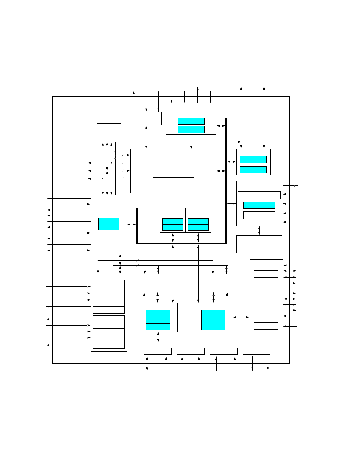
Figure 1. DSP16210 Block Diagram..................................................................................................................10
➤
Figure 2. DSP16000 Core Block Diagram.........................................................................................................16
➤
Figure 3. INT[3:0] and TRAP Timing .................................................................................................................24
➤
Figure 4. Interleaved Internal DPRAM...............................................................................................................25
➤
Figure 5. X-Memory Space Memory Map .........................................................................................................25
➤
Figure 6. Y-Memory Space Memory Maps........................................................................................................26
➤
Figure 7. Input Control Signal Conditioning.......................................................................................................33
➤
Figure 8. Frame Sync Timing with ILEV = ISLEV = 0 and ISDLY = 1................................................................33
➤
Figure 9. Input Functional Timing......................................................................................................................33
➤
Figure 10. Input Demultiplexer (
➤
Figure 11. Serial Input Clocking Example ...........................................................................................................35
➤
Figure 12. Output Control Signal Conditioning....................................................................................................37
➤
Figure 13. Output Functional Timing...................................................................................................................37
➤
Figure 14. Output Multiplexer (
➤
Figure 15. Serial Output Clocking Example.........................................................................................................40
➤
Figure 16. Modular I/O Units ...............................................................................................................................42
➤
Figure 17. Input and Output Buffer Configuration in IORAM
➤
Figure 18. Clock Synthesizer (PLL) Block Diagram.............................................................................................56
➤
Figure 19. Internal Clock Selection and Disable Logic........................................................................................57
➤
Figure 20. Allowable States and State Changes of
➤
Figure 21. Power Management and Clock Distribution........................................................................................62
➤
Figure 22. Interpretation of the Instruction Set Summary Table..........................................................................70
➤
Figure 23. DSP16210 Program-Accessible Registers.........................................................................................87
➤
Figure 24. DSP16210 144-Pin TQFP Pin Diagram (Top View) ........................................................................116
➤
Figure 25. DSP16210 Pinout by Interface.........................................................................................................121
➤
OH
Figure 26. Plot of V
➤
Figure 27. Plot of V
➤
Figure 28. I/O Clock Timing Diagram ................................ ...... ....... ..................................................................141
➤
Figure 29. Powerup Reset and Device Reset Timing Diagram ........................................................................142
➤
Figure 30. Reset Synchronization Timing..........................................................................................................143
➤
Figure 31. JTAG I/O Timing Diagram .............................................. ...... ...... ....... ...... ....... ...... ....... ... ... ....... ...... ..144
➤
Figure 32. Interrupt and Trap Timing Diagram ................................................................................................145
➤
Figure 33. Write Outputs Followed by Read Inputs (
➤
Figure 34. Enable Transition Timing..................................................................................................................147
➤
Figure 35. External Memory Data Read Timing Diagram (No Delayed Enable) ..............................................148
➤
Figure 36. External Memory Data Read Timing Diagram (Delayed Enable) ....................................................149
➤
Figure 37. External Memory Data Write Timing Diagram (DENB2 = 0, DENB1 = 0, DENB0 = 0)....................150
➤
Figure 38. External Memory Data Write Timing Diagram (DENB2 = 0, DENB1 = 1, DENB0 = 0)....................151
➤
Figure 39. READY Extended Read Cycle Timing..............................................................................................152
➤
Figure 40. PHIF16
➤
Figure 41. PHIF16
➤
Figure 42. PHIF16
➤
Figure 43. PHIF16
➤
Figure 44. PHIF16
➤
Figure 45. PIBF and POBE Reset Timing Diagram ..........................................................................................160
➤
Figure 46. POBE and PIBF Disable Timing Diagram........................................................................................160
➤
Figure 47. SSIO Passive Mode Input Timing Diagram .....................................................................................161
➤
Figure 48. SSIO Active Mode Input Timing Diagram ........................................................................................162
➤
Figure 49. SSIO Passive Mode Output Timing Diagram ..................................................................................163
➤
Figure 50. SSIO Active Mode Output Timing Diagram......................................................................................164
➤
Figure 51. Serial I/O Active Mode Clock Timing................................................................................................165
➤
vs. IOH Under Typical Operating Conditions ..................................................................136
OL
vs. IOL Under Typical Operating Conditions....................................................................136
Intel
Mode Signaling (Read and Write) Timing Diagram.....................................................153
Intel
Mode Signaling (Pulse Period and Flags) Timing Diagram ......................................155
Motorola
Motorola
Intel
or
IDMX
) and Register File Structure ....................................................................34
OMX
) and Register File Structure.......................................................................38
〈〈〈〈
〉〉〉〉
0, 1
.......................................................................45
pllc
Register Fields.............................................................59
cbit = IMMEDIATE; a1 = sbit
Mode Signaling (Read and Write) Timing Diagram..............................................156
Mode Signaling (Pulse Period and Flags) Timing Diagram .................................158
Motorola
Mode Signaling (Status Register Read) Timing Diagram .......................159
) Timing Characteristics....146
4
DRAFT COPY
Lucent Technologies Inc.
Page 5

Data Sheet
July 2000 D SP16210 Digital Signal Processor
List of Figures
(continued)
Figure Page
Figure 52. Simple Mode Input Timing Diagram.................................................................................................166
➤
Figure 53. Simple Mode Output Timing Diagram ..............................................................................................167
➤
Figure 54. Frame Mode Input Timing Diagram..................................................................................................168
➤
Figure 55. Frame Mode Output Timing Diagram...............................................................................................169
➤
Lucent Technologies Inc.
LUCENT TECHNOLOGIES—PROPRIETARY
Use pursuant to Company Instructions
5
Page 6

Data Sheet
DSP16210 Digital Signal Processor July 2000
List of Tables
Tables Page
Table 1. DSP16210 Block Diagram Legend.................................................................................................... 11
➤
Table 2. DSP16000 Core Block Diagram Legend........................................................................................... 17
➤
Table 3. State of Device Output and Bidirectional Pins During and After Reset............................................. 19
➤
Table 4. Interrupt and User Trap Vector Table................................................................................................ 21
➤
Table 5. Interrupt Control 0 and 1 (
➤
Table 6. Interrupt Status (
➤
Table 7. Interrupt Request Clearing Latency................................................................................................... 23
➤
Table 8. Access Time and Wait-States ........................................................................................................... 28
➤
Table 9. Wait-States........................................................................................................................................ 31
➤
Table 10. ESIO Memory Map (Input Section) ................................................................................................... 32
➤
Table 11. Input Channel Sta rt Bit Registers...................................................................................... ................ 35
➤
Table 12. ESIO Memory Map (Output Section)................................................................................................. 36
➤
Table 13. Output Channel Start Bit Registers ................................................................................................... 39
➤
Table 14. ESIO Interrupts.................................................................................................................................. 41
➤
Table 15. Instructions for Programming MIOU Registers.................................................................................. 42
➤
Table 16. MIOU〈0,1〉 16-Bit Directly Program-Accessible Registers................................................................. 43
➤
Table 17. MIOU Write-Only Command-Accessible Registers........................................................................... 43
➤
Table 18. MIOU〈0,1〉 Command (
➤
Table 19. Effect of Reset on MIOU Interrupts and Registers............................................................................ 44
➤
Table 20. MIOU Interrupts................................................................................................................................. 46
➤
Table 21. MIOU Command Latencies............................................................................................................... 48
➤
Table 22. PHIF16 Output Function.................................................................................................................... 51
➤
Table 23. PHIF16 Input Function ...................................................................................................................... 51
➤
Table 24. PHIF16 Status (
➤
Table 25. BIO Operations.................................................................................................................................. 52
➤
Table 26. BIO Flags .......................................................................................................................................... 52
➤
Table 27. JTAG Boundary-Scan Register......................................................................................................... 55
➤
Table 28. Clock Source Selection..................................................................................................................... 56
➤
Table 29.
➤
Table 30. Example Calculation of M and N....................................................................................................... 60
➤
Table 31. DSP16210 Instruction Groups........................................................................................................... 69
➤
Table 32. Instruction Set Summary................................................................................................................... 71
➤
Table 33. Notation Conventions for Instruction Set Descriptions...................................................................... 77
➤
Table 34. Overall Replacement Table............................................................................................................... 78
➤
Table 35. F1 Instruction Syntax......................................................................................................................... 81
➤
Table 36. F1E Function Statement Syntax........................................................................................................ 83
➤
Table 37. DSP16210 Conditional Mnemonics................................................................................................... 85
➤
Table 38. Program-Accessible Registers by Type, Listed Alphabetically ......................................................... 88
➤
Table 39. ESIO Memory-Mapped Registers ..................................................................................................... 90
➤
Table 40. MIOU-Accessible Registers .............................................................................................................. 90
➤
Table 41. DMA-Accessible Registers................................................................................................................ 90
➤
Table 42.
➤
Table 43.
➤
Table 44.
➤
Table 45.
➤
Table 46.
➤
Table 47.
➤
Table 48.
➤
Table 49.
➤
Table 50.
➤
Table 51.ID (JTAG Identification) Register....................................................................................................... 97
➤
pllc
Field Values Nbits[2:0] and Mbits[2:0]........................................................................................ 58
alf
Register........................................................................................................................................ 91
auc0
(Arithmetic Unit Control 0) Register ......................................................................................... 92
auc1
(Arithmetic Unit Control 1) Register ......................................................................................... 93
cbit
(BIO Control) Register ............................................................................................................... 94
cstate
ICR
ICSB
ICSL
ICVV
(Cache State) Register .......................................................................................................... 94
(ESIO Input Control) Register.................................................................................................... 95
0—7
〈〈〈〈
0—1
〈〈〈〈
(ESIO Input Channel Valid Vector) Register............................................................................ 96
ins
PSTAT
〉〉〉〉
(ESIO Input Channel Start Bit) Registers...................................................................... 96
〉〉〉〉
(ESIO Input Channel Sample Length) Registers........................................................... 96
inc0, inc1
) Register........................................................................................................... 22
mcmd
) Register ..................................................................................................... 51
) Registers ............................................................................... 22
0,1
〈〈〈〈
〉〉〉〉
) Register.................................................................................... 44
6
DRAFT COPY
Lucent Technologies Inc.
Page 7

Data Sheet
July 2000 D SP16210 Digital Signal Processor
List of Tables
(continued)
Tables Page
0—1
Table 52.
➤
Table 53.
➤
Table 54.
➤
Table 55.
➤
Table 56.
➤
Table 57.
➤
Table 58.
➤
Table 59.
➤
Table 60.
➤
Table 61.
➤
Table 62.
➤
Table 63.
➤
Table 64.
➤
Table 65.
➤
Table 66.
➤
Table 67.
➤
Table 68.
➤
Table 69.
➤
Table 70.
➤
Table 71.
➤
Table 72.
➤
Table 73.
➤
Table 74. Core Register States After Reset—40-bit Registers ....................................................................... 113
➤
Table 75. Core Register States After Reset—32-bit Registers ....................................................................... 113
➤
Table 76. Core Register States After Reset—20-bit Registers ....................................................................... 113
➤
Table 77. Core Register States After Reset—16-bit Registers ....................................................................... 114
➤
Table 78. Peripheral (Off-Core) Register States After Reset.......................................................................... 114
➤
Table 79. RB Field.. ......................................................................................................................................... 115
➤
Table 80. Pin Descriptions .............................................................................................................................. 117
➤
Table 81. Command Encoding for Boot Routines........................................................................................... 127
➤
Table 82. Absolute Maximum Ratings............................................................................................................. 133
➤
Table 83. Recommended Operating Conditions ............................................................................................. 133
➤
Table 84. Package Thermal Considerations ................................................................................................... 134
➤
Table 85. Electrical Characteristics and Requirements................................................................................... 135
➤
Table 86. Power Dissipation............................................................................................................................ 137
➤
Table 87. Frequency Ranges for PLL Output.................................................................................................. 139
➤
Table 88. PLL Loop Filter Settings and Lock-In Time..................................................................................... 139
➤
Table 89. Wake-Up Latency............................................................................................................................ 140
➤
Table 90. Timing Requirements for Input Clock.............................................................................................. 141
➤
Table 91. Timing Characteristics for Input Clock and Output Clock................................................................ 141
➤
Table 92. Timing Requirements for Powerup Reset and Device Reset.......................................................... 142
➤
Table 93. Timing Characteristics for Powerup Reset and Device Reset......................................................... 142
➤
Table 94. Timing Requirements for Reset Synchronization Timing ................................................................ 143
➤
Table 95. Timing Requirements for JTAG I/O................................................................................................. 144
➤
Table 96. Timing Characteristics for JTAG I/O................................................................................................ 144
➤
Table 97. Timing Requirements for Interrupt and Trap ................................................................................... 145
➤
Table 98. Timing Characteristics for Interrupt and Trap.................................................................................. 145
➤
Table 99. Timing Requirements for BIO Input Read....................................................................................... 146
➤
Table 100.Timing Characteristics for BIO Output............................................................................................. 146
➤
Table 101.Timing Characteristics for Memory Enables and RWN................................................................... 147
➤
Table 102.Timing Characteristics for External Memory Access (DENB = 0) ....................................................148
➤
inc
ins
ioc
mcmd
miwp
morp
mwait
OCR
OCSB
OCSL
OCVV (
PHIFC
pllc
powerc
PSTAT
psw0
psw1
sbit
SSIOC
timer〈0,1
timer〈0,1〉c
vsw
(
〈〈〈〈
〉〉〉〉
Interrupt Control) Registers ............................................................................................. 97
(Interrupt Status) Register........................................................................................................... 98
(I/O Configuration) Register........................................................................................................ 99
0—1
〈〈〈〈
〉〉〉〉
(MIOU
0—1
〈〈〈〈
〉〉〉〉
(MIOU
0—1
〈〈〈〈
〉〉〉〉
(MIOU
(EMI Configuration) Register................................................................................................ 101
(ESIO Output Control) Register.............................................................................................. 102
0—7
〈〈〈〈
〉〉〉〉
(ESIO Output Channel Start Bit) Registers ............................................................... 103
0—1
〈〈〈〈
〉〉〉〉
(ESIO Output Channel Sample Length) Registers .................................................... 103
ESIO Output Channel Valid Vector) Register ..................................................................... 103
(PHIF16 Control) Register................................................................................................... 104
(Phase-Lock Loop Control) Register........................................................................................ 105
(Power Control) Register ................................................................................................... 106
(PHIF16 Status) Register ................................................................................................... 106
(Processor Status Word 0) Register...................................................................................... 107
(Processor Status Word 1) Register...................................................................................... 108
(BIO Status/Control) Register.................................................................................................. 109
(SSIO Control) Register ...................................................................................................... 110
〉
(TIMER〈0,1〉 Running Count) Register........................................................................... 111
(TIMER〈0,1〉 Control) Register ..................................................................................... 111
(Viterbi Support Word) Register .............................................................................................. 112
〈〈〈〈
〉〉〉〉
0—1
Command) Registers .......................................................................... 100
〈〈〈〈
〉〉〉〉
0—1
IORAM Input Write Pointer) Registers.................................................. 100
〈〈〈〈
〉〉〉〉
0—1
IORAM Output Read Pointer) Registers............................................... 101
Lucent Technologies Inc.
DRAFT COPY
7
Page 8

Data Sheet
DSP16210 Digital Signal Processor July 2000
List of Tables
(continued)
Tables Page
Table 103.Timing Requirements for External Memory Read (DENB = 0).........................................................148
➤
Table 104.Timing Characteristics for External Memory Access (DENB = 1) ....................................................149
➤
Table 105.Timing Requirements for External Memory Read (DENB = 1).........................................................149
➤
Table 106.Timing Characteristics for External Memory Data Write (RWNADV = 0, DENB = 0)...................... 150
➤
Table 107.Timing Characteristics for External Memory Data Write (RWNADV = 1, DENB = 1)...................... 151
➤
Table 108.Timing Requirements for READY Extended Read Cycle Timing.................................................... 152
➤
Intel
Table 109.Timing Requirements for PHIF16
➤
Table 110.Timing Characteristics for PHIF16
➤
Table 111.Timing Requirements for PHIF16
➤
Table 112.Timing Characteristics for PHIF16
➤
Table 113.Timing Requirements for PHIF16
➤
Table 114.Timing Characteristics for PHIF16
➤
Table 115.Timing Characteristics for PHIF16
➤
Table 116.Timing Requirements for PHIF16
➤
Intel
Intel
and
and
Table 117.Timing Requirements for
➤
Table 118.Timing Characteristics for
➤
Table 119.PHIF16 Timing Characteristics for PIBF and POBE Reset............................................................. 160
➤
Table 120.PHIF16 Timing Characteristics for POBE and PIBF Disable .......................................................... 160
➤
Table 121.Timing Requirements for Serial Inputs (Passive Mode).................................................................. 161
➤
Table 122.Timing Characteristics for Serial Outputs (Passive Mode).............................................................. 161
➤
Table 123.Timing Requirements for Serial Inputs (Active Mode)..................................................................... 162
➤
Table 124.Timing Characteristics for Serial Outputs (Active Mode) ................................................................ 162
➤
Table 125.Timing Requirements for Serial Inputs (Passive Mode).................................................................. 163
➤
Table 126.Timing Characteristics for Serial Outputs (Passive Mode).............................................................. 163
➤
Table 127.Timing Characteristics for Serial Output (Active Mode) .................................................................. 164
➤
Table 128.Timing Characteristics for Signal Generation (Active Mode) .......................................................... 165
➤
Table 129.Timing Requirements for ESIO Simple Input Mode ........................................................................ 166
➤
Table 130.Timing Characteristics for ESIO Simple Input Mode....................................................................... 166
➤
Table 131.Timing Requirements for ESIO Simple Output Mode ..................................................................... 167
➤
Table 132.Timing Characteristics for ESIO Simple Output Mode.................................................................... 167
➤
Table 133.Timing Requirements for ESIO Frame Input Mode......................................................................... 168
➤
Table 134.Timing Characteristics for ESIO Frame Input Mode ....................................................................... 168
➤
Table 135.Timing Requirements for ESIO Frame Output Mode ...................................................................... 169
➤
Table 136.Timing Characteristics for ESIO Frame Output Mode..................................................................... 169
➤
Mode Signaling (Read and Write)...................................... 153
Intel
Mode Signaling (Read and Write) .................................... 154
Intel
Mode Signaling (Pulse Period and Flags).......................... 155
Intel
Mode Signaling (Pulse Period and Flags)........................ 155
Motorola
Motorola
Motorola
Motorola
Motorola
Mode Signaling (Read and Write)............................... 156
Mode Signaling (Pulse Period and Flags) .................. 158
Motorola
Mode Signaling (Read and Write)............................. 157
Mode Signaling (Pulse Period and Flags)................. 158
Mode Signaling (Status Register Read).................... 159
Mode Signaling (Status Register Read) .................. 159
8
DRAFT COPY
Lucent Technologies Inc.
Page 9

Data Sheet
July 2000 D SP16210 Digital Signal Processor
Notation Conventions
The following notation conventions apply to this data
sheet:
lower-case Registers that are directly writable or
readable by DSP16210 core instructions are lower-case.
UPPER-CASE Device flags, I/O pins, and registers
that are not directly writable or readable by DSP16210 core instructions
are upper-case.
boldface
italics
courier
[ ] Square brackets enclose a range of
〈〉
Register names and DSP16210 core
instructions are printed in boldface
when used in text descriptions.
Documentation varia ble s that are replaced are printed in italics.
DSP16210 program examples are
printed in courier font.
numbers that represents multiple bits in
a single register or bus. The range of
numbers is delimited by a colon. For
example,
program-accessible
Angle brackets enclose a list of items
delimited by commas or a range of
items delimited by a dash (—), one of
which is selected if used in an
instruction. For example,
represents the eight memory-mapped
registers
and the general instruction
aTE
a0h = timer0
ioc
ICSB0, ICSB1
h,l〉=RB
〈
[7:5] are bits 7—5 of the
ioc
register.
ICSB
0—7
〈
ICSB7
, ...,
can be replaced with
.
〉
,
Hardware Architecture
The DSP16210 device is a 16-bit fixed-point programmable digital signal processor (DSP). The DSP16210
consists of a DSP16000 core together with on-chip
memory and peripherals. Advanced architectural features with an expanded instruction set deliver a dramatic increase in performance for signal coding
algorithms. This increase in performance together with
an efficient design implementation results in an
extremely cost- and power-efficient solution for wireless
and multimedia applications.
DSP16210 Architectural Overview
Figure 1 on page 10 shows a block diagram of the
DSP16210. The following blocks make up this device.
DSP16000 Core
The DSP16000 core is the signal-processing engine of
the DSP16210. It is a modified Harvard architecture
with separate sets of buses for the instruction/coefficient (X-memory) and data (Y-memory) spaces. Each
set of buses has 20 bits of address and 32 bits of data.
The core contains data and address arithmetic units
and control for on-chip memory and peripherals.
Clock Synthesizer (PLL)
The DSP16210 exits device reset with an input clock
(CKI) as th e source for the internal clock (CLK). An onchip clock synthesizer (PLL) that runs at a frequency
multiple of CKI can also be used to generate CLK. The
clock synthesizer is deselected and powered down on
reset. For low-power operation, an internally generated
slow clock can drive the DSP.
The clock synthesizer and other programmable clock
sources are discussed in Clock Synthesis beginning on
page 56. The use of these programmable clock
sources for power management is discussed in Power
Management beginning on page 61.
Dual-Port RAM (DPRAM)
This block contains 60 banks (banks 1—60) of zero
wait-state memory. Each bank consists of 1K 16-bit
words and has separate address and data ports to the
instruction/coefficient (X-memory) and data (Y-memory) spaces. DPRAM is organized into even and odd
interleaved banks where each ev en/odd pair is a 32-bit
wide module (see Figure 4 on page 25 for details).
Placing instructions and Y-memory data in the same 2K
module of DPRAM is not supported and may cause
undefined results.
A program can be downloaded from slow off-chip memory into DPRAM, and then executed without waitstates. DPRAM is also useful for improving convolution
performance in cases where the coefficients are adaptive. Since DPRAM can be downloaded through the
JTAG port, full-speed remote in-circuit emulation is
possible.
Lucent Technologies Inc.
DRAFT COPY
9
Page 10
Data Sheet
DSP16210 Digital Signal Processor July 2000
Hardware Architecture
(continued)
DSP16210 Architectural Overview
IROM
8K x 16
32
ioc
mwait
ESIO
〈
0—15
ICR
ICVV
OCR
20
32
20
EDBEAB
‡
〉
‡
〉
‡
〉
‡
‡
‡
〉
‡
〉
‡
〉
‡
‡
ERAMLO
READY
ERAMHI
EROM
ERAM
EXM
RWN
AB[15:0]
DB[15:0]
EDI
EIFS
EIBC
EIBF
EDO
EOFS
EOBC
EOEB
EOBE
DPRAM
60K x 16
BANKS 1—60
EXTERNAL
MEMORY
INTERFACE
IO
IDMX
ICSB〈0—7
ICSL〈0—1
OMX〈0—15
OCSB〈0—7
OCSL〈0—1
OCVV
(continued)
INT[3:0]
TRAPIACK
INTERRUPT
LOGIC
VEC[3:0]
XDB
XAB
YDB
YAB
10
16
IORAM0
1K x 16
MIOU0
mcmd0
miwp0
morp0
PHIFC
STOP
RSTB
CLOCK SELECTION
AND SYNTHESIS (PLL)
powerc
DSP16000 CORE
TIMER0
timer0c
timer0
‡
PSTAT
CKO
pllc
CLK
TIMER1
timer1c
timer1
§
CKI
IDB
IORAM1
1K x 16
MIOU1
mcmd1
miwp1
morp1
PHIF16
PDX(in)
IOBIT[7:4]/
†
VEC[3:0]
BIO
sbit
cbit
BOUNDARY SCAN
‡
PDX(out)
IOBIT[3:0]
JTAG
jiob
§
ID
HDS
SSIO
SSDX(in)
SSDX(out)
SSIOC
‡
TDO
§
‡
‡
‡
TDI
TCK
TMS
TRST
DI
ICK
ILD
IBF
DO
OCK
OLD
OBE
DOEN
SYNC
PB[15:0] PIDS PODS PCSN PSTATPBSEL
† VEC0 corresponds to IOBIT7, VEC1 corresponds to IOBIT6, VEC2 corresponds to IOBIT5, and VEC3 corresponds to IOBIT4.
‡ These registers are not directly program accessible.
§ These registers are accessible through pins only.
Figure 1. DSP16210 Block Diagram
10
DRAFT COPY
PIBFPOBE
Lucent Technologies Inc.
Page 11

Data Sheet
July 2000 D SP16210 Digital Signal Processor
Hardware Architecture
DSP16210 Architectural Overview
Table 1. DSP16210 Block Diagram Legend
Symbol Description
BIO Bit I/O Unit
cbit
CLK Internal Clock Signal
DPRAM Dual-por t Rand om- A cces s Mem ory
EAB EMI Address Bus
EDB EMI Data Bus
ESIO Enhanced Serial I/O Unit
HDS Hardware Development System Unit
ICR
ICSB
0—7
〈
ICSL
0—1
〈
ICVV
IDMX
0—15
〈
ID
IDB Internal Data Bus
ioc
IORAM0 Internal I/O RAM 0: Shared with MIOU0
IORAM1 Internal I/O RAM 1: Shared with MIOU1
IROM Internal Boot Read-Only Memory
jiob
JTAG JTAG Test Port
MIOU0 Modular I/O Unit 0: Controls PHIF16
mcmd0
miwp0
morp0
MIOU1 Modular I/O Unit 1: Controls SSIO
mcmd1
miwp1
morp1
mwait
OCR
OCSB
OCSL
OMX
0—7
〈
0—1
〈
OCVV
0—15
〈
PDX
(in) PHIF16 Input Register; Readable by MIOU0
PDX
(out) PHIF16 Output Register; Writable by MIOU0
PHIF16 16-bit Parallel Host Interface
PHIFC
PLL Phase-Lock Loop
pllc
BIO Control Register
ESIO Input Control Register
〉
ESIO Input Channel Start Bit Registers
〉
ESIO Input Channel Sample Length Registers
ESIO Input Channel Valid Vector Register
〉
ESIO Input Demultiplexer Registers
JTAG Device Identification Register
I/O Configuration Register
JTAG Test Register
MIOU0 Command Register
MIOU0 IORAM0 Input Write Pointer
MIOU0 IORAM0 Output Read Pointer
MIOU1 Command Register
MIOU1 IORAM1 Input Write Pointer
MIOU1 IORAM1 Output Read Pointer
EMI Configuration Register
ESIO Output Control Register
〉
ESIO Output Channel Start Bit Registers
〉
ESIO Output Channel Sample Length Registers
ESIO Output Channel Valid Vector Register
〉
ESIO Output Multiplexer Registers
PHIF16 Control Register: Programmed Through MIOU0
Phase-Lock Loop Control Register
(continued)
(continued)
Lucent Technologies Inc.
DRAFT COPY
11
Page 12

Data Sheet
DSP16210 Digital S ignal Processor July 2000
Hardware Architecture
DSP16210 Architectural Overview
Table 1. DSP16210 Block Diagram Legend
Symbol Description
powerc
PSTAT
sbit
SSDX
(in) SSIO Input Register; Readable by MIOU1
SSDX
(out) SSIO Output Register; Writable by MIOU1
SSIO Simple Serial I/O Unit
SSIOC
TIMER0 Programmable Timer 0
timer0
timer0c
TIMER1 Programmable Timer 1
timer1
timer1c
XAB X-Memory Space Address Bus
XDB X-Memory Space Data Bus
YAB Y-Memory Space Address Bus
YDB Y-Memory Space Data Bus
Power Control Register
PHIF16 Status Register
BIO Status/Control Regi st er
SSIO Control Register: Programmed Through MIOU1
Timer Running Count Register for TIMER0
Timer Control Register for TIMER0
Timer Running Count Register for TIMER1
Timer Control Register for TIMER1
(continued)
(continued)
(continued)
Internal Boot ROM (IROM)
The DSP16210 includes a boot ROM that contains
hardware development code and boot routines. The
boot routines are available for use by the programmer
and are detailed in DSP16210 Boot Routines begin-
ning on page 126.
IORAM and Modular I/O Units (MIOUs)
IORAM storage consists of two 1 Kword banks of memory , IORAM0 and IORAM1. Each IORAM bank has two
16-bit data and two 10-bit address ports; an IORAM
bank can be shared with the core and a modular I/O
unit (MIOU) to implement a DMA-based I/O system.
IORAM supports concurrent core execution and MIOU
I/O processing.
MIOU0 (controls PHIF16) is attached to IORAM0;
MIOU1 (controls SSIO) is attached to IORAM1. Portions of IORAM not dedicated to I/O processing can be
used as general-purpose data storage.
Placing instructions and Y-memory data in the same
IORAM is not supported and may cause undefined
results.
The IORAMs and MIOUs are described in detail in
Modular I/O Units (MIOUs) beginning on page 42.
External Memory Interface (EMI)
The EMI connects the DSP16210 to external memory
and I/O devices. It multiplexes the two sets of core
buses (X and Y) onto a single set of external buses—a
16-bit address bus (AB[15:0]) and 16-bit data bus
(DB[15:0]). These external buses can access external
RAM (ERAMHI/ERAMLO), external ROM (EROM), and
memory-mapped I/O space (IO).
The EMI also manages the on-chip IORAM and ESIO
storage. It multiplexes the two sets of core buses onto a
single set of internal buses—a 10-bit address bus
(EAB[9:0]) and 16-bit data bus (EDB[15:0])—to interface to the IORAMs and ESIO memory-mapped registers.
Instructions can transparently reference external memory, IORAM, and ESIO storage from either set of core
buses. The EMI automatically translates a single 32-bit
access into two 16-bit accesses and vice versa.
The EMI is described in detail in External Memory
Interface (EMI) beginning on page 27.
12
DRAFT COPY
Lucent Technologies Inc.
Page 13

Data Sheet
July 2000 D SP16210 Digital Signal Processor
Hardware Architecture
DSP16210 Architectural Overview
Bit I/O (BIO) Unit
The BIO unit provides convenient and efficient monitoring and control of eight individually configurable pins
(IOBIT[7:0]). When configured as outputs, the pins can
be individually set, cleared, or toggled. When configured as inputs, individual pins or combinations of pins
can be tested for patterns. Flags returned by the BIO
are testable by conditional instructions. See Bit
Input/Output Unit (BIO) beginning on page 52 for more
details.
Enhanced Serial I/O (ESIO) Unit
The ESIO is a programmable, hardware-managed,
passive, double-buffered full-duplex serial input/output
port designed to support glueless multichannel I/O processing on a TDM (time-division multiplex) highway. In
simple mode, the ESIO supports data rates of up to
26 Mbits/s for a single channel with either 8-bit or 16-bit
data lengths. In frame mode, the ESIO processes up to
16 logical TDM channels with a data rate of up to
8.192 Mbits/s. For more information on the ESIO, see
Enhanced Serial I/O (ESIO) Unit beginning on
page 32.
Simple Serial I/O (SSIO) Unit
The SSIO unit offers a full-duplex, double-buffered
external channel that operates at up to 26 Mbits/s.
Commercially available codecs and time-division multiplex channels can be interfaced to the SSIO with few, if
any, additional components.
The SSIO is a DMA peripheral managed by MIOU1.
See Simple Serial I/O (SSIO) Unit beginning on
page 49 for more information.
Parallel Host Interface (PHIF16)
The PHIF16 is a DMA peripheral managed by MIOU0.
It is a passive 16-bit parallel port that can be configured
to interface to either an 8- or 16-bit external bus containing other Lucent Technologies DSPs, microprocessors, or off-chip I/O devices. The PHIF16 port supports
either
Motorola
or
Intel
protocols.
(continued)
(continued)
or low byte access; in 8-bit mode, only the low byte is
accessed.
Additional software-programmable features allow for a
glueless host interface to microprocessors (see Parallel
Host Interface (PHIF16) beginning on page 49).
Timers
The two timers can be used to provide an interrupt,
either single or repetitive, at the expiration of a programmed interval. More than nine orders of magnitude
of interval selection are provided. The timers can be
stopped and restarted at any time under program control. See Timers beginning on page 53 for more information.
Test Access Port (JTAG)
The DSP16210 provides a test access port that conforms to
boundary scan test access and also controls the Hardware Development System (HDS). See JTAG Test Port
beginning on page 54 for details.
Hardware Development System (HDS)
The HDS is an on-chip hardware module available for
debugging assembly-language programs that execute
on the DSP16000 core in real-time. The main capability
of the HDS is in allowing controlled visibility into the
core’s state during program execution. The HDS is
enhanced with powerful debugging capabilities such as
complex breakpointing conditions, multiple
data/address watchpoint registers, and an intelligent
trace mechanism for recording discontinuities. See
Hardware Development System (HDS) beginning on
page 54 for details.
Pin Multiplexing
The upper four BIO pins (IOBIT[7:4]) are multiplexed
with the vectored interrupt identification pins
(VEC[3:0]). Specifically, VEC0 is multiplexed with
IOBIT7, VEC1 with IOBIT6, VEC2 with IOBIT5, and
VEC3 with IOBIT4. VEC[3:0] are connected to the
package pins and IOBIT[7:4] are disconnected immediately after device reset. To select IOBIT[7:4] to be connected to these pins, the program must set EBIO (bit 8
of the
IEEE
ioc
register).
1149.1 (JTAG). The JTAG port provides
When operating in the 16-bit external bus configuration, PHIF16 can be programmed to swap high and low
bytes. When operating in 8-bit external bus configuration, PHIF16 is accessed in either an 8-bit or 16-bit logical mode. In 16-bit mode, the host selects either a high
Lucent Technologies Inc.
DRAFT COPY
13
Page 14

Data Sheet
DSP16210 Digital Signal Processor July 2000
Hardware Architecture
(continued)
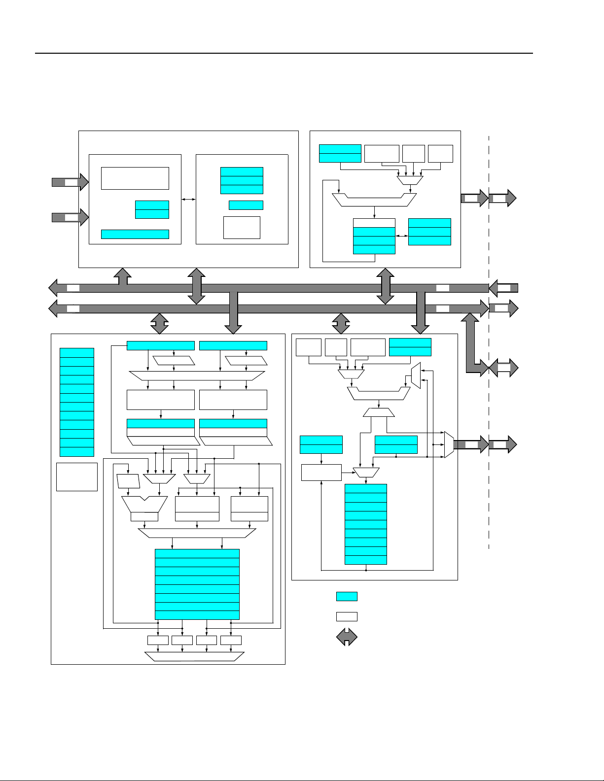
DSP16000 Core Architectural Overview
See the
mation Manual for a complete description of the
DSP16000 core. Figure2 on page16 shows a block
diagram of the core that consists of four major blocks:
System Control and Cache (SYS), Data Arithmetic Unit
(DAU), Y-Memory Space Address Arithmetic Unit
(YAAU), and X-Memory Space Address Arithmetic Unit
(XAAU). Bits within the
figure the DAU mode-controlled operations.
System Control and Cache (SYS)
This section consists of the control block and the
cache.
The control block provides overall system coordination
that is mostly invisible to the user. The control block
includes an instruction decoder and sequencer, a
pseudorandom sequence generator (PSG), an interrupt and trap handler, a wait-state generator, and lowpower standby mode control logic. An interrupt and trap
handler provides a user-locatable vector table and
three levels of user-assigned interrupt priority.
SYS contains the
that contains AWAIT, a power-saving standby mode
bit, and peripheral flags. The
are 20-bit interrupt control registers, and
interrupt status register.
Programs use the instruction cache to store and execute repetitive operations such as those found in an
FIR or IIR filter section. The cache can contain up to 31
16-bit and 32-bit instructions. The code in the cache
can repeat up to 2
head. Operations in the cache that require a coefficient
access execute at twice the normal rate because the
XAAU and its associated bus are not needed for fetching instructions. The cache greatly reduces the need
for writing in-line repetitive code and, therefore,
reduces instruction/coefficient memory size requirements. In addition, the use of cache reduces power
consumption because it eliminates memory accesses
for instruction fetches.
The
cstate
The 32-bit
instruction following the loop instruction in Xmemory.The cache provides a convenient, low-overhead looping structure that is interruptible, savable, and
restorable. The cache is addressable in both the X and
DSP16000 Digital Signal Processor Core
auc0
alf
register, which is a 16-bit register
16
– 1 times without looping over-
cloop
register controls the cache loop count. The
register contains the current state of the cache.
csave
register holds the opcode of the
and
inc0
auc1
registers con-
inc1
and
ins
registers
is a 20-bit
Info r -
Y memory spaces. An interrupt or trap handling routine
can save and restore
contents of the cache.
Data Arithmetic Unit (DAU)
The DAU is a power-efficient, dual-MAC (multiply/accumulate) parallel-pipelined structure that is tailored to
communications applications. It can perform two double-word (32-bit) fetches, two multiplications, and two
accumulations in a single instruction cycle. The dualMAC parallel pipeline begins with two 32-bit registers, x
and y. The pipeline treats the 32-bit registers as four
16-bit signed registers if used as input to two signed
16-bitx16-bit multipliers. Each multiplier produces a
full 32-bit result stored into registers p0 and p1. The
DAU can direct the output of each multiplier to a 40-bit
ALU or a 40-bit 3-input ADDER.The ALU and ADDER
results are each stored in one of eight 40-bit accumulators, a0 through a7. The ALU includes an ACS
(add/compare/select) function for Viterbi decoding. The
DAU can direct the output of each accumulator to the
ALU/ACS, the ADDER, or a 40-bit BMU (bit manipulation unit).
The ALU implements addition, subtraction, and various
logical operations. To support Viterbi decoding, the
ALU has a split mode in which it computes two simultaneous 16-bit additions or subtractions. This mode,
available in a specialized dual-MAC instruction, is used
to compute the distance between a received symbol
and its estimate.
The ACS provides the add/compare/select function
required for Viterbi decoding. This unit provides flags to
the traceback encoder for implementing mode-controlled side-effects for ACS operations. The source
operands for the ACS are any two accumulators, and
results are written back to one of the source accumulators.
The BMU implements barrel-shift, bit-field insertion, bitfield extraction, exponent extraction, normalization, and
accumulator shuffling operations.
auxiliary registers whose main function is to control
BMU operations.
The user can enable overflow saturation to affect the
multiplier output and the results of the three arithmetic
units. Overflow saturation can also affect an accumulator value as it is transferred to memory or other register.
These features accommodate various speech coding
standards such as GSM-FR, GSM-HR, and GSM-EFR.
Shifting in the arithmetic pipeline occurs at several
stages to accommodate various standards for mixedand double-precision multiplications.
cloop, cstate, csave
ar0
through
, and the
ar3
are
14
DRAFT COPY
Lucent Technologies Inc.
Page 15

Data Sheet
July 2000 D SP16210 Digital Signal Processor
Hardware Architecture
(continued)
DSP16000 Core Architectural Overview
(continued)
and
and
auc0
auc1
psw1
ar1
auxil-
re1
and
Informa-
,
The DAU contains control and status registers
auc1, psw0, psw1, vsw
The arithmetic unit control registers
select or deselect various modes of DAU operation.
These modes include scaling of the products, saturation on overflow, feedback to the x and y registers fr om
accumulators a6 and a7, simultaneous loading of x and
y
registers with the same value (used for single-cycle
squaring), and clearing the low half of registers when
loading the high half to facilitate fixed-point operations.
The processor status word registers
contain flags set by ALU/ACS, ADDER, or BMU operations. They also include information on the current status of the interrupt controller.
vsw
The
with the traceback encoder. The traceback encoder is a
specialized block for accelerating Viterbi decoding. It
performs mode-controlled side-effects for three MAC
instruction group compare functions:
and
side-effects allow the DAU to store, with no overhead,
state information necessary for traceback decoding.
Side-effects use the c1 counter, the
iary registers, and bits 1 and 0 of
The
used to count events such as the number of times the
program has executed a sequence of code. The c2
register is a holding register for counter c1. Conditional
instructions control these counters and provide a convenient method of program looping.
Y-Memory Space Address Arithmetic Unit (YAAU)
The YAAU supports high-speed, register-indirect, data
memory addressing and postincrementing of the
address register. Eight 20-bit pointer registers (r0—r7)
store read or write addresses for the Y-memory space.
Two sets of 20-bit registers (
define the upper and lower boundaries of two zerooverhead circular buffers for efficient filter implementations. The j and k registers are two 20-bit signed registers that are used to hold user-defined postincrement
values for r0—r7. Fixed increments of +1, –1, 0, +2,
and –2 are also available. (P ostincrement options 0 and
–2 are not available for some specialized transfers. See
the
tion Manual for details.)
register is the Viterbi support word associated
cmp2( )
c1
and
. The
c0
counters are 16-bit signed reg is ter s
DSP16000 Digital Signal Processor Core
, and c0—c2.
auc0
psw0
cmp0( ), cmp1( )
vsw
register controls the modes. The
ar0
and
vsw
.
rb0
and
re0; rb1
The YAAU includes a 20-bit stack pointer (sp). The
data move group includes a set of stack instructions
that consists of push, pop, stack-relative, and pipelined
stack-relative operations. The addressing mode used
for the stack-relative instructions is register-plus-displacement indirect addressing (the displacement is
optional). The displacement is specified as either an
immediate value as part of the instruction or a value
stored in j or k. The YAAU computes the address by
adding the displacement to sp and leaves the contents
of sp unchanged. The data move group also includes
instructions with register-plus-displacement indirect
pt0
r6
and
addressing for the pointer registers r0—
sp
.
The data move group of instructions includes instructions for loading and storing any YAAU register from or
to memory or another core register. It also includes
instructions for loading any YAAU register with an
immediate value stored with the instruction. The
pointer arithmetic group of instructions allows adding of
an immediate value or the contents of the j or k register
to any YAAU pointer register and storing the result to
any YAAU register.
X-Memory Space Address Arithmetic Unit (XAAU)
,
The XAAU contains registers and an adder that control
the sequencing of instructions in the processor. The
program counter (PC) automatically increments
through the instruction space. The interrupt return register pi, the subroutine return register pr, and the trap
return register
return addresses that direct the return to main program
execution from interrupt service routines, subroutines,
and trap service routines, respectively. High-speed,
register-indirect, read-only memory addressing with
postincrementing is done with the
ters. The signed registers h and i are used to hold a
user-defined signed postincrement value. Fixed postincrement values of 0, +1, –1, +2, and –2 are also available. (Postincrement options 0 and –2 are available
only if the target of the data transfer is an accumulator
vector.
Core
)
The data move group of instructions includes instructions for loading and storing any XAAU register from or
to memory or another core register. It also includes
instructions for loading any XAAU register with an
immediate value stored with the instruction.
vbase
programs this register with the base address of the
interrupt and trap vector table.
See the DSP16000 Digital Signal Processor
Information Manual for details.)
is the 20-bit vector base offset register. The user
ptrap
are automatically loaded with
in addition to
pt1
regis-
Lucent Technologies Inc.
DRAFT COPY
15
Page 16
Data Sheet
DSP16210 Digital Signal Processor July 2000
Hardware Architecture
(continued)
DSP16000 Core Architectural Overview
SYS
XAB
(20)
YAB
DAU
auc0 (16)
auc0 (16)
auc1 (16)
auc1 (16)
psw0 (16)
psw0 (16)
psw1 (16)
psw1 (16)
(20)
XDB
(32)
IDB
(32)
vsw (16)
vsw (16)
c0 (16)
c0 (16)
c1 (16)
c1 (16)
c2 (16)
c2 (16)
ar0 (16)
ar0 (16)
ar1 (16)
ar1 (16)
ar2 (16)
ar2 (16)
ar3 (16)
ar3 (16)
CACHE
31 INSTRUCTIONS
cloop (16)
cloop (16)
cstate (16)
cstate (16)
csave (32)
csave (32)
y (32) x (32)
y (32) x (32)
SHIFT(0, –1) SHIFT(0, –1)
SWAP MUX
16 × 16 MULTIPLY 16 × 16 MULTIPL Y
p0 (32)
p0 (32)
SHIFT(2, 1, 0, –2)/SAT.
SHIFT(2, 1, 0, –2)/SAT.
SHIFT(0, –1)
CONTROL
ins (20)
ins (20)
inc0 (20)
inc0 (20)
inc1 (20)
inc1 (20)
alf (16)
alf (16)
PSG
p1 (32)
p1 (32)
SHIFT(2, 1, 0, –2)/SAT.
SHIFT(2, 1, 0, –2)/SAT.
SHIFT(0, –15, –16)
(continued)
DOUBLE
–2, 0, 2
re0 (20)
re0 (20)
re1 (20)
re1 (20)
h (20)
h (20)
i (20)
i (20)
SINGLE
–1, 0, 1
IMMEDIATE
VALUE
MUX
IMMEDIATE
VALUE
+
PC (20)
pt0 (20)
pt0 (20)
pt1 (20)
pt1 (20)
vbase (20)
vbase (20)
‡
+
DEMUX
†
rb0 (20)
rb0 (20)
rb1 (20)
rb1 (20)
SINGLE
–1, 0, 1
MUX
j (20)
j (20)
k (20)
k (20)
MUX
DOUBLE
–2, 0, 2
pi (20)
pi (20)
pr (20)
pr (20)
ptrap(20)
ptrap(20)
XAAU
XDB
(32)
IDB
(32)
YAAU
XAB
(20)
YAB YAB
MUX
(20) (20)
OFF-
CORE
TO
MEMORY
XAB
(20)
FROM
MEMORY
XDB
(32)
IDB
(32)
TO
PERIPH-
ERAL
YDB
(32)
TO/FROM
MEMORY
TO
MEMORY
TRACEBACK
ENCODER
SHIFT
(0, –14)
MUX
ALU/ACS ADDER BMU
SA T.
SA T.
SAT.
SAT.
MUX
SAT. SAT.
SAT. SAT.
SPLIT/MUX
a0 (40)
a0 (40)
a1 (40)
a1 (40)
a2 (40)
a2 (40)
a3 (40)
a3 (40)
a4 (40)
a4 (40)
a5 (40)
a5 (40)
a6 (40)
a6 (40)
a7 (40)
a7 (40)
MUX/EXTRACT
SAT.SAT. SA T.
SAT.SAT. SA T.
† Associated with PC-relative branch addressing.
‡ Associated with register-plus-displacement indirect addressing.
Figure 2. DSP16000 Core Block Diagram
16
COMPARE
DRAFT COPY
KEY:
MUX
r0 (20)
r0 (20)
r1 (20)
r1 (20)
r2 (20)
r2 (20)
r3 (20)
r3 (20)
r4 (20)
r4 (20)
r5 (20)
r5 (20)
r6 (20)
r6 (20)
r7 (20)
r7 (20)
sp (20)
sp (20)
PROGRAM-A C C ESSIBLE REGISTERS
MODE-CONTROLLED OPTIONS
BUSES
Lucent Technologies Inc.
Page 17

Data Sheet
July 2000 D SP16210 Digital Signal Processor
Hardware Architecture
DSP16000 Core Architectural Overview
Table 2. DSP16000 Core Block Diagram Legend
Symbol Name
16 x 16 MULTIPLY 16-bit x 16-bit Multiplier
a0—a7
ADDER 3-input 40-bit Adder/Subtractor
alf
ALU/ACS 40-bit Arithmetic Logic Unit and Add/Compare/Select Function—used in Viterbi decoding
ar0—ar3
auc0, auc1
BMU 40-bit Bit Manipulation Unit
c0, c1
c2
cloop
COMPARE Comparator
csave
cstate
DAU Data Arithmetic Unit
h
i
IDB Internal Data Bus
inc0, inc1
ins
j
k
MUX Multiplexer
p0, p1
PC
pi
pr
PSG Pseudorandom Sequence Generator
psw0, psw1
pt0, pt1
ptrap
r0—r7
rb0, rb1
re0, re1
SAT Saturation
SHIFT Shifting Operation
sp
SPLIT/MUX Split/Multiplexer—routes the appropriate ALU/ACS, BMU, and ADDER outputs to the appro-
SWAP MUX Swap Multiplexer—routes the appropriate data to the appropriate multiplier input
SYS System Control and Cache
Accumulators 0—7
AWAIT and Flags
Auxiliary Registers 0—3
Arithmetic Unit Control Registers
Counters 0 and 1
Counter Holding Register
Cache Loop Count
Cache Save Register
Cache State Register
Pointer Postincrement Register for the X-Memory Space
Pointer Postincrement Register for the X-Memory Space
Interrupt Control Registers 0 and 1
Interrupt Status Register
Pointer Postincrement/Offset Register for the Y-Memory Space
Pointer Postincrement/Offset Register for the Y-Memory Space
Product Registers 0 and 1
Program Counter
Program Interrupt Return Register
Program Return Register
Processor Status Word Registers 0 and 1
Pointers 0 and 1 to X-Memory Space
Program Trap R eturn Register
Pointers 0—7 to Y-Memory Space
Circular Buffer Pointers 0 and 1 (begin address)
Circular Buffer Pointers 0 and 1 (end address)
Stack Pointer
priate accumulator
(continued)
(continued)
Lucent Technologies Inc.
DRAFT COPY
17
Page 18

Data Sheet
DSP16210 Digital S ignal Processor July 2000
Hardware Architecture
DSP16000 Core Architectural Overview
Table 2. DSP16000 Core Block Diagram Legend
Symbol Name
vbase
vsw
x
XAAU X-Memory Space Address Arithmetic Unit
XAB X-Memory Space Address Bus
XDB X-Memory Space Data Bus
y
YAAU Y-Memory Space Address Arithmetic Unit
YAB Y-Memory Space Address Bus
YDB Y-Memory Space Data Bus
Vector Base Offset Register
Viterbi Support Word—associated with the traceback encoder
Multiplier Input Register
Multiplier Input Register
(continued)
(continued)
(continued)
Reset
The DSP16210 has two negative-assertion external
reset input pins: RSTB and TRST. RSTB is used to
reset the DSP16210. The primary function of TRST is
to reset the JTAG controller.
Reset After Powerup or Power Interruption
At initial powerup or if power is interrupted,
required and both TRST and RSTB must be asserted
(low) simultaneously for at least seven CKI cycles (see
Reset Circuit on page 142 for details). The TRST pin
must be asserted even if the JTAG controller is not
used by the application. Failure to properly reset the
device on powerup or after a power interruption can
lead to a loss of communication with the DSP16210
pins.
a reset is
RSTB Pin Reset
Reset initializes the state of user registers, synchronizes the internal clocks, and initiates code execution.
The device is properly reset by asserting RSTB (low)
for at least sev e n CKI cycles. After RSTB is deasserted, there is a delay of several CKI cycles before the
device begins executing instructions (see Reset Syn-
chronization on page 143 for details). The DSP16210
samples the state of the EXM pin when RSTB is deasserted to determine whether it boots from IROM at
location 0x20000 (EXM = 0) or from EROM at location
0x80000 (EXM = 1). See Reset States on page 113 for
the values of the user registers after reset.
Table 3 on page 19 defines the states of the output and
bidirectional pins both during and after reset. It does
not include the TDO output pin, because its state is not
affected by RSTB but by the JTAG controller.
18
DRAFT COPY
Lucent Technologies Inc.
Page 19
Data Sheet
July 2000 D SP16210 Digital Signal Processor
Reset
RSTB Pin Reset
(continued)
(continued)
Table 3. State of Device Output and Bidirectional Pins During and After Reset
Type Pin State of Pin During Reset
(RSTB = 0)
Output AB[15:0], EIBF, PIBF,
3-state logic low
State of Pin After Reset
(RSTB 0
→
1)
IBF, IACK
EOBE, POBE, OBE 3-state logic high
DO 3-state 3-state
EDO 3-state 3-state
RWN, EROM,
ERAMHI, ERAMLO,
ERAM, IO
INT0 = 0
(deasserted)
INT0 = 1
logic high logic high
3-state
(asserted)
CKO INT0 = 0
(deasserted)
INT0 = 1
internal clock
(CLK = CKI)
3-state
†
internal clock
(CLK = CKI)
†
(asserted)
Bidirectional
(Input/Output)
VEC[3:0]/IOBIT[7:4] 3-state logic high
IOBIT[3:0], TRAP,
3-state configured as input
‡
OLD, OCK, ILD, ICK
DB[15:0], PB[15:0] 3-state 3-state
† During and after reset, the internal clock is selected as the CKI input pin and the CKO output pin is selected as the internal clock.
ioc
‡ The
register (Table 54 on page 99) is cleared after reset, including its EBIO field that controls the multiplexing of the VEC0/IOBIT7,
VEC1/IOBIT6, VEC2/IOBIT5, and VEC3/IOBIT4 pins. Therefore, after reset, these pins are configured as the VEC[3:0] outputs, which are initialized as logic high during reset.
JTAG Controller Reset
The recommended method of resetting the JTAG controller is to assert RSTB and TRST simultaneously. An
alternative method is to clock TCK through at least five
cycles with TMS held high. Both methods ensure that
the user has control of the device pins. JTAG controller
reset does not initialize user registers, synchronize
Lucent Technologies Inc.
DRAFT COPY
internal clocks, or initiate code execution unless RSTB
is also asserted.
Reset of the JTAG controller places it in the test logic
reset (TLR) state. While in the TLR state, the
DSP16210 3-states all bidirectional pins, clears all
boundary-scan cells for unidirectional outputs, and
deasserts (high) all external memory interface enable
signals (EROM, ERAM, ERAMHI, ERAMLO, and IO).
This prevents logic contention.
19
Page 20

Data Sheet
DSP16210 Digital Signal Processor July 2000
Hardware Architecture
(continued)
Interrupts and Trap
The DSP16210 supports the following interrupts and
traps:
■
15 hardware interrupts with three levels of userassigned priority.
■
64 software interrupts (
■
The TRAP input pin. (The TRAP pin is configured as
an output only under JTAG control to support HDS
multiple-processor debugging.) By default, after
reset, the TRAP pin is configured as an input and is
connected directly to the core via the PTRAP signal.
If the TRAP pin is asserted, the core vectors to a
user-supplied trap service routine at location
vbase
+0x4.
Five pins of the DSP16210 are devoted to signaling
interrupt service status. The IACK pin goes high when
the core begins to service an interrupt or trap, and goes
low three internal clock (CLK) cycles later. Four pins,
VEC[3:0], carry a code indicating which of the interrupts or trap is being serviced. Table 4 on page 21 contains the encodings used by each interrupt.
If an interrupt or trap condition arises, a sequence of
actions service the interrupt or trap before the
DSP16210 resumes regular program execution. The
interrupt and trap vectors are in contiguous locations in
memory, and the base (starting) address of the
352-word vector table is configurable in the
ister. Table 4 on page 21 describes the vector table.
Assigning each interrupt and trap source to a unique
location differentiates selection of their service routines. When an interrupt or trap is taken, the core saves
the contents of PC and vectors execution to the appropriate interrupt service routine (ISR) or trap service routine (TSR).
There are 15 hardware interrupts with three levels of
user-assigned priority. Interrupts are globally enabled
by executing the ei (enable interrupts) instruction and
globally disabled by executing the di (disable interrupts) instruction. The user assigns priorities and individually disables (masks) int er r upts by configuring the
inc0
and
inc1
registers. The
tus information for each interrupt. The
includes control and status bits associated with the
interrupt handler. When an interrupt is taken, the pi
register holds the interrupt return address.
Software interrupts allow the testing of interrupt routines and their operation when interrupts occur at specific code locations. Programmers and system
icall IM6
ins
instruction).
vbase
reg-
register contains sta-
psw1
register
architects can observe behavior of complex code segments when interrupts occur (e.g., multilevel subroutine
nesting, cache loops, etc.).
A trap is similar to an interrupt but has the highest possible priority. Traps cannot be disabled by executing a
di
instruction. Traps do not nest, i.e., a TSR cannot be
trapped. The state of the
traps. When a trap is taken, the
psw1
register is unaffected by
ptrap
register holds the
trap return address.
An interrupt or trap service routine can be either a four-
word entry in the vector table or a larger service routine
reached via a
either case. The service routine must end with a
turn
instruction for traps or an
interrupts. Executing
rupts (executing
goto
instruction in the vector table, in
ireturn
treturn
ireturn
globally enables inter-
does not).
instruction for
tre-
Interrupt Registers
The software interrupt and the traps are always
enabled and do not have a corresponding bit in the
register. Other vectored interrupts are enabled in the
inc0
itored in the
and
inc1
registers (Table 5 on page 22) and mon-
ins
register (Table 6 on page 22). One of
ins
three priority levels for each hardware interrupt can be
configured using two consecutive bits of
inc0
or
inc1.
There are two reasons for assigning priorities to interrupts.
■
Nesting interrupts, i.e., an interrupt service routine
can be interrupted by an interrupt of higher priority.
■
Servicing concurrent interrupts according to their priority.
ins
The
register indicates the pending status of each
interrupt. When set to 1, the status bits in the
ins
register indicate that an interrupt is pending. An
instruction clears an interrupt by writing a one to the
corresponding bit in the
ins
register (e.g.,
ins = IM20
).
Writing a zero to any bit leaves the bit unchanged. The
interrupts corresponding to the least significant bits of
ins
are given higher default priority
corresponding to the most significant bits of
1
than the interrupts
ins
. The
processor must reach an interruptible state (completion
of an interruptible instruction) before action is taken on
an enabled interrupt. An interrupt is not serviced if it is
not enabled.
1. Priority is primarily determined by programming the
inc1
registers (Table 5 on page 22). For interrupts with the same
programmed priority, the position of their corresponding bits in
ins
determine their relative priority. For example, the EOFE and
EIFE interrupts (
EOBE and EIBF (
ins
[12:11]) default to a higher priority than
ins
[15:14]).
inc0
and
20
DRAFT COPY
Lucent Technologies Inc.
Page 21

Data Sheet
July 2000 D SP16210 Digital Signal Processor
Hardware Architecture
Interrupts and Trap
(continued)
(continued)
Table 4. Interrupt and User Trap Vector Table
Vector Description Vector Address
†
Hexadecimal Decimal
Reserved
PTRAP (driven by TRAP pin)
UTRAP (reserved for HDS)
Reserved
Reserved
MIBF0
MOBE0
MIBF1
MOBE1
INT0
INT1
INT2
INT3
TIME0
TIME1
EIFE
EOFE
ECOL
EIBF
EOBE
Reserved
Reserved
Reserved
Reserved
Software Interrupt 0 (
Software Interrupt 1 (
icall 0
icall 1
)
)
…
Software Interrupt 62 (
Software Interrupt 63 (
vbase
†
contains the base address of the 352-word vector table.
‡ The VEC[3:0] signals are multiplexed with the BIO signals IOBIT[7:4] onto the VEC[3:0]/IOBIT[7:4] pins (VEC0 corresponds to IOBIT7, VEC1
corresponds to IOBIT6, VEC2 corresponds to IOBIT5, and VEC3 corresponds to IOBIT4). VEC[3:0] defaults to 0xF (all ones) if the core is not
currently servicing an interrupt or a trap.
§ The programmer specifies the relative priority levels 0—3 for hardware interrupts via
sor Core
same assigned priority, it services the interrupt with the lowest vector address first.
Information Manual). Level 0 indicates a disabled interrupt. If the core simultaneously recognizes more than one interrupt with the
icall 62
icall 63
)
)
vbase
vbase
vbase
vbase
vbase
vbase
vbase
vbase
vbase
vbase
vbase
vbase
vbase
vbase
vbase
vbase
vbase
vbase
vbase
vbase
vbase
vbase
vbase
vbase
vbase
vbase
vbase
vbase
+ 0x0
+ 0x4
+ 0x8
+ 0xC
+ 0x10
+ 0x14
+ 0x18
+ 0x1C
+ 0x20
+ 0x24
+ 0x28
+ 0x2C
+ 0x30
+ 0x34
+ 0x38
+ 0x3C
+ 0x40
+ 0x44
+ 0x48
+ 0x4C
+ 0x50
+ 0x54
+ 0x58
+ 0x5C
+ 0x60
+ 0x64
…
+ 0x158
+ 0x15C
vbase
+ 0 — —
vbase
+ 4 6—Highest 0xD
vbase
+ 8 5 0xE
vbase
+ 12 — —
vbase
+ 16 — —
vbase
+ 20 0—3
vbase
+ 24 0—3
vbase
+ 28 0—3
vbase
+ 32 0—3
vbase
+ 36 0—3
vbase
+ 40 0—3
vbase
+ 44 0—3
vbase
+ 48 0—3
vbase
+ 52 0—3
vbase
+ 56 0—3
vbase
+ 60 0—3
vbase
+ 64 0—3
vbase
+ 68 0—3
vbase
+ 72 0—3
vbase
+ 76 0—3
vbase
+ 80 — —
vbase
+ 84 — —
vbase
+ 88 — —
vbase
+ 92 — —
vbase
+ 96 — 0xC
vbase
+ 100 — 0xC
…
vbase
+ 344 — 0xC
vbase
+ 348 — 0xC
inc0
and
inc1
(see the
Priority VEC[3:0]
Signals
§
§
§
§
§
§
§
§
§
§
§
§
§
§
§
‡
0x1
0x2
0x3
0x4
0x5
0x6
0x7
0x8
0x9
0xA
0xB
0xC
0xD
0xE
0xF
—0xC
DSP16000 Digital Signal Proces-
Lucent Technologies Inc.
DRAFT COPY
21
Page 22
Data Sheet
DSP16210 Digital Signal Processor July 2000
Hardware Architecture
Interrupts and Trap
(continued)
(continued)
Table 5. Interrupt Control 0 and 1 (inc0, inc1) Registers
19—18 17—16 15—14 13—12 11—10
inc0
inc1
inc0
inc1
Field
TIME0[1:0]
INT3[1:0]
INT2[1:0]
INT1[1:0]
INT0[1:0]
MOBE1[1:0]
MIBF1[1:0]
MOBE0[1:0]
MIBF0[1:0]
EOBE[1:0]
EIBF[1:0]
ECOL[1:0]
EOFE[1:0]
EIFE[1:0]
TIME1[1:0]
TIME0[1:0] INT3[1:0] INT2[1:0] INT1[1:0] INT0[1:0]
Reserved—write with zero EOBE[1:0]
9—8 7—6 5—4 3—2 1—0
MOBE1[1:0] MIBF1[1:0] MOBE0[1:0] MIBF0[1:0] Reserved
EIBF[1:0] ECOL[1:0] EOFE[1:0] EIFE[1:0] TIME1[1:0]
†
Value Description
00 Disable the selected interrupt (no priority).
01 Enable the selected interrupt at priority 1 (lowest).
10 Enable the selected interrupt at priority 2.
11 Enable the selected interrupt at priority 3 (highest).
† Reset clears all fields to disable all interrupts.
Table 6. Interrupt Status (ins) Register
19—16 15 14 13 12 11 10
Reserved EOBE EIBF ECOL EOFE EIFE TIME1
9 8 7654 3 2 1 0
TIME0 INT3 INT2 INT1 INT0 MOBE1 MIBF1 MOBE0 MIBF0 Reserved
EIBF
ECOL
EOFE
EIFE
TIME1
TIME0
INT3
INT2
INT1
INT0
MOBE1
MIBF1
MOBE0
MIBF0
†
Value Description
0 Read—corresponding interr upt not pending.
Write—no effect.
1 Read—corresponding interr upt is pending.
Write—clears bit and changes corresponding interrupt status to not pendi ng
ins
bit if it services that interrupt. For interrupt polling, an instruction can explicitly clear an int errupt’s
ins
bits. Writing a 0 to any
ins
bit leaves the bit unchanged.
‡
.
ins
bit by writing a 1
Bit Field
19—16 Reserved — Reserved—write with zero.
15—0 EOBE
† The core clears an i nterrup t’s
to that bit and a 0 to all other
‡ To clear an interrupt’s status, an applicat ion writes a 1 to t he corresponding bit.
22
DRAFT COPY
Lucent Technologies Inc.
Page 23

Data Sheet
July 2000 D SP16210 Digital Signal Processor
Hardware Architecture
Interrupts and Trap
(continued)
(continued)
Clearing Interrupts
Writing a 1 to a bit in the
ins
register causes the corresponding interrupt status bit to be cleared to a logic 0.
This bit is also automatically cleared by the core when
the interrupt is taken, leaving set any other vectored
interrupts that are pending. The MIOU and ESIO interrupt requests can be cleared by particular instructions,
Interrupt Request Clearing Latency
As a consequence of pipeline delay, there is a minimum latency (number of instruction cycles) between
the time a peripheral interrupt clear instruction is executed for an MIOU or ESIO interrupt and the corresponding interrupt request is actually cleared. These
latencies are described in Table 7, and are significant
when implementing ISRs or I/O polling loops. See
Modular I/O Units (MIOUs) beginning on page 42 and
Enhanced Serial I/O (ESIO) Unit beginning on page 32
for details on these interrupts.
but there is a latency between the instruction execution
and the actual clearing of the interrupt request (see the
section below).
Table 7. Interrupt Request Clearing Latency
Interrupt Clear Instruction
mcmd〈0,1〉 = 〈ILEN_UP, OLEN_UP,
RESET
〉
REG = MEM (MEM is IDMX〈0—15〉)
or
MEM = REG (MEM is ICR)
(Bit 4 of REG is one, setting IRESET field.)
MEM = REG (MEM is OMX〈0—15〉)
or
MEM = REG (MEM is OCR)
(Bit 4 or bit 7 of REG is one,
setting ORESET or CRESET field)
† Key to these columns: REG is any register. MEM is a memory location. ILEN_UP, OLEN_UP, or RESET is a value (immediate, register con-
tents, or memory location contents) such that bits 15:12 are 0x4, 0x5, or 0x6, respectively.
nop
‡ The
tion cycles than the
and multiple
nop
instructions in the examples can be replaced by any instruction(s) that takes an equal or greater number of execu-
nop
instruction(s).
†
Subsequent
Instruction
ireturn
(return from interrupt
service routine)
ins
= 〈REG, MEM
(clear interrupt
pending bit within a
polling routine)
ireturn
(return from interrupt
service routine)
ins = 〈REG, MEM
(clear interrupt
pending bit within a
polling routine)
ireturn
(return from interrupt
service routine)
ins = 〈REG, MEM
(clear interrupt
pending bit within a
polling routine)
†
〉
〉
〉
Latency
(Cycles)
4
6
2
4
2
4
mcmd0=0x4010
4*nop
ireturn
mcmd1=0x6000
6*nop
ins=0x00008
a0=ins
a5h=*r0
2*nop
ireturn
*r5=a1h
4*nop
ins=0x04800
a3=ins
*r1=a4h
2*nop
ireturn
*r6=a3h
4*nop
ins=0x08000
a3=ins
Example
ILEN_UP command clears
MIBF0 request. Four nops
are needed to avoid unintentional re-entry into ISR.
RESET command clears
MIBF1 request and sets
MOBE1 request. Six nops
are needed before MIBF1 bit
in ins can be cleared.
r0 is 0xe0000. a5h = *r0
reads IDMX0 and clears EIBF
request. Two nops are
needed to avoid unintentional re-entry into ISR.
r5 is 0xe001A (*r5 is ICR).
Bit 4 of a1h is one. Fournops
are needed before EIBF or
EIFE bits in ins can be
cleared.
r1 is 0xe003A (*r1 is OCR).
Bit 4 of a4h is one, causing
the clearing of EOBE, EOFE,
and ECOL requests. Two
nops are needed to avoid
unintentional re-entry into
ISR.
r6 is 0xe0020. *r6 = a3h
writes OMX0 and clears
EOBE request. Four nops
are needed before EOBE bit
in ins can be cleared.
‡
Lucent Technologies Inc.
DRAFT COPY
23
Page 24
Data Sheet
DSP16210 Digital Signal Processor July 2000
Hardware Architecture
Interrupts and Trap
(continued)
(continued)
INT[3:0] and TRAP Pins
The DSP16210 provides four interrupt pins INT[3:0].
TRAP is a bidirectional pin. At reset TRAP is configured as an input to the processor. Asserting the TRAP
pin forces a pin trap. The trap mechanism is used to
rapidly gain control of the processor for asynchronous
time-critical event handling (typically for catastrophic
error recovery). A separate vector, PTRAP, is provided
for the pin trap (see Table 4 on page 21). Traps cannot
be disabled.
Referring to the timing diagram in Figure 3, the INT[3:0]
or TRAP pin is asserted for a minimum of two cycles.
The pin is synchronized and latched on the next falling
edge of CLK. A minimum of four cycles later, the interrupt or trap gains control of the core and the core
branches to the interrupt service routine (ISR) or trap
service routine (TSR). The actual number of cycles
until the interrupt or trap gains control of the core
depends on the number of wait-states incurred by the
interrupted or trapped instruction. The DSP16210
drives a value (see Table 4 on page 21) onto the
VEC[3:0] pins and asserts the IACK pin.
Low-Power Standby Mode
The DSP16210 has a power-saving standby mode in
which the internal core clock stretches indefinitely until
the core receives an interrupt or trap request. A minimum amount of core circuitry remains active in order to
process the incoming interrupt. The clocks to the
peripherals are unaffected and the peripherals continue to operate during standby mode. The program
places the core in standby mode by setting the AWAIT
bit (bit 15) of the
alf
register (
alf
= 0x8000). After the
AWAIT bit is set, one additional instruction is executed
before the standby mode is entered. When an interrupt
occurs, core hardware resets AWAIT, and normal core
processing is resumed.
The MIOUs remain operational even in standby mode.
Their clocks remain running and they continue any
DMA activity.
nop
Two
AWAIT bit is set. The first
instructions should be programmed after the
nop
(one cycle) is executed
before sleeping; the second is executed after the interrupt signal awakens the DSP and before the interrupt
service routine is executed.
Power consumption can be further reduced by activating other available low-power modes. See Power Man-
agement beginning on page 61 for information on
these other modes.
†
CKO
INT[3:0]/TRAP
† CKO is programmed to be CLK.
‡ The INT[3:0] or TRAP pin must be held high for a minimum of two cycles.
Notes:
A. The DSP16210 synchronizes and latches the INT[3:0] or TRAP.
B. A minimum four-cycle delay before the core services the interrupt or trap (ex ecutes instructions starting at the vector location). For a trap, the
core executes a maximum of three instructions before it services the trap.
‡
IACK
VEC[3:0]
ABC
Figure 3. INT[3:0] and TRAP Timing
24
DRAFT COPY
Lucent Technologies Inc.
Page 25
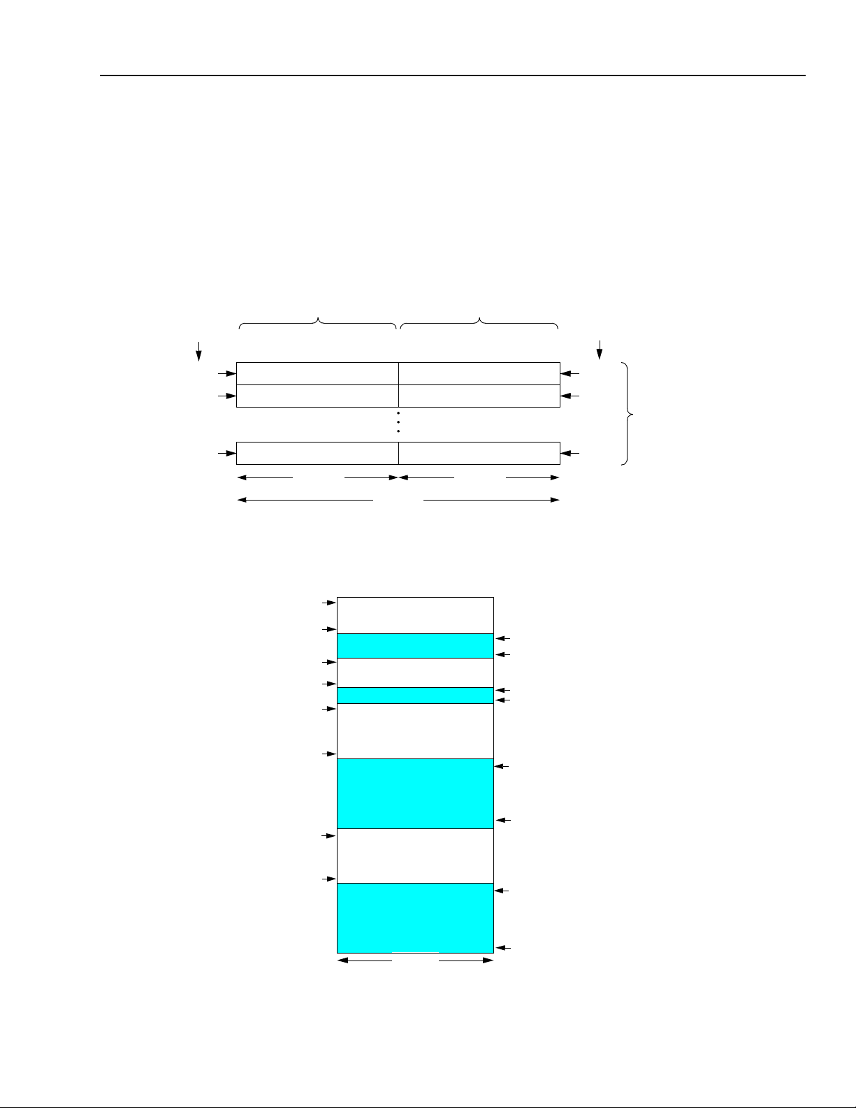
Data Sheet
July 2000 D SP16210 Digital Signal Processor
Hardware Architecture
(continued)
Memory Maps
Figure 5 shows the DSP16210 X-memory space memory map (XMAP). Figure 6 on page 26 shows the DSP16210
Y-memory space memory maps (YMAP0 and YMAP1). Instructions differentiate between the X- and Y-memory
spaces by the addressing unit (i.e., the set of pointers) used for the access and not by the physical memory
accessed. Although the memories are 16-bit word-addressable, data or instruction widths can be either 16 bits or
32 bits and the internal memories can be accessed 32 bits at a time. The internal DPRAM is organized into even
and odd interleaved banks as shown in Figure 4. The core data buses (XDB and YDB) are 32 bits wide, so the core
can access 32-bit DPRAM data that has an aligned (even) address in a single cycle.
11 LSBs
OF
ADDRESS
0x000
0x002
EVEN BANK ODD BANK
16 bits 16 bits
32 bits
11 LSBs
OF
ADDRESS
0x001
0x003
0x7FF0x7FE
DPRAM MODULE
1K x 32 bits
(2 Kwords)
0x00000
.... ...
0x0EFFF
0x1FFC0
0x1FFFD
0x20000
.......
0x21FFF
0x80000
........
0x8FFFF
Figure 4. Interleaved Internal DPRAM
XMAP (16 bits)
MEMORY SEGMENT
DPRAM
60 Kwords
RESERVED
CACHE
62 words
RESERVED
IROM 8 Kwords
(RESET AND SYSTEM TRAP
VECTORS; HDS AND BOOT
CODE)
RESERVED
EROM
(64 Kwords)
RESERVED
†
0x0F000
0x1FFBF
0x1FFFE
0x1FFFF
0x22000
...........
0x7FFFF
0x90000
............
16 bits
† These locations are modularly mapped into the previous segment (EROM). For example, location 0xA0000 maps to location 0x80000.
0xFFFFF
Figure 5. X-Memory Space Memory Map
Lucent Technologies Inc.
DRAFT COPY
25
Page 26
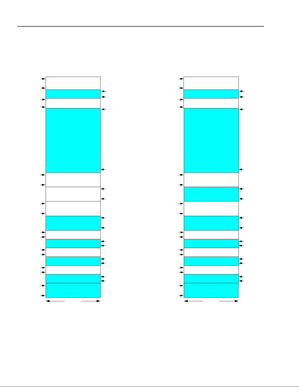
Data Sheet
DSP16210 Digital Signal Processor July 2000
Hardware Architecture
Memory Maps
0x00000
.... ...
0x0EFFF
0x1FFC0
0x1FFFD
0x80000
....
0x8FFFF
0xA0000
....
0xAFFFF
0xC0000
0xC03FF
0xD0000
0xD03FF
0xE0000
0xE003F
0xF0000
....
0xFFFFF
(continued)
YMAP0 (16 bits) YMAP1 (16 bits)
MEMORY SEGMENT
ioc[WEROM] = 0
DPRAM
60 Kwords
RESERVED
CACHE
62 words
RESERVED
ERAMLO
(64 Kwords)
ERAMHI
(64 Kwords)
IO
(64 Kwords)
RESERVED
IORAM0
(1 Kword)
RESERVED
(63 Kwords)
IORAM1
(1 Kword)
RESERVED
(63 Kwords)
(64 words)
RESERVED
(65,504 words)
RESERVED
†
†
†
ESIO
16 bits 16 bits
(continued)
‡
‡
‡
‡
‡
0x0F000
0x1FFBF
0x1FFFE
.........................................
0x7FFFF
0x90000
....
0x9FFFF
0xB0000
....
0xBFFFF
0xC0400
0xCFFFF
0xD0400
0xDFFFF
0xE0040
0xEFFFF
0x00000
.... ...
0x0EFFF
0x1FFC0
0x1FFFD
0x80000
....
0x8FFFF
0xA0000
....
0xAFFFF
0xC0000
0xC03FF
0xD0000
0xD03FF
0xE0000
0xE003F
0xF0000
....
0xFFFFF
MEMORY SEGMENT
ioc[WEROM] = 1
DPRAM
60 Kwords
RESERVED
CACHE
62 words
RESERVED
EROM
(64 Kwords)
RESERVED
(64 Kwords)
RESERVED
IORAM0
(1 Kword)
RESERVED
(63 Kwords)
IORAM1
(1 Kword)
RESERVED
(63 Kwords)
ESIO
(64 words)
RESERVED
(65,504 words)
RESERVED
‡
IO
‡
†
‡
†
‡
†
‡
‡
0x0F000
0x1FFBF
0x1FFFE
...................................... ...
0x7FFFF
0x90000
....
0x9FFFF
0xB0000
....
0xBFFFF
0xC0400
0xCFFFF
0xD0400
0xDFFFF
0xE0040
0xEFFFF
† IORAM0, IORAM1, and ESIO are internal physical memory spaces that are managed by the EMI and are mapped to external memory
addresses.
‡ These locations are modularly mapped into the previous segment. For example, locations 0xD0400—0xD07FF map to locations
0xD0000—0xD03FF and location 0xE0040 maps to location 0xE0000.
Figure 6. Y-Memory Space Memory Maps
The external memory data bus (DB) and the EMI data bus (EDB) are 16 bits wide, and therefore, 32-bit accesses
to external memory and IORAM are broken into two 16-bit accesses.
26
DRAFT COPY
Lucent Technologies Inc.
Page 27

Data Sheet
July 2000 D SP16210 Digital Signal Processor
Hardware Architecture
Memory Maps
The addresses shown in Figures 5 and 6 correspond to
the 20-bit core address buses (XAB for the XMAP and
YAB for YMAP0/YMAP1). For external memory
accesses, these 20-bit addresses are truncated to
16 bits and the external enable pins (EROM, ERAMHI,
ERAMLO, and IO) differentiate the 64K segment being
accessed. For IORAM accesses, these 20-bit
addresses are truncated to 10 bits.
Boot from External ROM
The EXM pin determines from which memory region
(EROM or IROM) the DSP16210 executes code following a device reset. EXM is captured by the rising edge
of RSTB. If the captured value of EXM is one, the
DSP16210 boots from external ROM (EROM—core
address 0x80000). Otherwise, the DSP16210 boots
from internal IROM (core address 0x20000). See
DSP16210 Boot Routines beginning on page 126 for
details on booting from IROM.
(continued)
(continued)
access to the IORAM and ESIO storage. The EMI automatically translates 32-bit XDB/YDB accesses into two
16-bit DB/EDB accesses and vice versa. If an instruction accesses EMI storage from both the X side and Y
side, the EMI performs the X access first followed by
the Y access and the core incurs a conflict wait-state.
The EMI accesses four external memory segments—
ERAMHI, ERAMLO, EROM, and IO.
Two control registers are encoded by the user to define
or
or
mwait
mwait
mwait
ioc
and avail-
update
the operation of the EMI. Bits 14—0 in
(Table58onpage101) and bits 10 and 7—0 in
(Table54onpage99) apply to the EMI. These pro-
grammable features give the designer flexibility in
choosing among various external memories.
Latency for Programming mwait and ioc Registers
There is a two instruction cycle latency between an
instruction that updates either
ability of the new value in the EMI. It is recommended
that two
external memory) follow each
instruction. See the example below:
nop
s (or other instructions that do not access
ioc
ioc
Data Memory Map Selection
The DSP16210 data memory map selection is based
on the value of the WEROM field (bit 4) in the
ter (Table 54 on page 99). If WEROM is set to 0, the
YMAP0 data memory map is selected. If WEROM is
set to 1, the YMAP1 data memory map is selected. If
WEROM is 1, all ERAMLO accesses are redirected to
the EROM segment.
ioc
regis-
External Memory Interface (EMI)
The external memory interface (EMI) manages off-chip
memory and on-chip IORAM memory and ESIO storage, collectively referred to as EMI storage.
The EMI multiplexes the two sets of core buses
(XAB/XDB and YAB/YDB) onto a single set of external
buses—a 16-bit address bus (AB) and 16-bit data bus
(DB). It also multiplexes the two sets of core buses
onto a single set of internal EMI buses—a 10-bit
address bus (EAB) and a 16-bit data bus (EDB)—for
mwait=0x0222/* Modify mwait */
2*nop /* Wait for latency */
a0=*r0 /* OK to perform EMI read */
For write operations the EMI buffers the data (see
Functional Timing beginning on page 29), software
must verify that all pending external write operations
have completed before modifying
mwait
. Software ensures that all memory operations
have completed by ex ecuting an external memory read
operation. After the read operation is completed, it is
ioc
safe to modify
below for an example:
*r1++=a1 /* EMI write. */
a0=*r2 /* Dummy EMI read. */
mwait=0x0222/* Safe to modify mwait. */
2*nop /* Wait for mwait latency. */
Note:
For the EMI to function properly, the application
program
presented above.
mwait
or
must
adhere to the latency restrictions
ioc
or
. See the code segment
Lucent Technologies Inc.
DRAFT COPY
27
Page 28

Data Sheet
DSP16210 Digital Signal Processor July 2000
Hardware Architecture
External Memory Interface (EMI)
Programmable Access Time
For each of the four external memory segments, the number of cycles to assert the enable can be selected in
mwait
(Table 58 on page 101). Within
enable for the IO segment, the Y ATIM[3:0] field specifies the number of cycles to assert the enable for the ERAMLO
and ERAMHI segments, and the XATIM[3:0] field specifies the number of cycles to assert the enable for the EROM
segment. On device reset, all access time values are initialized to 15 (
External memory accesses cause the core to incur wait-states. Table 8 on page 28 defines the duration of an
access and the number of wait-states incurred as a function of the programmed access time (IATIM[3:0],
YATIM[3:0], or XATIM[3:0] abbreviated as A). For example, if YATIM[3:0] = 0xB (decimal 11), then the ERAMLO
and ERAMHI enables are asserted for 11 CLK cycles, any accesses to ERAMLO or ERAMHI require 12 CLK
cycles, and the number of wait-states incurred by the core is 12 for read operations and up to and including 12 for
write operations.
Wait-states for write operations can be transparent to the core if subsequent instructions do not access external
memory.
Table 8. Access Time and Wait-States
Number of CLK Cycles
the Enable Pin Is Asserted
Quantity
Range
IATIM[3:0], YATIM[3:0], or XATIM[3:0]
(abbreviated as ATIM)
(continued)
(continued)
mwait
, the IATIM[3:0] field specifies the number of cycles to assert the
mwait
resets to 0x0FFF).
Duration of
Access
ATIM + 1 ATIM + 1 up to and including ATIM + 1
1—15 2—16 2—16 0—16
Read Write
Wait-States Incurred
READY Pin Enables
For each of the four external memory segments,
disable the READY pin. Setting the RDYEN2 bit enables READY for the IO segment, setting the RDYEN1 bit
enables READY for the ERAMLO and ERAMHI segments, and setting the RDYEN0 bit enables READY for the
EROM segment. On device reset, the RDYEN[2:0] bits are cleared, causing the DSP16210 to ignore the READY
pin by default.
Enable Delays
The leading edge of an enable can be delayed to avoid a situation in which two devices drive the data bus
simultaneously . If the leading edge of an enable is delayed, it is guaranteed to be asserted after the RWN signal is
asserted.
Setting DENB2 of
cycle of CLK. Similarly, setting DENB1 delays the leading edge of the ERAM, ERAMHI, and ERAMLO enables,
and setting DENB0 delays the leading edge of the EROM enable. On device reset, the DENB[2:0] bits are cleared,
causing no delay by default.
Memory Map Selection
The WEROM field (
YMAP1 is selected and all ERAMLO accesses are mapped to EROM. This allows the EROM segment, which is
normally read-only, to be written. For example, a program could download code or coefficients into the EROM segment for later use. If WEROM is set, the DENB1 field (
bits 13 and 7—4) control Y-side accesses to EROM.
ioc
(Table 54 on page 99) delays the leading edge of the IO enable by approximately one half-
ioc
bit 4) selects either YMAP0 or YMAP1 (see Figure 6 on page 26 ). If WEROM is set,
mwait
(Table58onpage101) can be programmed to enable or
ioc
bit 1) and the RDYEN1 and YATIM[3:0] fields (
mwait
28
DRAFT COPY
Lucent Technologies Inc.
Page 29

Data Sheet
July 2000 D SP16210 Digital Signal Processor
Hardware Architecture
External Memory Interface (EMI)
(continued)
(continued)
RWN Advance
The RWNADV field (
ioc
bit 3) controls the amount of delay from the beginning of a write access to the lowering of
the RWN pin. See External Memory Interface under Timing Characteristics and Requirements for details.
CKO Pin Configuration
The CKOSEL[2:0] field (
ioc
bits 7—5) configures the CKO pin as either the internal free-running clock (CLK), the
internal free-running clock held high during low-power standby mode, the output of the CKI input buffer, logic zero,
or logic one. See Table 54 on page 99.
Write Data Drive Delay
The write data delay (WDDLY) field (
ioc
bit 10) controls the amount of time that the EMI delays driving write data
onto the data bus (DB[15:0]). If WDDLY is cleared, the EMI drives the data bus approximately one half-cycle of
CLK after the beginning of the access
of CLK after the beginning of the access
1
. If WDDLY is set, the EMI drives the data bus approximately one full cycle
1
. As a result, setting WDDLY provides an additional delay of one halfcycle for slower external memory. This additional delay is particularly useful if the external memory’s enable is
delayed (the corresponding DENB[2:0] bit is set).
If WDDLY is set, both the turn-on and turn-off delays for the data bus are increased
2
. Because the turn-off delay is
increased, it may be necessary to set the corresponding DENB[2:0] bit for any segments that are read immediately
after writing .
Functional Timing
The following definitions apply throughout:
Low
—an electrical level near ground corresponding to logic zero.
High
—an electrical level near V
Assertion
Deassertion
EMI Storage
—the changing of a signal to its active value.
—the changing of a signal to its inactive value.
—storage that the EMI manages consisting of external memory, IORAM memory, and ESIO memory-
DD
corresponding to logic one.
mapped registers.
EMI Instruction
Non-EMI Instruction
CLK Period
—a DSP16210 instruction that accesses (reads or writes) EMI storage.
—a DSP16210 instruction that does not access EMI storage.
—the time from rising edge to rising edge of the CLK clock; the duration of one single instruction
cycle. All EMI events occur on the rising edge of CLK. It is assumed that the CKO pin is programmed as CLK and
the remainder of this section uses the terms CLK and CKO interchangeably.
1. The beginning of the access occurs when the EMI drops RWN.
2. The data bus active interval is constant regardless of WDDLY.
Lucent Technologies Inc.
DRAFT COPY
29
Page 30

Data Sheet
DSP16210 Digital Signal Processor July 2000
Hardware Architecture
External Memory Interface (EMI)
Functional Timing
(continued)
(continued)
(continued)
All DSP16210 external memory read and write operations consist of two parts:
Active Part
1.
: Lasts for the number of cycles programmed in the
mwait
register (IATIM[3:0], XATIM[3:0], or
YATIM[3:0]). Begins on a rising edge of CLK (CKO). Immediately after this rising edge:
a.The DSP16210 asserts the memory segment enable. If the leading edge of the memory segment enable is
delayed (the corresponding DENB[2:0] bit of
ioc
is set), the DSP16210 asserts the memory segment enable
one-half of a CLK period later.
b.The DSP16210 places the address on the address bus AB[15:0].
c. RWN becomes valid (high for a read, low for a write).
d.For a read operation, the DSP16210 3-states its data bus DB[15:0] drivers. For a write operation, the
DSP16210 delays driving the data bus by an interval determined by the WDDLY field (
ioc
bit 10). If
WDDLY = 0, the delay is approximately one half-cycle of CLK after RWN goes low. If WDDLY = 1, the delay is
approximately one cycle of CLK after RWN goes low.
Finish Part
2.
: Lasts for one cycle. Begins on a rising edge of CLK (CKO). Immediately after this rising edge:
a.The DSP16210 deasserts the memory segment enable.
b.For a read operation, the DSP16210 latches the data from DB[15:0]. For a write operation, the DSP16210 con-
tinues to drive data onto the data bus for an interval determined by the WDDLY field (
ioc
bit 10). If WDDLY = 0,
the DSP16210 drives the bus for approximately one half-cycle of CLK after the beginning of the finish part. If
WDDLY = 1, the DSP16210 drives the bus for appro ximately one cycle of CLK after the beginning of the finish
part.
As a consequence of the finish part of each memory operation, contention problems caused by back-to-back
assertion of different enables (one instruction with dual accesses) are avoided. Following the finish part, the
DSP16210 continues to drive the address bus with the last valid address until the beginning of the next external
read or write operation.
If an instruction
instruction is
where:
If an instruction
incurred by the core during execution of the second
where:
1. Including possible instruction fetch.
2. Wait-states are incurred by the following instruction and not by the current instruction because the EMI internally buffers write data. In other
words, the core does not wait (as it does in the DSP1620) until the write data has been transferred to EMI storage. Instead, the core continues execution while the EMI waits to transfer the data to EMI storage on the next available memory cycle. A subsequent access to EMI storage causes the core to wait until the prior write operation’s data has been transferred to storage.
reads
from EMI storage, the number of wait-states incurred by the core during execution of that
R.R
is computed as:
R = RX + R
X
R
=Number of wait-states incurred from reading external X-memory1.
Y
R
=Number of wait-states incurred from reading external Y-memory, IORAM memory, or ESIO register.
W
= Number of wait-states incurred from writing external Y-memory, IORAM memory, or ESIO register.
Y
writes
to EMI storage and is immediately followed by a second EMI instruction, wait-states are
2
instruction. The number of wait-states is W:
30
DRAFT COPY
Lucent Technologies Inc.
Page 31

Data Sheet
July 2000 D SP16210 Digital Signal Processor
Hardware Architecture
External Memory Interface (EMI)
Functional Timing
Table 9 describes the computation of wait-states for read and write accesses (
(continued)
(continued)
(continued)
X
Y
R
,
R
, and W) for each segment of
EMI storage, including the IORAM memories and ESIO memory-mapped registers.
Table 9. Wait-States
Access Segment Number of Wait-States
X-memory read EROM
Y-memory read ERAMHI or ERAMLO
X
R
Y
R
IO (
IORAM or ESIO (
Y-memory write ERAMHI or ERAMLO
W
‡
IO (
IORAM or ESIO (
†
size
is one for a 16-bit access and two for a 32-bit access.
access or an aligned double-word access.
‡ Write wait-states can be transparent to the core if the EMI write instruction is followed by non-EMI instructions.
misaligned
is one for a misaligned double-word access and zero for a single-word
(
(
(
×
(XATIM[3:0] + 1) +
size
×
(YATIM[3:0] + 1) +
size
×
(IATIM[3:0] + 1) +
size
size
×
(YATIM[3:0] + 1) +
size
×
(IATIM[3:0] + 1) +
size
size+misaligned
×
2+
misaligned
†
misaligned
misaligned
misaligned
)
misaligned
misaligned
)
)
)
)
)
)
Write wait-states can be transparent to the core if the instruction that writes EMI storage is followed by non-EMI
instructions. If write wait-states are transparent, then the core continues execution while the EMI completes the
write operation. For example, the single write external wait-state in the following code segment is transparent and
does not stall the core execution:
*r0++=a0h /* r0 points to IORAM, single-word write, one wait-state */
a0h=a0h+1 /* 1-cycle instruction, no EMI access -- wait-state is transparent */
READY Pin
The READY input pin permits an external device to extend the length of an EMI access cycle. The READY pin can
be used if the number of access cycles programmable in the
mwait
register (Table 58 on page 101) is insufficient,
or if the desired number of access cycles varies from access to access. To use the READY pin for a memory segment access, the access time field in the
grammed to a value of four or greater and the corresponding RDYEN[2:0] field of
time field in
mwait
for the memory segment is less than four or if the RDYEN[2:0] field of
mwait
register (IATIM[3:0], YATIM[3:0], or XATIM[3:0]) must be pro-
mwait
must be set. If the acce ss
mwait
for the memory
segment is cleared, then the DSP16210 ignores the READY pin when accessing that segment. On device reset,
the RDYEN[2:0] fields are cleared, causing the DSP16210 to ignore the READY pin by default. Figure 39 on
page 152 illustrates the operation of the READY pin.
The DSP16210 internally synchronizes the READY pin to the internal clock (CLK). READY must be asserted at
least five cycles (plus a setup time
1
) prior to the end of the external memory operation. The DSP16210 adds the
number of cycles that READY is asserted to the access time.
1. The READY pin setup time is t140 in Table 108 on page 152.
Lucent Technologies Inc.
DRAFT COPY
31
Page 32

Data Sheet
DSP16210 Digital Signal Processor July 2000
Hardware Architecture
(continued)
Enhanced Serial I/O (ESIO) Unit
The ESIO is a programmable, hardware-managed,
double-buffered, full-duplex serial I/O port designed to
support glueless multichannel I/O processing on a
TDM (time-division multiplex) highway. It has a 4-pin
input interface (EIFS, EIBC, EDI, and EIBF) and a 5-pin
output interface (EOFS, EOBC, EDO, EOEB, and
EOBE). See Signal Descriptions beginning on
page 121 for more details. ESIO input and output bit
clocks are passive, i.e., must be provided by an external source. Data is transmitted and received in an
LSB-first manner. The ESIO supports two modes of
operation:
1. Simple mode: Serial I/O that has programmable 8-bit
or 16-bit data lengths. The maximum serial data rate
is 26 Mbits/s.
2. Frame mode: Up to 16 logical channels are multiplexed and demultiplexed on a standard
256-bit/frame TDM highway or on a
64-/128-/192-bit/frame highway
for each channel is individually programmed as 1, 2,
4, or 8 bits corresponding to 8 Kbits/s, 16 Kbits/s,
32 Kbits/s, and 64 Kbits/s for a 2.048 Mbits/s TDM
highway. The maximum supported serial data rate is
8.192 Mbits/s.
The ESIO communicates I/O buffer status to the core
using the input buffer full (EIBF), output buffer empty
(EOBE), input frame error (EIFE), output frame error
(EOFE), and output collision (ECOL) interrupts. The
input buffer full and output buffer empty conditions are
also indicated via the EIBF and EOBE pins. In frame
mode, EIBF and EOBE are based upon the completion
of a programmable number of frames.
The ESIO contains 16 memory-mapped, double-buffered serial-to-parallel input demultiplexer registers
IDMX
0—15
〈
(
be configured to demultiplex a maximum of 16 logical
input channels. A logical input channel is a nonoverlapping sequence of consecutive bits (1, 2, 4, or 8) identified by a starting bit position within the frame.
The ESIO also contains 16 memory-mapped, doublebuffered parallel-to-serial output multiplexer registers
OMX
〈
(
be configured to multiplex a maximum of 16 logical output channels. A logical output channel is a nonoverlap-
1. A single DSP16210 can process up to 128 bits/frame (sixteen
8-bit channels).
0—15
〉
). These 16-bit read-only registers can
〉
). These 16-bit write-only registers can
1
. The sample length
ping sequence of consecutive bits (1, 2, 4, or 8)
identified by a starting bit position within the frame.
The ESIO’s serial data output (EDO) supports multimaster operation and can be configured as open-drain
or 3-state.
Input Section
The control registers in the ESIO input section are the
input control register (
ICSB
0—7
isters (
ICSL
ters (
register (
All the ESIO input section registers are 16 bits and are
memory-mapped as illustrated in Table 10.
Table 10. ESIO Memory Map (Input Section)
Memory
Address
0xE0000
0xE0001
0xE0002
0xE0003
0xE0004
0xE0005
0xE0006
0xE0007
0xE0008
0xE0009
0xE000A
0xE000B
0xE000C
0xE000D
0xE000E
0xE000F
† This column indicates whether the register is readable (R) and/or
writable (W).
The input control register (
controls the configuration of the input section, including
the selection of simple mode vs. frame mode.
(Table 50 on page 96) specifies the number of active
logical channels (one for simple mode and 1 through
16 for frame mode).
ICSL
and
in frame mode. They specify the starting bit position
and the sample length (1, 2, 4, or 8 bits) of each logical
channel.
〈
0—1
〈
ICVV
). The data registers are
Register R/W
IDMX0
IDMX1
IDMX2
IDMX3
IDMX4
IDMX5
IDMX6
IDMX7
IDMX8
IDMX9
IDMX10
IDMX11
IDMX12
IDMX13
IDMX14
IDMX15
0—1
〈
ICR)
, input channel start bit reg-
〉)
, input channel start length regis-
〉)
, and input channel valid vector
0—15
IDMX
〈
†
Memory
Address
R 0xE0010
R 0xE0011
R 0xE0012
R 0xE0013
R 0xE0014
R 0xE0015
R 0xE0016
R 0xE0017
R 0xE0018
R 0xE0019
R 0xE001A
R 0xE001B
R 0xE001C
R 0xE001D
R 0xE001E
R 0xE001F
ICR
) (Table 47 on page 95)
ICSB
0—7
〈
〉
(Table 48 on page 96)
〉
(Table 49 on page 96) are used only
Register R/W
ICSB0
ICSB1
ICSB2
ICSB3
ICSB4
ICSB5
ICSB6
ICSB7
ICSL0
ICSL1
ICR
ICVV
R
E
S
E
R
V
ICVV
R/W
R/W
R/W
R/W
R/W
R/W
R/W
R/W
R/W
R/W
R/W
R/W
E
〉
.
D
†
32
DRAFT COPY
Lucent Technologies Inc.
Page 33

Data Sheet
IBC
IFS
EDI
B
0
B
1
DATA
INTERNAL
BIT COUNTER
CLEARED
LATCHED
DATA
LATCHED
July 2000 D SP16210 Digital Signal Processor
Hardware Architecture
Enhanced Serial I/O Unit (ESIO)
(continued)
(continued)
ESIO interrupts are summarized in Table 14 on
page 41.
Input Control Signal Conditioning.
Figure 7, ILEV (bit 3) of the
ICR
As illustrated in
register (Table 47 on
page 95) selects the polarity of the input bit clock,
EIBC. The modified clock is the input bit clock for the
input section (IBC). The input sync level, ISLEV (bit 5)
ICR
of the
register, selects whether or not the input
frame sync, EIFS, is inverted. If input sync delay
(ISDLY) (bit 6) of the
ICR
register is zero, this modified
signal is the frame sync for the input section (IFS). If
ISDLY is one, the modified signal is first retimed by the
EIBC clock before becoming the frame sync for the
input section (IFS). Figure 8 illustrates the timing of
IFS when ISDLY is one.
0
M
U
IFS
EIFS
EIBC
DQ
ISLEV
ILEV
X
1
ISDLY
IBC
FRAME SYNC
AND
CLOCK
FOR
ESIO
INPUT
SECTION
Figure 7. Input Control Signal Conditioning
EIBC
EIFS
packet or frame (from EDI) is captured by the falling
edge of IBC. This edge also initializes the internal bit
counter to zero, and every subsequent rising edge of
IBC increments the bit counter. In frame mode, this bit
counter is used by the input control hardware to define
logical channel start points and to detect input frame
errors. See Figure 9.
Figure 9. Input Functional Timing
Simple Input Mode Processing.
The ESIO input
block operates in simple input mode when IMODE
(bit 8) of the
programmer must set the
ICR
register is set to 1. In this mode, the
ICVV
register to 0x 000 1. Th e
ESIO disables the input frame error interrupt (EIFE).
In simple mode, the ESIO supports double-buffered
8-bit and 16-bit LSB-first serial operation. Eight-bit
serial operation is selected by setting ISIZE (bit 7) of
ICR
the
i.e., the 8-bit data is aligned with bits [7:0] of
register. This right justifies 8-bit input packets,
IDMX0
.
See Figure 10 on page 34 for a diagram of the input
demultiplexer structure. Serial input data from EDI is
captured into a serial-to-parallel register by the falling
edge of IBC (illustrated as IBCQ0 in Figure 10). After
all programmed bits (8 or 16) have been captured, the
data is transferred to the parallel data register
for future core processing (for example,
IDMX0
a0h = *r0
,
where r0 points to location 0xE0000).
IFS
Figure 8. Frame Sync Timing with ILEV = ISLEV = 0
and ISDLY = 1
The rising edge of IFS (captured by the next rising
edge of IBC) indicates that the first bit of the serial input
Lucent Technologies Inc.
DRAFT COPY
The ESIO asserts the input buffer full (EIBF) output pin
and the EIBF interrupt after the falling edge of the final
IBC capture clock. The EIBF interrupt and pin are
cleared when the DSP reads the
IDMX0
memorymapped register. EIBF is also cleared on device reset
or if the DSP program resets the input section (writes
ICR
with the IRESET field (bit 4) set). The simple mode
input timing diagram (for ILEV = 0, ISLEV = 0,
ISIZE = 0, and ISDLY = 0) is illustrated in Figure 52 on
page 166.
33
Page 34

Data Sheet
DSP16210 Digital Signal Processor July 2000
Hardware Architecture
(continued)
Enhanced Serial I/O Unit (ESIO)
EDI
0
M
U
X
1
0
ISIZE
0
M
U
X
1
0
ISIZE
SERIAL-TO-PARALLEL
IBCQ0 IBCQ0
IDLD0
SERIAL-TO-PARALLEL
IBCQ1 IBCQ1
8-bit
REGISTER
8 8
8-bit
REGISTER
8 8
(continued)
1
0
ISIZE
IDMX0
1
0
ISIZE
M
U
X
16
M
U
X
SERIAL-TO-PARALLEL
SERIAL-TO-PARALLEL
8-bit
REGISTER
8-bit
REGISTER
USED
IN
SIMPLE
AND
FRAME
MODES
IDLD1
0
M
U
X
1
0
ISIZE
SERIAL-TO-PARALLEL
IBCQ15 IBCQ15
IDLD15
8-bit
REGISTER
8 8
IDMX1
16
1
0
ISIZE
IDMX15
16
USED
IN
FRAME
MODE
ONLY
M
U
X
SERIAL-TO-PARALLEL
8-bit
REGISTER
EAB[3:0]
16 16 16
MUX
0115
16
34
TO EDB[15:0]
Figure 1 0. Input Demultiplexer (IDMX) and Register File Structure
DRAFT COPY
Lucent Technologies Inc.
Page 35

Data Sheet
IBC
EDI
B
63
B
62
B
64
B
65
IBCQ3
July 2000 D SP16210 Digital Signal Processor
Hardware Architecture
Enhanced Serial I/O Unit (ESIO)
Frame Input Mode Processing.
frame input mode (IMODE) when (bit 8) of the
(continued)
(continued)
The ESIO operates in
ICR
register is cleared. (IMODE is cleared on reset.) The ESIO
demultiplexes multiple channels from a serial stream
consisting of a frame of 64, 128, 192, or 256 bits. The
input frame size (IFRMSZ) is specified by (bits [11:10])
ICR
of the
register. The start of a new frame is signaled
by the rising edge of the input frame sync (IFS). The
ESIO ignores input until it has detected the beginning
of a valid frame. Serial data is captured by the falling
edge of the input bit clock (IBC) (see Figure 9 on
page 33).
See Figure 10 on page 34 for a diagram of the
IDMX
structure. The input section contains 16 double-buffered 16-bit serial-to-parallel input demultiplexers with
provision for either 8-bit (ISIZE = 1) or 16-bit (ISIZE =
0) right-justified data. Each logical channel has a dedicated 16-bit shift register that receives demultiplexed
serial data and has a dedicated 16-bit parallel read reg-
IDMX
0—15
ister (
〈
〉
). Each shift register is clocked individually by IBCQ[15:0], a qualified IBC bit clock that
starts when the internal bit counter matches the input
logical channel start bit specified by the corresponding
ICSB
0—7
〈
〉
register (see Table 11).
ple length for the corresponding logical channel. The
0—1
ICSL
〈
〉
sample length is specified by one of the
registers (see Table 49 on page 96).
Figure 11 is a timing diagram that depicts the clock
IBCQ3 assuming that the sample length is 2 bits
ICSL0
(
(
[7:6] = 01) and the start bit is 63
ICSB1
[15:8] = 0x3F). In this example, bits B
63
and B64
are clocked into the shift register for logical channel 3.
When 16 serial input bits have been captured for a
given channel
n
, the ESIO asserts IDLDn (see
Figure 10 on page 34), transferring the shift register
IDMX
contents to the channel’s parallel read register,
n
This transfer occurs every 2, 4, 8, or 16 frames
depending on the sample length programmed for chan-
0—1
ICSL
〈
nel
n
via
〉
. This serial-to-parallel transfer
permits a 16-bit word of channel data to be captured (at
the IBC rate) while the previous word is read by the
core.
.
Table 11. Input Channel Start Bit Registers
15—8 7—0
ICSB0
ICSB1
ICSB2
ICSB3
ICSB4
ICSB5
ICSB6
ICSB7
Channel 1 Channel 0
Channel 3 Channel 2
Channel 5 Channel 4
Channel 7 Channel 6
Channel 9 Channel 8
Channel 11 Channel 10
Channel 13 Channel 12
Channel 15 Channel 14
Field Value Description
Channel 0
to
Channel
0x00
0xFF
Start bit position for corresponding
to
logical input channel.
Ranges from 0 to 255.
15
The clock IBCQ[15:0] is asserted in each frame for the
number of cycles that matches the programmed sam-
Figure 11. Serial Input Clocking Example
The ESIO is programmed to generate the input buffer
full (EIBF) interrupt and assert the EIBF output pin at
the completion of every 2, 4, 8, or 16 frames depending
on the IFIR field of the
ICR
register (Table 47 on
page 95). EIBF is cleared if the DSP program reads
any of the
section (writes
〈
ICR
〉
registers or if it resets the input
with the IRESET field (bit 4) set).
IDMX
0—15
EIBF is first asserted when the programmed number of
input frames have been received following initialization
of the ESIO input section. The programmer initializes
the input section by simultaneously resetting it and
enabling it, i.e., by writing
ICR
with the IRESET field set
and the ICA field (bit 2) set. The IRESET field clears
itself automatically every cycle of the internal clock
(CLK). Therefore, when
ICR
is read, the value of the
IRESET field is always clear.
Lucent Technologies Inc.
DRAFT COPY
35
Page 36

Data Sheet
DSP16210 Digital Signal Processor July 2000
ICVV
Hardware Architecture
Enhanced Serial I/O Unit (ESIO)
Prior to initializing the input section as described
above, the programmer must configure
ICSB
0—7
〈
〉
, and
tializes the input section must also configure the input
section appropriately (IMODE, IFRMSZ, etc.). Before
changing any input channel attributes (e.g.,
IMODE), the programmer must first reset the input section. Specifically, the programmer must write
the IRESET field (bit 4) set and the ICA field (bit 2)
clear, change the attributes, and then enable the input
section by writing
In an environment with several different logical channel
sampling lengths, the EIBF generation rate should be
set to the highest serial-to-parallel transfer rate (see
Table 49 on page 96). Each channel is serviced at it s
programmed rate when a full word of input data is provided. For example, in a system with logical channels
of sample length 1, 2, and 8 bits, the highest serial-toparallel transfer rate is every two frames and IFIR
should be programmed to 0 (one EIBF every two
frames). The channels with an 8-bit sample length
should be serviced every EIBF interrupt, the channels
with a 2-bit sample length should be serviced every
four EIBF interrupts, and the channels with a 1-bit sample length should be serviced ev ery eight EIBF interrupts.
The ITMODE field (bit 9) of
to-parallel transfer rate specified by
ITMODE is set to 1, data is transferred from each input
shift register to all sixteen
simultaneously at the programmed IFIR frequency . The
ESIO asserts EIBF for each transfer. It is not necessary
to reset the ESIO prior to changing the ITMODE bit.
Note:
In ITMODE, input data is not necessarily rightjustified in
stream is continuously shifted into the MSB (8-bit
or 16-bit) location of each shift register. The contents of the shift registers are transferred to the
IDMX
quency.
The logical channels are enabled by programming the
ICVV
16-bit
sponds to a logical channel, e.g., bit 5 of
sponds to logical channel 5. When a bit in
the ESIO demultiplexes the input data stream for the
corresponding channel. The bits in
packed, i.e., channels must be allocated from 0 to 15
with no holes between valid channels. For example, if
IDMX
0—15
〈
register. Each bit in this register corre-
0—1
ICSL
〈
ICR
with the ICA field (bit 2) set.
0—15
〈
〉
registers at the alternate IFIR fre-
(continued)
(continued)
ICVV
〉
. The write of
ICR
can override the serial-
ICSL
0—1
〈
IDMX
0—15
〈
〉
. The LSB of the data
〉
ICVV
registers
ICVV
ICVV
must be
,
ICR
ICVV
ICR
that ini-
,
with
〉
. When
corre-
is set,
contains 0x00FF, then logical channels 0—7 are
enabled and demultiplexed. A value of 0x08FF for
is invalid because the channels are not packed.
Logical channels must be assigned in increasing input
channel start bit order and must not overlap. For example, if channel 4 has a start bit of 48 and a sample
length of 4 bits (
then channel 5 must have a start bit value greater than
or equal to 52 (48 + 4).
The ESIO reports an input frame error (EIFE) when it is
processing a valid frame and an input frame sync is
detected before the number of bits in the programmed
frame length (IFRMSZ in
an EIFE interrupt occurs, the DSP program should
reset the input section by writing
bit set.
Output Section
The control registers in the ESIO output section are the
output control register (
bit registers (
length registers (
valid vector register (
OMX
0—15
〈
16 bits and are memory mapped as illustrated in
Table 12.
Table 12. ESIO Memory Map (Output Section)
Memory
Address
0xE0020
0xE0021
0xE0022
0xE0023
0xE0024
0xE0025
0xE0026
0xE0027
0xE0028
0xE0029
0xE002A
0xE002B
0xE002C
0xE002D
0xE002E
0xE002F
† This column indicates whether the register is readable (R) and/or
writable (W).
ICSB2
[7:0] = 0x30;
ICR
) have been sampled. If
OCR
), the output channel start
OCSB
〉
. All the ESIO output section registers are
Register R/W
OMX0
OMX1
OMX2
OMX3
OMX4
OMX5
OMX6
OMX7
OMX8
OMX9
OMX10
OMX11
OMX12
OMX13
OMX14
OMX15
0—7
〈
OCSL
OCVV
〉
), the output channel sample
0—1
〈
〉
). The data registers are
†
Memory
Address
W 0xE0030
W 0xE0031
W 0xE0032
W 0xE0033
W 0xE0034
W 0xE0035
W 0xE0036
W 0xE0037
W 0xE0038
W 0xE0039
W 0xE003A
W 0xE003B
W 0xE003C
W 0xE003D
W 0xE003E
W 0xE003F
ICSL0
[9:8] = 10),
ICR
with the IRESET
), and the output channel
Register R/W
OCSB0
OCSB1
OCSB2
OCSB3
OCSB4
OCSB5
OCSB6
OCSB7
OCSL0
OCSL1
OCR
OCVV
R
ICVV
R/W
R/W
R/W
R/W
R/W
R/W
R/W
R/W
R/W
R/W
R/W
R/W
E
S
E
R
V
E
D
†
36
DRAFT COPY
Lucent Technologies Inc.
Page 37

Data Sheet
OBC
OFS
EDO
B
0
B
1
INTERNAL
BIT COUNTER
CLEARED
EOEB
EOBE
July 2000 D SP16210 Digital Signal Processor
Hardware Architecture
Enhanced Serial I/O Unit (ESIO)
OCR
(Table 59 on page 102) controls the configuration
(continued)
(continued)
of the output section, including the selection of simple
mode vs. frame mode.
OCVV
(Table 62 on page 103)
specifies the number of active logical channels (one for
simple mode and 1 through 16 for frame mode).
OCSB
0—7
〈
〉
(Table 60 on page 103) and
OCSL
0—1
〈
(Table 61 on page 103) are used only in frame mode.
They specify the starting bit position and the sample
length (1, 2, 4, or 8 bits) of each logical channel.
As illustrated in Figure 12, OLEV (bit 3) of the
OCR
register selects the polarity of the output bit clock,
EOBC. This modified clock is the output bit clock for
the output section (OBC). OSLEV (bit 8) of the
OCR
register selects whether or not the output frame sync,
EOFS, is inverted. This modified signal is the frame
sync for the output section (OFS).
EOFS
EOBC
OSLEV
(OCR[8])
OLEV
(OCR[3])
OFS
OBC
FRAME SYNC
AND
CLOCK
FOR
ESIO
OUTPUT
SECTION
Figure 12. Output Control Signal Conditioning
As illustrated in Figure 13, the ESIO drives serial data
onto the ESIO data out (EDO) pin the rising edge of the
output bit clock (OBC). The rising edge of output frame
sync (OFS) indicates that the first bit of the serial output packet or frame is driven onto EDO on the next rising edge of OBC. This edge (as captured by OBC) also
initializes the internal bit counter to zero, and every
subsequent rising edge of OBC increments the bit
counter. In frame mode, this bit counter is used by the
output control hardware to define logical chann el sta rt
points and to detect output frame errors.
The ESIO asserts the EOBE output pin and the EOBE
interrupt on the falling edge of OBC following detection
of OFS as shown in Figure 13. EOBE is cleared when
OMX
0—15〉
the DSP program writes any of the
〈
ory-mapped registers. EOBE is also cleared on device
reset or if the DSP program resets the output section
by writing the
(bit 4) set.
〉
OCR
register with the ORESET field
Figure 13. Output Functional Timing
The ESIO drives EDO only during its scheduled
timeslot as illustrated in Figure 13. Otherwise EDO is in
the high-impedance state. The other necessary conditions for the DSP16210 to drive EDO are:
■
The EOEB negative-assertion input pin must be
asserted (low).
■
The EDOEO bit in the
OCR
register (bit 6) must be
set.
If EOEB is high or if the EDOEO bit is cleared, then
EDO is in the high-impedance state regardless of the
state of ESIO output section. The EDOEO bit is cleared
on reset causing the EDO pin to be in the high-impedance state by default.
The EDOMD bit in
OCR
(bit 5) configures the EDO out-
put pin driver as either 3-state or open-drain.
mem-
Lucent Technologies Inc.
DRAFT COPY
37
Page 38

Data Sheet
DSP16210 Digital Signal Processor July 2000
Hardware Architecture
(continued)
Enhanced Serial I/O Unit (ESIO)
USED
IN
SIMPLE
AND
FRAME
MODES
ODLD0
OBCQ0
OBCQ1
(continued)
FROM
EDB[15:0]
16
OMX0
16
16-bit PARALLEL-TO-SERIAL REGISTER
16
OMX1
16
16-bit PARALLEL-TO-SERIAL REGISTERODLD1
EDO0
EDO1
EDO15
0115
MUX
OCIX[15:0]
EDO
USED
IN
FRAME
MODE
ONLY
16
OMX15
16
16-bit PARALLEL-TO-SERIAL REGISTERODLD15
OBCQ15
Figure 14. Output Multiplexer (OMX) and Register File Structure
38
DRAFT COPY
Lucent Technologies Inc.
Page 39

Data Sheet
July 2000 D SP16210 Digital Signal Processor
Hardware Architecture
Enhanced Serial I/O Unit (ESIO)
Simple Output Mode Processing.
block operates in simple mode when OMODE (bit 10)
OCR
of the
grammer must set the
ESIO disables the output frame error (EOFE) and output collision (ECOL) interrupts.
In simple mode, the ESIO supports double-buffered
8-bit and 16-bit LSB-first serial operation. Eight-bit
serial operation is selected by setting OSIZE (bit 9) of
OCR
the
See Figure 14 on page 38 for a diagram of the output
multiplex er str uctur e. The prog ram writes 8-bit or 16- bit
data into the
justified in
clock after frame sync (OFS) detection, the data is
transferred from
register (ODLD0 in Figure 14 is asserted). During this
same OBC clock (illustrated as OBCQ0 in Figure 14),
the LSB of the data (B
each subsequent rising edge of OBC, the remaining
bits are applied to EDO. The simple mode output timing
diagram (for OLEV = 0, OSLEV = 0, and OSIZE = 0) is
illustrated in Figure 53 on page 167.
register is set to 1. In this mode, the pro-
OCVV
register.
OMX0
register. (8-bit data must be right-
OMX0
). On the rising edge of the first OBC
OMX0
to the 16-bit parallel-to-serial
0
) is applied to the EDO pin. On
(continued)
(continued)
The ESIO output
register to 0x0001. The
See Figure 14 on page 38 for a diagram of the output
multiplexed into EDO. The output section contains
16 double-buffered 16-bit parallel-to-serial output multiplexers. Each logical channel has a dedicated 16-bit
OMX
0—15
〈
parallel write register (
cated 16-bit shift register that transmits serial data for
that channel. Each shift register is clocked individually
by OBCQ[15:0], a qualified OBC bit clock that starts
when the in ternal bit counter m atches t he outp ut logic al
channel start bit specified by the corresponding
OCSB
Table 13. Output Channel Start Bit Registers
0—7
〈
〉
register (see Table 13).
15—8 7—0
OCSB0
OCSB1
OCSB2
OCSB3
OCSB4
OCSB5
OCSB6
OCSB7
Field Value Description
Channel 0
to
Channel 15
Channel 1 Channel 0
Channel 3 Channel 2
Channel 5 Channel 4
Channel 7 Channel 6
Channel 9 Channel 8
Channel 11 Channel 10
Channel 13 Channel 12
Channel 15 Channel 14
0x00
0xFF
Start bit position for correspond-
to
ing logical output channel.
Ranges from 0 to 255.
〉
) and has a dedi-
Frame Output Mode Processing.
in frame output mode when OMODE (bit 10) of the
OCR
register is cleared. (OMODE is cleared on reset.)
The ESIO multiplexes up to 16 channels of data onto a
serial stream consisting of a frame of 64, 128, 192, or
256 bits. The frame size is specified by OFRMSZ
(bits [13:12]) of the
frame is signaled by the rising edge of the output frame
sync (OFS). Serial data is captured by the falling edge
of the output bit clock (OBC) (see Figure 13 on
page 37).
OCR
register. The start of a new
The ESIO operates
OMX
0—15
〈
registers that are written if the core writes to the corresponding memory location (see Table 12 on page 36).
The ESIO asserts ODLD
Figure 14 on page 38) to load the channel’s parallel-to-
serial register with the contents of the
All 16 parallel-to-serial registers are loaded simultaneously when the first frame sync (OFS) is asserted
following initialization of the output section. (See the
following discussion for a description of output section
initialization.) The parallel-to-serial register for
channel
every 2, 4, 8, or 16 frames depending on the sample
length programmed for channel
Table 61 on page 103). This transfer permits the core
to write a new 16-bit word of channel data into
while the old word is shifted out serially.
〉
are 16-bit write-only memory-mapped
n
for logical channel n (see
OMX
n
register.
n
is subsequently loaded (ODLDn asserted)
n
via
OCSL
0—1
〈
〉
OMX
(see
n
Lucent Technologies Inc.
DRAFT COPY
39
Page 40

Data Sheet
DSP16210 Digital Signal Processor July 2000
Hardware Architecture
Enhanced Serial I/O Unit (ESIO)
(continued)
(continued)
The clock OBCQ[15:0] is asserted in each frame for the
number of cycles that matches the programmed sample length for the corresponding logical channel. The
sample length is specified by one of the
OCSL
0—1
〈
〉
registers (see Table 61 on page 103).
Figure 15 is a timing diagram of the clock OBCQ3, the
bit clock for logical channel 3, assuming that the sample length is 2 bits (
OCSB1
is 63 (
OCSL0
[7:6] = 01) and the start bit
[15:8] = 0x3F). In Figure 15, D
0
is the
LSB and the initial output of the channel 3 parallel-toserial register (EDO3). The ESIO asserts the OCIX3
signal during the time slot for logical channel 3,
enabling EDO3 onto the EDO pin (see Figure 14 on
page 38). OBCQ3 is asserted for two cycles, shifting
the parallel-to-serial register contents by two bit positions, leaving D
OBC
OBCQ3
EDO3
OCIX3
EDO
2
on EDO3 for the next frame.
0
D
62
B
B63 = D0 B64 = D
1
D
1
2
D
65
B
Figure 15. Serial Output Clocking Example
The ESIO asserts the EOBE output pin and the EOBE
interrupt on the falling edge of OBC after the detection
of the first OFS following output section initialization.
(See Figure 13 on page 37 for an illustration of EOBE
timing and the discussion below for a description of
output section initialization.) EOBE is cleared when the
OMX
0—15〉
DSP program writes an y of the
〈
memorymapped registers. EOBE is also cleared on device
reset or if the DSP program resets the output section
by writing the
OCR
register with the ORESET field
(bit 4) set. The ESIO reasserts EOBE at the completion
of every 2, 4, 8, or 16 frames depending on the OFIR
field (bits [1:0]) of the
OCR
register (Table 59 on
page 102).
The programmer initializes the output section by simultaneously resetting it and enabling it, i.e., by writing
OCR
with the ORESET field set and the OCA field
(bit 2) set. The ORESET field clears itself automatically
every cycle of the internal clock (CLK). Therefore,
OCR
when
is read, the value of the ORESET field is
clear.
Prior to initializing the output section as described
above, the programmer must configure
OCSB
0—7
〈
〉
, and
OCSL
0—1
〈
〉
. The write of
OCVV
,
OCR
that
initializes the output section must also configure the
output section appropriately (OMODE, OFRMSZ, etc.).
Before changing any output channel attributes (e.g.,
OCVV
, OMODE), the programmer must first reset the
output section. Specifically, the programmer must write
OCR
with the ORESET field (bit 4) set and the OCA
field (bit 2) clear, change the attributes, and then
enable the out put sec tio n by w riting
OCR
with the OCA
field (bit 2) set.
In an environment with several different logical channel
sampling lengths, the EOBE generation rate should be
set to the highest parallel-to-serial transfer rate (see
Table 61 on page 103). Each channel is serviced at its
programmed rate when a full word of output data has
been transmitted. For example, in a system with logical
channels of sample length 1, 2, and 8 bits, the highest
parallel-to-serial transfer rate is every 2 frames and
OFIR should be programmed to 0 (one EOBE every 2
frames). The channels with an 8-bit sample length
should be serviced every EOBE interrupt, the channels
with a 2-bit sample length should be serviced every
four EOBE interrupts, and the channels with a 1-bit
sample length should be serviced every eight EOBE
interrupts.
The OTMODE field (bit 11) of
parallel-to-serial transfer rate specified by
OCR
can override the
OCSL
0—1
〈
〉
When OTMODE is set to 1, data is transferred from
OMX
0—15
each
〈
〉
register to all 16 output shift registers simultaneously at the programmed OFIR frequency.
The logical channels are enabled by programming the
OCVV
16-bit
sponds to a logical channel, e.g., bit 5 of
sponds to logical channel 5. When a bit in
register. Each bit in this register corre-
OCVV
corre-
OCVV
is set,
the ESIO multiplexes the output serial stream with data
from the corresponding channel. The bits in
OCVV
must be packed, i.e., channels must be allocated from
0 to 15 with no holes between valid channels. For
example, if
OCVV
contains 0x00FF, then logical channels 0—7 are enabled and multiplexed. A value of
0x08FF for
OCVV
is invalid because the channels are
not packed.
.
40
DRAFT COPY
Lucent Technologies Inc.
Page 41

Data Sheet
July 2000 D SP16210 Digital Signal Processor
Hardware Architecture
(continued)
gram should reset the output section by writing
with the ORESET bit set.
Enhanced Serial I/O Unit (ESIO)
(continued)
When driving output data in frame mode with EDO programmed as an open-drain device (EDOMD = 1 and
Logical channels must be assigned in increasing output
channel start bit order and must not overlap. For example, if channel 4 has a start bit of 48 and a sample
length of 4 bits (
OCSB2
[7:0] = 0x30;
OCSL0
[9:8] =
10), then channel 5 must have a start bit value greater
than or equal to 52 (48 + 4).
The ESIO reports an output frame error (EOFE) when
it is processing a valid frame and an output frame sync
is detected before the number of bits in the programmed frame length (OFRMSZ in
OCR
) have been
transmitted. If an EOFE interrupt occurs, the DSP pro-
EDOEO = 1), the ESIO samples the EDO pin every
EOBC clock cycle. If the sampled value is not the
intended output value, the ESIO has collided with
another serial bus agent. When a bus collision is
detected, the ESIO asserts the output collision interrupt (ECOL) . The DSP pr ogr am clear s ECOL b y writin g
OCR
with either the ORESET field (bit 4) or the CRE-
SET field (bit 7) set.
Table 14 summarizes the ESIO interrupts. See Table 7
on page 23 for information on request clearing latency
for these interrupts.
Table 14. ESIO Interrupts
Interrupt Name Description Cleared By
EIBF Input
Buffer
Full
Simple Mode
(IMODE = 1)
Frame Mode
(IMODE = 0)
Asserted if a programmed number of input
bits (8 or 16 depending on ISIZE (
ICR
[7]))
have been captured following assertion of
the input frame sync.
Asserted after N input frames (N = 2, 4, 8,
or 16, depending on IFIR[1:0] (
ICR
[1:0]))
have been received following input section
initialization
†
. If ICA (
ICR
[2]) remains set,
Any of the following:
■
Device reset.
■
DSP program reads any of
0—15
IDMX
〈〈〈〈
■
The DSP program sets the
IRESET field (
〉〉〉〉
.
ICR
EIBF is reasserted after every subsequent
N
frames have been received.
‡
EIFE
Input
Frame
Error
Frame Mode
(IMODE = 0)
Asserted if the input section is processing a
valid frame and an input frame sync is
detected before the number of bits specified by IFRMSZ[1:0] (
ICR
[11:10]) have
The DSP program sets the
IRESET field (
ICR
[4]).
been sampled.
EOBE Output
Buffer
Empty
‡
EOFE
Output
Frame
Error
Simple Mode
(OMODE = 1)
Frame Mode
(OMODE = 0)
Frame Mode
(OMODE = 0)
Asserted after the first bit (LSB) has been
output.
Asserted after the first bit (LSB) of the first
frame has been output following output
section initialization
§
. If OCA (
OCR
[2])
remains set, EOBE is reasserted at the
completion of every 2, 4, 8, or 16 frames
depending on OFIR[1:0] (
OCR
[1:0]).
Asserted if the output section is processing
a valid frame and an output frame sync is
detected before the number of bits in the
Any of the following:
■
Device reset.
■
DSP program writes
0—15
OMX
any of
■
The DSP program sets the
ORESET field (
〈〈〈〈
OCR
The DSP program sets the IRESET field.
programmed frame length OFRMSZ[1:0]
OCR
(
[13:12]) have been transmitted.
‡
ECOL
Output
Collision
Frame Mode
(OMODE = 0)
Asserted if EDO is an open-drain output
(EDOMD (
OCR
(
OCR
[5]) = 1 and EDOEO
[6]) = 1) and the sampled EDO pin
The DSP program sets the
ORESET field (
CRESET field (
OCR
OCR
value is not the intended output value.
† The DSP program initializes the input section by setting IRESET (
‡ This interrupt is disabled in simple mode.
§ The DSP program initializes the output section by setting ORESET (
ICR
[4]) and ICA (
OCR
[4]) and OCA (
ICR
[2]).
OCR
[2]).
OCR
[4]).
〉〉〉〉
.
[4]).
[4]) or the
[7]).
Lucent Technologies Inc.
DRAFT COPY
41
Page 42

Data Sheet
DSP16210 Digital Signal Processor July 2000
Hardware Architecture
(continued)
Modular I/O Units (MIOUs)
The DSP16210 contains two identical modular I/O
units: MIOU0 (provides DMA for the PHIF16) and
MIOU1 (provides DMA for the SSIO).
An MIOU provides programmable DMA capability.
Figure 16 shows the MIOUs, their connections to the
IORAMs, the attached I/O peripherals, and the IDB.
Each MIOU interfaces its attached peripheral to a single 1 Kword bank of IORAM storage that resides in the
DSP16000 core’s Y-memory space. Input and output
buffers for each peripheral are allocated in each
IORAM.
DSP16000 CORE
XDB XAB YDB YAB IDB
IDB
EDB
EAB
16 10 1610
3232 20 3220
EMI
16 10
IORAM
IORAM storage consists of two 1 Kword banks of memory , IORAM0 and IORAM1. Each IORAM bank has two
16-bit data and two 10-bit address ports. An IORAM
bank can be shared by the core and an MIOU to implement a DMA-based I/O system. IORAM supports concurrent core execution and MIOU I/O processing.
Portions of IORAM not dedicated to I/O processing can
be used as general-purpose data storage. However, a
high collision rate between core and MIOU accesses to
IORAM impacts core and I/O performance.
The IORAMs reside in the core’s Y-memory space (see
Figure 6 on page 26). The EMI interfaces the core to
the IORAMs by translating between YAB/YDB
accesses and EAB/EDB accesses. This translation is
functionally transparent to the programmer. The core
can access the IORAM as single words or as double
words and the EMI automatically performs the required
multiplexing and sequencing. Core accesses to IORAM
cause the core to incur wait-states (see External Mem-
ory Interface (EMI) beginning on page 27). If the core
and an MIOU simultaneously access the same IORAM,
the MIOU access occurs first followed by the core
access and the core incurs a conflict wait-state.
MIOU Registers
data address dataaddress
IORAM0
1K
data address
MIOU0
mcmd0
miwp0
morp0
PHIF16
Figure 16. Modular I/O Units
Table 15. Instructions for Programming MIOU Registers
Instruction Syntax Substitution Example
RAB = IM20 RAB
RB = aTE〈h, l
aTE〈h, l〉=RB
〉
RB
IORAM1
1K
1016 1610
MIOU1
mcmd1
miwp1
morp1
SSIO
dataaddress
mcmd〈0, 1
mcmd〈0, 1
For each MIOU, software controls DMA operations by
programming three registers that are directly programaccessible:
See Table 16 on page 43 for a description of these reg-
isters.
In the DSP16000 instruction set,
miwp
RAB and RB register sets. Ta ble 15 summarizes the
instructions for programming these registers.
Table 17 on page 43 summarizes the MIOU registers
that are accessible by executing an MIOU command.
Software executes an MIOU command by writing to
mcmd
page 43 for more information.
0,1
miwp
〉
,
〉
,
miwp
〈
〈
0,1
mcmd
0,1
〈
〉
, and
0,1
〈
〉
. See MIOU Commands beginning on
morp
〉
, or
morp
〉
, or
0, 1
〈
morp
0, 1
〈
0, 1
〈
0,1
miwp
〈
〉
〉
〉
,
0,1
〈
〉
, and
mcmd
〉
are off-core registers in the
mcmd0 = 0x6000
miwp1 = a3h
a0l = morp0
morp
0,1
〈
0,1
〈
〉
.
〉
,
42
DRAFT COPY
Lucent Technologies Inc.
Page 43

Data Sheet
15—12 11—0
Opcode Parameter
15—10 9—0
Reserved Input Write Pointer
(IORAM
〈
0,1〉 Address)
15—10 9—0
Reserved Output Read Pointer
(IORAM
〈
0,1〉 Address)
July 2000 D SP16210 Digital Signal Processor
Hardware Architecture
Modular I/O Units (MIOUs)
MIOU Registers
Table 16. MIOU
Register Function Encoding
mcmd
(Write Only)
miwp
(Read/Write)
morp
(Read/Write)
† Regardless of the size of the sample within the peripheral (8-bit or 16-bit), each sample uses one 16-bit IORAM location and is right-justified.
The attached peripheral places each 8-bit input sample into the least significant byte of the 16-bit IORAM location and reads each 8-bit output
sample from the least significant byte of the 16-bit IORAM location.
〈〈〈〈
〈〈〈〈
〈〈〈〈
0,1
0,1
0,1
(continued)
0,1〉 16-Bit Directly Program-Accessible Registers
〈
MIOU
〉〉〉〉
commands to this register to control the MIOU
state and to configure other write-only registers. These
other registers are the attached peripheral’s control
register (
command-accessible registers (see Table 17).
MIOU
〉〉〉〉
ripheral will write its next input sample
MIOU
〉〉〉〉
address of the IORAM
attached peripheral will read its next output sample
After the sample is read, the MIOU
morp
0,1
〈〈〈〈
〉
〉
〉 〉
PHIFC
0,1
〈〈〈〈
〉
〉
〉 〉
of the IORAM
ple is written, the MIOU
0,1
〈〈〈〈
〉
〉
〉 〉
0,1
〈〈〈〈
〉〉〉〉.
(continued)
(continued)
Command Register
SSIOC
or
Input Write Pointer .
〈
0,1〉 location to which the attached pe-
〈
Output Read Pointer.
〈
0,1〉 location from which the
. Instructions write
) and the MIOU’s internal
Contains the address
†
. After the sam-
0,1〉 increments
Contains the
〈
miwp
0,1〉 increments
〈
0,1
〈〈〈〈
〉
The 4-bit opcode specifies the command to
be executed. The 12-bit parameter is data
used by the command.
0,1
〉〉〉〉.
†
.
Table 17. MIOU Write-Only Command-Accessible Registers
Block Register Description Size
(bits)
MIOU0
ILEN0
†
MIOU Commands
Table 18 on page 44 describes the encoding of
mcmd
to
below:
PHIFC
IBAS0
ILIM0
ILEN0
OBAS0
OLIM0
OLEN0
ILEN1
and
0,1
〈
mcmd0 = 0x0155 /* Load IBAS0 with IORAM0 address 0x155 */
mcmd1 = 0x6000 /* Reset MIOU1 */
PHIF16 control 12 MIOU1
Input buffer base address 10
Input buffer limit address 10
Input length counter
Output buffer base address 10
Output buffer limit address 10
Output buffer length 11
are signed registers in two’s complement format.
〉
. A command consists of a 4-bit opcode and a 12-bit parameter. See the code segment examples
†
mcmd
Block Register Description Size
12
0,1
〈
〉
. Softwar e e xecutes an MIOU〈0,1〉 command by writing
SSIOC
IBAS1
ILIM1
ILEN1
OBAS1
OLIM1
OLEN1
(bits)
SSIO control 12
Input buffer base address 10
Input buffer limit address 10
Input length counter
Output buffer base address 10
Output buffer limit address 10
Output buffer length 11
†
12
Lucent Technologies Inc.
DRAFT COPY
43
Page 44

Data Sheet
DSP16210 Digital Signal Processor July 2000
Hardware Architecture
Modular I/O Units (MIOUs)
MIOU Commands
Table 18. MIOU
15—12 11—0
Opcode[3:0] Parameter[11:0]
Opcode[3:0] Parameter[11:0] Command Command
0x0 10-bit IORAM input
0x1 10-bit IORAM input
0x2 10-bit IORAM output
0x3 10-bit IORAM output
0x4 11-bit unsigned input
0x5 11-bit unsigned output
0x6 Must be zero. 0x000 Reset
0x7 12-bit value for perip h-
0x8 Must be zero. 0x000 Input
0x9—0xF
†0x
NNN
is a 12-bit number for which the ten least significant bits (bits [9:0]) are an IORAM〈0,1〉 address and the two most significant bits
(bits [11:10]) must be 0.
‡0x
NNN
§ Or reactivate peripheral service in MIOU〈0,1〉 if it has been deactivated by a prior RESET〈0,1〉 command.
††Subsequent execution of an ILEN_UP〈0,1〉 command reactivates MIOU〈0,1〉 peripheral service.
‡‡See Tab le63 on page 104 and Table 70 on page 110.
is a 12-bit unsigned number for which the most significant bit (bit 11) must be 0.
(continued)
0,1〉 Command (mcmd〈0,1〉) Register
〈
buffer base address.
buffer lim it add res s.
buffer base address.
buffer lim it add res s.
length update amount.
length update amount.
eral control register
(PHIFC or SSIOC‡‡).
Reserved.
(continued)
(continued)
0x
NNN
0x
NNN
0x
NNN
0x
NNN
0x
NNN
0x
NNN
0x
NNN
†
IBAS
†
ILIM
†
OBAS
†
OLIM
‡
ILEN
‡
OLEN
MIOU
Peripheral
Load
0,1
〈
Load
0,1
〈
Load
0,1
〈
Load
0,1
〈
Update
0,1
〈
Update
0,1
〈
0,1
〈
Load
Control
Disable
Mnemonic
IBAS〈0,1〉_LD IBAS〈0,1〉← 0x
〉
ILIM〈0,1〉_LD ILIM〈0,1〉← 0x
〉
OBAS〈0,1〉_LD OBAS〈0,1〉← 0x
〉
OLIM〈0,1〉_LD OLIM〈0,1〉← 0x
〉
ILEN〈0,1〉_UP ILEN〈0,1〉← ILEN〈0,1〉+0x
〉
OLEN〈0,1〉_UP OLEN〈0,1〉← OLEN〈0,1〉+0x
Activate§ peripheral service in
MIOU
0,1〉.
〈
〉
RESET〈0,1〉Initialize MIOU〈0,1〉 control state and
〉
PCTL〈0,1〉_LD PHIFC ← 0x
INPT
0,1〉_DS Disable MIOU〈0,1〉 input
〈
deactivate
vice. See Table 19 for the effect of reset
on MIOU
SSIOC ← 0x
processing. (Input processing is reenabled by executing a subsequent
ILEN
〈
or
0,1〉_UP command.)
〈
Action
NNN
NNN
NNN
NNN
NNN
NNN
††
MIOU〈0,1〉 peripheral ser-
0,1〉 interrupts and registers.
NNN
(for MIOU0)
NNN
(for MIOU1)
Table 19. Effect of Reset on MIOU Interrupts and Registers
Type Name Reset† Value
Interrupt MIBF〈0,1
MOBE〈0,1
Register miwp〈0,1
morp〈0,1
OLEN〈0,1
† Either pin reset or execution of an MIOU〈0,1〉 RESET command.
〉
〉
〉
〉
〉
44
0 Register ILEN〈0,1
1 ILIM〈0,1
0x000 OLIM〈0,1
0x000 OBAS〈0,1
0x000 IBAS〈0,1
DRAFT COPY
Type Name Reset† Value
〉
〉
0xFFF (–1)
—
〉
〉
〉
Lucent Technologies Inc.
Page 45

Data Sheet
July 2000 D SP16210 Digital Signal Processor
Hardware Architecture
Modular I/O Units (MIOUs)
(continued)
(continued)
I/O Buffer Configuration
〈
The application allocates a portion of IORAM
base register
IBAS
OBAS
〈
〉
(
0, 1
ter specifies the first IORAM
0,1
〈
〉
) and the input (output) limit register
〈
0, 1〉 location in the buffer and the limit register specifies the last IORAM〈0,1〉 location
in the buffer. The size of the input buffer is
OLIM
〈
0,1
〉
OBAS
–
0,1
〈
〉
+1. MIOU〈0,1〉 circularly advances
0, 1〉 for an input (output) buffer by programming the input (output)
ILIM
〈
0,1
〉
–
IBAS
0,1
ILIM
〈
〉
(
0,1
〈
〉
+ 1. The size of the output buffer is
miwp
〈
0,1
〉
(
morp
0, 1
〈
〉
0,1
OLIM
〈
〉
). The base regis-
) within the frame defined by
the input (output) base and input (output) limit registers. Figure 17 illustrates the input and output buffer configuration.
IORAM0
(PHIF16)
0x0000xC0000
AVAILABLE
DATA STORAGE
IBAS0
VALID INPUT DATA
SPACE FOR
FUTURE INPUT DATA
miwp0
ILIM0
0x0000xD0000
IORAM1
(SSIO)
AVAILABLE
DATA STORAGE
VALID INPUT DATA
SPACE FOR
FUTURE INPUT DATA
IBAS1
miwp1
ILIM1
AVAILABLE
YAB
(CORE)
0x3FF0xC03FF
EAB
(IORAM0)
DATA STORAGE
PROCESSED
OUTPUT DATA
UNPROCESSED
OUTPUT DATA
AVAILABLE
DATA STORAGE
KEY: INPUT BUFFER OUTPUT BUFFER
OBAS0
morp0
OLIM0
Figure 17. Input and Output Buffer Configuration in IORAM
The following example code seg men t initi al izes the
#define ibase0 0x0100 /* IORAM0 location 0x100 (parameter) */
#define WRibase0 0x0000 /* MIOU command to load IBAS0 (opcode) */
a3 = WRibase0 | ibase0 /* OR to concatenate opcode and parameter */
mcmd0 = a3 /* Issue command IBAS0_LD */
0, 1
ILIM
morp
miwp
〈
〉
each time it transfers an input sample from the peripheral to IORAM〈0,1〉. When
0,1
〈
〉
, MIOU〈0,1〉 loads
〈
0,1〉 increments
0,1
〈
〉
equals
OLIM
miwp
0, 1
〈
〉
, MIOU〈0,1〉 loads
〈
MIOU
miwp
0,1〉 increments
0,1
〈
〉
equals
following input transaction. MIOU
IORAM
〈
0,1〉. When
the completion of the following output transaction.
IBAS0
0,1
〈
morp
AVAILABLE
DATA STORAGE
PROCESSED
OUTPUT DATA
UNPROCESSED
OUTPUT DATA
AVAILABLE
DATA STORAGE
0,1
〈
〉
YAB
(CORE)
0x3FF0xD03FF
EAB
(IORAM1)
register:
0,1
〉
with the contents of
0,1
〈
〉
each time it transfers an output sample from
morp
IBAS
〈
0,1
〈
〉
with the contents of
〉
at the completion of the
OBAS1
morp1
OLIM1
OBAS
〈
0,1
〉
at
Lucent Technologies Inc.
DRAFT COPY
45
Page 46

Data Sheet
DSP16210 Digital Signal Processor July 2000
Hardware Architecture
Modular I/O Units (MIOUs)
Length Counters and MIOU Interrupts
ILEN
0, 1
〈
〉
is the input length counter register that contains a 12-bit two’s complement number. It contains an initial
value of –1 following reset or execution of a RESET
adds the command’s parameter value to
0,1
ILEN
〈
decrements
buffer full interrupt MIBF
of input flow control (see DMA Input Flow Control for more information). After MIBF
continues input processing and continues to decrement
current. The software must ensure that the content of
exceeds this range, MIBF
RESET
OLEN
value of 0 following reset or execution of a RESET
adds the command’s parameter value to
executed, the execution of OLEN
ILEN
until an ILEN
sample from the IORAM
MIOU
(see DMA Output Flow Control for more information). The software must ensure that the contents of
does not exceed 1024. If
execute a RESET
〈
0, 1〉 command.
0,1
〈
〉
is the output length counter register that contains an 11-bit unsigned number. It contains an initial
〈
0,1〉_UP command has not been previously executed, then MIOU〈0, 1〉 does not begin output processing
〈
0, 1〉_UP command is issued. MIOU〈0,1〉 decrements
〈
0,1〉 stops output processing when
〉
each time it transfers an input sample from the peripheral to the IORAM〈0,1〉. The input
〈
0, 1〉 is asserted when
〈
0,1〉 to the peripheral. The output buffer empty interrupt MOBE〈0,1〉 is asserted and
〈
0,1〉 command.
(continued)
(continued)
〈
0,1〉 command. Execution of an ILEN〈0, 1〉_UP command
0, 1
ILEN
〈
〉
and causes MIOU〈0, 1〉 to begin input processing. MIOU〈0, 1〉
0, 1
ILEN
〈
〉
makes a transition from 0 to –1. This provides a means
〈
0,1〉 is asserted, MIOU〈0,1〉
0,1
ILEN
〈
〉
so that core and MIOU〈0,1〉 processing is con-
0, 1
ILEN
〈
〉
is within the range +1024 to –1023. If
〈
0,1〉 is not valid, the MIOU〈0,1〉 operation is undefined, and the software must execute a
〈
0, 1〉 command. Execution of an OLEN〈0,1〉_UP command
OLEN
0,1
〈
〉
. If an initial ILEN〈0,1〉_UP command1 has been previously
OLEN
0,1
〈
〉
reaches 0. This provides a means of output flow control
0,1
〈
〉
each time it transfers an output
OLEN
OLEN
〈
0, 1〉_UP causes MIOU〈0, 1〉 to begin output processing. If an initial
0, 1
〈
〉
exceeds 1024, the MIOU〈0, 1〉 operation is undefined and the software must
ILEN
OLEN
〈
0,1
〈
0,1
〉
〉
Table 20 summarizes the MIOU interrupts MIBF
Table 20. MIOU Interrupts
Interrupt Condition to Assert Condition to Clear
ILEN〈0,1
MIBF〈0,1
MOBE〈0, 1
DMA Input Flow Control
Prior to configuring the MIOU input control registers (
must execute the RESET
turb the register configuration. The software then executes an ILEN
The core and MIOU
ILEN
asserted, software processes the first logical buffer (using L1) and issues an ILEN
parameter equal to the number of samples in the next logical buffer (L2). MIOU
current, so the MIOU
〉
〉
OLEN〈0,1
Software issues a RESET〈0,1〉 command.
〈
0, 1
〈
〉
with the logical buffer size (number of samples), L1, of the first input transaction. When MIBF〈0, 1〉 is
〉
decrements below zero. Software issues ILEN〈0, 1〉_UP command resulting in
〉
decrements to zero. Software issues OLEN〈0,1〉_UP command resulting in
Pin reset.
〈
0,1〉 command. This ensures that MIO U〈0,1〉 peripheral service operations do not dis-
0,1〉 cooperate to manage the input flow by updating
〈
0,1〉 fills the new buffer while the first buffer is processed by the core.
〈
0,1〉 and MOBE〈0,1〉.
Software issues a RESET〈0, 1〉 command. Pin is reset.
0,1
miwp
〈
〉
, IBAS〈0,1〉, and ILIM〈0,1〉), the user’s software
0,1
ILEN
〈
〉
≥ 0.
OLEN
〈
0, 1〉_UP command to begin input operations.
ILEN
0,1
〈
〉
> 0.
0,1
〈
〉
. Typically, software initializes
〈
0,1〉_UP command with a
〈
0,1〉 and core processing are con-
1. The initial ILEN〈0,1〉_UP command after reset activates MIOU〈0,1〉 and its attached peripheral.
46
DRAFT COPY
Lucent Technologies Inc.
Page 47

Data Sheet
July 2000 D SP16210 Digital Signal Processor
Hardware Architecture
Modular I/O Units (MIOUs)
DMA Input Flow Control
The ILEN
and the logical buffer structure to be enforced by synchronizing MIBF
(L1 and L2) are issued without synchronizing with an intervening MIBF
occurs when the (L1 plus L2) samples are processed.
The assertion of MIBF
for the SSIO). MIBF
DMA Output Flow Control
The core and MIOU
izes
MOBE
mand with a parameter equal to the number of samples in the next logical buffer (L2). MIOU
cessing are concurrent, so the MIOU
MIOU
When this signal is cleared, all scheduled output transfers are complete and the core can safely enter low-power
standby mode. MIOU0 produces the software-visible MBUSY0 condition flag in
the software-visible MBUSY1 condition flag in
page 91.)
〈
0, 1〉_UP command is an accumulating operation that permits I/O and core processing to be overlapped
〈
0,1〉 does not necessarily imply that all input buffer resources are exhausted (as IBF does
〈
0,1〉 is a flow control signal and does not affect MIOU〈0, 1〉 processing of input or output data.
〈
0,1〉 cooperate to manage the output flow by updating
OLEN
0,1
〈
〉
with the logical buffer size (number of samples), L1, of the first input transaction. When
〈
0,1〉 is asserted, software processes the first logical buffer (using L1) and issues an OLEN〈0,1〉_UP com-
〈
0,1〉 produces a busy flag MBUSY〈0,1〉 that indicates that it has unfinished output operations pending.
(continued)
(continued)
(continued)
〈
0,1〉 interrupts. If ILEN〈0,1〉_UP operations
〈
0,1〉, the subsequent MIBF〈0,1〉 interrupt
OLEN
〈
0,1〉 fills the new buffer while the first buffer is processed by the core.
alf
register bit 5. (See Table 37 on page 85 and Table 42 on
0,1
〈
〉
. Typically, software initial-
〈
0, 1〉 and core pro-
alf
register bit 4. MIOU1 produces
MIOU Performance
The MIOU supports a maximum throughput of a single 16-bit input word or a single 16-bit output word every four
DSP clock periods (maximum sustained throughput of CLK/4 words/second).
External timing constraints may not permit an external device to drive at these rates. In addition, this maximum rate
is reduced by core-MIOU IORAM collisions.
Powering Down an MIOU
An MIOU remains powered up and operational in low-power standby mode. (Its clock remains running and is not
stopped when AWAIT (
The program powers down an MIOU by setting MIOU0 (bit 2) or MIOU1 (bit 3) of the
on page 106). If an MIOU is powered down, then some of its internal state information is lost. Therefore, an MIOU
should be powered down only under one of the following two conditions:
1. The MIOU is not required in the application.
2. After powering down the MIOU and then powering it up, the application reinitializes the MIOU by executing an
MIOU RESET command (see MIOU Commands beginning on page 43).
alf
[15]) is set.)
powerc
register (see Table 65
Lucent Technologies Inc.
DRAFT COPY
47
Page 48

Data Sheet
DSP16210 Digital Signal Processor July 2000
Hardware Architecture
Modular I/O Units (MIOUs)
(continued)
(continued)
MIOU Command Latencies
As a consequence of the pipelined IDB (internal data bus), there is a write-to-read latency for data move instructions that access peripheral (off-core) registers. DSP initiated MIOU operations incur a delay before completion of
the operation can be observed in a DSP flag or register. These latencies are summarized in Table 21.
Table 21. MIOU Command Latencies
MIOU Command
mcmd〈0,1〉 =
ILEN_UP, OLEN_UP, RESET
〈
mcmd〈0,1〉 = OLEN_UP
† Key to these columns: REG is any register, MEM is any memory location, ILEN_UP is a value (immediate, register contents, or memory loca-
tion contents) such that bits [15:12] are 0x4, OLEN_UP is a value (immediate, register contents, or memory location contents) such that bits
[15:12] are 0x5, and INSTR is any conditional instruction.
†
〉
Subsequent
Instruction
ireturn
(return from interrupt
service routine)
ins = 〈REG, MEM
(clear interrupt pending
bit within a polling routine)
REG, MEM〉 = alf
〈
(poll MBUSY1 in alf)
if mbusy〈0,1〉 INSTR
(poll MBUSY1 with conditional instruction.)
†
〉
Latency
(Cycles)
4
6
5
Example
mcmd0=0x4010
4*nop
ireturn
mcmd1=0x6000
6*nop
ins=0x00008
a0=ins
mcmd1=0x5001
5*nop
if mbusy1 goto wait
ILEN_UP command clears
MIBF0 request. 4 nops are
needed to avoid unintentional re-entry into ISR.
RESET command clears
MIBF1 request and sets
MOBE1 request. 6 nops
are needed before MIBF1
bit in ins can be cleared.
Five instruction cycles are
required between an OL E N
update and the test of the
MBUSY1 flag for completion of the corresponding
output operation.
48
DRAFT COPY
Lucent Technologies Inc.
Page 49

Data Sheet
July 2000 D SP16210 Digital Signal Processor
SSIOC
Hardware Architecture
(continued)
Simple Serial I/O (SSIO) Unit
The SSIO provides a 26 Mbits/s serial interface to
many codecs and signal processors with few, if any,
additional components. The high-speed, double-buffered port supports back-to-back transmissions of data.
The SSIO is configurable as active or passive and is a
DMA peripheral that interfaces to IORAM1 through
MIOU1.
There are four active clock speeds selectable by ACLK
(bits 7 and 8) of the simple serial I/O control register
SSIOC
(
A bit-reversal mode under control of
bit 6 provides compatibility with either the most significant bit (MSB) first or least significant bit (LSB) first
serial I/O formats.
The serial data can be internally looped back (DO
looped back to DI) by setting the SSIO loopback control bit, SIOLB (bit 9) of the
only the SSIO.
Setting data out delay (DODLY), bit 10, of
delays DO by one phase of OCK so that DO changes
on the falling edge of OCK instead of the rising edge
(DODLY = 0). This reduces the time available for DO to
drive DI and to be valid for the rising edge of ICK, but
increases the hold time on DO by half a cycle of OCK.
A falling edge on the SYNC input pin causes the resynchronization of the active input load (ILD) and output
load (OLD) generators. This input has typically 0.7 V
hysteresis. If SYNC is not used, it must be tied low.
Programmable Modes
SSIOC
for the SSIO. This register, shown in Table 70 on
page 110, is used to set the port into various configura-
tions. Both input and output operations can be independently configured as either active or passive. When
active, the DSP16210 generates load and clock signals. When passive, load and clock signal pins are
inputs.
Since input and output can be independently configured, the SSIO has four different modes of operation.
). (See Table 70 on page 110.)
SSIOC
ioc
register. SIOLB affects
controls the programmable modes of operation
register
SSIOC
to 1
The
quency of active clocks for the SSIO. Finally,
used to configure the serial I/O data formats. The data
can be 8 or 16 bits long, and can also be input/output
MSB or LSB first. Input and output data formats can be
independently config ur ed.
SSIOC
The
Parallel Host Interface (PHIF16)
The DSP16210 has a 16-bit parallel host bus interface
for rapid transfer of data with external devices. PHIF16
is a DMA peripheral that interfaces to IORAM0 through
MIOU0.
This parallel port is passive (data strobes provided by
an external device) and supports either
Intel
microcontroller protocols. The PHIF16 can be
configured by software to operate with either an 8-bit or
16-bit external interface. (See the
Table 63 on page 104.)
In 8-bit external configuration, PHIF16 provides for 8-bit
or 16-bit logical data transfers. 8-bit data is rightjustified. As a flexible host interface, it requires little or
no glue logic to interface to other devices (e.g., microcontrollers, microprocessors, or another DSP).
The logical data path of the PHIF16 consists of a 16-bit
input register,
PDX
(out).
16-bit data bus PB[15:0].
with output data from the IORAM0 location addressed
by the MIOU output read pointer 0 (
Two output pins, parallel input buffer full (PIBF) and
parallel output buffer empty (POBE), indicate the state
of the
used to control and monitor the PHIF's operation: the
parallel host interface control register (
Table 63 on page 104), and the PHIF16 status register
PSTAT
(
ter, which reflects the state of the PIBF and POBE
flags, can only be read by an external device when the
PSTAT input pin is asserted. The
defines the programmable options for this port and is
programmed through MIOU0 using PCTL_LD, the
peripheral control load command (see Table 18 on
page 44).
register is also used to select the fre-
register is programmed through MIOU1.
Motorola
PHIFC
PDX
(in), and a 16-bit output register,
PDX
(in) is loaded with host data from the
PDX
(out) is loaded by MIOU0
PDX
buffers. In addition, there are two registers
, see Table 24 on page 51). The
PHIFC
morp0
PHIFC
PSTAT
register
register,
) register.
SSIOC
or
, see
regis-
is
Lucent Technologies Inc.
DRAFT COPY
49
Page 50

Data Sheet
DSP16210 Digital Signal Processor July 2000
Hardware Architecture (continued)
Parallel Host Interface (PHIF16)
The function of the pins PIDS and PODS is programmable to support both the
The PCSN pin is an input that, when low, acts as a
chip-select to enable PIDS and PODS (or PRWN and
PDS, depending on the protocol used). If PCSN is low,
the assertion of PIDS and PODS by an external device
causes the PHIF16 to recognize a host request. If
MIOU0 has been properly programmed, it responds to
the host request by either filling
PDX
(in). While PCSN is high, the DSP16210 ignores
any activity on PIDS and/or PODS. If a DSP16210 is
intended to be continuously accessed through the
PHIF16 port, PCSN should be grounded.
Programmability
The PHIF16 external interface is configured for 8-bit or
16-bit external operation using bit 7 of the
ter (PCFIG).
In the 16-bit external configuration, every completion of
an input (host) or output (MIOU0) transaction asserts
the external PIBF or POBE conditions.
In the 8-bit external configuration, the PHIF16 interface
is programmed for 8-bit or 16-bit logical data transfers
using bit 0, PMODE, of the
PMODE selects 16-bit logical transfer mode. An input
pin controlled by the host, PBSEL, determines an
access of either the high or low byte. The assertion
level of the PBSEL input pin is configurable in software
using bit 3 of the
page 51 summarizes the port's output functionality as
controlled by the PSTAT and PBSEL pins and the
PHIFC
Intel
and
PDX
PHIFC
register, PBSELF. Table 22 on
(continued)
Motorola
(out) or emptying
register. Setting
protocols.
PHIFC
regis-
PBSELF and PMODE fields. Table 23 on page 51 sum-
marizes the port’s input functionality.
In the 8-bit external configuration and 16-bit logical
mode, PHIF16 assertion of the PIBF and POBE flags is
based on the status of the PBSELF bit in the
register.
■
If PBSELF is zero, the PIBF and POBE flags are set
after the high byte is transferred.
■
If PBSELF is one, the flags are set after the low byte
is transferred.
In the 8-bit external configuration and 8-bit logical
mode, only the low byte is accessed, and every completion of an input or output access sets PIBF or
POBE.
Bit 1 of the
port to operate either with an
the chip select (PCSN) and either of the data strobes
(PIDS or PODS) are needed to make an access, or
with a
a data strobe (PDS), and a read/write strobe (PRWN)
are needed. PIDS and PODS are negative assertion
data strobes while the assertion level of PDS is programmable through bit 2, PSTRB, of the
ter.
Finally, the assertion level of the output pins, PIBF and
POBE, is controlled through bit 4, PFLAG. When
PFLAG is set low, PIBF and POBE output pins have
positive assertion levels. By setting bit 5, PFLAGSEL,
the logical OR of PIBF and POBE flags (positive assertion) is seen at the output pin PIBF. By setting bit 6 in
PHIFC
status register,
effect on the POBE pin.
PHIFC
PHIFC
register, PSTROBE, configures the
Intel
protocol where only
Motorola
, PSOBEF, the polarity of the POBE flag in the
is programmed through MIOU0.
protocol w her e th e ch ip s ele ct (P CSN ),
PSTAT
, is changed. PSOBEF has no
PHIFC
PHIFC
regis-
50
DRAFT COPY
Lucent Technologies Inc.
Page 51

Data Sheet
July 2000 D SP16210 Digital Signal Processor
Hardware Architecture
Parallel Host Interface (PHIF16)
Table 22. PHIF16 Output Function
PCFIG Field PMODE Field PSTAT Pin PBSEL Pin XOR
0: 8-bit external 0: 8-bit logical 0 0 3-state PDX[7:0](out)
0: 8-bit external 0: 8-bit logical 0 1 Reserved
0: 8-bit external 0: 8-bit logical 1 0 3-state PSTAT
0: 8-bit external 0: 8-bit logical 1 1 Reserved
0: 8-bit external 1: 16-bit logical 0 0 3-state PDX[7:0](out)
0: 8-bit external 1: 16-bit logical 0 1 3-state PDX[15:8](out)
0: 8-bit external 1: 16-bit logical 1 0 3-state PSTAT
0: 8-bit external 1: 16-bit logical 1 1 3-state PSTAT
1: 16-bit external 0: Preserve H & L 0 X PDX[15:8](out) PDX[7:0](out)
1: 16-bit external 0: Preserve H & L 1 X 0x00 PSTAT
1: 16-bit external 1: Swap H & L 0 X PDX[7:0](out) PDX[15:8](out)
1: 16-bit external 1: Swap H & L 1 X PSTAT 0x00
Table 23. PHIF16 Input Function
(continued)
(continued)
PB[15:8](out) PB[7:0](out)
PBSELF Field
PCFIG Field PMODE Field PBSEL Pin XOR
PBSELF Field
0: 8-bit external 0: 8-bit logical 0 No change PB[7:0](in)
0: 8-bit external 0: 8-bit logical 1 Reserved
0: 8-bit external 1: 16-bit logical 0 No change PB[7:0](in)
0: 8-bit external 1: 16-bit logical 1 PB[7:0](in) No change
1: 16-bit external 0: Preserve H & L X PB[15:8](in) PB[7:0](in)
1: 16-bit external 1: Swap H & L X PB[7:0](in) PB[15:8](in)
Table 24. PHIF16 Status (PSTAT) Register
7—2 1 0
Reserved PIBF POBE
PDX[15:8](in) PDX[7:0](in)
Lucent Technologies Inc.
DRAFT COPY
51
Page 52

Data Sheet
DSP16210 Digital Signal Processor July 2000
Hardware Architecture
(continued)
Bit Input/Output Unit (BIO)
The BIO controls the directions of eight bidirectional
control I/O pins, IOBIT[7:0]. If a pin is configured as an
output, it can be individually set, cleared, or toggled. If
a pin is configured as an input, it can be read and/or
tested.
The lower half of the
page 109) contains current values (VALUE[7:0]) of the
eight bidirectional pins IOBIT[7:0]. The upper half of the
sbit
register (DIREC[7:0]) controls the direction of each
of the pins. A logic 1 configures the corresponding pin
as an output; a logic 0 configures it as an input. The
upper half of the
cbit
The
register (see Table 45 on page 94) co ntai ns
two 8-bit fields, MODE/MASK[7:0] and DATA/PAT[7:0].
The meaning of a bit in either field depends on whether
it has been configured as an input or an output in
If a pin has been configured to be an output, the meanings are MODE and DATA. For an input, the meanings
are MASK and PAT(tern). Table 25 shows the functionality of the MODE/MASK and DATA/PAT bits based on
the direction selected for the associated IOBIT pin.
Those pins that have been configured as inputs can be
individually tested for 1 or 0. For those inputs that are
being tested, there are four flags produced: ALLT (all
true), ALLF (all false), SOMET (some true), and
SOMEF (some false). Table 26 summarizes these
flags, which can be used for conditional instructions
(see Table 37 on page 85). The state of these flags
can be tested, saved, or restored by reading or writing
bits 0 to 3 of the
sbit
register (see Table 69 on
sbit
register is cleared upon reset.
alf
register (see Table 42 on page 91).
sbit
In input mode, the IOBIT[7:0] inputs are synchronized
to the internal DSP clock (CLK) before the flags are
generated or the input data is transferred to the core
through the
updated each time the
sbit
register. In output mode, the flags are
cbit
register is written.
Table 25. BIO Operations
DIREC[n]
†
MODE/
MASK[n]
†
DATA/
PAT[n]
†
1 (Output) 0 0 Clear
1 (Output) 0 1 Set
1 (Output) 1 0 No
1 (Output) 1 1 Toggle
0 (Input) 0 0 No Test
0 (Input) 0 1 No Test
0 (Input) 1 0 Test for
.
0 (Input) 1 1 Test for
†0 ≤ n ≤ 7.
If a BIO pin is switched from being configured as an
output to being configured as an input and then back to
being configured as an output, the pin retains the previous output value. After writing
sbit
to change a pin
from an output to an input, one instruction cycle of
latency is required before the
sbit
VALUE field is
updated. If a pin is configured as an output and
written to change the output value, two cycles of
latency are required before the
updated to reflect the change to
sbit
VALUE field is
cbit
.
Action
Change
Zero
One
cbit
is
Table 26. BIO Flags
Condition SOMEF
(alf[3])
‡
All or some of the IOBIT[7:0]
pins are configured as
†
inputs
.
All IOBIT[7:0] pins are configured as outputs
† For at least one pin IOBIT[n], DIREC[n] = 0.
‡ For every pin, IOBIT[n] with DIREC[n] = 0 and MASK[n] = 1, IOBIT[n] = PAT[n].
§ For every pin, IOBIT[n] with DIREC[n] = 0 and MASK[n] = 1, IOBIT[n] ≠ PAT[n].
†† For at least one pin, IOBIT[n] with DIREC[n] = 0 and MASK[n] = 1, I OBIT[n] = PAT[n], and for at least one pin I OBIT[n] with DIREC[n] = 0 and
MASK[n] = 1, IOBIT[n] ≠ PAT[n].
‡‡ For all pins, IOBIT[n] with DIREC[n] = 0, MASK[n] is 0.
§§ Bits DIREC[7:0] are all ones.
52
All tested inputs match the pattern
No tested inputs match the pattern
Some (but not all) of the tested inputs match
the pattern
No inputs are tested
††
.
‡‡
. 0011
§§
. 0011
DRAFT COPY
. 0101
§
. 1010
SOMET
(alf[2])
ALLF
(alf[1])
ALLT
(alf[0])
1100
Lucent Technologies Inc.
Page 53

Data Sheet
July 2000 D SP16210 Digital Signal Processor
timer
Hardware Architecture
Bit Input/Output Unit (BIO)
Two instruction cycles of latency are required following
cbit
a BIO
flags are available:
cbit= 0x0302
2*nop /* nops or other instructions */
if allt goto OK/* New Flags are visible*/
Pin Multiplexing
Four of the eight BIO signals (IOBIT[7:4]) are multiplexed with the four vectored interrupt ID signals
(VEC[3:0]) onto four package pins. Upon reset,
VEC[3:0] are connected to the pins while IOBIT[7:4]
are disconnected. Setting bit 8, EBIO, of the
ter connects IOBIT[7:4] to the pins and disconnects
VEC[3:0]. Note that VEC0 corresponds to IOBIT7,
VEC1 corresponds to IOBIT6, VEC2 corresponds to
IOBIT5, and VEC3 corresponds to IOBIT4.
register write operation before the new BIO
(continued)
(continued)
ioc
regis-
Timers
The DSP16210 contains two identical independent timers, TIMER0 and TIMER1. TIMER
core after a programmed delay or repetitively at a programmed interval.
Each timer contains a 16-bi t control register
timer
0,1〉c
〈
(
4-bit prescaler. The 16-bit
register corresponds to the down counter and period
register. If
the down counter. If
value is loaded into the down counter and the period
register simultaneously. The prescaler divides the
internal clock (CLK) by a programmed value in the
range 2 to 65536. The down counter decrements every
cycle of the prescaled clock. When it reaches zero, the
timer asserts its interrupt (TIME
delay is a function of the CLK frequency, the initial
value programmed in
value. For periodic timed interrupts, the timer can be
programmed to repetitively reload the down counter
with the contents of the period register.
See Table 71 and Table 72 on page 111 for descriptions of
By default after reset, the timers are powered up and
the down counter holds its current count. To save
power if the timer is not in use, set the PWR_DWN bit
), down counter, period register, and a
timer
timer
0,1
〈
〉
is read, it returns the output of
0,1
timer
〈
timer
〈
timer
0,1〉
〈
timer〈0, 1〉c
and
〈
0,1〉 interrupts the
0, 1
〈
〉
running count
〉
is written, the write
〈
0, 1〉). The interrupt
0, 1
〉
, and the prescale
.
0,1〉c
of
Table 65 on page 106) has the same effect as setting
that timer’s PWR_DWN bit.
Assuming the timer is powered up, setting the COUNT
bit of
counter. Clearing COUNT causes the counter to hold
its current value.
The PRESCALE[3:0] field of
16 possible clock rates for the input clock to the down
counter (see Table 72 on page 111). The clock rate is
the frequency of CLK divided by 2
PRESCALE[3:0] and ranges from 0 to 15.
To operate the timer, the software writes a value to
timer
remaining fields of
grammed appropriately). This causes the down counter
to start decrementing. When the counter reaches zero,
a vectored interrupt to program address
vbase
timer interrupt is enabled
rupt is pending or being serviced. If the RELOAD bit of
timer
counter when it reaches zero. Software can restart the
timer by writing a nonzero value to
RELOAD is 1, the timer reloads the counter from the
period register and the counter resumes decrementing,
resulting in repetitive periodic interrupts.
Software can start and stop the timer at any time
setting and clearing the COUNT bit. Software can read
and write
stages, stopping and starting the timers can result in an
error at one count or prescaled period.
When the DSP16210 is reset, the
timer
powers up the timer, sets the prescale value to CLK/2,
disables the clock to the down counter, and turns off
the reload feature. The act of resetting the chip does
not cause a timer interrupt.
Note:
1.
2. The programmer enables the TIMER0 interrupt by setting
3. The timer must be powered up.
〈
. Setting
timer
0, 1〉c
〈
0, 1
〈
〉
and sets the COUNT bit of
+
0, 1〉c
〈
0, 1
〈
The timer must be powered up (PWR_DWN = 0
and
timer
device reset without first being written, a value of
all zeros is returned. However, the initial count
value and period are not cleared on reset—to
clear them, the software must write
with all zeros.
offset
is 0x34 for TIMER0 and 0x38 for TIMER1.
bits 18 and 19 to a priority. The programmer enables the TIMER1
interrupt by setting
page 97 for details.
1
offset
is issued, providing the appropriate
is 0, the timer stops decrementing the
timer
0, 1
〈
〉
registers and counters are cleared. This
powerc
0,1
〈
〉
powerc
enables the clock to the down
timer
〉
at any time3. Due to pipeline
[1,0] = 0) in order to read or write the
register. If
inc1
bits 0 and 1 to a priority . See Table 52 on
[TIMER
timer
0, 1〉c
〈
must also be pro-
2
and no higher priority inter-
timer
〈
0,1〉] (see
0,1〉c
〈
N+1
, where N is
timer
timer
timer
〈
0, 1
〈
〉
is read after
selects one of
0, 1〉c
〈
(the
0,1
〈
〉
. If
3
by
0,1〉c
and
timer
0,1
〈
inc0
〉
Lucent Technologies Inc.
DRAFT COPY
53
Page 54

Data Sheet
DSP16210 Digital Signal Processor July 2000
Hardware Architecture
(continued)
Hardware Development System (HDS)
The HDS is an on-chip hardware module available for
debugging assembly-language programs that execute
on the DSP16000 core at the core’s rated speed. The
main capability of the HDS is in allowing controlled visibility into the core’s state during program execution.
The fundamental steps in a debugging process, involving the HDS, include the following:
1. Setup: Download program code and data into the
correct memory regions and set breakpointing conditions.
2. Run: Start execution or single step from a desired
starting point (i.e., allow device to run under simulated or real-time conditions).
3. Break: Break program execution on satisfying breakpointing conditions; upload and allow user accessibility to internal state of the device and its pins.
4. Resume: Resume execution (normally or single
step) after hitting a breakpoint and finally upload
internal state at the end of execution.
The powerful debugging capability of the HDS is made
possible by breaking program execution on complex
breakpointing conditions. A complex breakpointing
condition, for example, may be an instruction that executes from a particular instruction-address location (or
from a particular instruction-address range such as a
subroutine) and accesses a coefficient/data element
that matches a particular pattern from a memory location (or from a memory region such as inside an array
or outside an array). The complex conditions can also
be chained to form more complex breakpointing conditions. For example, a complex breakpointing condition
can be defined as the back-to-back execution of two
different subroutines.
The HDS also provides a debugging feature that allows
a finite number of initial complex breakpointing conditions to optionally be ignored. The number of condi-
tions ignored is programmable by the user.
An intelligent trace mechanism for recording disconti-
nuity points during program execution is also available
in the HDS. This mechanism allows unambiguous
reconstruction of program flow involving discontinuity
points such as gotos, calls, returns, and interrupts. The
trace mechanism compresses single-level loops and
records them as a single discontinuity. This feature prevents single-level loops from filling up the trace buffers.
Also, cache loops do not get registered as discontinuities in the trace buffers. Therefore, two-level loops with
inner cache loops are registered as a single discontinuity.
The HDS supports single stepping through instructions
without requiring the use of a watchpoint register.
A 32-bit cycle counter is provided for accurate code
profiling during program development. This cycle
counter can optionally be used to break program execution after a user-specified number of clock cycles.
JTAG Test Port
JTAG is an on-chip hardware module that controls the
HDS. All communication between the HDS software,
running on the host computer, and the on-chip HDS is
in a bit-serial manner through the TAP (test access
port) of the device. The TAP pins, which are the means
of communicating test information into and out of the
device, consist of TDI
output), TMS
TRST (TAP controller reset). The registers in the HDS
are connected in different scan paths between the TDI
(input port) and TDO (output port) pins of the TAP.
JTAG instructions have been reserved to allow read
and write operations to be performed between JTAG
and the register chains of the HDS.
The set of test registers include the JTAG identification
register (ID), the boundary-scan register, and the scannable peripheral registers. All of the device’s inputs and
outputs are incorporated in a JTAG scan path as shown
in Table 27 on page 55.
(test mode select), TCK (test clock), and
(test data input), TDO (test data
54
DRAFT COPY
Lucent Technologies Inc.
Page 55

Data Sheet
July 2000 D SP16210 Digital Signal Processor
Hardware Architecture
JTAG Test Port
(continued)
(continued)
Table 27. JTAG Boundary-Scan Register
Note:
The direction of shifting is from TDI to cell 121 to cell 120 . . . to cell 0 to TDO.
Cell Type
0 I CKI
8—1 O AB[7:0] 9 55 I EOEB — 95 DC IOBIT0 direction
9 OE AB[15:0], IACK, PIBF, POBE,
17—10 O AB[15:8] 9 57 I PCSN — 97 DC IOBIT1 direction
18 I EXM — 58 I PSTAT — 98 I/O IOBIT1 98
19 OE RWN, EROM, ERAMLO,
20 O RWN 19 60 I PODS — 100 I/O IOBIT2 99
21 O EROM 19 61 O PIBF 9 101 DC IOBIT3 direction
22 O ERAMLO 19 62 O POBE 9 102 I/O IOBIT3 101
23 O ERAMHI 19 63 DC PB[7:0]
24 O ERAM 19 71—64 I/O PB[7:0] 63 104 I/O VEC3/IOBIT4 103
25 O IO 19 72 DC PB[15:8]
33—26 I/O DB[7:0] 34 80—73 I/O PB[15:8] 72 106 I/O VEC2/IOBIT5 105
34 DC DB[15:0] direction control — 81 O OBE 9 107 DC VEC1/IOBIT6
42—35 I/O DB[15:8] 34 82 O IBF 9 108 I/O VEC1/IOBIT6 107
43 O EOBE 9 83 I DI — 109 DC VEC0/IOBIT7
44 O EIBF 9 84 DC ILD direction
45 I EDI — 85 I/O ILD 84 111 I READY —
46 I EIFS — 86 DC I CK dire ction
47 I EIBC — 87 I/O ICK 86 113 I RSTB —
48 I EOBC — 88 DC OCK direction
49 I EOFS — 89 I/O OCK 88 115 DC TRAP direction
50 I Reserved 52 90 DC OLD direction
51 OE EDO 3-st ate cont rol — 91 I/O OLD 90 117 O IACK 9
52 O EDO — 92 OE DO 3-state
53 I SYNC — 93 O DO 92
† Key to this column: I = input; OE = 3-state control cell; O = output; DC = bidirectional control cell; I/O = input/output.
‡ When read with the JTAG SAMPLE instruction, CKI returns a logic one regardless of the state of the pin.
†
Signal Name/
Function
EOBE, EIBF, OBE,
and IBF 3-state control
ERAMHI, ERAM, IO,
and CKO 3-state control
Control
Cell
‡
Cell Type†Signal Name/
Function
— 54 I Reserved — 94 I DOEN —
— 56 I PIDS — 96 I/O IOBIT0 95
— 59 I PBSEL — 99 DC IOBIT2 direction
direction
control
direction
control
control
control
control
control
control
Control
Cell
— 103 DC VEC3/IOBIT4
— 105 DC V EC2/IOBIT5
— 110 I/O VEC0/IOBIT7 109
— 112 I STOP —
— 114 O CKO 19
— 116 I/O TRAP 115
— 121—118 I INT[3:0] —
Cell Type†Signal Name/
Function
control
control
control
control
direction control
direction control
direction control
direction control
control
Control
Cell
—
—
—
—
—
—
—
—
—
Lucent Technologies Inc.
DRAFT COPY
55
Page 56

Data Sheet
DSP16210 Digital Signal Processor July 2000
Hardware Architecture
(continued)
Clock Synthesis
The DSP16210 provides an on-chip programmable clock synthesizer that can be driven by an external clock at a
fraction of the desired instruction rate. Figure 18 is the synthesizer block diagram, which is based on a phase-lock
loop (PLL). The terms clock synthesizer and PLL are used interchangeably.
LOCK
CKI
CKI
f
Nbits[2:0]
(pllc[7:5])
PLL
÷
N
PHASE
DETECTOR
÷
M
Mbits[4:0]
(pllc[4:0])
CHARGE
PUMP
LOOP
FILTER
LF[3:0]
(pllc[11:8])
VCO
PLL
÷
2
f
PLLEN
(pllc[15])
Notes:
If PLLEN is set, the PLL is enabled (powered up). If PLLEN is cleared, the PLL is disabled (powered down).
The PLL sets the LOCK flag when its output is stable. The LOCK flag is an input to CORE0 and to CORE1.
Figure 18. Clock Synthesizer (PLL) Block Diagram
Figure 19 on page 57 illustrates the internal clock
selection and disable logic. The clock selection logic
selects the internal clock (CLK) from one of the following three clock sources:
■
CKI: This pin is driven by an external oscillator or the
pin’s associated boundary-scan logic under JTAG
control. If CKI is selected as the clock source, then
CLK has the frequency and duty cycle of CKI.
■
PLL: The PLL generates a clock source with a programmable frequency (an M/2N multiple of the CKI
clock). The PLL’s output is f
PLL
. If the PLL is selected
as the clock source, then CLK has the frequency and
duty cycle of the PLL output f
■
Ring Oscillator: The internal ring oscillator produces
PLL
.
a slow clock that requires no external
stimulus. When the slow clock is selected as the
clock source, then CLK has the frequency and duty
cycle of the ring oscillator output. The core consumes less power when clocked with the slow
clock. See Table 91 on page 141 for timing characteristics of the ring oscillator.
After device reset, CKI is selected as the default clock
source for the DSP16210. Setting the appropriate bits
in the
pllc
and
powerc
control registers (Table 64 on
page 105 and Table 65 on page 106) enables either the
PLL or the ring oscillator to become the clock source.
Table 28 defines the selection of the three clock
sources as a function of the PLLSEL field (bit 14 of
pllc
) and the SLOWCLK field (bit 10 of
Table 28. Clock Source Selection
PLLSEL
(pllc[14])
SLOWCLK
(powerc[10])
00f
01f
1Xf
The clock disable logic provides several methods for
shutting off the internal clock to save power. See
Power Management beginning on page 61 for details.
powerc
fCLK Description
CKI
SLOW CLOCK
PLL
CKI pin
Ring Oscillator
PLL
).
56
DRAFT COPY
Lucent Technologies Inc.
Page 57

Data Sheet
July 2000 D SP16210 Digital Signal Processor
Hardware Architecture
Clock Synthesis
CKI
STOP
RSTB
INT0
INT1
OSCILLATOR
PLLEN
pllc[15]
RING
INT0EN
powerc[7]
(continued)
SLOW CLOCK
f
CKI
f
SYNTHESIZER
(continued)
SLOWCLK
powerc[10]
CLOCK
(PLL)
f
PLL
f
CKI
1
SYNC
MUX
0
CLOCK SELECTION LOGIC
HW STOP
NOCK
SW STOP
powerc[9]
CLEAR NOCK
PLLSEL
pllc[14]
1
SYNC
MUX
0
f
CLK
SYNC
GATE
CLK
DISABLE
INT1EN
powerc[8]
Note: The switching of the multiplexers and the synchronous gate is designed so that no partial clocks or glitching occurs.
CLOCK DISABLE LOGIC
Figure 19. Internal Clock Selection and Disable Logic
Lucent Technologies Inc.
DRAFT COPY
57
Page 58

Data Sheet
DSP16210 Digital Signal Processor July 2000
Hardware Architecture
Clock Synthesis
(continued)
(continued)
The clock switch module (the SYNC MUX blocks
shown in Figure 19 on page 57) selects the clock
source synchronously for glitch-free operation. Potential clock sources are first synchronized to the current
CLK before being prioritized and acted upon by the
clock switch module.
Phase-Lock Loop (PLL) Operation
Because
pllc
is cleared on reset, the PLL is initially
deselected and powered down. For the PLL to operate, the following is required:
1. A clock must be applied to the CKI input pin, the
input to the PLL.
2. The program must enable (power up) the PLL by set-
ting the PLLEN bit (
pllc
bit 15). (Clearing PLLEN
disables (powers down) the PLL.) The program
must not select the PLL, i.e., must not set the
PLLSEL bit (
pllc
bit 14), until the LOCK flag is set as
described later in this section. The programming of
the remaining bits of
pllc
and the frequency of CKI
determine the frequency of the PLL output.
Phase-Lock Loop (PLL) Operating Frequency
The frequency of the PLL output clock (f
PLL
) is determined by the values loaded into the 3-bit N divider and
the 5-bit M divider as follows:
PLL
CKI
f
= f
× M/2N
where 2 ≤ M ≤ 24 and 1 ≤ N ≤ 8. The maximum allowable M/N ratio is 12. If the PLL is selected as the clock
source, the frequency of the internal clock (CLK) is:
CLK
PLL
f
=
The following requirements apply to the f
■
PLL
CKI
f
≥ f
.
■
PLL
f
must fall within the range defined in Table 87 on
page 139.(f
CKI
f
= f
× M/2N
CLK
must not exceed the maximum
PLL
:
instruction rate defined in Table 83 on page 133).
After choosing f
PLL
and f
CKI
, choose the lowest value for
N and the appropriate value of M to obtain the desired
frequency. Program M and N into the Mbits[4:0] and
Nbits[2:0] fields (
pllc
[4:0] and
pllc
[7:5]) as follows:
Mbits[4:0] = M – 2
if (N==1)
Nbits[2:0] = 0x7
else
Nbits[2:0] = N – 2
The results of these formulas are summarized in
Table 29:
Table 29. pllc Field Values Nbits[2:0] and Mbits[2:0]
N Nbits[2:0] M Mbits[4:0]
1 7 111 2 0 00000
2 0 000 3 1 00001
3 1 001 4 2 00010
4 2 010 5 3 00011
5 3 011 6 4 00100
64100
75101
8 6 110 24 22 10110
Program the loop filter field LF[3:0] (
pllc
[11:8]) accord-
ing to Table 88 on page 139.
Phase-Lock Loop (PLL) Locking
Before selecting the PLL as the clock source, the program must ensure that the PLL has stabilized and
locked to the programmed frequency. The DSP16210
indicates that the PLL has locked by setting the LOCK
flag (see Table 37 on page 85 and
alf
register bit 6 in
Table 42 on page 91). Once the program has checked
that the LOCK flag is set, it can then safely set PLLSEL
pllc
(
bit 14) to switch sources from f
CKI
to f
PLL
without
glitching. If LOCK is cleared, the PLL output is unstable. Every time the program writes
pllc
, the LOCK flag
is cleared. The LOCK flag status is tested by conditional instructions that have the qualifier
if lock goto pll_select
. T he typi cal loc k -i n time is
if lock
, e.g.,
specified in Table 88 on page 139.
Before removing the clock from the clock input pin
(CKI), the program must first deselect and power down
the PLL (PLLSEL = 0 and PLLEN = 0). Otherwise, the
LOCK flag is not cleared, and when the input clock is
reapplied it cannot be determined when the PLL has
stabilized.
58
DRAFT COPY
Lucent Technologies Inc.
Page 59

Data Sheet
July 2000 D SP16210 Digital Signal Processor
Hardware Architecture
Clock Synthesis
(continued)
(continued)
Phase-Lock Loop (PLL) Programming Restrictions
PLL TURNED OFF
PLL DESELECTED
PLLEN PLLSEL
0 0
CAN CHANGE
pllc
(
CAN CHANGE
pllc
(
[13:0])
PLL DESELECTED
PLL TURNED ON
PLLEN PLLSEL
1 0
PROGRAM (
AS REQUIRED
pllc
CANNOT CHANGE
CANNOT CHANGE
[13:0])
[13:0])
CAN CHANGE
pllc
(
[13:0])
pllc
(
[13:0])
pllc
(
[13:0])
LOCK FLAG
MUST BE SET
CANNOT CHANGE
pllc
(
[13:0])
PLL TURNED ON
PLL SELECTED
PLLEN PLLSEL
1 1
CANNOT CHANGE
pllc
(
[13:0])
PLL TURNED OFF
PLL SELECTED
PLLEN PLLSEL
0 1
NOT ALLOWED
Figure 20. Allowable States and State Changes of pllc Register Fields
There are restrictions on the allowable states of the
PLLEN and PLLSEL fields (
pllc
[15:14]), and on the
allowable changes to these fields and the remaining
fields of
pllc
. Figure 20 illustrates these restrictions,
summarized below:
■
Do not select the PLL if it is not enabled (PLLEN = 0
and PLLSEL = 1 is not allowed).
■
Do not enable and select the PLL in one step (do not
change both PLLEN from 0 to 1 and PLLSEL from 0
to 1 within a single instruction write to
pllc
). Instead,
perform the following steps:
pllc
pllc
[13:0]
1. Enable the PLL without selecting it, i.e., write
such that PLLEN = 1, PLLSEL = 0, and
(Mbits[4:0], Nbits[2:0], etc.) are programmed
appropriately.
2. Wait until the LOCK flag is set.
pllc
pllc
[13:0]
3. Select the PLL as the clock source, i.e., write
such that PLLEN = 1, PLLSEL = 1, and
are programmed to the same values as in step 1.
■
Do not change
pllc
[13:0] (Mbits[4:0], Nbits[2:0], etc.)
while the PLL is selected (PLLSEL = 1) or while
deselecting the PLL (writing
pllc
such that PLLSEL
changes from 1 to 0). T o change
pllc
[13:0] if the PLL
is selected:
1. Deselect the PLL, keep it enabled, and don’t
change
pllc
[13:0], i.e., write
PLLEN = 1, PLLSEL = 0, and
pllc
such that
pllc
[13:0] are at
their old values.
2. Program
pllc
[13:0] to the new values.
3. Wait until the LOCK flag is set.
pllc
pllc
[13:0]
4. Select the PLL as the clock source, i.e., write
such that PLLEN = 1, PLLSEL = 1, and
are programmed to the same values as in step 2.
■
The PLL can be deselected and powered down in the
same instruction, i.e., both PLLEN and PLLSEL can
be cleared in a single write to
pllc
, but
pllc
[13:0] cannot be changed in that same instruction (must be
written with their old values).
■
As long as
pllc
[13:0] remains unchanged and the
PLL remains enabled (PLLEN = 1), the programmer
can deselect the reselect th e PLL (cha nge PL LSE L
from 1 to 0 and back again) without checking the
LOCK flag status.
Lucent Technologies Inc.
DRAFT COPY
59
Page 60

Data Sheet
DSP16210 Digital Signal Processor July 2000
Hardware Architecture
Clock Synthesis
(continued)
(continued)
Phase-Lock Loop (PLL) Programming Example
The example in this section assumes the CKI input clock frequency is 10 MHz and the desired internal clock frequency is 100 MHz. Table 30 illustrates the calculation of the M and N values and the corresponding Mbits[4:0]
and Nbits[2:0] values to be programmed into
pllc
(see Table 64 on page 105).
Table 30. Example Calculation of M and N
CKI Input Frequency
CLK Frequency
PLL Frequency
PLL Ratio
CKI
f
f
f
CLK
PLL
10 MHz
100 MHz
100 MHz
M/2N 10
M/N 20
M 20 Mbits[4:0] = M – 2 = 18 = 0x12
N 1 Nbits[2:0] = 7 = 0x7
The following code segment illustrates the programming, enabling, and selecting of the PLL according to the values
in Table 30, assuming the PLL is initially disabled and deselected:
di /* Disable interrupts for PLL lock (recommended) */
pllc = 0xa9f2 /* Enable PLL, keep it deselected, program M, N, LF */
wait: if lock goto locked /* Wait until LOCK flag is set */
goto wait /* While waiting, CLK = CKI = 10 MHz */
locked: pllc = 0xe9f2 /* Select PLL clock - no other change to pllc */
ei /* Re-enable interrupts */
goto start /* User's code, now running at 100 MHz */
Examples of programming the PLL and using the various power management modes are included in Power Man-
agement beginning on page 61.
Phase-Lock Loop (PLL) Frequency Accuracy and Jitter
Although the average frequency of the PLL output has almost the same relative accuracy as the input clock, noise
sources within the DSP produce jitter on the PLL clock. The PLL is guaranteed to have sufficiently low jitter to operate the DSP. However, if the PLL clock is driven off the device onto the CKO pin, do not apply this clock to jittersensitive device s. See Table 87 on page 139 for the input jitter requirements for the PLL.
Phase-Lock Loop (PLL) Power Connections
The PLL has its own power and ground pins, V
V
are sensitive to supply noise. To filter supply noise, connect a dedicated decoupling capacitor from V
SSA
V
. Depending on the characteristics of the supply noise in the particular application, a series ferrite bead or
SSA
resistor might also be needed. V
can be connected directly to the main ground plane. This recommendation is
SSA
DDA
and V
. Because the PLL contains analog circuitry, V
SSA
DDA
DDA
and
to
subject to change and can be modified for specific applications depending on the characteristics of the supply
noise.
60
DRAFT COPY
Lucent Technologies Inc.
Page 61

Data Sheet
July 2000 D SP16210 Digital Signal Processor
Hardware Architecture
(continued)
Power Management
There are three different control mechanisms for putting the DSP16210 into low-power modes: the
control register, the STOP pin, and the AWAIT bit in the
alf
register (standby mode).
Note:
If the PLL is enabled (
running and consumes power even if the
DSP16210 is in a low-power mode. For maximum power savings, disable the PLL before
entering a low-power mode.
The powerc Control Register Bits
powerc
The
that power down various portions of the chip and select
the source of the internal clock (CLK):
SLOWCLK: If the program sets the SLOWCLK bit and
clears the PLLSEL bit (
tor is selected as the source for CLK instead of the CKI
pin or the PLL. If the SLOWCLK bit is cleared, the ring
oscillator is powered down. Switching of the clocks is
synchronized so that no partial or short clock pulses
occur. Two
tion that changes the state of SLOWCLK.
NOCK: If the program sets the NOCK bit, the
DSP16210 synchronously turns off CLK (regardless of
whether its source is provided by the CKI pin, the PLL,
or the internal ring oscillator) and stops program execution. Two
that sets NOCK. The NOCK bit can be cleared by
asserting the INT0 or INT1 pin (if the INT0EN or
INT1EN bit is set). Clearing the NOCK bit in this manner allows the stopped program to resume execution
from where it left off without any loss of state. If
INT0EN or INT1EN is set, it is recommended that the
programmer disable the corresponding interrupt in the
inc0
register before setting NOCK to avoid an unintentional interrupt due to the subsequent assertion of the
INT0 or INT1 pin. After the stopped program resumes,
it should clear the corresponding INT0/INT1 interrupt
by writing to the
page 23). Resetting the DSP16210 by asserting the
RSTB pin also clears the NOCK bit, but the stopped
program cannot resume execution.
INT0EN: This bit allows the INT0 pin to asynchronously
clear the NOCK bit as described above.
INT1EN: This bit allows the INT1 pin to asynchronously
clear the NOCK bit as described above.
register has 11 bits (5 bits are reserved)
nop
instructions should follow any instruc-
nop
instructions shoul d follow an y instruc tion
ins
register (see Clearing Interrupts on
pllc
[15] = 1), it remains
pllc
[14]), an internal ring oscilla-
powerc
The following control bits, if set, individually power
down the peripheral units, further reducing the power
consumption during low-power standby mode.
Figure 21 on page 62 illustrates the effect of these bits.
ESIO: This is a powerdown signal to the ESIO unit. It
disables the clock input to the unit, thus eliminating any
standby power associated with the ESIO. Since the
gating of the clocks can result in incomplete transactions, this option can only be used in applications
where the ES IO is no t us ed or when rese t is us ed t o reenable the ESIO unit. Otherwise, the first transaction
after re-enabling the unit could be corrupted.
SSIO: This bit powers down the SSIO in the same way
ESIO powers down the ESIO unit.
MIOU1: This is a powerdown signal to the MIOU1. It
disables the clock input to the unit, thus eliminating any
standby power associated with the MIOU1. Since the
gating of the clocks can result in incomplete transactions, this option can only be used in applications
where the MIOU1 is not used, or when reset is used to
re-enable the MIOU1 unit. Since MIOU1 and SSIO
operate independently of each other, the MIOU1 can
be powered down while SSIO remains active. Before
powering down MIOU1, the program should poll the
MBUSY1 flag (see Table 37 on page 85) to ensure that
all output activity is complete.
PHIF16: This is a powerdown signal to the PHIF16 unit.
It disables the clock input to the unit, thus eliminating
any standby power associated with the PHIF16. Since
the gating of the clocks can result in incomplete transactions, this option can only be used in applications
where the PHIF16 is not used, or when reset is used to
re-enable the PHIF16 unit.
MIOU0: This is a powerdown signal to the MIOU0. It
disables the clock input to the unit, thus eliminating any
standby power associated with the MIOU0. Since the
gating of the clocks can result in incomplete transactions, this option can only be used in applications
where the MIOU0 is not used, or when reset is used to
re-enable the MIOU0 unit. Since MIOU0 and PHIF16
operate independently of each other, the MIOU0 can
be powered down while PHIF16 remains active. Bef ore
powering down MIOU0, the program should poll the
MBUSY0 flag (see Table 37 on page 85) to ensure that
all output activity is complete.
TIMER0: This is a TIMER0 disable signal that disables
the clock input to the TIMER0 unit. Its function is identical to the DISABLE0 field of the
ter. Writing a 0 to TIMER0 in the
will continue TIMER0 operation.
TIMER1: This bit disables the clock input to the
TIMER1 unit the same way TIMER0 disables the
TIMER0 unit.
timer0c
powerc
control regis-
register field
Lucent Technologies Inc.
DRAFT COPY
61
Page 62

Data Sheet
DSP16210 Digital Signal Processor July 2000
Hardware Architecture
Power Management
(continued)
(continued)
Figure 21 illustrates the clocks to the core, the peripherals, and the CKO pin. See also Figure 19 on page 57.
CKI
AWAIT
CLK
(FROM CLOCK
DISABLE LOGIC)
(alf[15])
SYNC
GATE
MIBF0 MIBF1
MIOU0
MOBE0 MOBE1
CLK
INTERRUPT
LOGIC
SYNC
GATE
CORE
SYNC
GATE
CLKE
0
1
MUX
CKOSEL[2:0]
(ioc[7:5])
MIOU1
CKO
INT[3:0]
MIOU0
(powerc[2])
PHIF16
TIME0 TIME1
TIMER0
SYNC
GATE
PHIF16
(powerc[11])
SYNC
GATE
TIMER0
(powerc[0])
MIOU1
(powerc[3])
SYNC
GATE
SSIO
(powerc[12])
SYNC
GATE
TIMER1
(powerc[1])
SYNC
GATE
ESIO
(powerc[4])
SSIO
TIMER1
ESIO
EIBF
EOBE
EIFE
EOFE
ECOL
Figure 21. Power Management and Clock Distribution
62
DRAFT COPY
Lucent Technologies Inc.
Page 63

Data Sheet
July 2000 D SP16210 Digital Signal Processor
pllc
Hardware Architecture
Power Management
(continued)
(continued)
STOP Pin
Assertion (active-low) of the STOP pin has the same
effect as setting the NOCK bit in the
powerc
register.
The internal clock (CLK) is synchronously disabled
until STOP is returned high. Once STOP is returned
high, program execution continues from where it left off
without any loss of state. No device reset is
required. Figure 19 on page 57 illustrates the effect of
STOP on the internal clock.
PLL Powerdown
Clearing PLLEN (bit 15 of the
pllc
register) powers
down the PLL. Do not clear PLLEN if the PLL is
selected as the clock source, i.e., if PLLSEL (bit 14 of
) is set. See Clock Synthesis beginning on page 56
for details.
AWAIT Bit of the alf Register
Setting the AWAIT bit of the
alf
register causes the
core to go into the low-power standby mode. In this
mode the peripherals remain active, the PLL remains
active if enabled, and the minimum core circuitry
required to process an incoming interrupt remains
active. Any interrupt returns the core to its previous
state, and program execution continues. As long as the
core is receiving a clock, whether slow or fast, it can be
put into standby mode with the AWAIT bit. Once the
AWAIT bit is set, the STOP pin can be used to stop and
later restart the internal clock, returning to the standby
state. If the internal clock is not running, however, the
AWAIT bit cannot be set.
Power Management Examples
The following examples illustrate the more significant options, not an exhaustive list of options, for reducing power
dissipation. The many options for reducing power include a combination of the following:
■
The choice of clock source to the processor.
■
Whether the user chooses to power down the peripheral units.
■
Whether the internal clock is disabled through hardware or software.
■
The combination of power management modes chosen.
■
Whether or not the PLL or ring oscillator is enabled.
Low-Power Standby Mode with CKI Clock Input.
processor is clocked with a high-speed clock on the CKI pin. Prior to entering low-power standby mode
the AWAIT bit (
alf
[15]), the program reduces power by turning off all the peripherals and holding the CKO pin low.
It is assumed that the PLL is disabled (PLLEN = 0) and the
1
by setting
powerc=0x181f /* Prepare for standby mode -- turn off peripherals.*/
2*nop /* Wait for it to take effect. */
ioc=0x0040 /* Hold CKO low. */
_standby: alf=0x8000 /* Set AWAIT bit, stop internal processor clock,... */
nop /* interrupt circuits active. */
nop /* Needed for bedtime execution. Only standby power */
nop /* consumed here until interrupt wakes up the device*/
cont: ... /* User code executes here */
powerc=0x0000 /* Turn peripheral units back on */
2*nop /* Wait for it to take effect. */
ioc=0x0000 /* CKO is free-running CLK. */
1. The program exits low-power standby mode when any enabled i nterrupt occurs. Therefore, it i s assumed that interrupts are globally enab led
and at least one interrupt is individually enabled.
Lucent Technologies Inc.
DRAFT COPY
63
Page 64

Data Sheet
DSP16210 Digital Signal Processor July 2000
Hardware Architecture
Power Management
Low-P ower Standb y Mode with Slo w Internal Clock.
processor is clocked with a high-speed clock on the CKI pin. Prior to entering low-power standby mode by setting
the AWAIT bit (
selecting the internal ring oscillator as the clock source.
Note:
The ring oscillator continues to run during standby mode so there is no wake-up latency.
_standby: alf=0x8000 /* Set AWAIT bit (stop core clock; interrupt logic */
_cont: ... /* User code executes here. */
alf
[15]), the program reduces power by turning off all the peripherals, holding the CKO pin low, and
powerc=0x1c1f /* Prepare for standby mode--turn off peripherals, */
2*nop /* select slow clock, wait for it to take effect. */
ioc=0x0040 /* Hold CKO low. */
nop /* active.) nops needed for bedtime execution. */
nop /* Reduced standby power consumed here. */
nop /* Interrupt wakes up the core. */
powerc=0x0000 /* Select high-speed clock and turn on peripherals. */
2*nop /* Wait for it to take effect. */
ioc = 0x0000 /* CKO is free-running. */
(continued)
(continued)
It is assumed that the PLL is disabled (PLLEN = 0) and the
Software Stop with CKI Clock Input.
clocked with a high-speed clock on the CKI pin. Prior to performing a software stop by setting the NOCK bit (
erc
[9]), the program reduces power by turning off all the peripherals and holding the CKO pin low. Setting the
NOCK bit shuts off the internal clock and stops program execution until an interrupt on the INT0 pin restarts the
internal clock. (Alternatively, INT1 or RSTB can be used to restart the clock.)
powerc=0x189f /* Prepare for software stop--set INT0EN, turn off */
2*nop /* peripherals, and wait for it to take effect. */
di
inc0=NO_INT0 /* Disable the INT0 interrupt (Clear inc0[11:10]). */
ei
ioc = 0x0040 /* Hold CKO low. */
_nock: powerc=0x1a9f /* Set NOCK to stop internal clock. */
3*nop /* Some nops are needed. */
cont: ... /* User code executes here. */
powerc=0x0000 /* Clear INT0EN bit and turn on peripherals. */
2*nop /* Wait for it to take effect. */
ins 0x0020 /* Clear the INT0 status bit. */
di
inc0=INT0 /* Safe to reenable the INT0 interrupt. */
ei
ioc=0x0000 /* CKO is free-running. */
It is assumed that the PLL is disabled (PLLEN = 0) and the processor is
pow-
/* Minimum switching power consumed here. */
/* INT0 pin clears the NOCK bit; clocking resumes. */
64
DRAFT COPY
Lucent Technologies Inc.
Page 65

Data Sheet
July 2000 D SP16210 Digital Signal Processor
Hardware Architecture
Power Management
Low-Power Standby Mode, PLL Enabled and Selected.
assuming a constant CKI input clock of 10 MHz. Prior to entering low-power standby mode
alf
bit (
[15]), the program reduces power by turning off all the peripherals and holding the CKO pin low. The PLL
remains enabled and selected during standby mode and continues to dissipate power.
di /* Globally disable interrupts for PLL lock. */
pllc=0xa9f2 /* pllc[15]=1 enables the PLL to run at 100 MHz */
pll_buzz: /* Assure time for PLL to lock */
if lock goto select_pll
goto pll_buzz
select_pll:
pllc=0xe9f2 /* pllc[14]=1 selects the PLL. */
ei /* Globally re-enable interrupts. */
powerc=0x181f /* Prepare for standby - turn off peripherals. */
2*nop /* Wait for it to take effect. */
ioc=0x0040 /* Hold CKO low. */
_standby: alf=0x8000 /* Set AWAIT bit (stop core clock; interrupt logic */
nop /* active.) nops needed for bedtime execution. */
nop /* Reduced standby power plus PLL power consumed. */
nop /* Interrupt wakes up the core. */
cont: ... /* User code executes here. */
powerc=0x0000 /* Turn peripheral units back on. */
2*nop /* Wait for it to take effect. */
ioc=0x0000 /* CKO is free-running. */
(continued)
.
. /* user code with CLK = 100 MHz */
.
(continued)
/* with CKI=10 MHz. CKI must remain running. */
The PLL is enabled and selected to run at 100 MHz,
1
by setting the AWAIT
1. The program exits low-power standby mode when any enabled i nterrupt occurs. Therefore, it i s assumed that interrupts are globally enab led
and at least one interrupt is individually enabled.
Lucent Technologies Inc.
DRAFT COPY
65
Page 66

Data Sheet
DSP16210 Digital Signal Processor July 2000
Hardware Architecture
Power Management
Low-Power Mode Standby with Slow Internal Clock, PLL Enabled and Not Selected
run at 100 MHz, assuming a constant CKI input clock of 10 MHz. Prior to entering low-power standby mode
setting the AWAIT bit (
low , and selecting the slow internal clock as the clock source. The PLL remains enabled during standby mode and
continues to dissipate power.
di /* Globally disable interrupts for PLL lock. */
pllc=0xa9f2 /* pllc[15]=1 enables the PLL to run at 100 MHz */
pll_buzz: /* Assure time for PLL to lock */
if lock goto select_pll
goto pll_buzz
select_pll:
pllc=0xe9f2 /* pllc[14]=1 selects the PLL. */
ei /* Globally re-enable interrupts. */
pllc=0xa9f2 /* Prepare for standby - deselect PLL, */
powerc=0x1c1f /* turn off peripherals and select slow clock. */
2*nop /* Wait for it to take effect. */
ioc=0x0040 /* Hold CKO low. */
_standby: alf=0x8000 /* Set AWAIT bit (stop core clock; interrupt logic */
nop /* active.) nops needed for bedtime execution. */
nop /* Reduced standby power plus PLL power consumed. */
nop /* Interrupt wakes up the core. */
cont: ... /* User code executes here. */
pllc=0xe9f2 /* Reselect the PLL - PLL already locked. */
powerc=0x0000 /* Turn off slow clock and turn peripherals back on.*/
2*nop /* Wait for it to take effect. */
ioc=0x0000 /* CKO is free-running. */
(continued)
alf
[15]), the program reduces power by turning off all the peripherals, holding the CKO pin
.
. /* user code with CLK = 100 MHz */
.
(continued)
/* with CKI=10 MHz. CKI must remain running. */
. The PLL is enabled to
1
by
1. The program exits low-power standby mode when any enabled i nterrupt occurs. Therefore, it i s assumed that interrupts are globally enab led
and at least one interrupt is individually enabled.
66
DRAFT COPY
Lucent Technologies Inc.
Page 67

Data Sheet
July 2000 D SP16210 Digital Signal Processor
Hardware Architecture
Power Management
Software Stop, PLL Enabled and Not Selected
CKI input clock of 10 MHz. Prior to performing a software stop by setting the NOCK bit (
reduces power by turning off all the peripherals and holding the CKO pin low. Setting the NOCK bit shuts off the
internal clock and stops program execution until an interrupt on the INT0 pin restarts the internal clock. (Alternatively, INT1 or RSTB can be used to restart the clock.) The device restarts with CKI as the internal clock before the
program reselects the PLL clock. The PLL remains enabled during software stop and continues to dissipate
power.
di /* Globally disable interrupts for PLL lock. */
pllc=0xa9f2 /* pllc[15]=1 enables the PLL to run at 100 MHz */
pll_buzz: /* Assure time for PLL to lock */
if lock goto select_pll
goto pll_buzz
select_pll:
pllc=0xe9f2 /* pllc[14]=1 selects the PLL. */
ei /* Globally re-enable interrupts. */
pllc=0xa9f2 /* Prepare for stop--deselect PLL (select CKI), */
powerc=0x189f /* set INT0EN, turn off peripherals. */
2*nop /* Wait for it to take effect. */
di
inc0=NO_INT0 /* Disable the INT0 interrupt (Clear inc0[11:10]). */
ei
ioc = 0x0040 /* Hold CKO low. */
_nock: powerc=0x1e9f /* Set NOCK to stop internal clock. */
3*nop /* Some nops are needed. */
cont: ... /* User code executes here. */
powerc=0x0000 /* Clear INT0EN bit, select high-speed clock, */
2*nop /* Wait for it to take effect */
pllc=0xe9f2 /* Reselect the PLL - PLL already locked. */
ins 0x0020 /* Clear the INT0 status bit. */
di
inc0=INT0 /* Safe to reenable the INT0 interrupt. */
ei
ioc=0x0000 /* CKO is free-running PLL clock. */
(continued)
.
. /* user code with CLK = 100 MHz */
.
(continued)
/* with CKI=10 MHz. CKI must remain running. */
/* Minimum switching power consumed here. */
/* INT0 pin clears the NOCK bit; clocking resumes. */
/* turn on peripherals */
. The PLL is enabled to run at 100 MHz, assuming a constant
powerc
[9]), the program
Lucent Technologies Inc.
DRAFT COPY
67
Page 68

Data Sheet
DSP16210 Digital Signal Processor July 2000
Hardware Architecture
Power Management
Software Stop, PLL Disabled and Not Selected
CKI input clock of 10 MHz. Prior to performing a software stop by setting the NOCK bit (
reduces power by turning off all the peripherals, holding the CKO pin low, and disabling the PLL. Because the PLL
is disabled (powered down) during software stop, it does not dissipate power. The device restarts with CKI as the
internal clock before the program reselects the PLL clock. After coming out of software stop, the program must
enable the PLL and wait for it to lock before reselecting it.
di /* Globally disable interrupts for PLL lock. */
pllc=0xa9f2 /* pllc[15]=1 enables the PLL to run at 100 MHz */
pll_buzz: /* Assure time for PLL to lock */
if lock goto select_pll
goto pll_buzz
select_pll: pllc=0xe9f2 /* pllc[14]=1 selects the PLL. */
ei /* Globally re-enable interrupts. */
pllc=0x29f2 /* Prepare for stop--deselect and disable PLL... */
powerc=0x189f /* (select CKI), set INT0EN, turn off peripherals. */
2*nop /* Wait for it to take effect. */
di
inc0=NO_INT0 /* Disable the INT0 interrupt (Clear inc0[11:10]). */
ei
ioc = 0x0040 /* Hold CKO low. */
_nock: powerc=0x1e9f /* Set NOCK to stop internal clock. */
3*nop /* Some nops are needed. */
cont: ... /* User code executes here. */
powerc=0x0000 /* Clear INT0EN bit, select high-speed clock, */
2*nop /* Wait for it to take effect */
ins 0x0020 /* Clear the INT0 status bit. */
di /* Globally disable interrupts for PLL lock... */
inc0=INT0 /* and inc0 change. Safe to reenable INT0. */
pllc=0xa9f2 /* pllc[15]=1 enables the PLL to run at 100 MHz. */
pll_buzz2: /* Assure time for PLL to lock */
if lock goto select_pll2
goto pll_buzz2
select_pll2:pllc=0xe9f2 /* pllc[14]=1 selects the PLL. */
ei /* Globally re-enable interrupts. */
ioc=0x0000 /* CKO is free-running PLL clock. */
(continued)
.
. /* user code with CLK = 100 MHz */
.
(continued)
/* with CKI=10 MHz. CKI must remain running. */
/* Minimum switching power consumed here. */
/* INT0 pin clears the NOCK bit; clocking resumes. */
/* turn on peripherals */
. The PLL is enabled to run at 100 MHz, assuming a constant
powerc
[9]), the program
68
DRAFT COPY
Lucent Technologies Inc.
Page 69

Data Sheet
July 2000 D SP16210 Digital Signal Processor
Software Architecture
Instruction Set Quick Reference
The DSP16210 instruction set consists of both 16-bit and 32-bit wide instructions and resembles C-code. The following table defines the seven types of instructions. The assembler translates a code line into the most efficient
instruction(s). See Table 33 on page 77 for instruction set notation conventions.
Table 31. DSP16210 Instruction Groups
Instruction
Group
MAC
Special
Function
ALU F3
BMU F4
Data Move
and
Pointer
Arithmetic
Control — The control instruction group contains branch and call subroutine instruc-
Cache — Cache instructions implement low-overhead loops by loading a set of up to
† Executes in one instruction cycle in most cases.
‡ A dual-MAC operation consists of two multiplies and an add or subtract operation by the ALU, an add or subtract operation by the ADDER, or
both.
F Title
(If Applicable)
TRANSFER
F1
F1E
TRANSFER
if CON F1E
if CON F2
ifc CON F2
if CON F2E
ifc CON F2E
if CON F3E
if CON F4E
— Data move instructions transfer data between two registers or between a
Description
The powerful MAC instruction group is the primary group of instructions
used for signal processing. Up to two data transfers can be combined with
up to four parallel DAU operations in a single MAC instruction to execute
simultaneously
ited to) either a dual-MAC
†
. The DAU operation combinations include (but are not lim-
‡
operation, an ALU operation and a BMU operation, or an ALU/ACS operation and an ADDER operation. The F1E
instructions that do not include a transfer statement can execute conditionally based on the state of flags.
Special functions include rounding, negation, absolute value, and fixed
arithmetic left and right shift operations. The operands are an accumulator,
another DAU register, or an accumulator and another DAU register. Some
special function instructions increment counters. Special functions execute
conditionally based on the state of flags.
ALU instructions operate on two accumulators or on an accumulator and
another DAU register. Many instructions can also operate on an accumulator and an immediate data word. The ALU operations are add, subtract, logical AND, logical OR, exclusive OR, maximum, minimum, and dividestep. Some F3E instructions include a parallel ADDER operation. The F3E
instructions can execute conditionally based on the state of flags.
Full barrel shifting, exponent computation, normalization computation, bitfield extraction or insertion, and data shuffling between two accumulators
are BMU operations that act on the accumulators. BMU operations are controlled by an accumulator, an auxiliary register, or a 16-bit immediate
value. The F4E instructions can execute conditionally based on the state of
flags.
register and memory. This instruction group also supports immediate loads
of registers, conditional register-to-register moves, pipeline block moves,
and specialized stack operations. Pointer arithmetic instructions perform
arithmetic on data pointers and do not perform a memory access.
tions with either a 20-bit absolute address or a 12-bit or 16-bit PC-relative
address. This group also includes instructions to enable and disable
interrupts. Some control instructions can execute conditionally based on
the state of processor flags.
31 instructions into cache memory and repetitively executing them as many
16
as 2
– 1 times.
Lucent Technologies Inc.
DRAFT COPY
69
Page 70

Data Sheet
DSP16210 Digital Signal Processor July 2000
Software Architecture
Instruction Set Quick Reference
See the
Core Instruction Set Reference Manual
■
■
■
■
DSP16000 Digital Signal Processor Core
The Instruction Set
Pipeline Hazards
1
Instruction Encoding Formats and Field Descriptions
Instruction Set Reference
(continued)
(continued)
for a detailed description of:
Information Manual and
DSP16000 Digital Signal Processor
Table 32 starting on page 71 lists the entire instruction set with its cycle performance and the number of instruc-
tion/coefficient memory locations required for each. Below is an illustration of a single row of the table and a
description of how to interpret its contents.
INSTRUCTIONS ARE GROUPED INTO
CATEGORIES (ONE OF SEVEN).
F TITLE
(IF APPLICABLE)
FLAGS AFFECTED BY
THIS INSTRUCTION
QUANTI TY OF PROGRAM MEMOR Y
†
USED BY THE INSTRUCTION.
(EITHER 1 OR 2 16-bit words)
Instruction Flags Cycles Words
szlme Out In
ALU Group
aD = aS OP 〈aTE,pE
〉
(F3) szlm– 1 1 1
INSTRUCTION SYNTAX
† szlme corresponds to the LMI (s), LEQ (z), LLV (l), LMV (m), and EPAR (e) flags.If a letter appears in this column, the corresponding flag is
affected by this instruction
the instruction affects all flags except for EPAR
ation, the ALU/ACS result affects the LMI, LEQ, LLV, and LMV flags and the EPAR flag is unaffected. See Table 37 on page 85 for additional
information.
.
If a dash appears in this column, the corresponding flag is unaffected by this instruction.In the example shown,
THE NUMBER OF INSTRUCTION CYCLES
USED WHEN THE INSTRUCTION IS EXE-
CUTED OUTSIDE OF THE CACHE.
THE NUMBER OF INSTRUCTION CYCLES
USED WHEN THE INSTRUCTION IS EXE-
CUTED INSIDE OF THE CACHE
(—) INDICATES THE INSTRUCTION IS NOT
.
For MAC group instructions with both an ALU/ACS operation and an ADDER or BMU oper-
CACHABLE.
.
A DASH
Figure 22. Interpretation of the Instruction Set Summary Table
Table 33 on page 77 summarizes the instruction set notation conventions for interpreting the instruction syntax
descriptions. Table 34 starting on page 78 is an overall replacement table that summarizes the replacement for
every upper-case character string in the instruction set summary table (Table 32) except for F1 and F1E in the MAC
instruction group. Table 35 on page 81 describes the replacement for the F1 field and Table 36 starting on page 83
describes the replacement for the F1E field.
1. A pipeline hazard occurs when a write to a register precedes an access that uses the same register and that register is not updated because
of pipeline timing. The DSP16000 assembler automatically inserts a
70
DRAFT COPY
nop
in this case to avoid the hazard.
Lucent Technologies Inc.
Page 71

Data Sheet
D
July 2000 D SP16210 Digital Signal Processor
Software Architecture
Instruction Set Quick Reference
(continued)
(continued)
Table 32. Instruction Set Summary
Instruction Flags Cycles Words
szlme Out In
Multiply/Accumulate (MAC) Group
F1
F1
F1
F1
F1
F1
F1
yh =aTh xh =X szlm– 1+X
F1
if CON F1E szlme 1 1 2
F1Eyh,l
F1E
aTE
F1Ey=aE_Ph szlme
F1EaE_Ph=y szlme
F1E
F1E
F1E
F1E
F1E
F1E
F1E
F1E
F1Eyh
F1E
=aTEh,l
h,l=yh, l
=*r0
r0=rNE+jhb szlme
F1E x
F1E
F1E
F1Ey=aE_Ph
F1Eyh=aTEh
F1EaTEh=yh
F1E
F1E
F1E
F1E
F1E
F1E
F1E
†XC is one cycle if XAAU contention occurs and zero cycles otherwise. XAAU contention occurs frequently for these instruc-
tion types and can only be avoided by use of the cache.
‡ For this transfer, the postincrement options
§ The – (40-bit subtraction) operation is encoded as
†† For conditional branch instructions, the execution time is two cycles if the branch is not taken.
‡‡ The instruction performs the same function whether or not
§§ Not including the N instructions.
xh=XE
Yszlm–111
x〈h, l〉=Y szlm–
y〈h, l〉=Y szlm–
a 〈h,l〉=Y szlm–
Y=y〈h,l〉 szlm–
Y=aT〈h,l〉 szlm–
†
C
yh =Y xh=X szlm–
szlme
szlme
xh,l=YE szlme
yh,l=YE szlme
aTEh,l=YE szlme
aE_Ph=YE szlme
YE=xh, l
YE=yh, l
YE=aTEh,l
szlme
szlme
szlme
YE=aE_Ph szlme
YE szlme
h, l
=XE
szlme 1+X
†
C
aTEh,l=XE szlme
aE_Ph=XE szlme
xh=XE
xh=XE
szlme
szlme
szlme
=YE
‡
a4h=XE szlme
yh
yh,l=YE xh=XE szlme
YE=yh, l
yh=YE
xh=XE
‡
a4_5h=XE szlme
szlme
YE =a6_7h xh=XE szlme
YE=a6h
YE=a6h
‡
‡
*rME
and
aDE=aSE+IM16
xh=XE
a4h=XE
*rME––
are not available for double-word loads.
with the IM16 value negated.
near
(optional) is included.
szlme
szlme
Lucent Technologies Inc.
DRAFT COPY
71
Page 72

Data Sheet
DSP16210 Digital Signal Processor July 2000
Software Architecture
Instruction Set Quick Reference
Table 32. Instruction Set Summary
(continued)
(continued)
(continued)
Instruction Flags Cycles Words
szlme Out In
Multiply/Accumulate (MAC) Group (continued)
F1Eyh
F1E
=*r0
r0=rNE+jlb
j=k k=XE
XE szlme
szlme
1+X
†
C
12
Special Function Group
CON aD=aS>>〈1,4,8,16〉 (F2) szlme 1 1 1
if
ifc CON aD=aS>>〈1,4,8,16〉 (F2) szlme
CON aD=aS (F2) szlm–
if
ifc CON aD=aS (F2) szlm–
CON aD=–aS (F2) szlm–
if
ifc CON aD=–aS (F2) szlm–
CON aD=~aS (F2) szlm–
if
ifc CON aD=~aS (F2) szlm–
CON aD=rnd(aS) (F2) szlm–
if
ifc CON aD=rnd(aS) (F2) szlm–
CON aDh=aSh+1 (F2) szlm–
if
ifc CON aDh=aSh+1 (F2) szlm–
CON aD=aS+1 (F2) szlm–
if
ifc CON aD=aS+1 (F2) szlm–
CON aD=〈y, p0〉 (F2) szlm–
if
ifc CON aD=〈y, p0〉 (F2) szlm–
CON aD=aS<<〈1,4,8,16〉 (F2) szlme
if
ifc CON aD=aS<<〈1,4,8,16〉 (F2) szlme
CON aDE=aSE>>〈1,2,4,8,16〉 (F2E) szlme 1 1 2
if
ifc CON aDE=aSE>>〈1,2,4,8,16〉 (F2E) szlme
CON aDE=aSE (F2E) s z lm–
if
ifc CON aDE=aSE (F2E) szlm–
CON aDE=–aSE (F2E) szlm–
if
ifc CON aDE=–aSE (F2E) s zlm–
CON aDE=~aSE (F2E) szlm–
if
ifc CON aDE=~aSE (F2E) szlm–
CON aDE=rnd(〈aSE,pE〉) (F2E) szlm–
if
ifc CON aDE=rnd(〈aSE,pE〉) (F2E) szlm–
CON aDE =rnd(–pE) (F2E) szlm–
if
ifc CON aDE=rnd(–pE) (F2E) szlm–
CON aDE=rnd(aSE+pE) (F2E) szlm–
if
ifc CON aDE= rnd(aSE+pE) (F2E) szlm–
CON aDE=rnd(aSE–pE) (F2E) szlm–
if
ifc CON aDE=rnd(aSE–pE) (F2E) szlm–
†XC is one cycle if XAAU contention occurs and zero cycles otherwise. XAAU contention occurs frequently for these instruc-
tion types and can only be avoided by use of the cache.
‡ For this transfer, the postincrement options
§ The – (40-bit subtraction) operation is encoded as
†† For conditional branch instructions, the execution time is two cycles if the branch is not taken.
‡‡ The instruction performs the same function whether or not
§§ Not including the N instructions.
*rME
and
aDE=aSE+IM16
*rME––
are not available for double-word loads.
with the IM16 value negated.
near
(optional) is included.
72
DRAFT COPY
Lucent Technologies Inc.
Page 73

Data Sheet
July 2000 D SP16210 Digital Signal Processor
Software Architecture
Instruction Set Quick Reference
Table 32. Instruction Set Summary
(continued)
(continued)
(continued)
Instruction Flags Cycles Words
szlme Out In
Special Function Group (continued)
CON aDE=abs(aSE) (F2E) szlm– 1 1 2
if
ifc CON aDE=abs(aSE) (F2E) szlm–
CON aDEh=a SEh+1 (F2E) szlm–
if
ifc CON aDEh=aSEh+1 (F2E) szlm–
CON aDE=aSE+1 (F2E) szlm–
if
ifc CON aDE=aSE+1 (F2E) szlm–
CON aDE=〈y, pE〉 (F2E) szlm–
if
ifc CON aDE=〈y,pE〉 (F2E) szlm–
CON aDE=〈–y,–pE〉 (F2E) szlm–
if
ifc CON aDE=〈–y,–pE〉 (F2E) szlm–
CON aDE=aSE<<〈1,2,4,8,16〉 (F2E) szlme
if
ifc CON aDE=aSE<<〈1,2,4,8,16〉 (F2E) szlme
ALU Group
aD=aS OP 〈aTE,pE〉 (F3) szlm– 1 1 1
aD= 〈aTE,pE〉–aS (F3) szlm–
aD=FUNC(aS,〈aTE,pE〉)(F3)szlm–
aS –〈aTE,pE〉 (F3) szlm–
aS &〈aTE,pE〉 (F3) szlm–
if CON aDE=aSE OP 〈pE,y〉 (F3E) szlm– 1 1 2
if CON aDE=aSE OP aTE (F3E) szlm–
if CON aDE= 〈pE,y〉–aSE (F3E) szlm–
if CON aDE=FUNC(aSE,〈pE,y〉) (F3E) szlm–
if CON aDE=FUNC(aSE,aTE) (F3E) szlm–
if CON aSE–〈pE,y〉 (F3E) szlm–
if CON aSE&〈pE,y〉 (F3E) szlm–
if CON aSE –aTE (F3E) szlm–
if CON aSE&aTE (F3E) szlm–
if CON aDEE=aSEE±aTEE aDPE=aSPE±aTPE (F3E) szlm–
if CON aDE=aSE+aTE else aDE=aSE–aTE (F3E) szlm–
aDE=aSE〈h,l〉 OP IM16
§
(F3 with immediate) szlm– 1 1 2
aDE=IM16–aSE〈h,l〉 (F3 with immediate) szlm–
aSE〈h,l〉–IM16 (F3 with immediate) szlm–
aSE〈h,l〉&IM16 (F3 with immediate) szlm–
†XC is one cycle if XAAU contention occurs and zero cycles otherwise. XAAU contention occurs frequently for these instruc-
tion types and can only be avoided by use of the cache.
‡ For this transfer, the postincrement options
§ The – (40-bit subtraction) operation is encoded as
†† For conditional branch instructions, the execution time is two cycles if the branch is not taken.
‡‡ The instruction performs the same function whether or not
§§ Not including the N instructions.
*rME
and
aDE=aSE+IM16
*rME––
are not available for double-word loads.
with the IM16 value negated.
near
(optional) is included.
Lucent Technologies Inc.
DRAFT COPY
73
Page 74

Data Sheet
DSP16210 Digital Signal Processor July 2000
Software Architecture
Instruction Set Quick Reference
Table 32. Instruction Set Summary
BMU Group
aD=aS SHIFT 〈aTEh,arM〉 (F4) szlme 1 1 1
aDh=exp(aTE) (F4) szlme
aD=norm(aS, 〈aTEh,arM〉)(F4)szlme
aD=extracts(aS,aTEh) (F4)
aD=extractz(aS,aTEh)
aD =inserts(aS,aTEh) (F4)
aD =insertz(aS,aTEh)
aD=extract(aS,arM) (F4)
aD=extracts(aS,arM)
aD=extractz(aS,arM)
aD=insert(aS,arM) (F4)
aD=inserts(aS,arM)
aD=insertz(aS,arM)
aD =aS:aTE (F4) szlm–
aDE=extract(aSE, IM8W,IM8O) (F4 with immediate)
aDE=extracts(aSE,IM8W,IM8O)
aDE=extractz(aSE,IM8W,IM8O)
aDE=insert(aSE,IM8W,IM8O) (F4 with immediate)
aDE=inserts(aSE,IM8W,IM8O)
aDE=insertz(aSE,IM8W,IM8O)
aDE=aSE SHIFT IM16 (F4 with immediate) szlme
if CON aDE=aSE SHIFT〈aTEh,arM〉 (F4E) szlme 1 1 2
if CON aDEh=exp(aTE) (F4E) szlme
if CON aDE=norm(aSE,〈aTEh,arM〉) (F4E) szlme
if CON aDE=extracts(aSE,aTEh) (F4E)
if CON aDE=extractz(aSE,aTEh)
if CON aDE=inserts(aSE,aTEh) (F4E)
if CON aDE=insertz(aSE,aTEh)
if CON aDE=extract(aSE,arM) (F4E)
if CON aDE=extracts(aSE,arM)
if CON aDE=extractz(aSE,arM)
if CON aDE=insert(aSE,arM) (F4E)
if CON aDE=inserts(aSE,arM)
if CON aDE=insertz(aSE,arM)
if CON aDE=aSE:aTE (F4E) szlm–
†XC is one cycle if XAAU contention occurs and zero cycles otherwise. XAAU contention occurs frequently for these instruc-
tion types and can only be avoided by use of the cache.
‡ For this transfer, the postincrement options
§ The – (40-bit subtraction) operation is encoded as
†† For conditional branch instructions, the execution time is two cycles if the branch is not taken.
‡‡ The instruction performs the same function whether or not
§§ Not including the N instructions.
(continued)
(continued)
(continued)
Instruction Flags Cycles Words
szlme Out In
szlme
szlme
szlme
szlme
szlme 1 1 2
szlme
szlme
szlme
szlme
szlme
*rME
*rME––
and
aDE=aSE+IM16
near
are not available for double-word loads.
with the IM16 value negated.
(optional) is included.
74
DRAFT COPY
Lucent Technologies Inc.
Page 75

Data Sheet
July 2000 D SP16210 Digital Signal Processor
Software Architecture
Instruction Set Quick Reference
Table 32. Instruction Set Summary
(continued)
(continued)
(continued)
Instruction Flags Cycles Words
szlme Out In
Data Move and Pointer Arithmetic Group
RAB=IM20 — 1 1 2
RA=IM4 — 1 1 1
RA
=RA
D
S
if CONRABD=RAB
S
—111
—2
RB=aTE〈h, l〉 —111
aTE〈h,l〉=RB —
RA=Y — 1 1 1
Y=RA —
RAB=YE — 1 1 2
YE=RC —
RAB=*sp++2 — 1 1 1
*sp––2=RC —
sp––2 —
*sp=RC —
push RC
—
pop RC
r3––sizeof(RAB) —
RA=*(sp+IM5) — 2 2 1
*(sp+IM5)=RA —
RAB=*(RP+IM12) — 2 2 2
*(RP+IM12)=RC —
RAB=*(RP+〈j,k〉)—
*(RP+〈j,k〉)=RC —
RY=RP+IM12 — 1 1 2
RY=RP+〈j,k〉 —
RAB=*r7 r7=sp+IM11 — 1 1 2
*r7=RC r7=sp+IM11 —
‡
YE
=xh
†XC is one cycle if XAAU contention occurs and zero cycles otherwise. XAAU contention occurs frequently for these instruc-
tion types and can only be avoided by use of the cache.
‡ For this transfer, the postincrement options
§ The – (40-bit subtraction) operation is encoded as
†† For conditional branch instructions, the execution time is two cycles if the branch is not taken.
‡‡ The instruction performs the same function whether or not
§§ Not including the N instructions.
xh=XE — 1+X
*rME
*rME––
and
aDE=aSE+IM16
are not available for double-word loads.
near
with the IM16 value negated.
(optional) is included.
†
12
C
Lucent Technologies Inc.
DRAFT COPY
75
Page 76

Data Sheet
DSP16210 Digital Signal Processor July 2000
Software Architecture
Instruction Set Quick Reference
Table 32. Instruction Set Summary
(continued)
(continued)
(continued)
Instruction Flags Cycles Words
szlme Out In
Control Group
near goto IM12
near call IM12
if CON
far
far
goto IM16
if CON
call IM16
goto IM20
call IM20
if CON goto ptE —
if CON call ptE —
if CON call pr —
tcall —
‡‡
‡‡
—3—1
—
—
††
3
—2
—
—
3
—
—
††
3
3
—1
—
icall IM6 —
if CON return —
ireturn —
††
3
3
—
—
treturn —
ei
—11
di
Cache Group
do K {N_INSTR} — 1
§§
—1
§§
redo K — 2 — 1
do cloop {N_INSTR} — 1
§§
—1
§§
redo cloop — 2 — 1
†XC is one cycle if XAAU contention occurs and zero cycles otherwise. XAAU contention occurs frequently for these instruc-
tion types and can only be avoided by use of the cache.
‡ For this transfer, the postincrement options
§ The – (40-bit subtraction) operation is encoded as
†† For conditional branch instructions, the execution time is two cycles if the branch is not taken.
‡‡ The instruction performs the same function whether or not
§§ Not including the N instructions.
*rME
and
aDE=aSE+IM16
*rME––
are not available for double-word loads.
with the IM16 value negated.
near
(optional) is included.
76
DRAFT COPY
Lucent Technologies Inc.
Page 77

Data Sheet
July 2000 D SP16210 Digital Signal Processor
Software Architecture
Instruction Set Quick Reference
(continued)
(continued)
Table 33 defines the symbols used in instruction descriptions. Some symbols and characters are part of the
instruction syntax, and must appear as shown within the instruction. Other symbols are representational and are
replaced by other characters. The table groups these two types of symbols separately.
Table 33. Notation Conventions for Instruction Set Descriptions
Symbol Meaning
Part of
Syntax
Not Part
of Syntax
(Replaced)
† The ALU/ACS and ADDER perform 40-bit operations, but the operands can be 16 bi ts , 32 bits , or 40 bits . In the special case of the split-mode
F1E instruction (
traction operations in parallel.
‡ Note that this symbol does not denote compound addressing as it does for the DSP16XX family .
* 16-bit x 16-bit multiplication resulting in a 32-bit product.
Exception: When used as a prefix to an address register, denotes register-indirect addressing,
e.g., *r3.
**2 Squaring is a 16-bit x 16-bit multiplication of the operand with itself resulting in a 32-bit product.
+ 40-bit addition†.
– 40-bit subtraction†.
++ Register postincrement.
–– Register postdecrement.
>> Arithmetic right shift (with sign-extension from bit 39).
<< Arithmetic left shift (padded with zeros).
>>> Logical right shift (zero guard bits before shift).
<<< Logical left shift (padded with zeros; sign-extended from bit 31).
& 40-bit bitwise logical AND
| 40-bit bitwise logical OR†.
^ 40-bit bitwise logical exclusive-OR
: Register shuffle‡.
~ One's complement (bitwise inverse).
( ) Parentheses enclose multiple operands delimited by commas that are also part of the syntax.
{ } Braces enclose multiple instruc tio ns within a cac he loo p.
_
(underscore)
lower-case Lower-case characters appear as shown in the instruction.
〈 〉
± Replaced by either + or –.
UPPER-
CASE
F Titles Represents a statement of a DAU function:
xh=aSPEh±yh xl=aSPEl±yl aDE=aSEE+p0+p1 p0=xh**2 p1=xl**2
The underscore charac ter indicates an ac cumulator v ector (conc atenation of the high halves of a
pair of se quential accumulators, e.g., a0_1h).
Angle brackets enclose items delimited by commas, one of which must be chosen.
Mid braces enclose one or more optional items delimited by commas.
Upper-case characters, character strings, and characters plus numerals (e.g., M, CON, and
IM16) are replaced. Replacement tables accompany each instruction group description.
F1 MAC.
F1E Extended MAC.
F2 Special function.
F2E Extended special function.
F3 ALU.
F3E Extended ALU.
F4 BMU.
F4E Extended BMU.
†
.
†
.
), the ALU performs two 16-bit addition/sub-
Lucent Technologies Inc.
DRAFT COPY
77
Page 78

Data Sheet
D
D
DSP16210 Digital Signal Processor July 2000
Software Architecture
Instruction Set Quick Reference
(continued)
(continued)
Table 34. Overall Replacement Table
Symbol Used in
Instruction
Type(s)
aD F1, F2, F3,
aS S indicates source of an operation.
aT F1 T indicates an accumulator that is the source of a data
a indicates the inverse of the destination.
aDE F1E, F2E,
aSE
aTE F1E, F3/E,
aDEE F1E, F3E a〈DPE – 1〉 → a0, a2, a4, or a6 D indicates destination of an operation. S indicates
aSEE a〈SPE – 1〉 → a0, a2, a4, or a6
aTEE F3E a〈TPE – 1〉 → a0, a2, a4, or a6
aDPE F1E, F3E a〈DEE + 1〉 → a1, a3, a5, or a7 P indicates an o dd a cc umulator that is paired with an
aSPE a〈SEE + 1〉 → a1, a3, a5, or a7
aTPE F3E a〈TEE + 1〉 → a1, a3, a5, or a7
aE_Ph F1E a0_1h, a2_3h , a4_5h, or a6_7h An accumulator vector, i.e., the concatenated 16-bit
arM F4, F4E ar0, ar1, ar2, or ar3 One of the four auxiliary accumulators.
cloop cache 11-bit unsigned value
CON F1E, F2,
FUNC F3, F3E max, min, or divs One of three ALU functions: maximum, minimum, or
IM4 data move 4-bit unsigned immediate value (0 to 15) Signed/unsigned status of the IM4 v alue matches that
IM5 data move 5-bit unsigned immediate value (0 to 31) Added to stack pointer sp to form stack address.
IM6 control 6-bit unsigned immediate value (0 to 63) Vector for icall instruction.
IM8O
IM8W
IM11 data move 11-bit unsigned immediate value
†
The size of the transfer (single- or double-word) depends on the size of the register on the other side of the equal sign.
‡
These postmodification options are not available for a double-word load except for a load of an accumulator vector.
F4
a0, a1, a2, a3, a4, a5, a6, or a7
F3/E, F4/E
F4/E,
data move
mi, pl, eq, ne, lvs, lvc, mvs, mvc, heads,
F2E, F3E,
F4E,
control,
data move
F4 8-bit unsigned immediate value (0 to 255) Offset and width for bit-field insert and extract instruc-
tails, c0ge, c0lt, c1ge, c1lt, true, false, gt,
le, oddp, evenp, smvs, smvc, jobf, jibe,
jcont, lock, mbusy1, mbusy0, somef, somet,
4-bit signed immediate value (–8 to +7)
Replaced By Description
a0 or a1
(DSP16XX-compatible)
(1 to 65,535)
allf, or allt
(0 to 2047)
D indicates destination of an operation.
transfer.
D indicates destination of an operation. S indicates
source of an operation. T indicates an accumulator
that is either an additional source for an operation or
the source or destination of a data transfer. E indi-
cates the extended set of accumulators.
source of an operation. T indicates an accumulator
that is either an additional source for an operation or
the source or des tinatio n of a d ata tr an sf er. The first E
indicates an even accumulator that is paired with its
corresponding paired extended (odd) accumulator,
i.e., the matching aDPE, aSPE, or aTPE accumulator.
The second E indicates the extended set of accumulators.
even extended accumulator, i.e., the matching aDEE,
aSEE, or aTEE accumulator. E indicates the
extended set of accumulators.
high halves of two adjacent accumulators to form a
32-bit vector.
16-bit value that specifies the number of times the
instructions execute.
Conditional mnemonics.
Certain instructions are conditionally executed, e.g.,
if CON F2E.
divide-step.
of the dest ination register of the data move assignment instruction.
tions. The BMU truncates these values to 6 bits.
Added to stack pointer sp to form stack address.
78
DRAFT COPY
Lucent Technologies Inc.
Page 79

Data Sheet
July 2000 D SP16210 Digital Signal Processor
Software Architecture
Instruction Set Quick Reference
Table 34. Overall Replacement Table
Symbol Used in
(continued)
(continued)
(continued)
Replaced By Description
Instruction
Type(s)
IM12 control 12-bit signed immediate value
(–2048 to +2047)
data move
and
pointer
arithmetic
IM16 control 16-bit signed immediate value
(–32,768 to +32,767)
F3, F4
IM20 control,
data move
20-bit unsigned immediate value
(0 to 1,048,576)
20-bit signed immediate value
(–524,288 to 524,287)
PC-relative near address for goto and call instructions.
Post modif ica tion to a gener al YAAU po inter re gister t o
form address for data move.
Added to the value of a general YAAU po inter registe r ,
and the result is stored into any YAAU register.
Offset for conditional PC-relative goto/call instruc-
tions.
Operand for ALU or BMU operation.
Absolute (unsigned) far address for goto and call
instructions. For data move instructions, the
signed/unsigned status of the IM20 value matches
that of the destination register of the assignment
instruction.
K cache 1 to 127 or the value in cloop For the do K {N_INSTR} and redo K cache instruc-
N 1 to 31
OP F1, F1E, F3,
–, &, |, or ^ 40-bit A LU operation.
+,
tions.
F3E
pE F2E, F3,
p0 or p1
F3E
ptE F1E, control,
pt0 or pt1
data move
RA data move a0, a1, a2, a3, a4, a5, a6, a7, a0h, a1h,
RA
RA
D
S
a2h, a3h, a4h, a5h, a6h, a7h, a0l, a1l, a2l,
a3l, a4l, a5l, a6l, a7l, alf, auc0, c0, c1, c2,
h, i, j, k, p0, p0h, p0l, p1, p1h, p1l, pr,
psw0, pt0, pt1, r0, r1, r2, r3, r4, r5, r6, r7,
rb0, rb1, re0, re1, sp, x, xh, xl, y, yh, or yl
RB core a0g, a1g, a2g, a3g, a4g, a5g,
a6g, a7g, a0_1h, a2_3h, a4_5h,
a6_7h, ar0, ar1, ar2, ar3, auc1,
One of the product registers as source for a special
function or ALU operation.
One of the two XAAU pointer registers as address for
an XE memory access (see XE entry in this table).
One of the main set of core registers that is specified
as the source or destination of a data move operation.
The subscripts are used to indicate that two different
D
registers can be specified, e.g., RA
= RA
a register-to-register move instruction where R A
RA
are, in general, two different registers.
S
One of the secondary set of reg ist ers tha t is sp eci f ie d
as the source or destination of a data move operation.
This set includes core and off-core registers.
cloop, cstate, csave, inc0, inc1, ins,
pi, psw1, ptrap, vbase, or vsw
off-core cbit, ioc, jiob, mcmd0, mcmd1,
miwp0, miwp1, morp0, morp1,
mwait, pllc, powerc, sbit, timer0,
timer0c, timer1, or timer1c
RAB Any of the RA or RB registers
RAB
RAB
D
S
(see rows above)
Any one of the registers in the main (RA ) or secon dary (RB) sets of registers that is specified as the
source or destination of a data move operation. The
subscripts are used to indicate that tw o dif f eren t registers can be specified.
RC Any of the RA registers or any of the core RB
registers (see rows above)
rM F1,
r0, r1, r2, or r3
data move
†
The size of the transfer (single- or double-word) depends on the size of the register on the other side of the equal sign.
‡
These postmodification options are not available for a double-word load except for a load of an accumulator vector.
Any core register that is specified as the source or
destination of a data m ove ope ration.
One of four general YAAU pointer registers used for a
Y memory access (see Y entry in this table).
S
describes
D
and
Lucent Technologies Inc.
DRAFT COPY
79
Page 80

Data Sheet
DSP16210 Digital Signal Processor July 2000
Software Architecture
Instruction Set Quick Reference
Table 34. Overall Replacement Table
Symbol Used in
Instruction
Type(s)
rME F1E,
data move
rNE F1E r1, r2, r3, r4, r5, r6, or r7 One of sev e n g eneral YAA U p oin ter re gis ters used for
RP data move
and
RY r0, r1, r2, r3, r4, r5, r6, r7, sp,
XF1 *pt0++ or *pt0++i A single-word location pointed to by pt0.
YF1 *rM, *rM++, *rM––, or *rM++j A single-word location pointed to by rM.
XE F1E,
YE F1E,
†
The size of the transfer (single- or double-word) depends on the size of the register on the other side of the equal sign.
‡
These postmodification options are not available for a double-word load except for a load of an accumulator vector.
pointer
arithmetic
Y rM++, rM––, or rM++j Modification of rM pointer register (no memory
F1
data move *rM, *rM++, *rM––, or *rM++j
data move
F1EXE ptE++, ptE––, ptE++h, ptE++i,
data move
F1EYE rME++, rME––, rME++j, rME++k, rME++2,
(continued)
(continued)
(continued)
Replaced By
r0, r1, r2, r3, r4, r5, r6, or r7
r0, r1, r2, r3, r4, r5, r6, or sp
rb0, rb1, re0, re1, j, or k
‡
, *ptE++, *ptE––‡, *ptE++h,
*ptE
or *ptE++i
or ptE++2
*rME, *rME++, *rME––, *rME++j,
or *rME++k
or rME––2
Description
One of eight general YAAU pointer register s used fo r a
YE memory access (see YE entry in this table ). E indi-
cates the extended set of pointer registers.
a table look-up pointer update.
One of seven general YAAU pointer registers or the
YAAU stack pointer.
Any one of the YAAU registers, including the stack
pointer, circular buffer pointers, and increment registers.
access).
A single- or double-word† location pointed to by rM.
A single-word or double-word† memory location
pointed to by ptE.
Modification of ptE pointer register (no memory
access).
A single-word or double-word† memory location
pointed to by rME.
Modification of rME pointer register (no memory
access).
Table 35 on page 81 defines the F1 instruction syntax as any function statement combined with any transfer state-
ment. Two types of F1 function statements are shown: the MAC (multiply/accumulate) type and the arithmetic/logic
type. The MAC type is formed by combining any two items from the designated ALU and Multiplier columns. The
arithmetic/logic type is chosen from the items in the designated Arithmetic/Logic Function Statement column.
80
DRAFT COPY
Lucent Technologies Inc.
Page 81

Data Sheet
July 2000 D SP16210 Digital Signal Processor
Software Architecture
Instruction Set Quick Reference
(continued)
(continued)
Table 35. F1 Instruction Syntax
Combine Any F1 Function Statement with Any Transfer Statement
F1 MAC Function Statement—
Combine Any Items in Following Two Columns:
ALU Multiplier
aD =aS
(no ALU operation)
±
p0 p0 = xh * yh Y
§
(no multiply operation)
F1 Arithmetic/Logic Function Statement (ALU)
aD = aS OP yyh =
aS – y (no transfer)
Transfer Statement Cycles
(Out/In
Cache)
‡
§
〈x,
y, a
Y =
††
〉〈
h, l〉 = Y
D
〈
y, aT〉〈h, l
〈
Y, aTh
〉
〉
xh = X 1 + X
§§
1/1 1
1/1
1/1
C
1/1
16-Bit
Words
†
‡‡
/1
aS & y
†††
nop
(no F1 function statement)
† Not including conflict, misalignment, or external wait-states (see the
‡ This Y transfer statement must increment or decrement the contents of an rM register. It is not necessary to include the * before the rM reg-
ister because no access is made to a memory location.
§ Leave the ALU column blank to specify no ALU operation, the multiplier column blank to specify no multiply operation, or both columns
blank to specify no F1 function statement. If both columns are left blank and a transfer statement is used (a transfer-only F1 instruction,
yh = *r2 xh = *pt0++
i.e.,
†† For this instruction, a must be the opposite of aD, e.g., if aD is a0, a must be a1 and vice versa.
‡‡ XC is one cycle if XAAU contention occurs and zero cycles otherwise. XAAU contention occurs frequently for these instruction types and
can only be avoided by use of the cache. See the
§§ The assembler encodes an instruction that consists of a function statement F1 with no transfer statement as
nop
†††
is no-operation. A programmer can write
out a transfer statement as
), the assembler interprets the F1 function statement as a
D D
nop *r0
.
§
DSP16000 Digital Signal Processor Core
nop
.
DSP16000 Digital Signal Processor Core
nop
with or without an accompanying transfer statement. The assembler encodes
Information Manual.
Information Manual).
F1 *r0
.
nop
with-
Lucent Technologies Inc.
DRAFT COPY
81
Page 82

Data Sheet
DSP16210 Digital Signal Processor July 2000
Software Architecture
Instruction Set Quick Reference
(continued)
(continued)
Table 36 starting on page 83 summarizes the syntax for F1E function statements and the following paragraphs
describe each class of instruction.
Note:
Each function statement can be combined with a parallel transfer statement to form a single DSP16210
instruction.
General-Purpose MAC
Combine any ALU, ADDER, or ALU and ADDER operation from the left column
with any single- or dual-multiply operation from the right column. Either column
can be left blank.
1
Additional General-Purpose MAC
These statements are general-purpose. The combinations of operations must be
as shown. The first statement clears two accumulators and both product
registers. The second statement is the equivalent of the F1 statement
aD=p0 p0=xh*yh
statement is the equivalent of the F1 statement
except that any accumulator aDE can be specified. The third
aD=p0
except that any accumulator aDE can be specified. The fourth statement is a no-operation and, as with all
F1E function statements, can be combined with a transfer statement.
Special-Purpose MAC for Mixed Precision
Combine any ADDER operation or any ALU and ADDER operation from the left
column with any dual-multiply operation from the right column. Either column can
be left blank.
1
These statements are intended for, but are not limited to, mixed-
precision MAC applications. Mixed-precision multiplication is 16 bits x 31 bits.
Special-Purpose MAC for Double Precision
These statements are intended for, but are not limited to, double-precision MAC
applications. The combinations of operations must be as shown. Double-precision multiplication is 31 bits x 31 bits.
Special-Purpose MAC for Viterbi
These statements are intended for , b ut are not limited to, Viterbi decoding applications. The combinations of operations must be as shown. This group includes
ALU split-mode operations.
Special-Purpose MAC for FFT
This statement is intended for, but is not limited to, FFT applications.
ALU
These statements are ALU operations. The first three statements in this group
are the equivalent of the F1 arithmetic/logic function statements.
Special-Purpose ALU/ACS, ADDER for Viterbi
These statements are intended for , b ut are not limited to, Viterbi decoding applications. They provide an ALU/ACS operation with or without a parallel ADDER
operation. The combinations of operations must be as shown. This group
includes the Viterbi compare functions.
Special-Purpose ALU, BMU
These statements are intended for, but are not limited to, special-purpose
applications. They provide a BMU operation with or without a parallel ALU operation. The combinations of operations must be as shown.
1. If both columns are left blank and a transfer statement is used, the DSP16000 assembler interprets the F1E function statement as a no-oper-
nop
ation (
82
).
DRAFT COPY
Lucent Technologies Inc.
Page 83

Data Sheet
July 2000 D SP16210 Digital Signal Processor
Software Architecture
Instruction Set Quick Reference
(continued)
(continued)
Table 36. F1E Function Statement Syntax
General-Purpose MAC Function Statements—Combine Any Items in Two Columns:
ALU
†
ADDER
†
Multipliers
aDE=aSE±p0 p0=xh*yh
aDE=aSE±p0±p1
‡
p0=xh*yh p1 =xl*yl
aDEE=aSEE±p0 aDPE=aSPE±p1 p0=xh*yl p1=xl*yh
(no ALU/ACS or ADDER operation) p0=xh*yh p1=xh*yl
p0 =xl*yh p1=xl*yl
(no multiply operation)
Additional General-Purpose MAC Function Statements
ALU
†
ADDER
†
Multipliers
aDE=0 aSE=0 p0=0 p1=0
aDE=p0 p0=xh*yh
aDE=p0
nop
Special-Purpose MAC Function Statements for Mixed Precision—Combine Any Items in Two Columns:
†
ALU
ADDER
aDE=p0+(p1>>15)
aDEE=aSE+aDPE aDPE=p0+(p1>>15)
†
§
§
p0=xh*yh p1=xh*(yl>>>1)
p0=xl*yh p1=xl*(yl>>>1)
Multipliers
(no ALU/ACS or ADDER operation) (no multiply operation)
Special-Purpose MAC Function Statements for Double Precision
†
ALU
ADDER
aDE=aSE+p0+(p1>>15)
aDE=aSE+p0+(p1>>15)
aDE=p0+(p1>>15)
aDEE=aSE+aDPE aDPE=p0+(p1>>15)
†
‡§
‡§
§
§
p0=xh*yh p1=xh*(yl>>>1)
p0=0 p1=(xl>>>1)*yh
p0=0 p1=(xl>>>1)*yh
Multipliers
aDE=(p0>>1)+(p1>>16) p0=(xl>>>1)*yh p1=xh*yh
aDEE=aSE+aDPE aDPE=(p0>>1)+(p1>>16) p0=(xl>>>1)*yh p1=xh*yh
aDE=aSE+(p0>>1)
p0=xh*(yl>>>1) p1=(xl>>>1)*(yl>>>1)
aDE=(aSE>>14)+p1 p0=xh*(yl>>>1) p1=(xl>>>1)*(yl>>>1)
aDE=(aSE>>14)+p1
† DAU flags are affected by t he ALU or ALU/ACS operation (except for the split-mod e function which does not affect the flags). If there is no ALU or
ALU/ACS operation, the DAU flags are affected by the ADDER or BMU operation.
auc0
‡If
§If
†† This split-mode instruction does not affect the DAU flags. Do not set FSAT for this instruction because if FSAT is set, the entire 32 bits are saturated.
[10] (FSAT field) is set, the result of the add /subtr act of the fi rst t wo oper ands is satura ted to 32 bits prio r to addin g/subt racting t he third oper and
and the final result is saturated to 32 bits.
auc0
[9] = 1, the least significant bit of
p1>>15
is cleared.
Lucent Technologies Inc.
DRAFT COPY
83
Page 84

Data Sheet
DSP16210 Digital Signal Processor July 2000
Software Architecture
Instruction Set Quick Reference
Table 36. F1E Function Statement Syntax
(continued)
(continued)
(continued)
Special-Purpose MAC Function Statements for Viterbi
†
ALU
xh=aSPEh+yh xl=aSPEl+yl
xh=aSPEh–yh xl=aSPEl–yl
ADDER
††
aDE=aSEE+p0+p1 p0=xh**2 p1=xl**2
††
aDE=aSEE+p0+p1 p0=xh**2 p1=xl**2
aDE=aSE+p0+p1
†
‡
p0=xh**2 p1=xl**2
Multipliers
Special-Purpose MAC Function Statement for FFT
ALU
†
ADDER
†
Multipliers
aDEE=–aSEE+p0 aDPE=–aSPE+p1 p0=xh*yh p1=xl*yl
ALU Function Statements
aDE=aSEOPy
aSE–y
aSE&y
aDE=aDE±aSE
Special-Purpose ALU/ACS, ADDER Function Statements for Viterbi
ALU/ACS
†
ADDER
†
aDEE=cmp0(aSEE,aDEE) aDPE=aDPE+aSPE
aDE=cmp0(aSE,aDE)
aDEE=cmp1(aSE,aDEE) aDPE=aDEE–aSE
aDE=cmp1(aSE,aDE)
aDEE=cmp2(aSE,aDEE) aDPE=aDEE–aSE
aDE=cmp2(aSE,aDE)
aDEE=aSEE+y aDPE=aSPE–y
aDEE=aSEE−y aDPE=aSPE+y
Special-Purpose ALU, BMU Function Statements
ALU
†
BMU
†
aDEE=rnd(aDPE) aDPE=aSEE>>aSPEh
aDE=aSEE>>aSPEh
aDE=abs(aDE) aSE=aSE<<ar3
aDE=aSE<<ar3
aDE=aSE<<<ar3
aDEE=min(aDPE,aDEE) aDPEh=exp(aSE)
† DAU flags are affected by t he ALU or ALU/ACS operation (except for the split-mod e function which does not affect the flags). If there is no ALU or
ALU/ACS operation, the DAU flags are affected by the ADDER or BMU operation.
auc0
‡If
§If
†† This split-mode instruction does not affect the DAU flags. Do not set FSAT for this instruction because if FSAT is set, the entire 32 bits are saturated.
[10] (FSAT field) is set, the result of the add /subtr act of the fi rst t wo oper ands is satura ted to 32 bits prio r to addin g/subt racting t he third oper and
and the final result is saturated to 32 bits.
auc0
[9] = 1, the least significant bit of
p1>>15
is cleared.
84
DRAFT COPY
Lucent Technologies Inc.
Page 85

Data Sheet
July 2000 D SP16210 Digital Signal Processor
Software Architecture
Instruction Set Quick Reference
(continued)
(continued)
Conditions Based on the State of Flags
A conditional instruction begins with either
if CON
or
ifc CON
where a condition to test replaces
CON
. Table 37
describes the complete set of condition codes available for use in conditional instructions. It also includes the state
of the internal flag or flags that cause the condition to be true.
Table 37. DSP16210 Conditional Mnemonics
CON
Encoding
00000 mi LMI = 1 Core Most recent DAU result is negative.
00001 pl LMI ≠ 1 Core Most recent DAU result is positive or zero.
00010 eq LEQ = 1 Core Most recent DAU result is equal to zero.
00011 ne LEQ ≠ 1 Core Most rece nt DAU result is not equal to zero.
00100 lvs LLV = 1 Core Most recent DAU result has overflowed 40 bits.
00101 lvc LLV ≠ 1 Core Most recent DAU result has not overflowed 40 bits.
00110 mvs LMV = 1 Core Most recent DAU result has overflowed 32 bits.
00111 mvc LMV ≠ 1 Core Most recent DAU result has not overflowed 32 bits.
01000 heads — Core Pseudorandom sequence generator output is set.
01001 tails — Core Pseudorandom bit is clear.
01010 c0ge
01011 c0lt
01100 c1ge
01101 c1lt
01110 true 1 Core Always.
01111 false 0 Core Never.
10000 gt (LMI ≠ 1)
10001 le (LMI = 1)
10010 smvs SLMV = 1 Core A previous result has overflowed 32 bits (sticky flag).
10011 smvc SLMV ≠ 1 Core A previous result has not overflowed 32 bits since SLMV las t c lea red .
10100 oddp EPAR ≠ 1 Core Most recent 40-bit BMU result has odd parity.
10101 evenp EPAR = 1 Core Most recent 40-bit BMU result has even parity.
10110 jobf JOBF = 1 JTAG jiob output buffer full.
10111 jibe JIBE = 1 JTAG jiob input buffer empty.
11000 jcont JCONT = 1 JTAG JTAG continue.
11001 lock LOCK = 1 CLOCK PLL is locked.
11010 mbusy1 MBUSY1 = 1 MIOU1 MIOU1 has unfinished output pending.
11011 mbusy0 MBUSY0 = 1 MIOU0 MIOU0 has unfinished output pending.
11100 somef SOMEF = 1 BIO Some false (some tested input bits do not match the pattern).
11101 somet SOMET = 1 BIO Some true (some tested input bits match the pattern).
11110 allf ALLF = 1 BIO All false (all tested input bits do not match the pattern).
11111 allt ALLT = 1 BIO All true (all tested input bits match the pattern).
† All peripheral (off-core) flags are accessible in the
‡ Each test of
CON
Mnemonic
c0ge
or
Flag(s)
If CON Is True
‡
‡
‡
‡
c0lt
causes counter c0 to postincrement. Each test of
— Core Current value in counter c0 is greater than or equal to zero.
— Core Current value in counter c0 is less than zero.
— Core Current value in counter c1 is greater than or equal to zero.
— Core Current value in counter c1 is less than zero.
and (LEQ ≠ 1)
or (LEQ = 1)
†
Type
Core Most recent DAU result is greater than zero.
Core Most recent DAU result is less than or equal to zero.
alf
register.
c1ge
or
c1lt
Description
causes counter c1 to postincrement.
Lucent Technologies Inc.
DRAFT COPY
85
Page 86

Data Sheet
DSP16210 Digital Signal Processor July 2000
Software Architecture
(continued)
Registers
Peripheral Register Write-Read Latency
As a consequence of the pipelined IDB, there is a
write-to-read latency for peripheral (off-core) registers.
This latency is automatically compensated by the
DSP16000 assembler.
For all peripheral registers except MIOU registers,
there is a one cycle write-to-read latency. For example:
timer0c=0x00aa // update timer0c
nop // inserted by assembler
a0h=timer0c // returns 0x00aa
In the above example, the
instruction that does not read
guarantee that the subsequent read of
the updated value. To prev ent the assembler from
0—1
〈
nop
, the programmer can insert any
morp
〉
or
inser ti ng the
instruction.
For MIOU registers, there is a two instruction cycle
latency before the most recently written MIOU register
miwp
(
quent peripheral register read. The assembler automatically inserts one or two nop instructions, as
needed. See the program example below:
morp0=0x00aa // update morp0
2*nop // inserted by assembler
a3l=morp0 // returns 0x00aa
miwp1=a2h // update miwp1
a2l=0x1234 // 1-cycle instruction
nop // inserted by assembler
ar0=miwp1
nop
instruction (or any other
timer0c
0—1
〈
〉
) is returned by a subse-
) is needed to
timer0c
returns
Register Overview
DSP16210 registers fall into one of the following categories:
„
Directly program-accessible (or register-mapped)
registers are directly accessible in instructions and
are designated with lower-case bold, e.g.,
These registers are summarized in Figure 23 on
page 87 and in Table 38 starting on page 88.
„
ESIO memory-mapp ed regist ers are de signate d with
upper-case bold, e.g.,
marized in Table 39 on page 90.
„
MIOU-accessible registers are accessible only by
MIOU commands, i.e., by writing the
mcmd1
case bold, e.g.,
rized in Table 40 on page 90.
„
DMA-accessible registers are SSIO or PHIF16 data
registers that are accessible only via MIOU DMA in
IORAM locations and are designated with uppercase bold, e.g.,
marized in Table 41 on page 90.
Note:
Figure 23 on page 87 depicts the directly program-
accessible registers of which there are three types:
Data
instruction execution or from memory. Data registers
become source operands for instructions. This class of
registers also includes postincrement registers whose
contents are added to address registers to form new
addresses.
Control and Status
the state of the machine or to set different configurations to control the machine.
register, and are designated with upper-
The program counter (PC) is an addressing register not accessible to the programmer or
through external pins. The device automatically
controls this register to properly sequence the
instructions.
registers store data either from the result of
ICR
. These registers are sum-
IBAS0
. These registers are summa-
PDX
(in). These registers are sum-
registers are used to determine
timer0
mcmd0
.
or
86
Address
pointers. In some cases, the user can treat address
registers as general-purpose data registers accessible
by data move instructions.
DRAFT COPY
registers are used to hold memory location
Lucent Technologies Inc.
Page 87

Data Sheet
July 2000 D SP16210 Digital Signal Processor
Software Architecture
Registers
Register Overview
(continued)
(continued)
inc0
inc1
ins
20
alf
cloop
cstate
16
csave
32
JTAG
jiob
32
EMI
ioc
mwait
16
(continued)
XAAU DAUSYS
pt0
pt1
pi
pr
vbase
20
YAAU
r0
r1
r2
r3
r4
r5
r6
r7
sp
20
DSP16000 CORE
h
i
ptrap
20
j
k
rb0
rb1
re0
re1
20
auc0
auc1
psw0
psw1
vsw
16
x
y
p0
p1
32
a0
a1
a2
a3
a4
a5
a6
a7
40
c0
c1
c2
ar0
ar1
ar2
ar3
16
BIO
sbit
cbit
16
MIOU1
mcmd1
miwp1
morp1
16
Lucent Technologies Inc.
TIMER1
timer1c
timer1
16
MIOU0
mcmd0
miwp0
morp0
16
CONTROL &
STATUS
TIMER0
timer0c
timer0
16
ADDRESS DATA
Figure 23. DSP16210 Program-Accessible Registers
DRAFT COPY
CLOCKS
AND
POWER
MANAGEMENT
powerc
pllc
16
87
Page 88

Data Sheet
DSP16210 Digital Signal Processor July 2000
Software Architecture
Registers
Register Overview
(continued)
(continued)
(continued)
Table 38 lists all valid register designators as they appear in an instruction syntax. The table specifies a register’s
size, whether a register is readable or writable, a register’s type, whether a register is signed or unsigned, and the
hardware function block in which a register is located.
Table 38. Program-Accessible Registers by Type, Listed Alphabetically
Register Name Description Size
a0, a1, a2, a3, a4, a5, a6, a7
a0h, a1h, a2h, a3h,
a4h, a5h, a6h, a7h
a0l, a1l, a2l, a3l,
a4l, a5l, a6l, a7l
a0g, a1g, a2g, a3g,
a4g, a5g, a6g, a7g
a0_1h, a2_3h, a4_5h, a6_7h
Accumulators 0—7 40 R/W data signed D A U
Accumulators 0—7,
high halves (bits 31—16)
Accumulators 0—7,
low halves (bits 15—0 )
Accumulators 0—7,
guard bits (bits 39—32)
Accumulator vectors (concate-
(bits)
16 R/W data signed DAU
16 R/W data signed DAU
8 R/W data signed DAU
32 R/W data signed DAU
R/W
†
Type‡Signed§/
Unsigned
Function
Block
nated high halves of two adjacent
accumulators)
alf
ar0, ar1, ar2, ar3
auc0, auc1
c0, c1
c2
cbit
cloop
csave
cstate
h
i
ioc
inc0, inc1
ins
j
jhb
jlb
jiob
k
mcmd0, mcmd1
miwp0, miwp1
AWAIT and flags 16 R/W c & s unsigned SYS
Auxiliary registers 0—3 16 R/W data signed DAU
Arithmetic unit control 16 R/W c & s unsigned DAU
Counters 0 and 1 16 R/W data signed DAU
Counter holding 16 R/W data signed DAU
BIO control 16 R/W co ntrol unsigned BIO
Cache loop count 16 R/W data unsigned SYS
Cache save 32 R/W control unsigned SYS
Cache state 16 R/W control unsigned SYS
Pointer postincrement 20 R/W data signed XAAU
Pointer postincrement 20 R/W data signed XAAU
I/O configuration 16 R/W control unsigned EMI
Interrupt control 0 and 1 20 R/W control unsigned SYS
Interrupt status 20 R/W status unsigned SYS
Pointer postincrement/offset 20 R/W data signed YAAU
High byte of j (bits 15—8) 8 R data unsigned YAAU
Low byte of j (bits 7—0) 8 R data unsigned YAAU
JTAG test 32 R/W data unsigned JTAG
Pointer postincrement/offset 20 R/W data signed YAAU
MIOU command registers 0 and 1 16 W control unsigned MIOU
MIOU IORAM input write pointers
16 R/W address unsigned MIOU
0 and 1
morp0, morp1
MIOU IORAM output read pointers
16 R/W address unsigned MIOU
0 and 1
† R indicates that the register is readable by instructions; W indicates the register is writable by instructions.
‡ c & s means control and status.
§ Signed registers are in two’s complement format.
††S ome bits in the
psw0
and
psw1
registers are read only (writes to these bits are ignored).
88
DRAFT COPY
Lucent Technologies Inc.
Page 89

Data Sheet
July 2000 D SP16210 Digital Signal Processor
Software Architecture
Registers
Register Overview
Table 38. Program-Accessible Registers by Type, Listed Alphabetically
(continued)
(continued)
Register Name Description Size
(continued)
(continued)
†
R/W
Type‡Signed§/
(bits)
mwait
p0
p0h
p0l
p1
p1h
p1l
pi
pllc
powerc
pr
psw0, psw1
pt0, pt1
EMI configuration 16 R/W control unsigned EMI
Product 0 32 R/W data signed DAU
High half of p0 (bits 31—16) 16 R/W data signed DAU
Low half of p0 (bits 15—0) 16 R/W data signed DAU
Product 1 32 R/W data signed DAU
High half of p1 (bits 31—16) 16 R/W data signed DAU
Low half of p1 (bits 15—0) 16 R/W data signed DAU
Program interrupt return 20 R/W address unsigned XAAU
Phase-lock loop control 16 R/W control unsigned Clocks
Power control 16 R/W control unsigned Clocks
Program return 20 R/W address unsigned XAAU
Program status words 0 and 1 16 R/W
Pointers 0 and 1 to X-memory
20 R/W address unsigned XAAU
††
c & s unsigned DAU
space
ptrap
r0, r1, r2, r3,
Program trap return 20 R/W address unsigned XAAU
Pointers 0—7 to Y-memory space 20 R/W address unsigned YAAU
r4, r5, r6, r7
rb0, rb1
Circular buffer pointers 0 and 1
20 R/W addre ss unsig ned YAAU
(begin address)
re0, re1
Circular buffer pointers 0 and 1
20 R/W address unsigned YAAU
(end address)
sbit
sp
timer0, timer1
BIO status/control 16 R/W c & s unsigned BIO
Stack pointer 20 R/W address unsigned YAAU
Timer running count 0 and 1 for
16 R/W data unsigned Timer
Timer0 and Timer1
timer0c, timer1c
Timer control 0 and 1 for Timer0
16 R/W control unsigned Timer
and Timer1
vbase
vsw
x
xh
xl
y
yh
yl
† R indicates that the register is readable by instructions; W indicates the register is writable by instructions.
‡ c & s means control and status.
§ Signed registers are in two’s complement format.
††S ome bits in the
psw0
and
psw1
Vector base offset 20 R/W address unsigned XAAU
Viterbi support word 16 R/W control unsigned DAU
Multiplier input 32 R/W data signed DAU
High half of x (bits 31—16) 16 R/W data signed DAU
Low half of x (bits 15—0) 16 R/W data signed DAU
Multiplier input 32 R/W data signed DAU
High half of y (bits 31—16) 16 R/W data signed DAU
Low half of y (bits 15—0) 16 R/W data signed DAU
registers are read only (writes to these bits are ignored).
Unsigned
Function
Block
Lucent Technologies Inc.
DRAFT COPY
89
Page 90

Data Sheet
DSP16210 Digital Signal Processor July 2000
Software Architecture
Registers
Register Overview
Table 39 lists the DSP16210 ESIO memory-mapped registers. Table 40 lists registers that are accessible only
through MIOU commands. Table 41 lists registers that are DMA-accessible through IORAM.
Table 39. ESIO Memory-Mapped Registers
Register Name Description Size
ICSB
ICSL
IDMX
OCSB
OCSL
OMX
† R indicates that the register is indirectly readable by instructions; W indicates the register is indirectly writable by instructions.
ICR
0—7
〈〈〈〈
0—1
〈〈〈〈
ICVV
0—15
〈〈〈〈
OCR
0—7
〈〈〈〈
0—1
〈〈〈〈
OCVV
0—15
〈〈〈〈
(continued)
(continued)
〉〉〉〉
〉〉〉〉
〉〉〉〉
〉〉〉〉
〉〉〉〉
〉〉〉〉
Input control register 16 R/W control
Input channel start bit registers 0 through 7 16 R/W control
Input channel sample length registers 0 and 1 16 R/W control
Input channel valid vector register 16 R/W control
Input demultiplexer registers 0 through 15 16 R data
Output control register 16 R/W control
Output channel start bit registers 0 through 7 16 R/W control
Output channel sample length registers 0 and 1 16 R/W control
Output channel valid vector register 16 R/W control
Output multiplexer registers 0 through 15 16 W data
(continued)
(bits)
R/W
†
Type
Table 40. MIOU-Accessible Registers
Register Name Description Size
(bits)
IBAS
0—1
〈〈〈〈
〉〉〉〉
MIOU〈0—1〉 input base address registers
ILEN
0—1
〈〈〈〈
〉〉〉〉
MIOU〈0—1〉 input length registers
0—1
ILIM
〈〈〈〈
〉〉〉〉
MIOU〈0—1〉 input limit address registers
OBAS
OLEN
OLIM
† R indicates that the register is readable by MIOU commands; W indicates the register is writable by MIOU commands.
‡ Signed registers are in two’s complement format.
Table 41. DMA-Accessible Registers
† R indicates that the register is readable by DMA; W indicates the register is writable by DMA.
0—1
〈〈〈〈
〉〉〉〉
MIOU〈0—1〉 output base address registers
0—1
〈〈〈〈
〉〉〉〉
MIOU〈0—1〉 output length registers
0—1
〈〈〈〈
〉〉〉〉
MIOU〈0—1〉 output limit address registers
PHIFC
SSIOC
Register Name Description Accessible
PDX
PDX
(out) PHIF16 output register IORAM0/MIOU0 16 W data unsigned
SSDX
SSDX
PHIF16 control register 12 W control unsigned
SSIO control register 12 W control unsigned
Via
(in) PHIF16 input register IORAM0/MIOU0 16 R data unsigned
(in) SSIO input register IORAM1/MIOU1 16 R data unsigned
(out) SSIO output register IORAM1/MIOU1 16 W data unsigned
Size
(bits)
10 W control unsigned
12 W control signed
10 W control unsigned
10 W control unsigned
11 W control unsigned
10 W control unsigned
R/W
†
R/W
†
Type Signed/
Type Signed‡/
Unsigned
Unsigned
90
DRAFT COPY
Lucent Technologies Inc.
Page 91

Data Sheet
July 2000 D SP16210 Digital Signal Processor
Software Architecture
Registers
(continued)
(continued)
Register Settings
Tables 42 through 73 describe the programmable registers of the DSP16210 device.
Table 42. alf Register
15 14—10 9 8 7 6 5 4 3 2 1 0
AWAIT Reserved JOBF JIBE JCONT LOCK MBUSY1 MBUSY0 SOMEF SOMET ALLF ALLT
Bit Field Value Description
15 AWAIT
†
Await 0 The core is not in low-power standby mode.
1 Enter low-power standby mode.
14—10 Reserved — 0 Reserved—write with zero.
9 J O BF JTAG Output
Buffer Full
8 JIBE JTAG Input
Buffer Empty
7JCONT JTAG
0JTAG
1JTAG
0JTAG
1JTAG
— JTAG continue flag.
jiob
output buffer is empty.
jiob
output buffer is full.
jiob
input buffer is full.
jiob
input buffer is empty.
Continue
6LOCK
‡
PLL Lock 0 PLL is not phase-locked.
1 PLL is phase-locked.
5MBUSY1
§
MIOU1 Busy 0 MIOU1 output is complete.
1 MIOU1 unfinished output is pending.
4MBUSY0
§
MIOU0 Busy 0 MIOU0 output is complete.
1 MIOU0 unfinished output is pending.
3 SOMEF BIO Some
False
(Inverse of
ALLT)
0 All tested BIO input pins match the test pattern in
pins are tested, or all BIO pins are configured as outputs.
1 Some tested BIO inputs pins do not match the test pattern in
i.e., no tested BIO pins match the pattern or some (but not all) tested
cbit
[7:0], no BIO inpu t
cbit
[7:0],
BIO pins match the pattern.
2 SOMET BIO Some
True
(Inverse of
0 No tested BIO input pins match the test pattern in
input pins are tested, or all BIO pins are configured as outputs.
1 Some or all tested BIO input pins match the test pattern in
cbit
[7:0], no BIO
cbit
[7:0].
ALLF)
1 ALLF BIO All False
(Inverse of
SOMET)
0 ALLT BIO All True
(Inverse of
SOMEF)
0 Some or all tested BIO input pins match the test pattern in
1 No tested BIO input pins match the test pattern in
cbit
input pins are tested, or all BIO pins are configured as outputs.
0 Some tested BIO inputs pins do not match the test pattern in
i.e., no tested BIO pins match the pattern or some (but not all) tested
BIO pins match the pattern.
1 All tested BIO input pins match the test pattern in
cbit
cbit
[7:0].
[7:0], no BIO
cbit
[7:0],
[7:0], no BIO inpu t
pins are tested, or all BIO pins are configured as outputs.
† The AWAIT bit is the only bit in
‡ LOCK is cleared whenever the
§ The MBUSY1 and MBUSY0 flags are read only (writes to these flags are ignored).
alf
that is cleared on reset.
pllc
register is written.
Lucent Technologies Inc.
DRAFT COPY
91
Page 92

Data Sheet
DSP16210 Digital Signal Processor July 2000
Software Architecture
Registers
Register Settings
(continued)
(continued)
(continued)
Table 43. auc0 (Arithmetic Unit Control 0) Register
15—14 13—11 10 9 8 7 6 5—43
P1SHFT[1:0] Reserved FSAT SHFT15 RAND X=Y= YCLR ACLR[1:0] ASAT[1:0] P0SHFT[1:0]
Bit Field Value Description
15—14 P1SHFT[1:0] 00 p1 not shifted.
01 p1>>2.
10 p1<<2.
11 p1<<1.
13—11 Reserved — Reserved—write with zero.
10 FSAT 0 Disabled when zero.
1 Enable 32-bit saturation for the following results: the scaled outputs of the p0 and p1
registers, the intermediate result of the 3-input ADDER
†
, and the results of the
ALU/ACS, ADDER/ACS, and BMU.
9SHFT150p1>>15 in F1E operations performs normally.
1 To support GSM-EFR, p1>>15 in F1E operations actually performs (p1>>16)<<1
clearing the least significant bit.
8 RAND 0 Enable pseudorandom sequ enc e gen erator (PSG)
‡
.
1 Reset and disable pseudorandom sequence generator (PSG).
7 X=Y= 0 Normal operation.
1 Data transfer statements that load the y register also load the x register with the same
§
value
.
6 YCLR 0 The DAU clears yl if it loads yh.
1The DAU leaves yl unchanged if it loads yh.
5 ACLR[1] 0 The DAU clears a1l if it loads a1h.
1The DAU leaves a1l unchanged if it loads a1h.
4 ACLR[0] 0 The DAU clears a0l if it loads a0h.
1The DAU leaves a0l unchanged if it loads a0h.
3 ASAT[1] 0 Enable a1 saturation
††
on 32-bit overflow.
1Disable a1 saturation on 32-bit overflow.
2 ASAT[0] 0 Enable a0 saturation
††
on 32-bit overflow.
1Disable a0 saturation on 32-bit overflow.
1—0 P0SHFT[1:0] 00 p0 not shifted.
01 p0>>2.
10 p0<<2.
11 p0<<1.
† Saturation takes effect only if the ADDER has three input operands and there is no ALU/ACS operation in the same instruction.
‡ After re-enabling the PSG by clearing RAND, the program must wait one instruction cycle before testing the heads or tails condition.
§ The following apply:
„
Instructions that explicitly load any part of the x register (i.e., x, xh, or xl) take precedence over the X=Y= mode.
„
Instructions that load yh (but not x or xh) load xh with the same data. If YCLR is zero, the DAU clears yl and xl.
„
Instructions that load yl load xl with the same data and leave yh and xh unchanged.
†† If enabled, 32-bit saturation of the accumulator value occurs if the DAU stores the value to memory or to a r egister. Saturation also applies if the DAU
stores the low half, high half, or guard bits of the accumulator. There is no change to the contents stor ed in the accumulator; only the value stored to
memory or a register is saturated.
21
—
0
—
92
DRAFT COPY
Lucent Technologies Inc.
Page 93

Data Sheet
July 2000 D SP16210 Digital Signal Processor
Software Architecture
Registers
Register Settings
(continued)
(continued)
(continued)
Table 44. auc1 (Arithmetic Unit Control 1) Register
15 14—12 11—65
Reserved XYFBK[2:0] ACLR[7:2] ASAT[7:2]
Bit Field Value Description
15 Reserved — Reserved—write with zero.
14—12 XYFBK[2:0]†000 Normal operation.
001 Any DAU function result stored into a6[31:0] is also stored into x.
‡
010 Any DAU function result stored into a6[31:16] is also stored into xh.
011 Any DAU function result stored into a6[31:16] is also stored into xh and any DAU function
result stored into a7 [31:16] is also stored into xl.
‡
100 Reserved.
101 Any DAU function result stored into a6[31:0] is also stored into y.
§
110 Any DAU function result stored into a6[31:16] is also stored into yh.
111 Any DAU function result stored into a6[31:16] is also stored into yh and any DAU function
result stored into a7 [31:16] is also stored into yl.
§‡‡
11 ACLR[7] 0 The DA U cle ars a7 l if it loads a7h.
1 The DAU leaves a7 l unchanged if it loads a7h.
10 ACLR[6] 0 The DA U cle ars a6 l if it loads a6h.
1 The DAU leaves a6 l unchanged if it loads a6h.
9 ACLR[5] 0 The DA U cle ars a5 l if it loads a5h.
1 The DAU leaves a5 l unchanged if it loads a5h.
8 ACLR[4] 0 The DA U cle ars a4 l if it loads a4h.
1 The DAU leaves a4 l unchanged if it loads a4h.
7 ACLR[3] 0 The DA U cle ars a3 l if it loads a3h.
1 The DAU leaves a3 l unchanged if it loads a3h.
6 ACLR[2] 0 The DA U cle ars a2 l if it loads a2h.
1 The DAU leaves a2 l unchanged if it loads a2h.
5 ASAT[7] 0 Enable a7 saturation
§§
on 32-bit overflow.
1 Disable a7 saturation on 32-bit overflow.
4 ASAT[6] 0 Enable a6 saturation
§§
on 32-bit overflow.
1 Disable a6 saturation on 32-bit overflow.
3 ASAT[5] 0 Enable a5 saturation
§§
on 32-bit overflow.
1 Disable a5 saturation on 32-bit overflow.
2 ASAT[4] 0 Enable a4 saturation
§§
on 32-bit overflow.
1 Disable a4 saturation on 32-bit overflow.
1 ASAT[3] 0 Enable a3 saturation
§§
on 32-bit overflow.
1 Disable a3 saturation on 32-bit overflow.
0 ASAT[2] 0 Enable a2 saturation
§§
on 32-bit overflow.
1 Disable a2 saturation on 32-bit overflow.
† If the application enables an y of the XYFBK modes, i.e., XYFBK[2:0]≠000, the following apply:
„
Only if the DAU writes its result to a6 or a7 (e.g.,
a6=*r2
„
‡ If the application enables th e X=Y= mode (
§ If the application enables th e X=Y= mode (
†† If the application enables the YCLR mode (
‡‡ If the application enables the YCLR mode (
DAU clears yl. If the application enables the YCLR mode and the instruction writes a result to a7, the XYFBK mode takes pr ecedence and the DAU
does not clear yl.
§§ If saturation is enabled and any portion of an accumulator is stored to memory or a register, the DAU saturates the enti re accumulat or value and
stores the appropriate portion. The DAU does not change the contents of the accumulator.
) leave the x or y register unchanged regardless of the state of the XYFBK[2:0] field setting.
If the instruction itself loads the sa me portion of the x or y register that the XYFBK[ 2:0] field specifies, the instruction load takes precedence.
a6 =a3+ p 0
auc0
[7]=1), the XYFBK mode takes prec edence.
auc0
[7]=1), the DAU also writes the y register value into the x,
auc0
[6]=0), the DAU clears yl.
auc0
[6]=0) and the instruction contains a result written to a6 and the operation writes no result to a7, the
) will the result be written to x or y. Data transfers or data move operations (e.g.,
xh
xl
, or
0
—
‡
§††
register as appropriate.
Lucent Technologies Inc.
DRAFT COPY
93
Page 94

Data Sheet
DSP16210 Digital Signal Processor July 2000
Software Architecture
Registers
Register Settings
(continued)
(continued)
(continued)
Table 45. cbit (BIO Control) Register
15—8 7—0
MODE/MASK[7:0] DATA/PAT[7:0]
DIREC[n]
†
MODE/
MASK[n]
†
PAT[n]
†
DATA/
Action
1 (Output) 0 0 Clear
1 (Output) 0 1 Set
1 (Output) 1 0 No Change to register
1 (Output) 1 1 Toggle
0 (Input) 0 0 No Test
0 (Input) 0 1 No Test
0 (Input) 1 0 Test for Zero
0 (Input) 1 1 Test for One
†0 ≤ n ≤ 7. DIREC[n] is a field in the
sbit
register.
Table 46. cstate (Cache State) Register
15 14 13 12—10 9—5 4—0
SU EX LD Reserved PTR[4:0] N[4:0]
Bit Field Value Description
15 SU 0 Normal operation—core not in interrupt/trap handler.
1 Core suspends cache operation for interrupt or trap.
14 EX 0 Core currently loading cache or not in cache loop.
1 Core currently executing from within the cache (iteration 2 and up).
13 LD 0 Core currently executing from within the cache or not in cache loop.
1 Core currently loading cache (iteration 1).
12—10 Reserved — Reserved—write with zero.
9—5 PTR[4:0] 0—30 Pointer to current instruction in cache to load or execute.
4—0 N[4:0] 0
† N[4:0] is cleared on reset. After execution of the first
†
—31 Number of instructions in the cache loop to load/save/restore.
do K
do cloop
or
instruction, N[4:0] contains a nonzero value.
94
DRAFT COPY
Lucent Technologies Inc.
Page 95

Data Sheet
July 2000 D SP16210 Digital Signal Processor
Software Architecture
Registers
Register Settings
Table 47. ICR (ESIO Input Control) Register
Note:
15—12 11—10 9 8 7 6 5 4 3 2 1—0
Res IFRMSZ[1:0] ITMODE IMODE ISIZE ISDLY ISLEV IRESET ILEV ICA IFIR[1:0]
Bit Field Value Description
15—12 Res — Reserved—write with zero.
11—10 IFRMSZ[1:0]
9ITMODE
8 IMODE 0 Select frame mode.
7 ISIZE 0 16-bit mode:
6 ISDLY 0 No action.
5 ISLEV 0 Do not invert the ESIO input frame sync (EIFS) pin to produce the internal input
4 IRESET 0 No action. This bit always reads as zero.
3 ILEV 0 Do not invert the ESIO input bit clock (EIBC) pin to produce the internal input bit
2 ICA 0 Disable ESIO input section—no input processing.
1—0 IFIR[1:0]
(continued)
(continued)
This register is not directly program-accessible (memory-mapped to address 0xE001A).
(frame mode
only)
(frame mode
only)
(frame mode
only)
(continued)
00 256-bit frame size (default).
01 192-bit frame size.
10 128-bit frame size.
11 64-bit frame size.
ICSL
0—1
〈
0 No override of
ICSL
0—1
1 Override
shift registers to the associated
1 Select simple mode.
1 8-bit mode:
1 Synchronize internal input frame sync (IFS) with the ESIO input bit clock (EIBC)
pin.
frame sync (IFS) signal.
1 Invert the EIFS pin to produce the internal IFS signal.
1 Reset the ESIO input section—the ESIO automatically clears this bit one CLK
cycle after performing the reset.
clock (IBC) signal.
1 Invert the EIBC pin to produce the internal IBC signal.
1 Enable ESIO input section—input processing.
00 Input frame interrupt rate is every two complete input frames.
01 Input frame interrupt rate is every four complete input frames.
10 Input frame interrupt rate is every eight complete input frames.
11 Input frame interrupt rate is every sixteen complete input frames.
〈
IDMX
IDMX
0—15
〈
〉
register transfer rate control.
〉
register transfer rate control by transferring all channel input
0—15
IDMX
〈
0—15
〈
〉
registers start shift-in at bit 15.
〉
registers start shift-in at bit 7.
〉
registers at the IFIR frequency.
Lucent Technologies Inc.
DRAFT COPY
95
Page 96

Data Sheet
DSP16210 Digital Signal Processor July 2000
Software Architecture
Registers
Register Settings
Table 48. ICSB
Note:
Field Value Description
Channel 0
Channel 15
(continued)
(continued)
0—7
〈
These registers are not directly program-accessible (memory-mapped to addresses 0xE0010—0xE0017).
ICSB0
ICSB1
ICSB2
ICSB3
ICSB4
ICSB5
ICSB6
ICSB7
0x00
to
0xFF
(ESIO Input Channel Start Bit) Registers
〉
Start bit position for corresponding logical input channel. Ranges from 0 to 255.
to
(continued)
15—8 7—0
Channel 1 Channel 0
Channel 3 Channel 2
Channel 5 Channel 4
Channel 7 Channel 6
Channel 9 Channel 8
Channel 11 Channel 10
Channel 13 Channel 12
Channel 15 Channel 14
Table 49. ICSL
Note:
These registers are used only in frame mode (
(memory - map ped to addres se s 0x E00 18— 0x E00 19) .
ICSL0
ICSL1
Channel 0
Channel 15
Table 50. ICVV (ESIO Input Channel Valid Vector) Register
Note:
Channel 15 Channel 14 Channel 13 Channel 12 Channel 11 Channel 10 Channel 9 Channel 8
Channel 15 Channel 14 Channel 13 Channel 12 Channel 11 Channel 10 Channel 9 Channel 8
Field Value Description
to
This register is not directly program-accessible (memory-mapped to address 0xE001B). For simple mode,
enable only logical channel 0, i.e., set
i.e., channels must be allocated from 0 to 15 with no holes between valid channels. For example, if
contains 0x00FF, then logical channels 0—7 are enabled and demultiplexed. A value of 0x08FF for
invalid because the channels are not packed.
15 14 13 12 11 10 9 8
7 6 5 4 3 2 1 0
Channel 7 Channel 6 Channel 5 Channel 4 Channel 3 Channel 2 Channel 1 Channel 0
0—1〉 (ESIO Input Channel Sample Length) Registers
〈
ICR
[IMODE] = 0) and are not directly program-accessible
15—14 13—12 11—10 9—8 7—6 5—4 3—2 1—0
Channel 7 Channel 6 Channel 5 Channel 4 Channel 3 Channel 2 Channel 1 Channel 0
00 Input sample length is 1 bit (serial-to-parallel transfer rate is every 16 frames).
01 Input sample length is 2 bits (serial-to-parallel transfer rate is every 8 frames).
10 Input sample length is 4 bits (serial-to-parallel transfer rate is every 4 frames).
11 Input sample length is 8 bits (serial-to-parallel transfer rate is every 2 frames).
ICVV
to 0x0001. For frame mode, the bits in
ICVV
must be packed,
ICVV
ICVV
is
Field Value Description
Channel 0
to
Channel 15
96
0 Disable the corresponding logical input channel, i.e., do not demultiplex the input data
stream for this logical channel.
1 Enable the corresponding logical input channel, i.e., demultiplex the input data stream for
this logical channel.
DRAFT COPY
Lucent Technologies Inc.
Page 97

Data Sheet
July 2000 D SP16210 Digital Signal Processor
Software Architecture
Registers
Register Settings
(continued)
(continued)
(continued)
Table 51. ID (JTAG Identification) Register
Note:
This register is not directly program-accessible. It is accessible via the JTAG port.
31—28 27—19 18—12 11—0
DEVICE OPTIONS ROMCODE PART ID LUCEN T ID
Bit Fie ld Value Features
31—28 DEVICE OPTIONS 0x3 Device options.
27—19 ROMCODE 0x190 ROMCODE of device.
18—12 PART ID 0x10 DSP16210.
11—0 LUCENT ID 0x03B Lucent identification.
Table 52. inc
inc0
inc1
inc0
inc1
Field
TIME0[1:0]
INT3[1:0]
INT2[1:0]
INT1[1:0]
INT0[1:0]
MOBE1[1:0]
MIBF1[1:0]
MOBE0[1:0]
MIBF0[1:0]
EOBE[1:0]
EIBF[1:0]
ECOL[1:0]
EOFE[1:0]
EIFE[1:0]
TIME1[1:0]
0—1〉 (Interrupt Control) Registers
〈
19—18 17—16 15—14 13—12 11—10
TIME0[1:0] INT3[1:0] INT2[1:0] INT1[1:0] INT0[1:0]
Reserved—write with zero EOBE[1:0]
9—8 7—6 5—4 3—2 1—0
MOBE1[1:0] MIBF1[1:0] MOBE0[1:0] MIBF0[1:0] Reserved
EIBF[1:0] ECOL[1:0] EOFE[1:0] EIFE[1:0] TIME1[1:0]
†
Value Description
00 Disable the selected interrupt (no priority).
01 Enable the selected interrupt at priority 1 (lowest).
10 Enable the selected interrupt at priority 2.
11 Enable the selected interrupt at priority 3 (highest).
† Reset clears all fields to disable all interrupts.
Lucent Technologies Inc.
DRAFT COPY
97
Page 98

Data Sheet
DSP16210 Digital Signal Processor July 2000
Software Architecture
Registers
Register Settings
(continued)
(continued)
(continued)
Table 53. ins (Interrupt Status) Register
Note:
An instruction clears an interrupt and resets its source to the not pending state by writing a one to the corresponding bit in the
9 8 7654 3 2 1 0
TIME0 INT3 INT2 INT1 INT0 M OBE1 MIBF1 MOBE0 MIBF0 Reserved
Bit Field
19—16 Reserved — Reserved—write with zero.
15—0 EOBE
EIBF
ECOL
EOFE
EIFE
TIME1
TIME0
INT3
INT2
INT1
INT0
MOBE1
MIBF1
MOBE0
MIBF0
† The core clears an i nterrup t’s
to that bit and a 0 to all other
‡ To clear an interrupt’s status, an applicat ion writes a 1 to t he corresponding bit.
ins
register. Writing a zero to any bit leaves the bit unchanged.
19—16 15 14 13 12 11 10
Reserved EOBE EIBF ECOL EOFE EIFE TIME1
†
Value Description
0 Read—cor responding interr upt no t pe ndi ng.
Write—no effect.
1 Read—cor responding interr upt is pending.
Write—clears bit and changes corresponding interrupt status to not pendi ng
ins
bit if it services that interrupt. For interrupt polling, an instruction can explicitly clear an int errupt’s
ins
bits. Writing a 0 to any
ins
bit leaves the bit unchanged.
‡
.
ins
bit by writing a 1
98
DRAFT COPY
Lucent Technologies Inc.
Page 99

Data Sheet
July 2000 D SP16210 Digital Signal Processor
Software Architecture
Registers
Register Settings
(continued)
(continued)
(continued)
Table 54. ioc (I/O Configuration) Register
15—11 10 9 8 7—5 4 3 2 1 0
Reserved WDDLY SIOLB EBIO CKOSEL[2:0] WEROM RWNADV DENB2 DENB1 DENB0
Bit Field Value Description
15—11 Reserved — Reserved—write with zero.
10 WDDLY
(Write Data
Delay)
0 Drive write data onto DB[15:0] approximately one half-cycle of CKO
goes low.
1 Drive write data onto DB[15:0] approximately one cycle of CKO
†
†
after RWN goes
low .
9SIOLB
(SIO Loopback)
8EBIO
(Enable BIO)
7—5 CKOSEL[2:0]
(Selection
Control for CKO
output pin)
0 SSIO: Deselect loopback.
1 SSIO: Select loopback, i.e., loop back DO to DI.
0 Pin Multiplexing: Select VEC[3:0] for the VEC[3:0]/IOBIT[7:4]
‡
pins.
1 Pin Multiplexing: Select the high half of BIO, IOBIT[7:4], for the
VEC[3:0]/IOBIT[7:4]
‡
pins.
000 CLK: Internal free-running clock.
001 CLKE: Internal free-running clock suspended (held high) during low-power
standby mode (AWAIT bit of
alf
register is set).
010 ZERO: Held low.
011 Reserved.
100 CKI: Output of CKI clock input buffer.
101 ZERO: Held low.
110 ONE: Held high.
111 ONE: Held high.
4 WEROM
(Write EROM)
3RWNADV
(RWN Pin
0 Selects YMAP0. This allows for external ERAMHI and ERAMLO requests.
1 Selects YMAP1. Forces all ERAM requests to access EROM instead. If
WEROM is set, the DENB1 field (
mwait
fields (
bits 13 and 7—4) control Y-side accesses to EROM.
ioc
bit 1) and the RDYEN1 and YATIM[3:0]
0 Delay leading edge of RWN.
1 Do not delay RWN.
Advance)
2 DENB2
(Delay Enable)
1 DENB1
(Delay Enable)
0 DENB0
(Delay Enable)
† Assuming that the CKO pin is programmed as the internal clock CLK, i.e., CKOSEL[2:0] = 000.
‡ VEC0 corresponds to IOBIT7, VEC1 corresponds to IOBIT6, VEC2 corresponds to IOBIT5, and VEC3 corresponds to IOBIT4.
0 Do not delay IO enable.
1 Delay leading edge of IO enable by one half-cycle of CKO
†
.
0 Do not delay ERAM, ERAMHI, and ERAMLO enables.
1 Delay leading edge of ERAM, ERAMHI, and ERAMLO enables by one half-cycle
of CKO
†
.
0 Do not delay EROM enable.
1 Delay leading edge of EROM enable by one half-cycle of CKO
†
.
after RWN
Lucent Technologies Inc.
DRAFT COPY
99
Page 100

Data Sheet
DSP16210 Digital Signal Processor July 2000
Software Architecture
Registers
Register Settings
Table 55. mcmd
Opcode[3:0] Parameter[11:0] Command Command
0x0 10-bit IORAM input
0x1 10-bit IORAM input
0x2 10-bit IORAM output
0x3 10-bit IORAM output
0x4 11-bit unsigned input
0x5 11-bit unsigned output
0x6 Must be zero. 0x000 Reset
0x7 12-bit value for perip h-
0x8 Must be zero. 0x000 Input
0x9—0xF
†0x
NNN
(bits [11:10]) must be 0.
NNN
‡0x
§ Or reactivate peripheral service in MIOU
††Subsequent execution of an ILEN_UP
‡‡See Tab le63 on page 104 and Table 70 on page 110.
(continued)
(continued)
0—1
〈
15—12 11—0
Opcode[3:0] Parameter[11:0]
buffer base address.
buffer lim it add res s.
buffer base address.
buffer lim it add res s.
length update amount.
length update amount.
eral control register
(PHIFC or SSIOC
(MIOU
〉
Reserved.
is a 12-bit number for which the ten least significant bits (bits [9:0]) are an IORAM〈0,1〉 address and the two most significant bits
is a 12-bit unsigned number for which the most significant bit (bit 11) must be 0.
(continued)
0—1〉 Command) Registers
〈
Mnemonic
†
0x
NNN
0x
NNN
0x
NNN
0x
NNN
0x
NNN
0x
NNN
NNN
0x
‡‡
).
〈
0,1〉 if it has been deactivated by a prior RESET〈0,1〉 command.
〈
0,1〉 command reactivates MIOU〈0,1〉 peripheral service.
IBAS
†
ILIM
†
OBAS
†
OLIM
‡
ILEN
‡
OLEN
MIOU
Peripheral
Load
0,1
〈
Load
0,1
〈
Load
0,1
〈
Load
0,1
〈
Update
0,1
〈
Update
0,1
〈
0,1
〈
Load
Control
Disable
IBAS〈0,1〉_LD IBAS〈0,1〉← 0x
〉
ILIM〈0,1〉_LD ILIM〈0,1〉← 0x
〉
OBAS〈0,1〉_LD OBAS〈0,1〉← 0x
〉
OLIM〈0,1〉_LD OLIM〈0,1〉← 0x
〉
ILEN〈0,1〉_UP ILEN〈0,1〉← ILEN〈0,1〉+0x
〉
OLEN〈0,1〉_UP OLEN〈0,1〉← OLEN〈0,1〉+0x
〉
RESET〈0,1〉Initialize MIOU〈0,1〉 control state and
〉
0,1〉_LD PHIFC ← 0x
PCTL
〈
INPT〈0,1〉_DS Disable MIOU〈0,1〉 input
Action
NNN
NNN
NNN
NNN
NNN
Activate§ peripheral service in
0,1〉.
MIOU
〈
NNN
††
deactivate
vice. See Table 19 for the effect of reset
on MIOU〈0,1〉 interrupts and registers.
SSIOC ← 0x
processing. (Input processing is reenabled by executing a subsequent
ILEN
MIOU〈0,1〉 peripheral ser-
NNN
(for MIOU0)
or
NNN
(for MIOU1)
0,1〉_UP command.)
〈
Table 56. miwp
Reserved—write with zero Write Pointer Address
100
0—1
〈
(MIOU
〉
15—10 9—0
0—1〉 IORAM Input Write Pointer) Registers
〈
DRAFT COPY
Lucent Technologies Inc.
 Loading...