

Page 1
Advisory
May 1999
Clarification to the Serial I/O Control Register
Description for the DSP1620/27/28/29 Devices
Active Clock Frequency
The purpose of this advisory is to clarify the function of the serial I/O control registers in the DSP1620/27/28/29
devices. Specifically, it clarifies the function of the control register field that specifies the active clock frequency .
The device data sheets state that the active clock frequency is a ratio of the
pin (DSP1627/28/29 devices) or the output clock frequency on the CKO pin (DSP1620 device). For all four
devices, the actual active clock frequency is a ratio of the
as either the input clock frequency on the CKI pin or the output of an internal clock synthesizer (PLL).
Table 1 summarizes information for each of the four devices. It lists the document number for each device data
sheet. For example, the data sheet for the DSP1620, entitled
ment number DS97-321WDSP. Table 1 also lists the name of each serial I/O unit on each device, the corresponding control register, the data sheet page number that describes the register, and the corresponding field
within the register that specifies the active clock frequency. For e xample, the DSP1620 contains two serial I/O
units named SIO and SSIO. The control register for SIO is
Bits 8—7 within
sioc
(CLK1 field) specify the active clock frequency of the SIO.
internal
clock frequency, which can be programmed
DSP1620 Digital Signal Processor
sioc
described on page 94 of the data sheet.
input
clock frequency on the CKI
, has the docu-
Table 1. Data Sheet and Serial I/O Information for the DSP1620/27/28/29 Devices
Device Data Sheet
Document Number
DSP1620 DS97-321WDSP SIO
DSP1627 DS96-188WDSP SIO
DSP1628 DS97-040WDSP SIO
DSP1629 DS96-039WDSP SIO
Table 2 shows a corrected description of the CLK/CLK1/CLK2 field of the serial I/O control register. The
specific correction is shown in bold type—the active clock frequency is a ratio of f
Table 2. Corrected Description of CLK/CLK1/CLK2 Field
Field Value Description
CLK
CLK1
CLK2
Active clock frequency =
00
01
Active clock frequency =
10
Active clock frequency =
11
Active clock frequency =
Name Control
Register
sioc
SSIO
SIO2
SIO2
SIO2
SSIOC
sioc
sioc
sioc
f
internal clock
f
internal clock
f
internal clock
f
internal clock
Serial I/O Units
Data Sheet
Page No.
94 8—7 CLK1
96 8—7 CLK2
45 8—7 CLK
55 8—7 CLK
46 8—7 CLK
÷ 2
÷ 6
÷ 8
÷ 10
Active Clock Frequency
Control Field
Bits Name
internal clock
, not of CKI or CKO.
DRAFT COPY
Page 2

For additional information, contact your Microelectronics Group Account Manager or the following:
INTERNET:
E-MAIL:
N. AMERICA: Microelectronics Group, Lucent Tech nologies Inc., 555 Union Boulevard, Room 30L-15P-BA, Allentown, PA 1 81 03
ASIA PACIFIC: Microelectronics Group, Lucent Technologies Singap ore Pte. Ltd., 77 Science Park Drive, #03-18 Cintech III, Singapore 118256
CHINA: Microelectr on ic s G r ou p, Lucent Technologies (China) Co., Ltd., A-F2, 23/F, Zao Fong Uni verse Buildin g, 1800 Zhong Shan Xi Ro ad, Shanghai
JAPAN: Microelectronics Group, Lucent Technologies Japan Ltd., 7-18, Higashi-Gotanda 2-chome, Shinagawa-ku, Tokyo 141, Japan
EUROPE: Data Requests: MICROELECTRONICS GROUP DATALINE:
Lucent Technologies Inc. reserves the right to make changes to the product(s) or information contained herein without notice. No liability is assumed as a result of their use or application. No
rights under any patent accompany the sale of any such product(s) or information.
http://www.lucent.com/micro
docmaster@micro.lucent.com
1-800-372-2447
Tel. (65) 778 8833
200233 P. R. China
Tel. (81) 3 5421 1600
Techni cal Inquiries: GERMANY:
, FAX 610-712-4106 (In CANADA:
, FAX (65) 777 7495
Tel . ( 86) 21 6440 0468, ext. 316
, FAX (81) 3 5421 1700
FRANCE:
(39) 02 6608131
ITAL Y:
(49) 89 95086 0
(33) 1 40 83 68 00
(Milan), SPAIN:
1-800-553-2448
, F A X ( 86) 21 6440 0652
(Munich), UNITED KINGDOM:
(Paris), SWEDEN:
, FAX 610-712-4106)
Tel. (44) 1189 324 299
(46) 8 594 607 00
(34) 1 807 1441
(Madrid)
, FAX (44) 1189 328 148
(44) 1344 865 900
(Stockholm), FINLAND:
(Ascot),
(358) 9 4354 2800
(Helsinki),
Copyright © 1999 Lucent Technologies Inc.
All Rights Reserved
May 1999
AY99-001WDSP
(must accompany DS97-321WDSP, DS96-188WDSP, DS97-040WDSP, and DS96-039WDSP)
Page 3

Data Sheet
June 1998
DSP1620 Digital Signal Processor
1 Features
„ Optimized for digita l cellu lar inf rastruct ure appl icatio ns—
equalization, channel coding, speech coding
„ Large, on-chip DPRAM (32 Kwords) that eliminates
need for fast external SRAM
„ ECCP for efficient equalization and channel coding
„ DMA-based I/O that m inimizes DSP core overhead for
I/O processing
„ Bit manipulation unit for higher coding efficiency
„ On-chip programmable, PLL (phase-lock loop) clock
synthesizer enables low-cost, low -power implementations
„ Instruction cycle times:
—At 3 V are 8.3 ns (120 MIPS), 10.0 ns (100 MIPS),
and 11.1 ns (90 MIPS)
—At 5 V is 11.1 ns (90 MIPS)
„ Low system power consumption with flexible power
management modes
„ Support for 128 Kwords external memory access
„ Four external vectored interrupts
„ 25 Mbits/s serial I/O port (SIO) with multiprocessor
capability—16-bit data channel, 8-bit protocol channel
„ Two dedicated DMA controllers (MIOUs) to off-load I/O
processing from D SP core
„ 25 Mbits/s simple serial I/O port (SSIO) coupled with
MIOU0 to support low-overhead DMA-based I/O
„ 16-bit parallel host interface (PHIF16) coupled with
MIOU1 to support low-overhead DMA-based I/O
—Supports 8- or 16-bit external bus configurations
—Supports 8- or 16-bit logical transfers in 8-bit
external configuration
Motorola
—
„ Memory sequencer for sin gle-in st ruct i on acc ess to both
*
X and Y external memory space
„ Single-cycle squaring feature increases coding efficien-
cy
„ 16 x 16-bit multiplication and 36-bit acc umula t ion i n one
instruction cycle for efficient algorithm implementations
„ Instruction cache for high-speed, program-efficient,
zero-overhead looping
„ 8-bit control I/O interface provides increased flexibility
and lower system costs
„ 256 memory-mapped I/O ports for interfacing flexibility
„
„ Full-speed in-circuit emulation hardware development
‡
IEEE
P1149.1 test port (JTAG with boundary scan)
system on-chip for faster system developments
or
Intel
†
compatible
„ Supported by DSP1620 software and hardware
development tools
„ On-chip boot routines for flexible downloading
„ 132-pin BQFP package and 144-pin TQFP package
2 Description
The DSP1620 is a DSP1600 core-based fixed-point digital
signal processor with a large am ount of on-chip RAM and a
flexible DMA-base d I /O stru ct ure that is designed specifically for digital cellular infrastructure applications. This device
also contains a b it man ipulat ion unit (BMU) and an error correction coprocessor (ECCP) for enhanced signal coding efficiency. The DSP1620 offers 120, 100, or 90 MIPS
performance at 3 V and 90 MIPS performance at 5 V.
The large, 32 Kword on-chip, dual-port RAM (DPRAM) supports downloadable system design—a must for wireless infrastructure—to support field upgrades for evolving digital
cellular standards . Th e DSP162 0 can ad dress 30 Kwords of
on-chip DPRAM an d up to 64 Kwords of external storag e in
its code and coeffic ient memory addr ess spac e. In addition ,
the DSP1620 can address 32 Kwords of on-chip DPRAM
and up to 128 Kwords of external storage in its external
memory address space (64 Kwords/Data and 64 Kwords/
Program).
To optimize I/O throughput and reduce the I/O service routine burden o n the DSP core, the D SP1620 is equip ped with
two modular I/O units (MIOUs) that manage one of the serial
ports (SSIO) and the 16-bit parallel host i nterface (PHIF16)
peripherals. The MIOU s provide trans parent DMA transfe rs
between the peripherals and on-chip DPRAM.
The error cor rect io n coprocessor is a powerful hardwa re engine for Viterbi decoding with instructions for maximum
likelihood sequence estimation (MLSE) equalization and
convolutional decoding.
The combination of a large, on-chip RAM, 120 MIPS performance, and ef fi cien t I/O mana geme nt mak es the DSP1620
an ideal solution for supporting multiple channels of voice
and data traffic in digital cellular infrastructure equipment.
The device is packaged in a 132-pin BQFP and a 144-pin
TQFP; it is available with 11.1 ns instruction cycle speed at
5 V and 8.3 ns, 10 .0 ns, and 11 .1 ns instructi on cycle speeds
at 3 V.
*
Motorola
is a registered trademark of Motorola, Inc.
Intel
is a registered trademark of Intel Corp.
†
IEEE
is a registered trademark of The Institute of Electrical and
‡
Electronics Engineers, Inc.
Page 4

Data Sheet
DSP1620 Digital Signal Processor June 1998
Table of C o ntent s
Contents Page Contents Page
➤➤➤➤
1 Features............................................................ 1
➤➤➤➤
2 Description........................................................ 1
➤➤➤➤
3 Pin Information.................................................. 9
➤➤➤➤
4 Hardware Architecture.................................... 14
➤
4.1 DSP1620 Architectural Overview...........14
➤
4.2 DSP1600 Core Architectural Overview..20
➤
4.3 Interrupts and Trap.................................23
➤
4.4 Memory Maps and Wait-States..............26
➤
4.5 External Memory Interface (EMI) ...........30
➤
4.6 Bit Manipulation Unit (BMU)...................34
➤
4.7 Serial I/O Unit (SIO)...............................34
➤
4.8 Modular I/O Unit (MIOU) ........................37
➤
4.9 Simple Serial I/O Unit (SSIO).................46
➤
4.10 Parallel Host Interface (PHIF16) ............47
➤
4.11 Bit I/O Unit (BIO) ....................................49
➤
4.12 Timer......................................................49
➤
4.13 Error Correction Coprocessor (ECCP)...50
➤
4.14 Control Register (ECON) .......................58
➤
4.15 JTAG Test Por t ......................................66
➤
4.16 Clock Synthesis......................................68
➤
4.17 Power Management............................... 71
➤➤➤➤
5 Software Architecture ..................................... 77
➤
5.1 Instruction Set........................................77
➤
5.2 Register Settings....................................86
➤
5.3 Reset States...........................................98
➤
5.4 Instruction Set Formats..........................99
➤
5.5 Field Descriptions.................................101
➤➤➤➤
6 Signal Descriptions....................................... 105
➤
6.1 System Interface..................................106
➤
6.2 External Memory Interface...................107
➤
6.3 SIO Interface........................................107
➤
6.4 SSIO Interface......................................108
➤
6.5 PHIF16 Interface..................................109
➤
6.6 Control I/O Interface.............................110
➤
6.7 JTAG Test Interface.............................110
➤➤➤➤
7 DSP1620 Boot Routines............................... 111
➤
7.1 Logical Flow of Events.........................111
➤
7.2 Description of Routines........................114
➤➤➤➤
8 Device Characteristics.................................. 116
➤
8.1 Absolute Maximum Ratings .................116
➤
8.2 Handling Precautions...........................116
➤
8.3 Recommended Operating Conditions..116
➤
8.4 Package Thermal Considerations........117
➤➤➤➤
9 Electrical Characteristics and Requirements 118
➤
9.1 Power Dissipation ................................121
➤➤➤➤
10 Timing Characteristics and Requirements
for 5 V Operation ......................................... 123
➤
10.1 DSP Clock Generation......................... 124
➤
10.2 Reset Circuit.........................................125
➤
10.3 Reset Synchronization.........................126
➤
10.4 JTAG I/O Specifications....................... 127
➤
10.5 Interrupt................................................128
➤
10.6 Bit Input/Output (BIO)...........................129
➤
10.7 External Memory Interface...................130
➤
10.8 PHIF16 Specifications..........................135
➤
10.9 Serial I/O Specifications.......................141
➤
10.10Multiprocessor Communication............146
➤➤➤➤
11 Timing Characteristics and Requirements
for 3 V Operation ......................................... 147
➤
11.1 DSP Clock Generation......................... 148
➤
11.2 Reset Circuit.........................................149
➤
11.3 Reset Synchronization.........................150
➤
11.4 JTAG I/O Specifications....................... 151
➤
11.5 Interrupt................................................152
➤
11.6 Bit Input/Output (BIO)...........................153
➤
11.7 External Memory Interface...................154
➤
11.8 PHIF16 Specifications..........................159
➤
11.9 Serial I/O Specifications.......................165
➤
11.10Multiprocessor Communication............170
➤➤➤➤
12 Outline Diagrams.......................................... 171
➤
12.1 132-Pin BQFP Outline Diagram...........171
➤
12.2 144-Pin TQFP Outline Diagram ...........172
2 Lucent Technologies Inc.
Page 5

Data Sheet
June 1998 DSP1620 Digital Signal Processor
List of Figures
Figures Page
➤
Figure 1. DSP1620 132-Pin BQFP Pin Diagram (Top View)..........................................................................9
➤
Figure 2. DSP1620 144-Pin TQFP Pin Diagram (Top View) ........................................................................10
➤
Figure 3. DSP1620 Block Diagram...............................................................................................................17
➤
Figure 4. DSP1600 Core Block Diagram ......................................................................................................21
➤
Figure 5. EMI Configuration with 32K x 16 SRAM........................................................................................31
➤
Figure 6. EMI Configuration with 64K x 16 SRAM........................................................................................32
➤
Figure 7. READY Pin Timing Example for
➤
Figure 8. Multiprocessor Communications and Connections........................................................................36
➤
Figure 9. IORAM Configuration for Active MIOU ..........................................................................................39
➤
Figure 10. Error Correction Coprocessor Bl ock..............................................................................................51
➤
Figure 11. DSP Core Operation Sequence ....................................................................................................53
➤
Figure 12. ECCP Operation Sequence...........................................................................................................54
➤
Figure 13. Clock Source Block Diagram.........................................................................................................68
➤
Figure 14. Power Management Using the
➤
Figure 15. DSP1620 Pinout by Interface ......................................................................................................105
➤
Figure 16. Plot of VOH vs. IOH Under Typical Operating Conditions ..........................................................120
➤
Figure 17. Plot of VOL vs. IOL Under Typical Operating Conditions............................................................120
➤
Figure 18. I/O Clock Timing Diagram ...........................................................................................................124
➤
Figure 19. Powerup Reset and Chip Reset Timing Diagram........................................................................125
➤
Figure 20. Reset Synchronization Timing.....................................................................................................126
➤
Figure 21. JTAG Timing Diagram .............................................................................................................127
➤
Figure 22. Interrupt Timing Diagram ...........................................................................................................128
➤
Figure 23. Write Outputs Followed by Read Inputs (
➤
Figure 24. Write Outputs and Test Inputs (
➤
Figure 25. Enable Transition Timing ...........................................................................................................130
➤
Figure 26. External Memory Data Read Timing Diagram ............................................................................131
➤
Figure 27. External Memory Data Write Timing Diagram ...........................................................................132
➤
Figure 28. Write Cycle Followed by Read Cycle .........................................................................................133
➤
Figure 29. READY Extended Read Cycle Timing.........................................................................................134
➤
Figure 30. PHIF16
➤
Figure 31. PHIF16
➤
Figure 32. PHIF16
➤
Figure 33. PHIF16
➤
Figure 34. PHIF16
➤
Figure 35. PHIF16 PIBF and POBE Reset Timing Diagram .......................................................................140
➤
Figure 36. PHIF16 PIBF and POBE Disable Timing Diagram ......................................................................140
➤
Figure 37. SIO Passive Mode Input Timing Diagram ..................................................................................141
➤
Figure 38. SIO Active Mode Input Timing Diagram ...................................................................................142
➤
Figure 39. SIO Passive Mode Output Timing Diagram ................................................................................143
➤
Figure 40. SIO Active Mode Output Timing Diagram....................................................................................144
➤
Figure 41. Serial I/O Active Mode Clock Timing ..........................................................................................145
➤
Figure 42. SIO Multiprocessor Timing Diagram............................................................................................146
➤
Figure 43. I/O Clock Timing Diagram ...........................................................................................................148
➤
Figure 44. Powerup Reset and Chip Reset Timing Diagram ......................................................................149
➤
Figure 45. Reset Synchronization Timing.....................................................................................................150
➤
Figure 46. JTAG Timing Diagram ...............................................................................................................151
➤
Figure 47. Interrupt Timing Diagram ...........................................................................................................152
➤
Figure 48. Write Outputs Followed by Read Inputs (
➤
Figure 49. Write Outputs and Test Inputs (
➤
Figure 50. Enable Transition Timing .........................................................................................................154
➤
Figure 51. External Memory Data Read Timing Diagram ............................................................................155
➤
Figure 52. External Memory Data Write Timing Diagram .............................................................................156
Intel
Mode Signaling (Read and Write) Timing Diagram................................................135
Intel
Mode Signaling (Pulse Period and Flags) Timing Diagram ..................................136
Motorola
Motorola
Intel
Mode Signaling (Read and Write) Timing Diagram .......................................137
Mode Signaling (Pulse Period and Flags) Timing Diagram.............................138
or
Motorola
Mode Signaling (Status Register Read) Timing Diagram ..................139
mwait = 0x0020
powerc
cbit = Immediate
cbit = Immediate
and the
cbit = Immediate; a1 = sbit
cbit = Immediate; a1 = sbit
.........................................................................33
pllc
Registers ....................................................72
) ..................................... 129
) ....................................................................129
) ....................................153
) ....................................................................153
Lucent Technologies Inc. 3
Page 6

Data Sheet
DSP1620 Digital Signal Processor June 1998
List of Figures
(continued)
Figures Page
➤
Figure 53. Write Cycle Followed by Read Cycle ..........................................................................................157
➤
Figure 54. READY Extended Read Cycle Timing......................................................................................... 158
➤
Figure 55. PHIF16
➤
Figure 56. PHIF16
➤
Figure 57. PHIF16
➤
Figure 58. PHIF16
➤
Figure 59. PHIF16
➤
Figure 60. PHIF16 PIBF and POBE Rese t Timing Diagram ........................................................................164
➤
Figure 61. PHIF16 PIBF and POBE Disable Timing Diagram ......................................................................164
➤
Figure 62. SIO Passive Mode Input Timing Diagram ................................................................................. 165
➤
Figure 63. SIO Active Mode Input Timing Diagram ....................................................................................166
➤
Figure 64. SIO Passive Mode Output Timing Diagram ...............................................................................167
➤
Figure 65. SIO Active Mode Output Timing Diagram ...................................................................................168
➤
Figure 66. SIO Active Mode Clock Timing.................................................................................................... 169
➤
Figure 67. SIO Multiprocessor Timing Diagram............................................................................................170
Intel
Mode Signaling (Read and Write) Timing Diagram ...........................................159
Intel
Mode Signaling (Pulse Period and Flags) Timing Diagram .................................160
Motorola
Motorola
Intel
Mode Signaling (Read and Write) Timing Diagram ........................................161
Mode Signaling (Pulse Period and Flags) Timing Diagram.............................162
or
Motorola
Mode Signaling (Status Register Read) Timing Diagram ...................163
4 Lucent Technologies Inc.
Page 7

Data Sheet
June 1998 DSP1620 Digital Signal Processor
List of Ta bl e s
Tables Page
➤
Table 1. Pin Descriptions............................................................................................................................... 11
➤
Table 2. DSP1620 Block Diagram Legend ................................................................................................... 18
➤
Table 3. DSP1600 Core Block Diagram Legend ........................................................................................... 22
➤
Table 4. Interrupt Vectors .............................................................................................................................. 24
➤
Table 5. Instruction/Coefficient Memory Maps............................................................................................... 27
➤
Table 6. Data Memory Maps.......................................................................................................................... 29
➤
Table 7. MIOU Commands ............................................................................................................................ 38
➤
Table 8. MIOU Command Latencies.............................................................................................................. 42
➤
Table 9. PHIF16 Output Function.................................................................................................................. 48
➤
Table 10. P HIF16 Input Function..................................................................................................................... 48
➤
Table 11. PSTAT Register............................................................................................................................... 48
➤
Table 12. BIO Operations................................................................................................................................ 49
➤
Table 13. Incremental Branc h Metrics............................................................................................................. 52
➤
Table 14. E CCP Instruction Encoding ............................................................................................................. 55
➤
Table 15. R e set State of ECCP Registers....................................................................................................... 55
➤
Table 16. Mem o ry-M apped Registers ............................................................................................................. 56
➤
Table 17. C ontrol Fields of the Control Register (ECON)................................................................................ 58
➤
Table 18. R epresentative U pdateM LSE Instruc tion Cycles (SH = 0) .............................................................. 64
➤
Table 19. R epresentative U pdateM LSE Instruc tion Cycles (SH = 1) ............................................................. 64
➤
Table 20. R epresentative U pdateConv Ins truc tion Cyc les (S H = 0) ............................................................... 65
➤
Table 21. R epresentative U pdateConv Ins truc tion Cyc les (S H = 1) ............................................................... 65
➤
Table 22. JTAG Instruction Register ................................................................................................................ 66
➤
Table 23. JTAG Boundary-Scan Register........................................................................................................ 67
➤
Table 24. Latency Tim e s for Switching Betw een CKI- and PLL-Based Clocks............................................... 70
➤
Table 25. Multiply/A LU Instruc tions ................................................................................................................. 78
➤
Table 26. R eplacement Table for Mu ltiply/ALU Instruc tions............................................................................ 78
➤
Table 27. R eplacement Table for Special Function Instructions...................................................................... 79
➤
Table 28. R eplacement Table for Control Instructions..................................................................................... 80
➤
Table 29. D SP1620 C onditional Mnemonics ................................................................................................... 81
➤
Table 30. F3 ALU Instructions ......................................................................................................................... 82
➤
Table 31. Replacement Table for F3 A L U Instructions and BM U Instructions................................................. 83
➤
Table 32. R eplacement Table for Cache Instructions...................................................................................... 84
➤
Table 33. R eplacement Table for Data Move Instructions............................................................................... 85
➤
Table 34.
➤
Table 35.
➤
Table 36.
➤
Table 37.
➤
Table 38.ID — JTAG Identification Register................................................................................................... 88
➤
Table 39.
➤
Table 40.
➤
Table 41.
➤
Table 42.
➤
Table 43.
➤
Table 44.
➤
Table 45.
➤
Table 46.
➤
Table 47.
➤
Table 48.
➤
Table 49.
➤
Table 50.
➤
Table 51.
➤
Table 52.
alf
Register ...................................................................................................................................... 86
auc
— Arithmetic Unit Control Register........................................................................................... 87
cbit
— BIO Control Register............................................................................................................ 88
sbit
— BIO Status Register ............................................................................................................. 88
inc
— Interrupt Control Register...................................................................................................... 89
ins
— Interrupt Status Register ....................................................................................................... 89
ioc
— I/O Configuration Register..................................................................................................... 90
mwait
— EMI Configuration Register.............................................................................................. 90
PHIFC
— PHIF16 Control Register ................................................................................................. 91
pllc
— Phase-Locked Loop Control Register .................................................................................. 91
powerc
psw
saddx
sbit
cbit
sioc
srta
SSIOC
— Power Control Register.................................................................................................. 92
— Processor Status Word Register......................................................................................... 92
— Multiprocessor Serial Address/Protocol Register............................................................. 92
— BIO Status Register ............................................................................................................. 93
— BIO Control Register............................................................................................................ 93
— Serial I/O Control Registers ................................................................................................ 94
— Serial Receive/Transmit Address Register.......................................................................... 95
— Simple Serial I/O Control Registers ................................................................................ 96
Lucent Technologies Inc. 5
Page 8

Data Sheet
DSP1620 Digital Signal Processor June 1998
List of Tables
(continued)
Tables Page
➤
Table 53.
➤
Table 54.
➤
Table 55. Register Settings After Reset .......................................................................................................... 98
➤
Table 56. T Field............................................................................................................................................ 101
➤
Table 57. D Field ........................................................................................................................................... 101
➤
Table 58. aT Field.............................................................................................................. ............................ 101
➤
Table 59. S Field............................................................................................................................................ 101
➤
Table 60. F1 Field.............................................................................................................. ............................ 101
➤
Table 61. X Field............................................................................................................................................ 101
➤
Table 62. Y Field............................................................................................................................................ 102
➤
Table 63. Z Field............................................................................................................................................ 102
➤
Table 64. F2 Field.............................................................................................................. ............................ 102
➤
Table 65. CON Field...................................................................................................................................... 102
➤
Table 66. R Field ........................................................................................................................................... 103
➤
Table 67. B Field............................................................................................................................................ 103
➤
Table 68. DR Field......................................................................................................................................... 103
➤
Table 69. I Field............................................................................................................................................. 103
➤
Table 70. SI Field........................................................................................................................................... 103
➤
Table 71. F3 Field.............................................................................................................. ............................ 104
➤
Table 72. SRC2 Field .................................................................................................................................... 104
➤
Table 73. F4 and AR Fields........................................................................................................................... 104
➤
Table 74. Recommended Operating Conditions ............................................................................................ 116
➤
Table 75. Electrical Characteristics and Requirements................................................................................. 118
➤
Table 76. Electrical Requirements for Mask-Programmable Input Clock Options......................................... 118
➤
Table 77. PLL Electrical Specifications, VCO Frequency Ranges................................................................. 119
➤
Table 78. PLL Electrical Specifications and
➤
Table 79. Power Dissipation and Wake-Up Latency ..................................................................................... 121
➤
Table 80. Timing Requirements for Input Clock ............................................................................................ 124
➤
Table 81. Timing Characteristics for Input Clock and Output Clock .............................................................. 124
➤
Table 82. Timing Requirements for Powerup Reset and Chip Reset ............................................................ 125
➤
Table 83. Timing Characteristics for Powerup Reset and Chip Reset........................................................... 125
➤
Table 84. Timing Requirements for Reset Synchronization Timing............................................................... 126
➤
Table 85. Timing Requirements for JTAG Input/Output ................................................................................ 127
➤
Table 86. Timing Characteristics for JTAG Input/Output ............................................................................... 127
➤
Table 87. Timing Requirements for Interrupt................................................................................................. 128
➤
Table 88. Timing Characteristics for Interrupt................................................................................................ 128
➤
Table 89. Timing Requirements for BIO Input Read...................................................................................... 129
➤
Table 90. Timing Characteristics for BIO Output ........................................................................................... 129
➤
Table 91. Timing Requirements for BIO Input Test ....................................................................................... 129
➤
Table 92. Enable Transition Timing When Memory Enables and RWN Are Not Delayed
➤
Table 93. Timing Characteristics for Delayed External Memory Enables (When
➤
Table 94. Timing Characteristics for External Memory Acces s ..................................................................... 131
➤
Table 95. Timing Requirements for External Memory Read (EROM, ERAMHI, I/O, ERAMLO).................... 131
➤
Table 96. Timing Characteristics for External Memory Data Write (All Enables)........................................... 132
➤
Table 97. Timing Characteristics for Write Cycle Followed by Read Cycle................................................... 133
➤
Table 98. Timing Requirements for READY Extended Read Cycle Timing................................................... 134
➤
Table 99. Timing Requirements for PHIF16
➤
Table 100. Timing Characteristics for PHIF16
➤
Table 101. Timing Requirements for PHIF16
➤
Table 102. Timing Characteristics for PHIF16
➤
Table 103. Timing Requirements for PHIF16
tdms
— Time-Division Multiplex Slot Register................................................................................ 97
timerc
— Timer Control Register .................................................................................................... 97
pllc
Register Settings............................................................... 119
(When
ioc
DENB[4:0] = 0x00 and
ioc
RWNADV = 0x1)............................................................... 130
ioc
DENB[4:0] = 0x1F)..... 130
Intel
Mode Signaling (Read and Write).................................... 135
Intel
Mode Signaling (Read and Write)................................... 135
Intel
Mode Signaling (Pulse Period and Flags)........................ 136
Intel
Mode Signaling (Pulse Period and Flags)....................... 136
Motorola
Mode Signaling (Read and Write)............................. 137
6 Lucent Technologies Inc.
Page 9

Data Sheet
June 1998 DSP1620 Digital Signal Processor
List of Tables
(continued)
Tables Page
➤
Table 104. Timing Char acteristics for PHIF16
➤
Table 105. Timing Requirements for PHIF16
➤
Table 106. Timing Char acteristics for PHIF16
➤
Table 107. Timing Requirements for
➤
Table 108. Timing Char acteristics for
➤
Table 109. PHIF16 Timing Characteristics for PIBF and POBE Reset............................................................ 140
➤
Table 110. PHIF16 Timing Characteristics for PIBF and POBE Disable......................................................... 140
➤
Table 111. Timing Requirements for Serial Inputs (Passive Mode)................................................................. 141
➤
Table 112. Timing Characteristics for Serial Outputs (Passive Mode) ............................................................ 141
➤
Table 113. Timing Requirements for Serial Inputs (Active Mode) ................................................................... 142
➤
Table 114. Timing Characteristics for Serial Outputs (Active Mode)............................................................... 142
➤
Table 115. Timing Requirements for Serial Inputs (Passive Mode)................................................................. 143
➤
Table 116. Timing Characteristics for Serial Outputs (Passive Mode) ............................................................ 143
➤
Table 117. Timing Characteristics for Serial Outputs ...................................................................................... 144
➤
Table 118. Timing Characteristics for Signal Generation ................................................................................ 145
➤
Table 119. Timing Requirements for SIO Multiprocessor Communication...................................................... 146
➤
Table 120. Timing Characteristics for SIO Multiprocessor Communication..................................................... 146
➤
Table 121. Timing Requirements for Input Clock............................................................................................. 148
➤
Table 122. Timing Characteristics for Input Clock and Output Clock .............................................................. 148
➤
Table 123. Timing Requirements for Powerup Reset and Chip Reset ............................................................ 149
➤
Table 124. Timing Characteristics for Powerup Reset and Chip Reset........................................................... 149
➤
Table 125. Timing Requirements for Reset Synchronization Timing............................................................... 150
➤
Table 126. Timing Requirements for JTAG Input/Output................................................................................. 151
➤
Table 127. Timing Characteristics for JTAG Input/Output ............................................................................... 151
➤
Table 128. Timing Requirements for Interrupt................................................................................................. 152
➤
Table 129. Timing Characteristics for Interrupt................................................................................................ 152
➤
Table 130. Timing Requirements for BIO Input Read...................................................................................... 153
➤
Table 131. Timing Characteristics for BIO Output........................................................................................... 153
➤
Table 132. Timing Requirements for BIO Input Test ....................................................................................... 153
➤
Table 133. Enable Transition Timing When Memory Enables and RWN Are Not Delayed
(When
➤
Table 134. Timing Char acteristics for Delayed External Memory Enables (When
➤
Table 135. Timing Characteristics for External Memory Access ..................................................................... 155
➤
Table 136. Timing Requirements for External Memory Read (EROM, ERAMHI, I/O, ERAMLO).................... 155
➤
Table 137. Timing Characteristics for External Memory Data Write (All Enables)........................................... 156
➤
Table 138. Timing Characteristics for Write Cycle Followed by Read Cycle................................................... 157
➤
Table 139. Timing Requirements for READY Extended Read Cycle Timing................................................... 158
➤
Table 140. Timing Requirements for PHIF16
➤
Table 141. Timing Char acteristics for PHIF16
➤
Table 142. Timing Requirements for PHIF16
➤
Table 143. Timing Char acteristics for PHIF16
➤
Table 144. Timing Requirements for PHIF16
➤
Table 145. Timing Char acteristics for PHIF16
➤
Table 146. Timing Requirements for PHIF16
➤
Table 147. Timing Char acteristics for PHIF16
➤
Table 148. Timing Requirements for PHIF16
➤
Table 149. Timing Char acteristics for PHIF16
➤
Table 150. PHIF16 Timing Characteristics for PIBF and POBE Reset............................................................ 164
➤
Table 151. PHIF16 Timing Characteristics for PIBF and POBE Disable......................................................... 164
➤
Table 152. Timing Requirements for Serial Inputs (Passive Mode)................................................................. 165
➤
Table 153. Timing Characteristics for Serial Outputs (Passive Mode) ............................................................ 165
➤
Table 154. Timing Requirements for Serial Inputs (Active Mode) ................................................................... 166
ioc
DENB[4:0] = 0x00 and
Intel
Intel
and
and
Motorola
Motorola
Motorola
Motorola
Motorola
ioc
Intel
Intel
Intel
Intel
Motorola
Motorola
Motorola
Motorola
Intel
Intel
Mode Signaling (Read and Write)............................ 137
Mode Signaling (Pulse Period and Flags)................. 138
Mode Signaling (Pulse Period and Flags)................ 138
Mode Signaling (Status Register Read) .................. 139
Mode Signaling (Status Register Read)................. 139
RWNADV = 0x1)............................................................... 154
ioc
DENB[4:0] = 0x1F) ..... 154
Mode Signaling (Read and Write) .................................... 159
Mode Signaling (Read and Write)................................... 159
Mode Signaling (Pulse Period and Flags)........................ 160
Mode Signaling (Pulse Period and Flags) ....................... 160
Mode Signaling (Read and Write)............................. 161
Mode Signaling (Read and Write)............................ 161
Mode Signaling (Pulse Period and Flags)................. 162
Mode Signaling (Pulse Period and Flags)................ 162
and
and
Motorola
Motorola
Mode Signaling (Status Register Read)..... 163
Mode Signaling (Status Register Read).... 163
Lucent Technologies Inc. 7
Page 10

Data Sheet
DSP1620 Digital Signal Processor June 1998
List of Tables
(continued)
Tables Page
➤
Table 155. Timing Characteristics for Serial Outputs (Active Mode) ............................................................... 166
➤
Table 156. Timing Requirements for Serial Inputs (Passive Mode)................................................................. 167
➤
Table 157. Timing Characteristics for Serial Outputs (Passive Mode) ............................................................ 167
➤
Table 158. Timing Characteristics for Serial Output (Active Mode)................................................................. 168
➤
Table 159. Timing Characteristics for Signal Generation ................................................................................ 169
➤
Table 160. Timing Requirements for SIO Multiprocessor Communication...................................................... 170
➤
Table 161. Timing Characteristics for SIO Multiprocessor Comm unication..................................................... 170
8 Lucent Technologies Inc.
Page 11
Data Sheet
June 1998 DSP1620 Digital Signal Processor
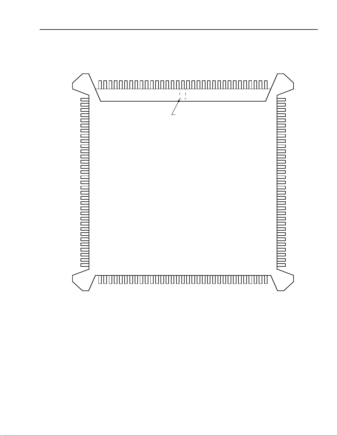
3 Pin Information
V
SSA
CKI
V
DDA
TDI
TDO
TMS
TCK
TRST
INT3
INT2
INT1
INT0
IACK
TRAP
V
DD
CKO
V
RSTB
STOP
READY
VEC0/IOBIT7
VEC1/IOBIT6
VEC2/IOBIT5
VEC3/IOBIT4
V
DD
IOBIT3
IOBIT2
IOBIT1
IOBIT0
DOEN2
DO2
OLD2
V
SS
AB2
AB1
AB0
V
15
16171413121110
18
19
20
21
22
23
24
25
26
27
28
29
30
31
32
33
SS
34
35
36
37
38
39
40
41
42
43
44
45
46
47
48
49
SS
50
53
52
51
5455565758596061626364656667686970717273747576777879808182
AB6
AB5
AB4
VDDAB3
987654321
AB9
AB8
VSSAB7
AB12
VDDAB11
AB10
PIN #1
IDENTIFIER
ZONE
DSP1620
132-PIN BQFP
VSSAB15
AB14
AB13
132
131
130
129
EXM
128
EROM
RWN
127
126
ERAMLO
125
ERAMHI
VDDERAMXIODB0
124
123
122
121
SS
DB1
DB2
V
119
118
117
120
116
115
114
113
112
111
110
109
108
107
106
105
104
103
102
101
100
83
V
DD
DB3
DB4
DB5
DB6
V
SS
DB7
DB8
DB9
DB10
V
DD
DB11
DB12
DB13
DB14
DB15
V
99
98
97
96
95
94
93
92
91
90
89
88
87
86
85
84
SS
OBE1
IBF1
DI1
ILD1
ICK1
OCK1
V
DD
OLD1
DO1
SYNC1
SADD1
DOEN1
PIDS
PCSN
PSTAT
V
SS
DD
V
ICK2
OCK2
OBE2
PB15
SS
DI2
V
IBF2
ILD2
DD
V
PB12
PB13
PB14
PB11
SS
V
PB7
PB8
PB9
PB10
PB6
PB5
PB4
DD
V
PB3
PB2
PB1
PB0
SS
V
POBE
PIBF
PODS
DD
V
PBSEL
5-4773(F)
Figure 1. DSP1620 132-Pin BQFP Pin Diagram (Top View)
Lucent Technologies Inc. 9
Page 12

Data Sheet
DSP1620 Digital Signal Processor June 1998
3 Pin Information
NU*
CKI
TDI
TDO
TMS
TCK
INT3
INT2
INT1
INT0
IACK
VDD
NU*
CKO
VSS
NU*
VDD
DO2
VSS
1
2
3
4
5
6
7
8
9
10
11
12
13
14
15
16
17
18
19
20
21
22
23
24
25
26
27
28
29
30
31
32
33
34
35
36
VSSA
VDDA
TRST
TRAP
RSTB
STOP
READY
VEC0/IOBIT7
VEC1/IOBIT6
VEC2/IOBIT5
VEC3/IOBIT4
IOBIT3
IOBIT2
IOBIT1
IOBIT0
DOEN2
OLD2
(continued)
VSS
NU*
AB0
AB1
AB2
AB3
VDD
AB4
AB5
AB6
AB7
VSS
AB8
AB9
AB10
AB11
VDD
AB12
AB13
AB14
AB15
NU*
VSS
NU*
EXM
RWN
EROM
ERAMLO
ERAMHI
VDD
ERAMXIODB0
DB1
144
143
142
141
140
139
138
137
136
135
134
133
132
131
130
129
128
127
126
125
124
123
122
121
120
119
118
117
116
115
114
113
112
111
DSP1620
144-PIN TQFP
37
3839404142434445464748495051525354555657585960616263646566676869707172
DB2
VSS
110
109
108
VDD
107
DB3
106
DB4
105
DB5
104
DB6
103
VSS
102
DB7
101
DB8
100
DB9
99
DB10
98
NU*
97
VDD
96
DB11
95
DB12
94
DB13
93
DB14
92
NU*
91
DB15
90
VSS
89
OBE1
88
IBF1
87
DI1
86
NU*
85
ILD1
84
ICK1
83
OCK1
82
VDD
81
OLD1
80
DO1
79
SYNC1
78
SADD1
77
DOEN1
76
PIDS
75
PCSN
74
PSTAT
73
VSS
NU*
DI2
VDD
ICK2
OCK2
VSS
ILD2
IBF2
PB15
OBE2
VDD
PB14
PB13
PB12
PB11
PB10
PB9
PB8
NU*
PB7
PB6
PB5
PB4
VSS
PB3
VDD
PB2
PB1
PB0
NU*
VSS
POBE
PIBF
VDD
PODS
PBSEL
5-4914 (f)
* NU = Not Usable; no external connections are allowed.
Figure 2. DSP1620 144-Pin TQFP Pin Diagram (Top View )
10 Lucent Technologies Inc.
Page 13

Data Sheet
June 1998 DSP1620 Digital Signal Processor
3 Pin Information
(continued)
Functional descriptions of BQFP pins 1—132 and TQFP pins 1—144 are found in Section 6, Signal Descriptions.
Input levels on all I (input) and I/O (input/output) type pins are designed to remain at full CMOS levels when not driven. At full CMOS levels, essentially no dc current is drawn. Although input and I/O buffers may be left untied, the
guidelines for terminating unused pins are as follows:
„
NC (no connect) pins should be left floating.
„
Input pins can either be tied directly to VSS or tied to VDD through a 10 kΩ resistor. Deciding VSS or VDD is important for input pins with special functions. For example, if the PHIF16 port is unused then the PCSN (PHIF16
Chip Select Not) pin should be tied high (no select).
„
Output pins should be left floating.
„
Bidirectional I/O pins configured as inputs should be tied to VDD or VSS through a 10 kΩ resistor. Bidirectional
I/O pins configured as outputs should be left floating. Bit I/O pins are programmed as inputs when the device is
reset (
sbit
= 0x00xx).
Do not directly connect them to V
SS or VDD
because of the output buffer.
Table 1. Pin Descriptions
BQFP Pin TQFP Pin Symbol Type Name/Function
101, 102, 103,
104, 105, 107,
108, 109, 110,
112, 113, 114,
115, 118, 119,
91, 93, 94, 95,
96, 99, 100,
101, 102, 104,
105, 106, 107,
110, 111, 112
DB[15:0]
*
External Memory Data Bus 15—0.
I/O
120
121 113 IO
124 116 ERAMHI
†
Data Address 0x8000 to 0x80FF I/O Enable.
O
†
Data Address 0xC000 to 0xFFFF External RAM En-
O
able.
125 117 ERAMLO
†
Data Address 0x8100 to 0xBFFF External RAM En-
O
able.
†
122 114 ERAMX
Data Address 0x8000 to 0xFFFF External RAM En-
O
able.
†
126 118 EROM
127 119 RWN
Program Address External ROM Enable.
O
†
Read/Write Not.
O
128 120 EXM I External ROM Enable.
130, 131, 132, 1,
3, 4, 5, 6, 8, 9,
10, 11, 13, 14,
15, 16
124, 125, 126,
127, 129, 130,
131, 132, 134,
135, 136, 137,
AB[15:0]
*
External Memory Address Bus 15—0.
O
139, 140, 141,
142
26, 27, 28, 29 10, 11, 12, 13 INT[3:0] I Vectored Interrupts INT3, INT2, INT1, and IN T0.
*
30 14 IACK
Interrupt Acknowledge.
O
36 22 STOP I STOP Input Clock (negative assertion).
37 23 READY I Processing Enable.
31 15 TRAP
*
Nonmaskable Program Trap/Breakpoint Indication.
I/O
35 20 RSTB I Reset (negative assertion).
33 18 CKO
†
Processor Clock Output.
O
24 8 TCK I JTAG Test Clock.
* 3-states when RSTB = 0 or by JTAG control.
† 3-stat es wh en the level of RST B = 0 and INT0 = 1 . Output = 1 when the level of R STB = 0 and INT0 = 0, except CKO which is free- running.
‡ 3-states by JTAG control.
§ Pull-up dev i ces on input.
** 3-states when RSTB = 0, JTAG control, or
†† For SIO multiprocessor applications, add 5 kΩ external pull-up resistors to SADD1 for proper initialization.
PHIFC
register bit PCFIG = 0.
Lucent Technologies Inc. 11
Page 14

Data Sheet
DSP1620 Digital Signal Processor June 1998
3 Pin Information
Table 1. Pin Descriptions
(continued)
(continued)
BQFP Pin TQFP Pin Symbol Type Name/Function
23 7 TMS
22 6 TDO
21 5 TDI
25 9 TRST
§
JTAG Test Mode Select.
I
‡
JTAG Test Data Output.
O
§
JTAG Test Data Input.
I
§
JTAG Test Reset (negative assertion).
I
19 3 CKI I Clock Input.
38 24 VEC0/IOBIT7
39 25 VEC1/IOBIT6
40 26 VEC2/IOBIT5
41 27 VEC3/IOBIT4
43 29 IOBIT3
44 30 IOBIT2
45 31 IOBIT1
46 32 IOBIT0
*
Vectored Interrupt Bit 0/BIO Signal Bit 7.
I/O
*
Vectored Interrupt Bit 1/BIO Signal Bit 6.
I/O
*
Vectored Interrupt Bit 2/BIO Signal Bit 5.
I/O
*
Vectored Interrupt Bit 3/BIO Signal Bit 4.
I/O
*
BIO Signal Bit 3.
I/O
*
BIO Signal Bit 2.
I/O
*
BIO Signal Bit 1.
I/O
*
BIO Signal Bit 0.
I/O
47 33 DOEN2 I SSIO Data Output Enable.
55 41 DI2 I SSIO Data Input.
53 39 ICK2
58 44 OBE2
56 42 IBF2
49 35 OLD2
54 40 ILD2
48 34 DO2
52 38 OCK2
88 77 DOEN1
89 78
SADD1
90 79 SYNC1
91 80 DO1
92 81 OLD1
94 83 OCK1
95 84 ICK1
96 85 ILD1
††
*
SSIO Input Clock.
I/O
*
SSIO Output Buffer Empty.
O
*
SSIO Input Buffer Full.
O
*
SSIO Output Load.
I/O
*
SSIO Input Load.
I/O
*
SSIO Data Output.
O
*
SSIO Output Clock.
I/O
*
SIO Data Output Enable.
I/O
*
SIO Multiprocessor Address.
I/O
*
SIO Multiprocessor Synchronization.
I/O
*
SIO Data Output.
O
*
SIO Output Load.
I/O
*
SIO Output Clock.
I/O
*
SIO Input Clock.
I/O
*
SIO Input Load.
I/O
97 87 DI1 I SIO Data Input.
*
98 88 IBF1
99 89 OBE1
59, 60, 61, 62, 64, 65,
66, 67
69, 70, 71, 72, 74, 75,
76, 77
79 68 POBE
80 69 PIBF
45, 46, 47, 48,
50, 51, 52, 53
57, 58, 59, 60,
62, 63, 64, 65
PB[15:8]
PB[7:0]
SIO Input Buffer Full.
O
*
SIO Output Buffer Empty.
O
**
PHIF16 Data Bus 15—8.
I/O
*
PHIF16 Data Bus 7—0.
I/O
*
PHIF16 Output Buffer Empty.
O
*
PHIF16 Input Buffer Full.
O
81 70 PODS I PHIF16 Output Data Strobe.
* 3-states when RSTB = 0, or by JTAG control.
† 3-states when the l evel of RSTB = 0 and INT0 = 1. Output = 1 when the level of RSTB = 0 and INT0 = 0, except CK O whi ch is free-running.
‡ 3-states by JTAG control.
§ Pull-up devices on input.
** 3-states when RSTB = 0, JTAG con trol, or
†† For SIO multiproc ess or applications, add 5 kΩ external pull-up resis tors to SAD D 1 for proper initializatio n.
PHIFC
regis t er bit PC FIG = 0.
12 Lucent Technologies Inc.
Page 15
Data Sheet
June 1998 DSP1620 Digital Signal Processor
3 Pin Information
Table 1. Pin Descriptions
(continued)
(continued)
BQFP Pin TQFP Pin Symbol Type Name/Function
87 76 PIDS I PH IF16 Input Data Strobe.
82 71 P BSEL I PHIF16 (8-bit external mode) Byte Select.
85 74 P STAT I PHIF16 Status Register Select.
86 75 PCSN I PHIF16 Chip Select Not.
7, 17, 34, 50, 57, 68, 78,
84, 100, 111, 117, 129
19, 36, 43, 56,
67, 73, 90, 103,
SS
V
P Ground.
109, 122, 133,
144
2, 12, 32, 42, 51, 63, 73,
83, 93, 106, 116, 123
16, 28, 37, 49,
61, 72, 82, 97,
DD
V
P Power Supply.
108, 115, 128,
138
20 4 V
18 1 V
— 2, 17, 21, 54,
55, 66, 86, 92,
DDA
SSA
P Analog Power Supply.
P Analog Ground.
NU — Not Usable (No external connections are
allowed.)
98, 121, 123,
143
* 3-states when RSTB = 0, or by JTAG control.
† 3-stat es wh en the level of RST B = 0 and INT0 = 1 . Output = 1 when the level of R STB = 0 and INT0 = 0, except CKO which is free- running.
‡ 3-states by JTAG control.
§ Pull-up dev i ces on input.
** 3-states when RSTB = 0, JTAG control, or
†† For SIO multiprocessor applications, add 5 kΩ external pull-up resistors to SADD1 for proper initialization.
PHIFC
register bit PCFIG = 0.
Lucent Technologies Inc. 13
Page 16

Data Sheet
DSP1620 Digital Signal Processor June 1998
4 Hardware Architecture
The DSP1620 device is a 16-bit, fixed-point, programmable digital signal processor (DSP). The DSP1620
consists of an enhanced DSP1600 core together with
on-chip memory and peripherals. Added architectural
features give the DSP1620 high program efficiency for
signal coding and I/O-intensive applications.
Throughout this manual, all DSP registers directly writable or readable by DSP instructions are printed in lower-case. I/O pins and nonprogram-accessible registers
are upper-case. All register names and DSP instructions are printed in
scriptions.
4.1 DSP1620 Archi tectural Overview
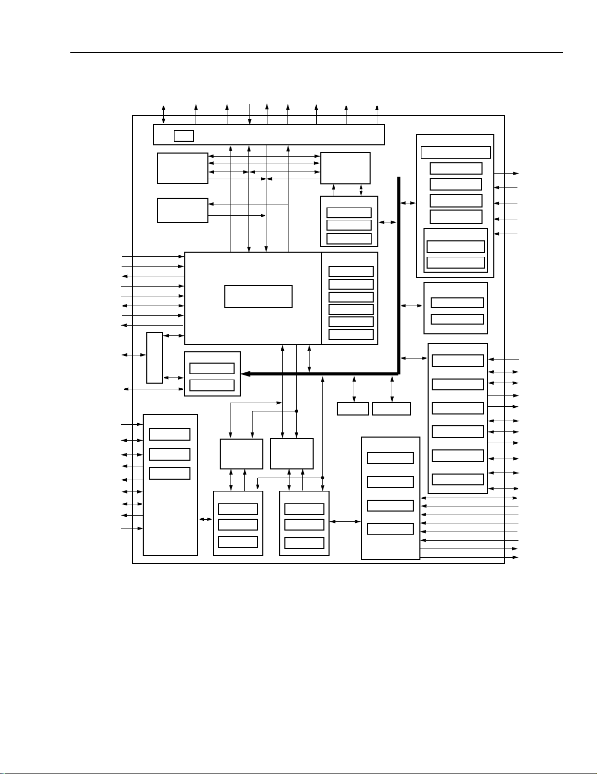
Figure 3 shows a block diagram of the DSP1620. The
following blocks make up this device.
DSP1600 Core
The DSP1600 core is the heart of the DSP1620 chip.
The core contains data and address arithmetic units,
and control for on-chip memory and peripherals. The
core provides support for external memory wait-states
and on-chip dual-port RAM and features vectored interrupts and a trap mechanism. The core is discussed further in Section 4.2.
Dual-Port RAM (DPRAM)
This block contains 30 banks (banks 1—30) of zero
wait-state memory. Each bank consists of 1K 16-bit
words and has separate address and data ports to the
instruction/coefficient and data memory spaces. A program can reference memory from either space. The
DSP1600 core automatically performs the requi red multiplexing. If references to both ports of a single bank are
made simultaneously, the DSP1600 core automati cally
inserts a wait-state and performs the data port access
first, followed by the instruction/coefficient port access.
A program can be downloaded from slow off-chi p memory into DPRAM, and then executed w ithout wait-states.
DPRAM is also useful for improving convolution performance in cases where the coefficients are adaptive.
Since DPRAM can be downloaded through the JTAG
port, full-speed, remote in-circuit emulation is possible.
DPRAM can also be used for downloading self-test
code via the JTAG port.
When the ECCP is active, DPRAM bank 30 is dedic ated
to the ECCP (for storing traceback information) and
cannot be accessed by the core.
boldface
when written in text de-
IORAM
IORAM storage consists of two 1 Kword banks (banks
31 and 32) of on-chip D PRAM that re si des i n the core ’s
internal data memory space. Each bank of IORAM has
two data and two address ports; an IORAM bank can be
shared with the core and a modular I/O unit (MIOU) to
implement a DMA-based I/O system. IORAM supports
concurrent core execution and MIOU I/O processing. If
both the core and MIOU simultaneously access the
same IORAM bank, the DSP1600 cor e automatically inserts a wait-state and performs the MIOU access first,
followed by the core access. MIOU IORAM requests
that do not collide with core IORAM requests do not incur a wait-sta te.
MIOU0 (controls SSIO) is attached to RAM bank 32;
MIOU1 (controls PHIF16) is attached to RAM bank 31.
Portions of IORAM not dedicated to I/O pr ocessing can
be used as general-purpose DPRAM in the data memory map.
Read-Only Memory (ROM)
The DSP1620 contains a 4 Kword boot ROM. The boot
routines are detailed in Section 7.
External Memory Interface (EMI)
The EMI is used to connect the DSP1620 to external
memory and I/O devices. It supports read/write operations from/to instruction/c oef ficient memor y (X memor y
space) and data memory (Y memory space). The
DSP1600 core automatically controls the EMI. Instructions can transparently reference external memory from
either set of internal bus es. A sequencer allows a s ingle
instruction to access both the X and the Y external
memory spaces.
Clock Synthesis
The DSP powers up with a 1X input clock (CKI) as the
source for the processor c lock. An on-chip clock s ynthesizer (PLL) can also be used to generate the system
clock for the DSP that runs at a frequency multiple of the
input clock. The clock synthesizer is deselected and
powered down on reset. For low-power operation, an internally generated slow clock can drive the DSP. If both
the clock synthesizer and the internally generated slow
clock are selected, the slow clock drives the DSP; however, the synthesizer continues to run.
The clock synthesizer and other programmable clock
sources are discussed in Section 4.16. The use of these
programmable clock sources for power management is
discussed in Section 4.17.
14 Lucent Technologies Inc.
Page 17

Data Sheet
June 1998 DSP1620 Digital Signal Processor
4 Hardware Architecture
Bit Manipulation Unit (BMU)
The BMU extends the DSP1600 core instruction set to
provide more efficient bit operations on accumulators.
The BMU contains logic for barrel shifting, normalization, and bit-field insertion/extr action. The uni t also c ontains a set of 36-bit alternate accumulators. The data in
the alternate accumulators can be shuffled with the data
in the main accumulators. Flags returned by the BMU
are testable by the DSP1600 conditional instructions.
Bit I/O Unit (BIO)
The BIO provides convenient and efficient monitoring
and control of eight individual ly configurable pins. When
configured as outputs, the pins can be individually set,
cleared, or toggled. When configured as inputs, individual pins or combinations of pins can be tested for patterns. Flags returned by the BIO mesh seamlessly with
conditional instructions.
(continued)
Serial I/O Unit (SIO)
The SIO offers an asynchronous, full-duplex, doublebuffered channel that operates at up to 25 Mbits/s (in a
nonmultiprocessor configuration), and easily interfaces
with other Lucent Technologies fixed-point DSPs in a
multiple-processor environment (mul tiprocessor mode).
Commercially available codecs and time-division multiplex (TDM) channels can be interfaced to the SIO with
few, if any, additional components.
In multiprocessor mode, an 8-bit serial protocol channel
can be transmitted in addition to the address of the
called processor. This feature is useful for transmitting
high-level framing information or for error detection and
correction.
Simple Serial I/O Unit (SSIO)
The SSIO offers an asynchronous, full-duplex, doublebuffered external channel that operates up to
25 Mbits/s. Commercially available codecs and timedivision multiplex channels can be interfaced to the
SSIO with few, if any, additional components. The SSIO
external interface is identical to the SIO external interface with the multiprocessor mode functionality and
SADD and SYNC signals deleted.
The SSIO is a DMA peripheral that interfaces di rectly to
the core’s data memory space under the control of
MIOU0.
Lucent Technologies Inc. 15
Page 18

Data Sheet
DSP1620 Digital Signal Processor June 1998
4 Hardware Architecture
Parallel Host Interface (PHIF16)
The PHIF16 is a passive 16-bit par allel port that can be
configured to interface to either an 8- or 16-bit external
bus containing other Lucent Technologies fixed point
DSPs (e.g., DSP1611, DSP1616, DSP1617, DSP1618,
DSP1620, DSP1627, DSP1628, DSP1629), microprocessors, or peripheral I/O devices. The PHIF16 port
supports either
When operating in the 16-bit external bus configuration,
PHIF16 can be programmed to swap high and low
bytes. When operating in 8-bit external bus configuration, PHIF16 is accessed in either an 8-bit or 16-bit logical mode. In 16-bit mode, the host selects either a high
or low byte access; in 8-bit mode, only the low byte is
accessed.
Additional software-programmable features allow for a
glueless host interface to microprocessors (see
Section 4.10, Parallel Host Interface (PHIF16)).
PHIF16 is a DMA peripheral and interfaces directly to
the core’s data memory space under the control of
MIOU1.
Timer
The timer can be used to provide an interrupt, either single or repetitive, at the expiration of a programmed interval. More than nine orders of magnitude of interval
selection are provided. The timer can be stopped and
restarted at any time.
JTAG and HDS Module
The on-chip Hardware Development System (HDS)
performs instruction breakpointing and branch tracing
at full speed without additional off-chip hardware. Using
the JTAG port, breakpointing is set up, and the trace
history is read back. The port works in conjunction with
the HDS code in the on-chip ROM and the hardware
and software in a remote computer.
A maximum of four hardware breakpoints can be set on
instruction addresses. A counter can be preset with the
number of breakpoints to receive before trapping the
core. Breakpoints can be set in interrupt service routines. Alternately, the counter can be preset with the
number of cache instructions to execute before trapping
the core.
Every time the program branches (rather than executing
the next sequential instruction) the addresses of the instructions executed before and after the branch are
Motorola
or
Intel
(continued)
protocols.
captured in circular memory. This memory contains the
last four pairs of program discontinuities for hardware
tracing.
In systems with multiple processors, the DSPs can be
configured so that any processor reaching a breakpoint
causes all the other processors to be trapped (see
Section 4.3, Interrupts and Trap).
Pin Multiplexing
Upon reset, the vectored interrupt indication signals,
VEC[3:0], are connected to the package pins while
IOBIT[4:7] are disconnected. Setting bit 12, EBIOH, of
ioc
the
pins, and disconnects VEC[3:0]. Note that VEC0 corresponds to IOBIT7, VEC1 corresponds to IOBIT6, VEC2
corresponds to IOBIT5, and VEC3 corresponds to
IOBIT4.
Power Management
Many applications, such as portable cellular terminals,
require programmable sleep modes for power management. There are three different control mechanisms for
achieving low-power operation: the
ister, the STOP pin, and the AWAIT bit in the
ter. The
saving modes by controlling internal clocks and peripheral I/O units. The STOP pin controls the internal processor clock. The AWAIT bit in the
the processor to go into a power-saving standby mode
until an interrupt occurs. The various power management options can be chosen based on power consumption and/or wake-up latency requirements.
Error Correction Coprocessor (ECCP)
The ECCP performs full Viterbi decoding with instructions for MLSE equalization and convolutional decoding. It is designed for 2-tap to 6-tap MLSE equalization
with Euclidean branch metrics and rate 1/1 to 1/6 convolutional decoding using constraining lengths from 2 to
7 with Euclidean or Manhattan branch metrics. Two
variants of soft-decoded symbols, as well as hard-decoded symbols, can be programmed. The ECCP operates in parallel with the DSP1600 core, increasing the
throughput rate. Single instruction Viterbi decoding provides significant code compression required for single
DSP solutions in modern digital cellular applications.
The ECCP is the source of two interrupts and one flag
to the DSP1600 core.
register connects IOBIT[4:7] to the package
powerc
powerc
register configures various power-
alf
control reg-
alf
regis-
register allows
16 Lucent Technologies Inc.
Page 19
Data Sheet
June 1998 DSP1620 Digital Signal Processor
4 Hardware Architecture
AB[15:0]DB[15:0]
ioc
DPRAM
1K x 16
BANKS 1—29
ROM
4K x 16
CKI
READY
CKO
RSTB
STOP
TRAP
INT[3:0]
IACK
IOBIT[7:4] /
VEC[3:0]
IOBIT[3:0]
DI2
ICK2
ILD2
IBF2
DO2
OCK2
OLD2
OBE2
DOEN2
M
U
X
SSIO
SSIOC*
SSDX(in)*
SSDX(out)*
BIO
sbit
cbit
(continued)
RWN EXM IO EROM ERAMHI ERAMLO
EXTERNAL MEMORY INTERFACE & EMUX
YAB YDB XDB XAB
DSP1600 C OR E
IORAM0
1K x 16
BANK 32
MIOU0
mcmd0
miwp0
morp0
ERAMX
YABYDB
IORAM1
1K x 16
BANK 31
MIOU1
mcmd1
miwp1
morp1
IDB
DPRAM
1K x 16
BANK 30
ECCP
eir
ear
edr
BMU
aa0
aa1
ar0
ar1
ar2
ar3
pllc
powerc
PHIF16
PHIFC*
PSTAT
PDX(in)*
PDX(out)*
BOUNDARY SCAN
†
JTAG
jtag
†
JCON
†
ID
†
BYPASS
HDS
BREAKPOINT
†
TRACE
TIMER
timerc
timer0
SIO
sdx(out)
srta
tdms
sdx(in)
sioc
saddx
†
TDO
TDI
TCK
TMS
TRST
†
DI1
ICK1
ILD1
IBF1
DO1
OCK1
OLD1
OBE1
SYNC1
SADD1
DOEN1
PB[15:0]
PIDS
PODS
PCSN
PBSEL
PSTAT
POBE
PIBF
* These registers are accessible through the MIOU command registers (mcmd0 and mcmd1).
† These registers are accessible through external pins only.
5-4142(F).e
Figure 3. DSP1620 Block Diagram
Lucent Technologies Inc. 17
Page 20

Data Sheet
DSP1620 Digital Signal Processor June 1998
4 Hardware Architecture
(continued)
Table 2. DSP1620 Block Diagram Legend
Symbol Name
aa<0—1> Alternate Accumulators.
ar<0—3> Auxiliary BMU Registers.
BIO Bit I/O Unit.
BMU Bit Manipulation Unit.
BREAKPOINT Four Instruction Breakpoint Registers.
BYPASS JTAG Bypass Register.
cbit BIO Control Register.
DPRAM Dual-Port Random Access Memory.
ECCP Error Correction Coprocessor.
ear ECCP Address Register.
edr ECCP Data Register.
eir ECCP Instruction Register.
EMUX External Memory Multiplexer.
HDS Hardware Development System.
ID JTAG Device Identification Register.
IDB Internal Data Bus.
ioc I/O Configuration Register.
IORAM0 Bank 32 of Internal Data RAM: Shared with MIOU0.
IORAM1 Bank 31 of Internal Data RAM: Shared with MIOU1.
JCON JTAG Configuration Registers.
JTAG JTAG Test Access Port.
jtag 16-bit Serial/Parallel Register.
MIOU0 Modular I/O Unit 0: Controls SSIO.
mcmd0 MIOU0 Command Register.
miwp0 MIOU0 IORAM 0 Input Data Write Pointer.
morp0 MIOU0 IORAM0 Output Data Read Pointer.
MIOU1 Modular I/O Unit 1: Controls PHIF16.
mcmd1 MIOU1 Command Register.
miwp1 MIOU1 IORAM 1 Input Data Write Pointer.
morp1 MIOU1 IORAM1 Output Data Read Pointer.
MUX Multiplexer.
PHIF16 16-bit Parallel Host Interface.
PDX(in) PHIF16 Input Data Register.
PDX(out) PHIF16 Output Data Register.
PHIFC Parallel Host Interface Control Register: Programmed Through MIOU1.
pllc Phase-Locked Loop Control Register.
powerc Power Control Register.
PSTAT Parallel Host Interface Status Register.
ROM Internal ROM.
saddx SIO Multiprocessor Protocol Register.
sbit BIO Status Register.
sdx(in) Serial Data Transmit Input Register.
sdx(out) Serial Data Transmit Output Register.
SIO Serial I/O Unit.
sioc Serial I/O Control Register.
srta Serial Receive/Transmit Address Register.
SSIO Simple Serial I/O Unit.
SSIOC Serial I/O Control Register for SSIO: Programmed Through MIOU0.
18 Lucent Technologies Inc.
Page 21
Data Sheet
June 1998 DSP1620 Digital Signal Processor
4 Hardware Architecture
(continued)
Table 2. DSP1620 Block Diagram Legend
Symbol Name
SSDX(in) I/O Data Input Register.
SSDX(out) I/O Data Output Register.
tdms Serial I/O Time-Division Multiplex Signal Control Register.
TIMER Programmable Timer.
timer0 Timer Running Count Register.
timerc Timer Control Register.
TRACE Program Discontinuity Trace Buffer.
XAB Program Memory Address Bus.
XDB Program Memory Data Bus.
YAB D ata Memory Address Bus.
YDB Data Memory Data Bus.
(continued)
Lucent Technologies Inc. 19
Page 22

Data Sheet
DSP1620 Digital Signal Processor June 1998
4 Hardware Architecture
(continued)
4.2 DSP1600 Core A rc hitectural Overview
Figure 4 shows a block diagram of the DSP1600 core.
System Cache and Control Section (SY S)
This section of the core c ontains a 15-word cac he memory and controls the instruction sequencing. It handles
vectored interrupts and traps, and also provides decoding for registers outside of the DSP1600 core. SYS
stretches the processor cycl e if wai t-states are r equired
(wait-states are programmable for external memory accesses). SYS also sequences downloading via JTAG of
self-test programs to on-chip dual-port RAM.
The cache loop iteration count can be specified at run
time under program control as well as at assembly time.
Data Arithmetic Unit (DAU)
The data arithmetic unit (DAU) contains a 16 x 16-bit
parallel multiplier that generates a full 32-bit product in
one instruction cycle. The product can be accumulated
with one of two 36-bit accumulators. The accumulator
data can be directly loaded from, or stored to memory in
two 16-bit words with optional saturation on overflow.
The arithmetic logic unit (ALU) supports a full set of
arithmetic and logical operations on either 16- or 32-bit
data. A standard set of flags can be tested for conditional ALU operations, branches, and s ubroutine calls. This
procedure allows the processor to perform as a powerful 16- or 32-bit microprocessor for logical and control
applications. The available instruction set is fully compatible with the DSP1627 instruction set. See Section
5.1 for more information on the instruction set.
The user also has access to two additional DAU registers. The
the DAU (see Table 46, psw — Processor Status Word
Register). The arithmetic control register,
to configure some of the features of the D AU (see Table
35) including single-cycle squaring. The
alignment field supports an arithmetic shift left by one
and left or right by two. The
reset.
The counters c0, c1, and c2 are signed, 8 bits wide, and
are used to count events such as the number of times
the program has executed a sequence of code. They
are controlled by the conditional instructions and provide a second convenient method of program looping.
psw
register contains status information from
auc
auc
auc
register is cleared by
, is used
register
Y Space Address Arithmetic Unit (YAAU)
The YAAU supports high-speed, register-indirect, compound, and direct addressing of data (Y) memor y. Four
general-purpose 16-bit registers, r0 to r3, are available
in the YAAU. These registers can be used to supply the
read or write addresses for Y space data. The YAAU
also decodes the 16-bit data memory address and outputs individual memory enables for the data access.
The YAAU can address the thirty-two 1 Kword banks of
on-chip DPRAM/IORAM and a maximum of 128 Kwords
of external storage.
Two 16-bit registers, rb and re, allow zero-overhead
modulo addressing of data for efficient filter implementations. Two 16-bit signed registers, j and k, are used to
hold user-defined postmodification increments. (k is
used only for c ompound address ing.) Fix ed i ncrements
of +1, –1, and +2 are also avail able. Four compound addressing modes are provided to make r ead/wri te operations more efficient.
The YAAU allows direct (or indexed) addressing of data
memory. In direct addressing, the 16-bit base register
ybase
(
dress. The direct data instruction supplies the remaining
5 bits to form an address to Y memory space and also
specifies one of 16 registers for the source or destination.
X Space Address Arithmetic Unit (XAAU)
The XAAU supports high-speed, register-indirect, instruction/coefficient memory addressing with postmodification of the register. The 16-bit pt register is used for
addressing coefficients. The 16-bit signed register i
holds a user-defined postincrement. A fixed postincrement of +1 is also av ailable. Register PC i s the program
counter and is not directly ac cessible by the user. 16-bit
registers pr and pi hold the return address for subroutine calls and interrupts, respectively.
The XAAU decodes the 16-bit instruction/coefficient address and produces enable signals for the appropriate
X memory segment. Addressable instruction/coefficient
segments include on-chip IROM, 30 Kwords on-chip
DPRAM, and 64 Kwords of external storage. The locations of these memory segments depend upon the
memory map selected (see Table 5, Instruction/Coefficient Memory Maps).
) supplies the 11 most significant bits of the ad-
20 Lucent Technologies Inc.
Page 23
Data Sheet
June 1998 DSP1620 Digital Signal Processor
4 Hardware Architecture
CONTROL
ins (16)
inc (16)
p (32)
yh (16)
yl (16)
32
x (16)
16 x 16 MPY
SHIFT (–2, 0, 1, 2)
(continued)
CACHE
cloop (7)
alf (16)
mwait (16)
DAU
SYS
ADDER
PC (16)
pt (16)
i (16)
j (16)
k (16)
MUX
1
pr (16)
pi (16)
MUX
XAAU
BRIDGE
–1, 0, 1, 2
XDB
XAB
IDB
YDB
YAAU
MUX
ALU/SHIFT
a0 (36)
a1 (36)
16
EXTRACT/SAT
ADDER
36
c0 (8)
c1 (8)
c2 (8)
auc (16)
psw (16)
re (16)
CMP
ybase (16)
Figure 4. DSP1600 Core Block Diagram
YAB
rb (16)
MUX
r0 (16)
r1 (16)
r2 (16)
r3 (16)
5-1741(F).b
Lucent Technologies Inc. 21
Page 24

Data Sheet
DSP1620 Digital Signal Processor June 1998
4 Hardware Architecture
(continued)
Table 3. DSP1600 Core Block Diagram Legend
Symbol Name
16 x 16 MPY 16-bit x 16-bit Multiplier.
a0—a1
Accumulators 0 and 1 (16-bit halves specified as a0,
alf AWAIT, LOWPR, F lags.
ALU/SHIFT Arithmetic Logic Unit/Shifter.
auc Arithmetic Unit Control.
c0—c2 Counters 0—2.
cloop Cache Loop Count.
CMP Comparator.
DAU Data Arithmetic Unit.
EXTRACT/SAT Extract/Saturate.
i Increment Register for the X Address Space.
IDB Internal Data Bus.
inc Interrupt Control Register.
ins Interrupt Status Register.
j Increment Register for the Y Address Space.
k Increment Register for the Y Address Space.
MUX Multiplexer.
mwait External Memory Wait-States Register.
p Product Register.
PC Program Counter.
pi Pr ogram Interrupt Return Register.
pr Program Return Register.
psw Pr o cessor Status W o rd.
pt X Address Space Pointer.
r0—r3 Y Address Space Pointers.
rb Modulo Addressing Register (begin address).
re Modulo Addressing Register (end address).
SYS System Cache and Control Section.
x Multiplier Input Register.
XAAU X Space Add re ss Arithmetic Un it.
XAB X Space Address Bus.
XDB X Space Data Bus.
y DAU Register.
YAAU Y Space Add re ss Arithmetic Un it.
YAB Y Space Address Bus.
YDB Y Space Data Bus.
ybase Direct Addressing Base Register.
* F3 ALU instructions with immediates require specifying the high half of the accumulators as
a0l, a1
a0h
and
, and
a1h
*
a1l
.
)
.
22 Lucent Technologies Inc.
Page 25

Data Sheet
June 1998 DSP1620 Digital Signal Processor
4 Hardware Architecture
(continued)
4.3 Interrupts and Trap
The DSP1620 supports prioritized, vectored interrupts
and a trap. The device has eleven internal hardware interrupt sources and four external interrupt pins. Additionally, there is a trap pin and a trap signal from the
hardware development system (HDS). A software i nterrupt is available through the
instruction is reserved for use by the HDS. Each of
these sources of interrupt and trap has a unique vector
address and priority assigned to it.
The software interrupt and the traps are always enabled
and do not have a corresponding bit in the
Other vectored interrupts are enabled in the
(see Table 39, inc — Interrupt Control Register) and
monitored in the
rupt Status Register). When the DSP1620 goes into an
interrupt or trap service routine, the IACK pin is asserted. In addition, pins VEC[3:0] encode which interrupt/
trap is being serviced. Table 4 details the encoding
used for VEC[3:0].
The DSP1620 WAKEUP interrupt is a new source of
core interrupt. WAKEUP is triggered by the logical OR
of the PHIF16 input buffer full flag and the SSIO input
buffer full flag. The purpose of this interrupt is to reactivate sleeping MIOUs (
peripheral input processing.
Interruptibility
Vectored interrupts are serviced only after the execution
of an interruptible instruction. If more than one
vectored interrupt is asserted at the same time, the interrupts are serviced sequentially according to their assigned priorities. S ee Table 4 for the priorities assigned
to the vectored interrupts. Interrupt service routines,
branch and conditional branch instructions, cache
loops, and instructions that only decrement one of the
RAM pointers, r0 to r3 (e.g., *
ible.
A trap is similar to an interr upt, but it gains control of the
processor by branching to the trap service routine even
when the current instruction i s noninterruptible. It might
not be possible to return to normal ins truction execution
from the trap service routine because the machine state
cannot always be saved. In particular, program execution cannot be continued from a trapped cache loop or
interrupt service routine. While in a trap service routine,
another trap is ignored.
ins
register (see Table 40, ins — Inter-
icall
instruction. The
ins
alf
AWAIT bit set) and resume
r3
− −
), are not interrupt-
register.
inc
register
icall
When set to 1, the status bits in the
that an interrupt has occurred. The processor must
reach an interruptible state (completion of an interruptible instruction) before an enabled vectored interrupt is
acted on. An interrupt is not serviced if it is not enabled.
Polled interrupt service can be implemented by disabling the interrupt in the
ins
the
register for the expected event.
Vectored Interrupts
Tables 39 and 40 show the
1 written to any bit of
sociated interrupt. If the bit is cleared to a logic 0, the interrupt is masked. Note that neither the software
interrupt nor traps can be masked.
The occurrence of an interrupt that is not masked causes the program execution to transfer to the memory location pointed to by that interrupt's vector address,
assuming no other interrupt is being serviced (see Ta-
ble 4). The occurrence of an interrupt that is masked
causes no automatic processor action, but sets the c orresponding status bit in the
terrupt occurs, it is latched in the
interrupt is not taken. When unlatched, this latched interrupt initiates automatic processor interrupt action.
See the
Manual for a more detailed description of the interrupts.
Signaling Interrupt Service Status
Five pins of DSP1620 are devoted to signaling interr upt
service status. The IACK pin goes high while any interrupt or user trap is being serviced, and goes low when
the ireturn instruction from the servic e routine is issued.
Four pins, VEC[3:0], carry a code indicating which of the
interrupts or trap is being serviced. Table 4 contains the
encodings used by each interrupt.
Traps due to HDS breakpoints have no effect on either
the IACK or VEC[3:0] pins. Instead, they show the interrupt state or interrupt source of the DSP when the trap
occurred.
DSP1620 Digital Signal Processor
inc
inc
inc
enables (or unmasks) the as-
ins
ins
register indicate
register and then polling
ins
and
registers. A logi c
register. If a masked in-
ins
register, but the
Information
Lucent Technologies Inc. 23
Page 26

Data Sheet
DSP1620 Digital Signal Processor June 1998
4 Hardware Architecture
Table 4. Interrupt Vectors
Source Vector Priority VEC[3:0] Issued by
No Interrupt — — 0x0 —
Software Interrupt 0x2 1 0x1 icall
INT0 0x1 2 0x2 INT0 pin
JINT 0x42 3 0x8 jtag pin
INT1 0x4 4 0x9 INT1 pin
INT2 0x8 5 0xa INT2 pin
INT3 0xc 6 0xb INT3 pin
TIME 0x10 7 0xc timer
MIBF0 0x14 8 0xd MIOU0 (SSIO )
MOBE0 0x18 9 0xe MIOU0 (SSIO)
WAKEUP 0x1c 10 0x0 SSIO or PHIF16 input buffer full
EREADY 0x20 11 0x1 ECCP ready
EOVF 0x24 12 0x2 ECCP overflow
IBF 0x2 c 14 0x3 SIO in
OBE 0x30 15 0x4 SIO out
MIBF1 0x34 16 0x5 MIOU1 (PHIF16)
MOBE1 0x38 17 0x6 MIOU1 (PHIF16)
TRAP from HDS 0x3 18
TRAP from User 0x46 19 = highest 0x7 pin
* Traps due to HDS breakpoints have no effect on VEC[3:0] pins.
(continued)
—*
breakpoint, jtag, or pin
Clearing Interrupts
MIOU-reported SSIO and PHIF16 interrupts (MIBF0, MOBE0, MIBF1, MOBE1) are cleared by writing the reporting
MIOU’s command register with the appropriate length update command. See Section 4.8.
The SIO interrupts (IBF, OBE) are cleared one instruction cycle after reading or writing, as appropriate, the serial
data registers
nop
tion (
terrupt service routine (via
reported following an ireturn.
The JTAG interrupt (JINT) is cleared by reading the
Eight of the vectored interrupts can be cleared by writing to the
INT3, TIME, EREADY, EOVF, or WAKEUP bits in the
cleared to a logic 0. The status bit for these vectored interrupts is also cleared when the ireturn instruction is executed, leaving set any other vectored interrupts that are pending.
sdx
(in), and
or other) follows the
sdx
(out). To account for this latency, the programmer shoul d ensure that a single i nstruc-
sdx
read/write instruction before examining the
ireturn
). This ensures that stale flags are not read or that an erroneous interrupt is not
jtag
register.
ins
register. Writing a 1 to the INT0, INT1, INT2,
ins
will cause the corresponding interrupt status bit to be
ins
register or prior to leaving an in-
24 Lucent Technologies Inc.
Page 27

Data Sheet
June 1998 DSP1620 Digital Signal Processor
4 Hardware Architecture
Traps
The TRAP pin of the DSP1620 is a bidirectional signal.
At reset, it is configured as an input to the processor.
Asserting the TRAP pin forces a user trap. Once the
trap pin is asserted, it must remain asserted until
VEC[3:0] is 0xd (acknowledgment). The trap mechanism is used for two purposes: by an application to rapidly gain control of the processor for asynchronous timecritical event handling (typical ly for catastrophic error recovery). It is also used by the HDS for breakpointing
and gaining control of the processor. Separate vectors
are provided for the user trap (0x46) and the HDS trap
(0x3). Traps are not maskable.
A trap has four cycles of latency. At most, two instructions execute from the time the trap is received at the
pin to when it gai ns control. An instruction that is exec uting when a trap occurs is allowed to complete before the
trap service routine is entered. (Note that the instruction
could be lengthened by wait-states.) During normal program execution, the pi register contains either the address of the next instruction (two-cycle instruction
executing) or the address following the next instruction
(one-cycle instruction executing). In an interrupt service
routine, pi contains the interrupt return address. When
a trap occurs during an interrupt servi ce routine, the value of the pi register is overwritten. Specifically, it is not
possible to return to an interrupt service routine from a
user trap (0x46) service routine. Also, continuing program execution when a trap occurs during a c ache loop
is not possible.
The HDS trap causes circuitry to force the program
memory map to XMAP1 (with on-chip ROM starting at
address 0x0) when the trap is taken. The previous
memory map is restored when the trap service routine
exits by issuing an i return. The map is forced to XMA P1
because the HDS code resides in the on-chip ROM.
(continued)
Wait for Interrupt (Standby or Sleep Mode)
The DSP1620 has a power-saving standby mode in
which the internal processor clock stretches indefinitely
until the core receives an interrupt or trap request. A
minimum amount of core circuitry remains active in
order to process the incoming interrupt. The clocks to
the peripherals are unaffected and the peripherals continue to operated during standby mode. The program
places the core in standby mode by setting the AWAIT
bit (bit 15) of the
AWAIT bit is set, one additional instruction is executed
before the standby mode is entered. When an interrupt
occurs, core hardware resets AWAIT, and normal core
processing is resumed.
The MIOUs remain operational even in standby mode.
Their clocks remains running and they continue any
DMA activity.
nop
Two
AWAIT bit is set. The first
before sleeping; the second is executed after the interrupt signal awakens the DSP and before the interrupt
service routine is executed.
The AWAIT bit should be set from within the cache if the
code that is executing resides in external program
memory where more than one wait-state has been programmed. This ensures that an interrupt does not disturb the device from completely entering the sleep state.
For additional power savings, in addition to setting
the value 0x8000, set
erc
shuts down the timer and prescaler (see Table 54 and
Table 41).
Power consumption can be further reduced by by activating other available low-power modes. See Power
Management beginning on page 71 for information on
these other modes.
instructions should be programmed after the
to the value 0x0040. This holds the CKO pin low and
alf
register (
alf
= 0x8000). After the
nop
(one cycle) is executed
ioc
to the value 0x0180 and
alf
to
tim-
Using the Lucent Technologies development tools, the
TRAP pin can be configured to be an output or an input
vectoring to address 0x3. In a multiprocessor environment, the TRAP pins of all the DSPs present can be tied
together. During HDS operations, one DSP is selected
by the host software to be the master. The master processor's TRAP pin is configured to be an output. The
TRAP pins of the slave processors are configured as inputs. When the master processor reaches a breakpoint,
the master's TRAP pin is asserted. The slave processors respond to their TRAP input by beginning to execute the HDS code.
Lucent Technologies Inc. 25
Page 28

Data Sheet
DSP1620 Digital Signal Processor June 1998
4 Hardware Architecture
(continued)
4.4 Memory Maps and Wait-States
The DSP1600 core implements a modified Harvard architecture that has separate on-chip 16-bit address and
data buses for the instruction/coefficient (X) and data
(Y) memory spaces. The DSP1620 provides a multiplexed external bus that accesses external RAM
(ERAM), ROM (EROM), and memory-mapped I/O
space (I/O). Programmable wait-states are provided for
external accesses.
Both the instruction/coefficient memory space and data
memory space are configurable to provide application
flexibility.
Table 5 shows the DSP1620 instruction/coefficient
memory space maps including the values for the external ROM enable pin (EROM) and address range of the
external memory interface address bus (AB).
Table 6 shows the DSP1620 data memory space in-
cluding values for the EROM, ERAMHI, ERAMLO,
ERAMX, IO, and AB external memory interface pins.
Instruction/Coefficient Memory Map Selection
Three parameters are used to select the active instruction/coefficient memory map: LOWPR, EXTROM, and
EXM.
The LOWPR bit of the
tomatically at reset. LOWPR controls the starting address of the thirty 1K banks of DPRAM. If LOWPR is
low, DPRAM begins at address 0x8000. If LOWPR is
high, DPRAM begins at address 0x0. IROM is not visible when LOWPR is asserted.
When LOWPR is asserted, the EXTROM bit of the
register determines which 32K segment of a possible
64K EROM physical address s pace is vis ible to the programmer. If EXTROM is asserted, physi cal EROM locations 0x0—0x7FFF are visible in the logical address
space 0x8000—0xFFFF. If EXTROM is deasserted,
physical EROM locations 0x8000—0xFFFF are visible
in the logical address space 0x8000—0xFFFF.
If LOWPR is deasserted, the value of the EXM pin at reset determines whether the internal 4 Kwords ROM
(IROM) or EROM locations 0x0—0x7FFF are addressable in the address range 0x0—0x7FFF.
The Lucent Technologies development system tools,
together with the on-chip HDS circuitry and the JTAG
port, can independently set the memory map. Specifically, during an HDS trap, the memory map is forced to
XMAP1. The user's map selection is r estored when the
trap service routine has completed execution.
alf
register is initialized to 0 au-
ioc
26 Lucent Technologies Inc.
Page 29

Data Sheet
June 1998 DSP1620 Digital Signal Processor
4 Hardware Architecture
(continued)
XMAP1
XMAP1 has IROM starting at 0x0 and 30 Kwords of DPRAM starting at 0x8000. XMAP1 is established if DSP1620
has EXM low at reset and the LOWPR parameter is programmed to zero. XMAP1 is also used during an HDS trap.
XMAP2
XMAP2 has 32 Kwords of external ROM (physical EROM addresses 0x0000—0x7FFF) starting at address 0x0. A s
in XMAP1, 30 Kwords of DPRAM begins at address 0x8000.
XMAP3
XMAP3 has 30 Kwords of DPRAM starting at address 0x0. 32 Kwords of EROM (physical EROM addresses
0x8000—0xFFFF) storage begins at 0x8000.
XMAP4
XMAP4 has 30 Kwords of DPRAM starting at address 0x0. 32 Kwords of EROM (physical EROM addresses
0x0000—0x7FFF) storage begins at 0x8000.
Table 5. Instruction/Coefficient Memory Maps
*
†
EXTROM = X
‡
LOWPR = 0
XMAP2
EXM = 1
EXM = X
†
EXTROM = 0
LOWPR = 1
XMAP3
§
EXM = X
§
EXTROM = 1
LOWPR = 1
XMAP4
X Address
XMAP1
EXM = 0
EXTROM = X
LOWPR = 0
0x0000—0x0FFF
0x1000—0x77FF
0x7800—0x7FFF
0x8000—0xF7FF
0xF800—0xFFFF
* MAP1 is set automatically during an HDS trap. The user-selected map is restored at the end.
† EXTROM is a don’ t care when LOWPR is d easser ted.
‡LOWPR is
memo ry map.
§ EXM is a don’t care when LOWPR is asserted.
alf
regis ter bit 14. The Lucent Technologi es development s ystem tool s c an i ndependently se t the
IROM
(4K)
EROM = 1
RESERVED
EROM
(32K)
EROM = 0
AB = 0x0000—
0x7FFF
DPRAM
(30K)
EROM = 1
DPRAM
(30K)
EROM = 1
RESERVED RESERVED
DPRAM
(30K)
EROM = 1
EROM = 1
RESERVED RESERVED
EROM
(32K)
EROM = 0
AB = 0x8000—
0xFFFF
EROM = 0
AB = 0x0000—
0x7FFF
DPRAM
(30K)
EROM
(32K)
Lucent Technologies Inc. 27
Page 30

Data Sheet
DSP1620 Digital Signal Processor June 1998
4 Hardware Architecture
Boot from External ROM
After RSTB goes from low to high, the DSP1620 comes
out of reset and fetches an instruction from address
zero of the instruction/coefficient space. The physical
location of address zero is determined by the memory
map in effect. If EXM is high at the rising edge of RSTB,
XMAP2 is selected. XMAP2 has EROM at location zero;
thus, program execution begins from external memory.
If EXM is high and INT1 is low when RSTB rises, the
mwait
register defaults to 15 wai t-states for all external
memory segments. If INT1 is high, the
defaults to 0 wait-states.
Data Memory Map Selection
Data memory map selection is based upon the value of
the EXTROM and WEROM
YMAP1
In YMAP1, the programmer can access 32 Kwords of
DPRAM (logical address 0x0000—0x7FFF), and the
most significant half of the 64 Kwords physical ERAM
space.
(continued)
ioc
register bits.
mwait
register
YMAP2
In YMAP2, the programmer can access 32 Kwords of
DPRAM (logical address 0x0000—0x7FFF), and the
least significant half of the 64 Kwords physical ERAM
space.
YMAP3
In YMAP3, the programmer can access 32 Kwords of
DPRAM (logical address 0x0000—0x7FFF), and the
most significant half of the 64 Kwords physical EROM
space.
YMAP4
In YMAP4, the programmer can access 32 Kwords of
DPRAM (logical address 0x0000—0x7FFF), and the
least significant half of the 64 Kwords physical EROM
space.
28 Lucent Technologies Inc.
Page 31

Data Sheet
June 1998 DSP1620 Digital Signal Processor
4 Hardware Architecture
Table 6. Data Memory Maps
YMAP 1
Y Address
0x0000—0x7FFF
0x8000—0x80FF
0x8100—0xBFFF
0xC000—0xFFFF
EXTROM = 0
WEROM = 0
DPRAM
(32K)
EROM = 1
ERAMHI = 1
ERAMLO = 1
ERAMX = 1
IO = 1
I/O
(0.25K)
EROM = 1
ERAMHI = 1
ERAMLO = 1
ERAMX = 0
IO = 0
AB = 0x8000—
0x80FF
ERAMLO
(15.75K)
EROM = 1
ERAMHI = 1
ERAMLO = 0
ERAMX = 0
IO = 1
AB = 0x8100—
0xBFFF
ERAMHI
(16K)
EROM = 1
ERAMHI = 0
ERAMLO = 1
ERAMX = 0
IO = 1
AB = 0xC000—
0xFFFF
(continued)
YMAP 2
EXTROM = 1
WEROM = 0
DPRAM
(32K)
EROM = 1
ERAMHI = 1
ERAMLO = 1
ERAMX = 1
IO = 1
(0.25K)
EROM = 1
ERAMHI = 1
ERAMLO = 1
ERAMX = 0
IO = 0
AB = 0x0000—
0x00FF
ERAMLO
(15.75K)
EROM = 1
ERAMHI = 1
ERAMLO = 0
ERAMX = 0
IO = 1
AB = 0x0100—
0x3FFF
ERAMHI
(16K)
EROM = 1
ERAMHI = 0
ERAMLO = 1
ERAMX = 0
IO = 1
AB = 0x4000—
0x7FFF
I/O
YMAP 3
EXTROM = 0
WEROM = 1
DPRAM
(32K)
EROM = 1
ERAMHI = 1
ERAMLO = 1
ERAMX = 1
IO = 1
EROM
(32K)
EROM = 0
ERAMHI = 1
ERAMLO = 1
ERAMX = 1
IO = 1
AB = 0x8000—
0xFFFF
YMAP 4
EXTROM = 1
WEROM = 1
DPRAM
(32K)
EROM = 1
ERAMHI = 1
ERAMLO = 1
ERAMX = 1
IO = 1
EROM
(32K)
EROM = 0
ERAMHI = 1
ERAMLO = 1
ERAMX = 1
IO = 1
AB = 0x0000—
0x7FFF
Wait-States
The number of wait-states (from 0 to 15) used when accessing each of the four external memory segments
(ERAMLO, I/O, ERAMHI, and EROM) is programmable in the
references memory in one of the four external segments, the internal multiplexer is automatically switched to the
appropriate set of internal buses, and the associated external enable of ERAMLO, I/O, ERAMHI, or EROM is issued.
The external memory cycl e is automatically stretched by t he number of wait-states configured i n the appropriate field
mwait
of the
and I/O fields of
Lucent Technologies Inc. 29
register. When ERAMX is used to enable the single 64K external segment, the ERAMLO, ERAMHI,
mwait
must be programmed to reflect the segment’s wait-state requirement.
mwait
register (see Table 42). When the program
Page 32

Data Sheet
DSP1620 Digital Signal Processor June 1998
4 Hardware Architecture
(continued)
4.5 External Memo ry Inter face (EMI)
The external memory interface supports read/write operations from instruction/coefficient memory, data
memory, and memory-mapped I/O devices. The
DSP1620 provides a 16-bit external address bus,
AB[15:0], and a 16-bit external data bus, DB[15:0].
These buses are multiplexed between the internal buses for the instruction/coefficient memory and the data
memory. Five external memory segment enables, ERAMLO, ERAMX, ERAMHI, IO, and EROM, select the
external memory segment to be addressed. Table 5 and
Table 6 describe the functionality of these bits.
The ERAMHI, ERAMLO, ERAMX, and IO external
memory interface pins provi de flexi bility in mapping the
64 Kwords YMAP1 and YMAP2 external data memory
(Y) space. ERAMHI enables a single 32 Kwords physical segment; ERAMLO enables a single 32 Kwords
physical segment with two 256 w ord holes all ocated for
memory-mapped I/O (I/O). ERAMX enables a single
64 Kwords physical memory segment (composed of the
entire address range described by ERAMLO, ERAMHI,
and I/O). ERAMHI, ERAMLO, ERAMX, and I/O seg-
ments exist only in the Y address space.
The EROM segment enable maps a single 64 Kwords
physical memory segment that can be addressed from
either the X or Y address spaces.
Two possible external system configurations are shown
in Figure 5 and Figure 6. Figure 5 illustrates a system
constructed from 32K x 16 and 64K x 16 SRAM devices.
ERAMHI and ERAMLO segments are assigned individual 32K x 16 SRAM chips; the EROM segment is assigned a single 64K x 16 device. 512 ERAMLO
locations are dedicated to the 256 dev ice I/O spa ce and
cannot be accessed by software.
*
Writes to the I/O space als o w rite the corresponding addresses in ERAMX storage; therefore, ERAMX locations that correspond to I/O-space write locations
actually used by the software (possibly less than 256 locations) cannot be used for general-purpose data storage. (They will always hold the last value wri tten to their
corresponding I/O write address.)
The flexibility provided by the programmable opti ons of
the external memory interface (see Table 41 and
Table 42) allows the DSP1620 to interface gluelessly
with a variety of commercially available memory chips.
Each of the four external memory segments (ERAMLO,
I/O, ERAMHI, and EROM) has a number of wait-states
that are programmable (from 0 to 15) by writing to the
mwait
register. When the program references memory
in one of the four external segments, the internal multiplexer is automatically sw itched to the appropr iate set of
internal buses, and the associated external enable of
the segment is issued. The external memory cycle is
automatically stretched by the number of wait-states in
the appropriate field of the
mwait
register.
When ERAMX is used to enable the single 64K external
segment, the ERAMLO, ERAMHI, and I/O fields of
mwait
are used to define the memory wait-state re-
quirements for each region of the unified 64K space.
When writing to external memory, the RWN pin goes
low for the external cycle. The external data bus,
DB[15:0], is driven by the DSP1620 starting halfway
through the cycle. The data driven on the external data
bus is automatically held after the cycle for one additional clock period unless an external read cycle immediately follows.
Figure 6 illustrates a system constructed from 64K x 16
SRAMs. EROM is assigned a single 64K x 16 chip and
ERAMX is also assigned a single 64K x 16 device.
Since the ERAMX enable encompasses the hardware
mapped I/O space, software actions to I/O space are restricted to writing operations only. (Reads to the I/O
space will always access ERAMX locations. If the I/O
device also attempts to place data on the bus, a conflict
will occur.)
* ERAMLO and ERAMHI each map two 16 Kwords logical seg-
ments contro l l ed by the EXTROM se gment register ; ERAM X
maps two 32 Kw ords l ogic al segm ent s cont rol led by the EX TROM
segment register. EROM maps two 32 Kwords logical segments
controlled by the EX TROM s egmen t regist er.
30 Lucent Technologies Inc.
Page 33

Data Sheet
June 1998 DSP1620 Digital Signal Processor
4 Hardware Architecture
(continued)
The DSP1620 has one external address bus and one external data bus for both memory spaces. Since some instructions provide the capabi lity of simultaneous access to both X space and Y space, some pr ovision must be made
to avoid collisions for external accesses. The DSP1620 has a sequencer that does the external X access first, and
then the external Y access, transparently to the programmer. Wait-states are maintained as programmed in the
mwait
register. For example, let two instructions be executed: the first reads a coefficient from EROM and writes
data to ERAM; the second reads a coefficient from EROM and reads data from ERAM. The sequencer carries out
the following steps at the external memory interface: read EROM, write ERAM, read EROM, and read ERAM. Each
step is done in sequential one-instruction cycle steps, assuming zero wait-states are programmed. Note that the
number of instruction cycles taken by the two instructions is four. Also, in this case, the write hold time is zero.
The DSP1620 allows writing into external instruction/coefficient memory: the combination of YMAP 3 and YMAP 4
provide Y access to the full EROM segment. When accessing EROM from YMAP3 or YMAP4, the I/O, ERAMHI,
and ERAMLO
mwait
fields must all be programmed to satisfy the EROM storage’s wait-state requirement.
When an access to internal memory is made, the AB[15:0] bus holds the last valid external memory address. Asserting the RSTB pin low 3-states the AB[15:0] bus.
The leading edge of the memory segment enables can be delayed by approximately one-half a CKO period by programming
ioc
register bits DENB[4:0] (see Table 41). This is used to avoid a situation in which two devices drive
the data bus simultaneously.
To accommodate both synchronous and asynchronous interf aces, the delay of the falling edge of RWN with respect
to the (undelayed) ERAMLO, ERAMHI, ERAMX, and I/O signals can be programmed by the
ioc
regis t er RW NA DV
bit (see Table 41).
Bits 7, 8, and 13 of the
ioc
register select the mode of operation for the CKO pin (see Table 41). Available options
are a free-running unstretched c lock, a wai t-stated sequenced clock (r uns through tw o compl ete cyc les during a sequenced external memory access), and a wait-stated clock based on the internal instruction cycle. These clocks
drop to the low-speed internal ring oscillator when SLOWCKI is enabled. The high-to-low transitions of the waitstated clock are synchronized to the high-to-low transition of the free-running clock. Also, the CKO pin provides either a continuously high level, a continuously low level, or changes at the rate of the internal processor clock. This
last option enables the DSP1620 CKI input buffer to deliver a full-rate clock to other devices while the DSP1620 itself
is in one of the low-power modes.
EROM
AB[15:0]
RWN
ERAMHI
AB[15,13:0]
DB[15:0 ]
ERAMLO
AB[15,13:0]
IO
AB[7:0]
en
a[15:0]
d[15:0]
we
en
a[14:0]
d[15:0]
we
en
a[14:0]
d[15:0]
we
en
a[7:0]
d[15:0]
we
64K x 16
SRAM/ROM
32K x 16
SRAM
32K x 16
SRAM
I/O SPACE
256 DEVICES
5-4771(F)
Figure 5. EMI Configuration with 32K x 16 SRAM
Lucent Technologies Inc. 31
Page 34

Data Sheet
)
DSP1620 Digital Signal Processor June 1998
4 Hardware Architecture
EROM
AB[15:0]
RWN
ERAMX
DB[15:0]
IO
Figure 6. EMI Configuration w ith 64K x 16 SRAM
(continued)
en
a[15:0]
d[15:0]
we
en
a[15:0 ]
d[15:0 ]
we
en
a[15:0 ]
d[15:0 ]
we
64K x 16
SRAM/ROM
64K x 16
SRAM
I/O SPACE
256 DEVICES
WRITE-ONLY
5-4772(F
32 Lucent Technologies Inc.
Page 35

Data Sheet
June 1998 DSP1620 Digital Signal Processor
4 Hardware Architecture
(continued)
READY Pin
The READY input pin permits an external device to extend the length of the EMI access cycle. To extend a DSP’s
EMI access, an external devi ce must drop the R EADY pin one CKO clock period (t
wait
the programmed wait-states for the DSP’s access expire (t
late
(t
stall
rpw
).
.
0t
t
≤≤
exttrpw
ext
) beyond t
≤≤
stalltexttrpw
late
wait
for at least the number of CKO cycles that READY is deasserted
late
and held low after t
and subsequently asserted before t
ferred to as t
The DSP’s access is extended (t
after t
„
If the READY pin is deasserted at or before t
the following constraint: .
„
If the READY pin is deasserted before t
be extended: .
). The width of the READY deassertion pulse is re-
late
, the DSP’s access is extended subj ect to
late
) plus a setup time (tsu)* before
late
, the DSP’s access might not
If DSP software ensures that back-to-back accesses to the same READY-protected memory region do not occur,
the external device can use the low-to-high transition of the associated memory enable (I/O, ERAMHI, ERAMLO,
ERAMX, EROM) to signal DSP access completion following reassertion of READY.
The DSP’s
mwait
register must be programmed to ensure these timing constraints are satisfied. Let t
ready
be the
external device’s CKO-to-READY deassertion time and T be the DSP’s cloc k period; the number of wait-states, W,
+()
for the READY-protected region must satisfy the following constraint: .
W ceiling t
readytsu
⁄()≥
T
Figure 7 illustrates the functional behavior of the READY pin for a programmed I/O wait-state value of 2.
t
wait
t
late
t
ext
1 CYCLE
CKO
READY
IO
t
ready
t
rpw
t
stall
t
t
su
su
Figure 7. READY Pin Timing Example for mwait = 0x0020
5-4822(F)
* READY setu p time (tsu) is the same as Timing Requirement t140 as shown in Section 10.7 and Section 11.7.
Lucent Technologies Inc. 33
Page 36

Data Sheet
DSP1620 Digital Signal Processor June 1998
4 Hardware Architecture
(continued)
4.6 Bit Manipulation Unit (BMU)
The BMU interfaces directly to the main accumulators in
the DAU providing the following features:
„
Barrel shifting—logical and arithmetic, left and right
shift
„
Normalization and extraction of exponent
„
Bit-field extraction and insertion
These features increase the efficiency of the DSP in applications such as control or data encoding and decoding. For example, data packing and unpacking, in which
short data words are packed into one 16-bit word for
more efficient memory storage, is easily accomplished
using the BMU.
In addition, the BMU provides two auxiliary accumula-
aa0
tors,
can be shuffled, or swapped, between one of the main
accumulators and one of the alternate accumulators.
ar<0—3>
The
the operations of the BMU. They store a value that determines the amount of shift or the width and offset
fields for bit extraction or inserti on. Certain operations in
the BMU set flags in the DAU
register (see Table 46 and Table 34). The
registers can also be used as general-purpose registers.
The BMU instructions are detailed in Section 5.1. For a
thorough description of the BMU, see the
ital Signal Processor
aa1
and
. In one instruction cycle, 36-bit data
registers are 16-bit registers that control
psw
register and the
DSP1620 Dig-
Information Manual.
ar<0—3>
alf
4.7 Serial I/O Unit (SIO)
The serial I/O port on the DSP1620 device provides a
serial interface to many codecs and signal processors
with little, if any, external hardware required. The highspeed, double-buffered port (
back transmissions of data. The output buffer empty
(OBE) and input buffer full (IBF) flags facilitate the reading and/or writing of each serial I/O port by programdriven or interrupt-driven I/O. There are four selectable
active clock speeds.
sdx
) supports back-to-
The serial data can be internally looped back by setting
the SIO loopback control bit, SIOLBC, of the
ter. SIOLBC affects both the SIO and SSIO. The data
output signals are wrapped around internally from the
output to the input (DO1 to DI1 and DO2 to DI2). To exercise loopback, the SIO clocks (ICK1, ICK2, OCK1,
and OCK2) should either all be in the active mode,
16-bit condition, or each pair should be driven from one
external source in passive mode. Similarly, pins ILD1
(ILD2) and OLD1 (OLD2) must both be in active mode
or tied together and driven from one external frame
clock in passive mode. During loopback, DO1, DO2,
DI1, DI2, ICK1, ICK2, OCK1, OCK2, ILD1, ILD2, OLD1,
OLD2, SADD1, SYNC1 , DOEN1, and DOEN2 are
3-stated.
Setting DODLY = 1 (
OCK so that DO changes on the falling edge of OCK instead of the rising edge (D ODLY = 0). This reduces the
time available for DO to drive DI and to be valid for the
rising edge of ICK, but increases the hold time on DO by
half a cycle on OCK.
Programmable Modes
Programmable modes of operation for the SIO are controlled by the serial I/O control register (
ister, shown in Table 50, is used to set the port into
various configurations. Both input and output operations can be independently configured as either active
or passive. When active, the DSP1620 generates load
and clock signals. When passive, l oad and cloc k signal
pins are inputs.
Since input and output can be independently configured, the SIO has four different modes of operation. The
sioc
register is also used to select the frequency of active clocks for the SIO. F inally,
the serial I/O data formats. The data c an be 8 or 16 bits
long, and can also be input/output MSB first or LSB first.
Input and output data formats can be independently
configured.
sioc
) delays DO by one phase of
sioc
sioc
is used to configure
ioc
regis-
). This reg-
A bit-reversal mode provides compatibility with either
the most significant bit (MSB) first or least significant bit
(LSB) first serial I/O formats (see Table 50). A multiprocessor I/O configuration is supported. This feature allows up to eight DSP16XX devices to be connected
together on an SIO port without requiring external glue
logic.
34 Lucent Technologies Inc.
Page 37

Data Sheet
June 1998 DSP1620 Digital Signal Processor
4 Hardware Architecture
Multiprocessor Mode
The multiprocessor mode allows up to ei ght processors
to be connected together to provide data transmission
among any of the DSPs in the system. The multiprocessor interface is a four-wire interface, c onsisting of a data
channel, an address/protocol channel, a transmit/receive clock, and a sync signal (see Figure 8). The DI1
and DO1 pins of all the DSPs are connected to transmit
and receive the data channel. The SADD1 pins of all the
DSPs are connected to transmit and receive the address/protocol channel. ICK1 and O CK1 should be tied
together and driven from one source. The SYNC1 pins
of all the DSPs are connected.
In the configuration shown in Figure 8, the master DSP
(DSP 0) generates active SYNC1 and OCK1 signals
while the slave DSPs us e the SYNC1 and OCK1 signals
in passive mode to synchronize operations. In addition,
all DSPs must have their ILD1 and OLD1 signals in active mode. ILD1 and OLD1 pins are left open.
While ILD1 and OLD1 are not required externally for
multiprocessor operation, they are used internally in the
DSP's SIO. Setting the LD1 field of the master's
register to a logic level 1 ensures that the active generation of SYNC1, ILD1, and OLD1 is derived from OCK1
(see Table 50). With this configuration, all DSPs should
use ICK1 (tied to OCK1) in passive mode to avoid conflicts on the clock (CK) line (see the
Signal Processor
tion).
Four registers configure the multiprocessor mode: the
time-division multiplex s lot register (
ceive/transmit address register (
transmit register (
address/protocol register (
Multiprocessor mode requires no external logic and
uses a TDM interface with eight 16-bit time slots per
frame. The transmission in any time slot consists of
16 bits of serial data in the data channel and 16 bits of
address and protocol information in the address/protocol channel. The address information consists of the
transmit address field of the
mitting device. The address information is transmitted
concurrently with the transmission of the first 8 bits of
data. The protocol information consists of the transmit
protocol field written to the
mitted concurrently with the last 8 bits of data (see Ta-
ble 47, saddx — Multiprocessor Serial/Address
Protocol Register.
Information Manual for more informa-
sdx
), and the multiprocessor serial
saddx
saddx
(continued)
DSP1620 Digital
tdms
), the serial re-
srta
), the serial data
).
srta
register of the trans-
register and is trans-
sioc
Data is received or recognized by other DSP(s) whose
receive address matches the address in the address/
protocol channel. Each SIO port has a user-programmable receive address and transmit address associated with it.
The transmit and receive addresses are programmed in
srta
the
In multiprocessor mode, each device can send data in
a unique time slot designated by the
transmit slot field (bits [7:0]). The
fully decoded transmit slot field in order to allow one
DSP1620 device to transm it i n more than one time slot.
This procedure is useful for multiprocessor systems
with less than eight DSP1620 devices when a higher
bandwidth is necessary between certain devices in that
system. The DSP operating during time slot 0 also
drives SYNC1.
In order to prevent multiple bus drivers, only one DSP
must be programmed to transmit in a particular time
slot. In addition, it is important to note that the address/
protocol channel is 3-stated in any time slot that is not
being driven.
To prevent spurious inputs, the address/protocol channel should be pull ed up to V
should be guaranteed that the bus is driven in every
time slot. (If the SYNC1 signal is externally generated,
then this pull-up is required for correct initialization.)
Each SIO also has a fully decoded transmit address
specified by the
(bits [7:0]). This is used to transmit information regarding the destination(s) of the data. The fully decoded receive address specified by the
address field (bits [15:8]) determines which data is received.
The SIO protocol channel data is controlled via the
dx
er 8 bits contain the 8-bit protocol field. On a read, the
high-order 8 bits read from
received protocol field s ent from the transmitting DSP's
saddx
0s.
An example use of the protocol channel is to use the top
3 bits of the
for the DSPs on the multiprocessor bus. This leaves the
remaining 5 bits available to convey additional control
information, such as whether the associated field is an
op code or data, or whether it is the last wor d in a transfer, etc. These bits can al so be used to transfer parity information about the data. Alternatively, the entire field
can be used for data transmission, boosting the bandwidth of the port by 50%.
register.
tdms
register
tdms
register has a
DD
with a 5 kΩ resistor, or it
srta
register transmit address field
srta
register receive
register. When the
output register. The low-order 8 bits are read as
saddx
saddx
register is written, the low-
saddx
are the most recently
value as an enc oded source address
sad-
Lucent Technologies Inc. 35
Page 38

Data Sheet
DSP1620 Digital Signal Processor June 1998
4 Hardware Architecture
DSP 0
DO1
ICK1
SADD1
DI1
SYNC1
OCK1
DATA CHANNEL
CLOCK
ADDRESS/PROTOCOL CHANNEL
SYNC SIGNAL
Figure 8. Multiprocessor Comm unications and Connections
(continued)
DO1
DI1
DSP 1
ICK1
OCK1
SADD1
SYNC1
DSP 7
DO1
ICK1
SADD1
DI1
SYNC1
OCK1
Ω
5 k
V
DD
5-4181(F).a
36 Lucent Technologies Inc.
Page 39

Data Sheet
June 1998 DSP1620 Digital Signal Processor
4 Hardware Architecture
(continued)
4.8 Modular I/O Unit (MIOU)
The DSP1620 contains two identical modular I/O units:
MIOU0 (controls the SSIO) and MIOU1 (controls the
PHIF16).
An MIOU provides programmable DMA capability; an
MIOU interfaces its attached peripheral to a bank of
IORAM storage that resides in the core’s Y data memory space. Input and output buffers for the peripheral are
allocated in a single 1 Kword bank of IORAM (MIOU0:
bank 32, MIOU1: bank 31).
Core hardware supports software transparent DMA access from an MIOU. Concurrent MIOU and core processing are supported. Should core instruction
execution and MIOU I/O processing simultaneously require the same IORAM (DPRAM) bank, core execution
incurs one wait-state to permit the MIOU access to complete before the core request completes.
MIOU IORAM requests that do not collide with a core
IORAM access do not incur a wait-state.
An MIOU remains operational even in low -pow er mode
(clock remains running and is not stopped by AWAIT).
IORAM storage not allocated to an I/O pr ocessing ar ea
can be used for general-purpose data storage; however, a high core-MIOU IORAM collision rate can impact
both core and I/O performance.
DSP Configuration for DMA Operation
DMA operations for a port are controlled and configured
by manipulating three software visible MIOU registers
n
= 0: MIOU0; n = 1: MIOU1):
(
mcmd
„
„
„
n
: MIOU command register. This software
write-only register configures internal MIOU address
and control state and provides the means of writing
the attached peripheral’s control register (
SSIOC
).
MIOU commands are codes consisting of two fields:
mcmd
n
—
mand to be executed.
mcmd
—
used by the command.
miwp
the location in the attached IORAM bank to be written with the next input sample (8- or 16-bit) from the
attached peripheral; the MIOU advances
when a sample is written to IORAM. Each input sample consumes one IORAM location. The least significant ten bits contain the IORAM address.
morp
es the IORAM location containing the next output
sample to be transferred to the peripheral; the MIOU
advances
to the peripheral. The least significant 10 bits contain
the IORAM address.
[15:12]: Op code field. Defines the com-
n
[11:0]: Optional parameter field. Data
n
: MIOU input write pointer.
n
: MIOU output read pointer.
morp
n
each time a sample is transferred
miwp
morp
PHIFC
n
points to
miwp
n
address-
or
n
An MIOU is disabled when its attached peripheral
powerc
powerc
gates
(PHIF16/SSIO) is disabled by the associated
register bit (PHIFDIS/SSIODIS). S i nce
the clock, "clean" reactivation of a powered-off MIOU
might not be possible. Therefore, an MIOU should be
disabled by the
ing conditions:
1. The MIOU is not required.
2. The MIOU can be reinitialized by a device reset.
powerc
register only under the follow-
Lucent Technologies Inc. 37
Page 40

Data Sheet
DSP1620 Digital Signal Processor June 1998
4 Hardware Architecture
MIOU commands are defined in Table 7. MIOU0 commands are issued by writing
issued by writing
Table 7. MIOU Commands
Command
Name
ILEN_UP 0x4 U nsigned ILEN update
OLEN_UP 0x5 Unsigned OLEN update
IBAS_LD 0x0 Physical location in IORAM
OBAS_LD 0x2 Physical location in IORAM
ILIM_LD 0x1 Physical location in IORAM
mcmd1.
Op Code Parameter Description
(continued)
amount.
Bit 11 must be 0.
amount.
Bit 11 must be 0.
for base of input area. Bits
[11:10] must be 0.
for base of output area. Bits
[11:10] must be 0.
for limit of input area. Bits
[11:10] must be 0.
ILEN = ILEN + parameter.
Activates peripheral service in an MIOU
stalled by a prior RESET command.
OLEN = OLEN + parameter
IBAS = parameter
OBAS = parameter
ILIM = parameter
mcmd0
; MIOU1 commands are
OLIM_LD 0x3 Physical location in IORAM
for limit of output area. Bits
[11:10] must be 0.
PCTL_LD 0x7 Initialization value for periph-
eral control registers (SSIOC,
PHIFC).
RESET 0x6 Must be zero. Initializes MIOU control state and blocks
mcmd0, mcmd1, miwp0, miwp1, morp0
tion register of long immediate load instructions (
and load register from accumulator instructions (
In addition,
structions (
miwp0, miwp1, morp0
aT[l] = R
) and store to Y memory space instructions (
, and
morp1
, and
morp1
belong to the core’s register set and appear as the destina-
R = IM16
R = aS[l]
appear as the source register in load accumulator from register in-
), load register from Y memory space instructions (
).
OLIM = parameter
SSIOC/PHIFC = parameter
future MIOU peripheral service until reactivated by subsequent execution of an
ILEN_UP command.
MIBF: 0
MOBE: 1
miwp: 0
morp: 0
OLEN: 0
ILEN: –1
ILIM, OLIM, OBAS, and IBAS are preserved.
Y = R
).
R = Y
),
38 Lucent Technologies Inc.
Page 41

Data Sheet
June 1998 DSP1620 Digital Signal Processor
4 Hardware Architecture
(continued)
I/O areas (input and output) are allocated in an MIOU’s IORAM physical storage by programming the MIOU’s internal base (
IBAS, OBAS
) and limit (
OLIM, ILIM
) registers. The base registers identify the first physical IORAM location in the (input/output) buffer; the l imit registers identify the last physical IORAM location in the (input/output) buffer .
MIOU read pointers (
morp0, morp1
) and write pointers (
miwp0, miwp1
) are circularly advanced within the frame
defined by these registers.
A sample code sequence to initialize MIOU0’s
IBAS
register follows.
#define ibase 0x0100 /*IORAM physical location 0x100*/
#define WRibase 0x0000 /*MIOU command to load IBAS*/
a0 = WRibase | ibase /*Or in command*/
mcmd0 = a0 /*Load MIOU0’s IBAS register*/
Similar code sequences are used to initialize an MIOU’s
OBAS, OLIM
, and
ILIM
registers.
Figure 9 illustrates the IORAM and register relationships for an active MIOU.
IORAM0
0x0000x7C00
(SSIO)
0x0000x7800
IORAM1
(PHIF16)
YAB
(CORE)
0x3FF0x7FFF
EAB
(IORAM0)
AVAILABLE
DATA STORAGE
IBAS0
VALID INPUT DATA
SPACE FOR
FUTURE INP UT DATA
AVAILABLE
DATA STORAGE
PROCESSED
OUTPUT DATA
UNPROCESSED
OUTPUT DATA
AVAILABLE
DATA STORAGE
miwp0
ILIM0
OBAS0
morp0
OLIM0
YAB
(CORE)
0x3FF0x7BFF
EAB
(IORAM1)
AVAILABLE
DATA STORAGE
VALID INPUT DATA
SPACE FOR
FUTURE IN PUT DATA
AVAILABLE
DATA STORAGE
PROCESSED
OUTPUT DATA
UNPROCESSED
OUTPUT DATA
AVAILABLE
DATA STORAGE
IBAS1
miwp1
ILIM1
OBAS1
morp1
OLIM1
Figure 9. IORAM Configuration for Active MIOU
The read/write pointer registers for each area (input/output) use the associated base (
OLIM
) registers to implement a cir cular buffer (buffer s ize = xLIM – xBAS + 1). The register
miwp
time a sample is transferred from the input port to IORAM. When
morp
the completion of the next input transaction. The register
morp
IORAM to the associated output port. When
n
equals
n
OLIM, morp
n
equals ILIM,
increments each time a sample is transferred from
n
is loaded with
IBAS/OBAS
miwp
n
miwp
is loaded with
OBAS
at the completion of
) and limit (
increments each
ILIM
IBAS
at
the next output transaction.
Lucent Technologies Inc. 39
/
Page 42

Data Sheet
DSP1620 Digital Signal Processor June 1998
4 Hardware Architecture
(continued)
DMA Flow Cont rol
The MIOU permits multiple input samples (up to 1K
samples) to be processed without core intervention
(buffered I/O). The core and MIOU cooperate to manage the input flow by updating the MIOU internal input
length register
ILEN
is initialized to 0xFFF (–1) by device reset or
ILEN
.
MIOU execution of an MIOU reset command. The
MIOU uses
ILEN
to assert its input buffer full flag
(MIOU0: MIBF0, MIOU1: MIBF1) to the core. Input buffer full is asserted under the following condition:
ILEN
„
decrements to <0x000. (Consequence of
MIOU servicing peripheral input port.)
Input buffer full is reset under the following conditions:
„
Execution of an MIOU ILEN update command of
length L where: (ILEN + L) 0x000.
„
Execution of an MIOU reset command.
„
Device reset.
≥
Note that MIOU assertion of MIBF does not necessarily
imply that all input buffer resources are exhausted (as
IBF does for the SIO). MIBF is a flow control signal and
does not affect MIOU processing of I/O data.
ILEN
,
maintained as a 12-bit two’s complement number, is
decremented by the MIOU each time it transfers an input sample from the peripheral’s input port to IORAM.
The core programs the MIBF trigger depth by issuing an
ILEN update command. For example:
mcmd0 = 0x4010/*Add 16 t o MIOU0’s cu rrent
input length count*/
The parameter field of the ILEN update command indicates the number of input samples to be processed by
the MIOU before it asserts MIBF.
The ILEN update command causes the MIOU to add
the current (signed) value of
ILEN
to the (unsigned) low-
er 10 bits of the command. The sum must be less than
1024. Exceeding this limit results in undefined MIBF behavior; to correct this situation, an MIOU reset command must be issued.
Software must prevent
ILEN
from decrementing below
–1023. Exceeding this limit results in undefined MIBF
behavior; to correct this situation, an MIOU reset command must be issued.
To ensure software configuration of input control registers is not disturbed by simultaneous MIOU peripheral
service operations, execution of an MIOU reset command prevents the MIOU from servicing peripheral requests (input or output) until a subsequent MIOU ILEN
update command has been executed. This permits soft-
ware to establish a consistent
As a general practice, software should initialize
ILEN-miwp
register pair.
ILEN
(RESET, . . ., ILEN update) with the logical buffer size
(number of samples), L1, of the first input transaction.
When indicated by MIBF, software processes the first
logical buffer (using L1) and issues an ILEN update
command with parameter length equal to the number of
samples in the next logical buffer (L2). Since MIOU and
core processing are overlapped, this new buffer might
already be filled.
The ILEN update command is an accumulating operation that permits I/O and core processing to be overlapped and the logical buffer structure to be enforced by
synchronizing MIBF reports. If ILEN update operations
(L1, L2) are issued without synchronizing with an intervening MIBF, the subsequent MIBF report occurs when
the (L1 + L2) samples are processed.
The MIOU permits multiple output samples (up to 1K
samples) to be processed without core intervention.
The core and MIOU cooperate to manage the output
flow control by updating the MIOU internal output length
register
OLEN
. The MIOU uses
OLEN
(11-bit, unsigned) to validate the transfer of data from IORAM to
the peripheral’s output port. While
OLEN
is nonzero, the
MIOU transfers I/O samples from IORAM to the peripheral’s output port. The MIOU decrements
OLEN
as
each sample is transferred.
OLEN
When
decrements to zero, the MIOU ceases output processing and asserts the output buffer empty flag
to the core (MIOU0: MOBE0, M IOU1: MOBE1).
Core software initiates (or maintains) MIOU output processing by issuing an OLEN update command to the
MIOU. For example:
mcmd0= 0x5018/*Add 24 to MIOU0’s current
output length count*/
MOBE is reset when the MIOU completes execution of
an OLEN update command of length L, where L >
0x000. The OLEN update command causes the MIOU
to add the current (unsigned) value of
OLEN
to the (unsigned) lower 10 bits of the command. To prevent undefined behavior, software must ensure the sum is less
than or equal to 1024.
The MIOU produces an mioubusy signal that indicates
that the MIOU has unfinished output operations pending. When the mioubusy is deas serted (0), all s cheduled
output transfers are complete, and the DSP can safely
enter sleep mode.
The mioubusy signals from both MIOU0 and MIOU1 are
ORed together to produce the software visible
busy
condition flag and
alf
register bit. See Table 29
miou-
and Table 34.
40 Lucent Technologies Inc.
Page 43

Data Sheet
June 1998 DSP1620 Digital Signal Processor
4 Hardware Architecture
MIOU Performance
The maximum sustained external interrupt rate (combined input and output) supported by an MIOU is
(MIPS/5) interrupts/second.
Since the MIOU operates on the DSP’s internal waitstated clock, MIOU performance is reduced (from the
maximum) by DSP wait-states. Such wait-states are
caused by the following:
W1. DSP X-Y (same instruction) DPRAM collisions.
W2. DSP-MIOU IORAM collisions .
W3. EMI wait-states.
W4 Externally forced wait-states caused by drop-
ping the READY pin low or assertion of STOP.
W5. Internally forced wait-states caused by use of
the AWAIT or NOCK mechanisms (time from
external input until hardware resets AWAIT/
NOCK).
(continued)
MIOU Input Processing Applications
The MIOU is a flexible I/O controller. Four examples of
MIOU-based input processing are discussed in the following paragraphs: polled input processing, external interrupt-driven processing, MIOU buffer-driven
processing, and lazy input processing.
MIOU Command Latencies
DSP initiated MIOU operations incur a delay before
completion of the operation can be observed in a DSP
flag or register. These latencies are summarized
in Table 8.
Lucent Technologies Inc. 41
Page 44

Data Sheet
DSP1620 Digital Signal Processor June 1998
4 Hardware Architecture
Table 8. MIOU Command Latencies
Write Operations Read Operations
miwp
= <value>
miwp-write to miwp-read.
morp
= <value>
morp-write to morp-read.
mcmd
= 0x4<non_zero_length>
ILEN update to MIBF reset.
mcmd
= 0x5<non_zero_length>
OLEN update to MOBE reset.
mcmd
= 0x5<non_zero_length>
OLEN update to mioubusy set.
mcmd
= 0x5<non_zero_length>
OLEN update to mioubusy set.
mcmd
= 0x6000
MIOU RESET to MOBE set and
MIBF reset.
(continued)
a0 = miwp
a0 = morp
a0 = ins
a0 = ins
if mioubusy goto wait
a0 = alf
a0 = ins
Maximum # of Instructions Until New
Value Observed by Read Operation
0
0
0
0
Four single-cycle instructions are required
between an OLEN update and code checking mioubusy for completion of the corresponding output operations. For example:
mcmd = 0x5001
nop
nop
nop
nop
busy: if mioubusy goto busy
done: . . .
Four single-cycle instructions are required
between an OLEN update and code check-
alf
ing
[9] for completion of the corresponding
output operations. For example:
mcmd = 0x5001
nop
nop
nop
nop
a0 = alf
0
42 Lucent Technologies Inc.
Page 45

Data Sheet
June 1998 DSP1620 Digital Signal Processor
4 Hardware Architecture
Polled Input Processing
Traditional polled i nput process ing can be implemented using the MIOU. However, this for m of I/O pr ocessi ng does
not take advantage of the potential (made possible by the MIOU) for overlapped I/O and core execution.
Nevertheless, an example of a si mple polli ng routine that transfer s input data from the PHIF16 to the input buffer in
IORAM (addressed by r3) and finally to the logical array in DPRAM locations addressed by r0 is shown below.
#define MIBF1 0x0008 /* ins mask value for MIBF1 */
#define END_RAM 0x7800 /* end address of internal DPRAM */
start_boot:
auc = 0x0
mcmd1 = 0x6000 /* RESET MIOU*/
mcmd1 = 0x7001 /* Init PHIF16:8-bit external,16-bit xfers, INTEL mode */
mcmd1 = 0x0000 /* Init IORAM Input buffer configuration: IBAS = 0 */
mcmd1 = 0x13ff /* Init IORAM Input buffer configuration: ILIM = 1023 */
mcmd1 = 0x4001 /* Initialize Flow Control: ILEN = 1 */
rb = 0x7800 /* Circulate r3 in I/O BUFFER rb = base*/
re = 0x7bff /* Circular limit*/
r0 = 0x0000 /* Init logical input array pointer*/
r3 = 0x7800 /* Init SW IORAM readpointer: Start of IORAM0*/
y = MIBF1
ram16_dl: /* PIBF interrupt only comes when */
a1 = ins /* 16 bits have been brought in */
a1 & y
if eq goto ram16_dl
mcmd1 = 0x4001 /* Reset MIBF with length = 1 update */
a0 = *r3++ /* read 1 word from IORAM input buffer */
*r0++ = a0 /* and write word to DPRAM memory */
call int_countout /* last location? */
goto ram16_dl
int_countout:
a1 = r0 /* if end of iram reached, switch */
a1h-END_RAM /* to MAP 3 */
if eq goto done /* Done with input Processing.....*/
(continued)
/* Simple Polling Input Routine */
return
Lucent Technologies Inc. 43
Page 46

Data Sheet
DSP1620 Digital Signal Processor June 1998
4 Hardware Architecture
(continued)
External Interrupt-Driven Input Processing
This method of input processing is synchronized by an external interrupt. The software maintains two (or more)
physical arrays of i nput buffer storage within the input area defined by
IBAS
software swaps the current input array with a future input array by modifying
and
miwp
ILIM
. Interrupt service routine (ISR)
n
to address the base of the future
array. This approach supports in-place use of I/O data.
Note:
The main real-time constraint on this type of software is this:
miwp
n
must be updated to address the future
array before the first sample of future data is loaded into the input port.
Key characteristics of this approach are as follows:
„
Software manages two I/O regions (double-buffered) within the input buffer space.
„
MIOU transfers input samples from the port to sequential locations (addressed by
„
External device triggers I/O complete interrupt.
„
ISR software selects future input array for subsequent input data by writing the IORAM index of the new input
miwp
array into
n
miwp
(
n
= future_array
) and releases the just completed array for in-place software pro-
miwp
n
) within the input area.
cessing.
MIOU Buffer-Driven Input Processing
Buffer-driven input processing uses the M IOU input buffer length register (
ILEN
) and associated hardware to trigger
input buffer full (MIBF) interrupts that drive the processing of input data and manage input buffer flow control.
Buffer-driven input processing is most appropriate w hen DSP software knows the length of eac h logical input tr ansaction. Note that the length of each input transaction can be different.
In this scheme,
ILEN
represents the number of input samples expected (by software) in a logical input transaction.
It is used by the software to trigger MIBF interrupts when a logical input transaction has completed.
ILEN
is updated (ILEN_new = ILEN_current + update_value) by the core is sued MIOU ILEN update command and
decremented by the MIOU as each input sample is transferred to IORAM. The MIOU resolves simultaneous update
and decrement hazards. An ILEN update command clears MIBF.
To simplify software address gener ation and i n-place pr oces sing of logic al i nput transacti ons, the input ar ea should
be constructed (
should not wrap the frame defined by
IBAS, ILIM
) so an integral number of transactions fit exactly into the input area (a logical array
IBAS
and
ILIM
). To ensure this happens, software needs to modify ILIM on
the last logical transaction of each pass through the input area.
Key characteristics of this approach are as follows:
„
Software updates the input length counter (
action. (
Note
: This transaction could have already been transferred to IORAM by the MIOU.)
ILEN
) with the number of input samples in the next logical input trans-
a0 = LogXactionSize /*Number of input buffer words processed*/
y = ILEN_upd /*ILEN update command*/
a0 = a0 | y /*Build command*/
mcmd = a0 /*Write MIOU command register with ILEN update*/
„
MIOU transfers input words to sequential IORAM locations w ithin the input area; each transfer decrements
and circularly advances
When
ILEN
decrements below zero, the MIOU generates an MIBF interrupt. (Subsequent input transactions con-
„
tinue to decrement
„
If the current input transaction is the last in a cycle through the input area, the ISR (optionally) updates ILIM to
ILEN
miwp
n
.
, advance
miwp
n
, and write IORAM.)
ILEN
ensure that an integral number of transactions exactly fit the input area for the next (possibly already occurring
in the MIOU) pass through the input area. The ISR updates
ILEN
with the number of samples in the next logical
input transaction.
44 Lucent Technologies Inc.
Page 47

Data Sheet
June 1998 DSP1620 Digital Signal Processor
4 Hardware Architecture
(continued)
The main real-time constraints on this input processing scheme are as follows:
„
ILIM must be updated before the MIOU can write the first word into the stale IORAM region.
„
Software use of a completed input array must terminate before the input array is overwritten by a new MIOU input
operation. (
Note
: The (possibly) variable size of the input area must be taken into account.)
The buffer-driven interrupt mechanism can also be used to implement a software enforced double-buffered scheme
within the input area.
Lazy Input Processing
This approach to input processing requires neither internal nor external interrupts for synchronization.
„
Software polls
required (based upon the number of locations between the software read pointer and
„
No external or MIOU interrupts are used to initiate input processing.
„
Software-enforced double-buffering or software (ILIM update)/hardware circular buffering can be used.
miwp
n
(and possibly reads IORAM) during idle DSP periods to determine if input processing is
miwp
n
).
MIOU Output Processing Applications
Examples of MIOU buffer driven and lazy output processing are described below.
MIOU Buffer-Driven Output Processing
Buffer-driven output processing uses the MIOU’s output length register (
OLEN
) and associated hardware to gener-
ate output buffer empty (MOBE) interrupts to manage output buffer flow control. The MOB E interrupt can be used
morp
n
to implement a software managed double-buffered I/O scheme w here
output data (within the
OLEN
is established by software, decremented by the MIOU (each time an IORAM word is transferred to the output
port), and possibly updated by the softwar e. When
buffer-driven software,
OBAS, OLIM
OLEN
defined output area).
OLEN
is exhausted, the MIOU generates an MOBE interr upt. In
updates are triggered by MOBE interrupts.
is updated to address an array of new
Key characteristics of this approach are given below:
„
Software writes output data to sequential locations in the output area of IORAM. To initiate an output operation,
software writes the output length register
transfer through the output port. The MIOU adds this update value to the current value of
„
Note
: In buffer-driven software,
OLEN
OLEN
with the number of samples (one sample/one IORAM word) to
should be zero when updated by software.
OLEN
.
#define wdstodo 0x10 /* Number of output IORAM words to process*/
#define OLEN_upd 0x5000 /* OLEN update command*/
a0 = OLEN_upd | wdstodo /* Build command*/
mcmd = a0 /* Write MIOU command register with OLEN update*/
„
The MIOU transfers
morp
ing
n
and decrementing
wdstodo
words from IORAM locations addressed by
OLEN
) until
OLEN
is exhausted. When
morp
n
to the output port (increment-
OLEN
is exhausted, the MIOU generates
an output buffer empty interrupt.
„
The software can initiate subsequent MIOU output data transfers from IORAM by updating
OLEN
. An MOBE in-
terrupt report is cleared by an OLEN update operation.
Lucent Technologies Inc. 45
Page 48

Data Sheet
DSP1620 Digital Signal Processor June 1998
4 Hardware Architecture
Lazy Output Processing
Lazy output processing is not interrupt-driven. Software
writes multiple output transfers to IORAM. The OLEN
mechanism is used to initiate (and maintain) MIOU output processing. Each software transfer to IORAM is followed by an OLEN update command of an equal
number of words. This means of output processing relies on the circular buffer management and
length accumulator hardware.
Software transfers a number of words (
output area of IORAM and signals the availability of thi s
data for output processing by updating the
ter. The MIOU adds
OLEN
.
Note that software issues OLEN update commands to
an MIOU even if the MIOU has not finished processing
OLEN
a prior
mulate function of the
mand permits overlapping core and MIOU I/O
processing. IORAM storage buffers the short-term difference in core/MIOU processing rates.
Software addressing of the IORAM must take into account the circular nature of the output region (if circular
wrap is permitted).
The MIOU transfers data from IORAM to the output port
whenever
Output buffer flow control is managed either by the nature of the algorithm (e.g., output resources can be
computed from the input demand) or a software comparison of the MIOU output buffer read pointer (
with the software-maintained output buffer write pointer.
-specified output transaction. The accu-
OLEN
wdstodo
OLEN
is greater than zero.
(continued)
OLEN
wdstodo
to the current value of
ILEN
(and
) update com-
) to the
OLEN
morp
regis-
n
4.9 Simple Serial I/O U n it (S SI O)
The SSIO port on the DSP1620 device provides a serial
interface to many codecs and signal processor s with little, if any, external hardware requir ed. The high-speed,
double-buffered port supports back-to-back transmissions of data. The SSIO is a DMA peripheral that interfaces to IORAM0 (bank 32) through MIOU0.
There are four selectable active clock speeds.
A bit-reversal mode provides compatibility with either
the most significant bit (MSB) first or least significant bit
(LSB) first serial I/O formats (see Table 50).
The serial data can be internally looped back by setting
the SIO loopback control bit, SIOLBC, of the
ter. SIOLBC affects both the SIO and SSIO.
Setting DODLY = 1 (
of OCK so that DO changes on the falling edge of OCK
instead of the rising edge (DODLY = 0). This reduces
the time available for DO to drive DI and to be valid for
the rising edge of ICK, but increases the hold time on
DO by half a cycle on OCK.
Programmable Modes
The simple serial I/O control register (
the programmable modes of operation for the SSIO.
This register, shown in Table 50, is used to set the port
into various configurations. Both input and output operations can be independently configured as either active
or passive. When active, the DSP1620 generates load
and clock signals. When passive, l oad and cloc k signal
pins are inputs.
)
Since input and output can be independently configured, the SIO has four different modes of operation. The
SSIOC
register is also used to select the frequency of
active clocks for the SSIO. Finally,
configure the serial I/O data formats. The data can be 8
or 16 bits long, and can also be input/output MSB first
or LSB first. Input and output data formats can be independently configured.
SSIOC
The
register is programmed through MIOU0.
SSIOC
) delays DO by one phase
SSIOC
SSIOC
is used to
ioc
regis-
) controls
46 Lucent Technologies Inc.
Page 49

Data Sheet
June 1998 DSP1620 Digital Signal Processor
4 Hardware Architecture
(continued)
4.10 Parallel Host Interf ace (PHIF16)
The DSP1620 has an 16-bit parallel host bus interface
for rapid transfer of data with external devices. PHIF16
is a DMA peripheral that interfaces to IORAM1, bank
31, through MIOU1.
This parallel port is passive (data strobes provided by
an external device) and su pports either
microcontroller protocols. The PHIF16 can be configured by software to operate with either an 8- or 16-bit
external interface.
The PHIF16 in 8-bit external configuration operates as
a DSP1627 PHIF. In 8-bit external configuration,
PHIF16 provides for 8-bit or 16-bit logical data transfers.
As a flexible host interface, it requires little or no glue
logic to interface to other devices (e.g., microcontrollers,
microprocessors, or another DSP).
The logical data path of the PHIF16 consists of a 16- bit
input buffer,
PDX
(out).
16-bit data bus PB[15:0].
with output data from the IORAM1 location addressed
by the
accessible by the user.
Two output pins, parallel input buffer full (PIBF) and parallel output buffer empty (POBE), indicate the state of
PDX
the
used to control and monitor the PHIF's operation: the
parallel host interface control register (
Table 43) and the PHIF16 status register (
Table 11). The PSTAT register, which reflects the state
of the PIBF and POBE flags, can only be r ead by an ex ternal device when the PSTAT input pin is asserted.
PHIFC
The
for this port and is programmed through MIOU1 using
the peripheral control load command (see Table 7).
The function of the pins, PIDS and PODS, is programmable to support both the
The PCSN pin is an input that, when low, acts as a chipselect and enables PIDS and PODS (or PRWN and
PDS, depending on the protocol used). While PCSN is
high, the DSP1620 ignores any activity on PIDS and/or
PODS. If a DSP1620 is intended to be continuously accessed through the PHIF16 port, PCSN should be
grounded.
If PCSN is low, the assertion of PIDS and PODS by an
external device causes the PHIF16 to recognize a host
request. If MIOU1 has been properly programmed, it responds to the host request by either filling
emptying
PDX
(in), and a 16-bit output buffer,
PDX
(in) is loaded with host data from the
PDX
(out) is loaded by MIOU1
morp1
register. The
buffers. In addition, there are two registers
register defines the programmable options
PDX
(in).
PDX
Intel
and
Motorola
register is not directly
PHIFC
Motorola
or
, see
PSTAT
protocols.
PDX
(out) or
Intel
, see
Programmability
The PHIF16 external interface is configured for 8- or
16-bit external operation using bit 7 of the
ter (PCFIG).
In the 16-bit external configuration, every completion of
an input (host) or output (MIOU1) transaction asserts
the external PIBF or POBE conditions.
In the 8-bit external configuration, the PHIF16 interf ace
is programmed for 8-bit or 16-bit logical data transfers
using bit 0, PMODE, of the
PMODE selects 16-bit logical transfer mode. An input
pin controlled by the host, PBSEL, determines an access of either the high or low byte. The assertion level
of the PBSEL input pin is configurable in softw are using
bit 3 of the
es the port's output functionality as controlled by the
PSTAT and PBSEL pins and the PBSELF and PMODE
fields. Table 10 summarizes the port’s input functional-
ity.
In the 8-bit external configuration and 16-bit logical
mode, PHIF16 assertion of the PIBF and POBE flags
are based on the status of the PBSELF bit in the
register.
„
If PBSELF is zero, the PIBF and POBE flags ar e set
after the high byte is transferred.
„
If PBSELF is one, the flags are set after the low byte
is transferred.
In the 8-bit external configuration and 8-bit logical
mode, only the low byte is accessed, and every completion of an input or output access sets PIBF or POBE.
Bit 1 of the
port to operate either with an
the chip select (PCSN) and either of the data strobes
(PIDS or PODS) are needed to make an access, or with
a
Motorola
data strobe (PDS), and a read/write strobe (PRWN) are
needed. PIDS and PODS are negative assertion data
strobes while the assertion level of PDS is programmable through bit 2, PSTRB, of the
Finally, the assertion level of the output pins, PIBF and
POBE, is controlled through bit 4, PFLAG. When
PFLAG is set low, PIBF and POBE output pins have
positive assertion levels. By setting bit 5, PFLAGSEL,
the logical OR of PIBF and POBE flags (positive assertion), is seen at the output pin PIBF. By setting bit 6 in
PHIFC
status register, PSTAT, is changed. PSOBEF has no effect on the POBE pin.
PHIFC
PHIFC
register, PBSELF. Table 9 summariz-
PHIFC
register, PSTROBE, configures the
protocol where the chip select (PCSN), a
, PSOBEF, the polarity of the POBE flag in the
is programmed through MIOU1.
PHIFC
register. Setting
Intel
protocol where only
PHIFC
PHIFC
register.
regis-
PHIFC
Lucent Technologies Inc. 47
Page 50

Data Sheet
DSP1620 Digital Signal Processor June 1998
4 Hardware Architecture
(continued)
Table 9. PHIF16 Output Function
PCFIG Field PMODE Field
0: 8-bit external 0: 8-bit logical 0 0 3-state PDX[7:0](out)
0: 8-bi t external 0: 8-bi t logical 0 1
0: 8-bit external 0: 8-bit logical 1 0 3-state PSTAT
0: 8-bi t external 0: 8-bi t logical 1 1
0: 8-bit external 1: 16-bit logical 0 0 3-state PDX[7:0](out)
0: 8-bit external 1: 16-bit logical 0 1 3-state PDX[15:8](out)
0: 8-bit external 1: 16-bit logical 1 0 3-state PSTAT
0: 8-bit external 1: 16-bit logical 1 1 3-state PSTAT
1: 16-bi t external 0: Pres erve H & L 0 X PDX[15:8](out) PDX[7:0] (out)
1: 16-bi t external 0: Preserve H & L 1 X 0x00 PSTAT
1: 16-bit external 1: Swap H & L 0 X PDX[7:0](out) PDX[15:8](out)
PSTAT
Pin
PBSEL Pin
XOR
PBSELF Field
PB[15:8](out) PB[7:0](out)
Reserved
Reserved
1: 16-bi t external 1: Swap H & L 1 X PSTAT 0x00
Table 10. PHIF16 Input Function
PBSEL Pin
PCFIG Field PMODE Field
0: 8-bit external 0: 8-bit logical 0 No change PB[7:0](in)
0: 8-bi t external 0 : 8-bit logical 1
0: 8-bi t external 1: 16-b i t logical 0 No change P B[7:0] (in)
0: 8-bit external 1: 16-bit logical 1 PB[7:0](in) No change
1: 16-bi t external 0: Preserve H & L X PB[15:8](in) PB[7:0](in)
1: 16-bit external 1: Swap H & L X PB[7:0](in) PB[15:8](in)
XOR
PBSELF Field
PDX[15:8](in) PDX[7:0](in)
Reserved
Table 11. PSTAT Register
Bit
Field
76543210
Reserved PIBF POBE
48 Lucent Technologies Inc.
Page 51

Data Sheet
June 1998 DSP1620 Digital Signal Processor
4 Hardware Architecture
(continued)
4.11 Bit I/O Unit (BIO)
The BIO controls the directions of eight bidirectional
control I/O pins, IOBIT[7:0]. If a pin is configured as an
output, it can be indiv idually set, cleared, or toggled. If a
pin is configured as an input, it can be read and/or tested.
The lower half of the
tains current values (VALUE[7:0]) of the eight bidirectional pins IOBIT[7:0]. The upper half of the
(DIREC[7:0]) controls the direction of each of the pins.
A logic 1 confi gures the cor responding pin as an output;
a logic 0 configures it as an input. The upper half of the
sbit
register is cleared upon reset.
cbit
The
register (see Table 49) contains two 8-bit
fields, MODE/MASK[7:0] and DATA/PAT[7:0]. The
meaning of a bit i n either field depends on whether it has
been configured as an input or an output in
has been configured to be an output, the meanings are
MODE and DATA. For an input, the meanings are
MASK and PAT(tern). Table 12 shows the functionality
of the MODE/MASK and DATA/PAT bits based on the
direction selected for the associated IOBIT pin.
Those bits that have been configured as inputs can be
individually tested for 1 or 0. For those inputs that are
being tested, there are four flags produced: allt (all true),
allf (all false), somet (some true), and somef (some
false). These flags c an be used for conditional branch or
special instructions. The state of these flags can be
saved and restored by reading and writing bits 0 to 3 of
alf
the
register (see Table 34).
Table 12. BIO Operations
DIREC[n]
*
1 (Output) 0 0 Clear
1 (Output) 0 1 Set
1 (Output) 1 0 No Change
1 (Output) 1 1 Toggle
0 (Input) 0 0 No Test
0 (Input) 0 1 No Test
0 (Input) 1 0 Test for Zero
0 (Input) 1 1 Test for One
*0 ≤ n ≤ 7.
sbit
MODE/
MASK[n]
register (see Table 48) con-
sbit
register
sbit
. If a pin
*
DATA/
PAT[n]
Action
*
If a BIO pin is switched from being configured as an output to being configured as an input and then back to being configured as an output, the pin retains the pr evious
output value.
Pin Multiplexing
Refer to Pin Multiplexing in Section 4.1 for a des cription
of the pin multiplexing of the IOBIT[7:4] and VEC[0:3]
pins.
4.12 Timer
The interrupt timer is composed of the
register, the
timer0
register, the prescaler, and the
counter itself. The timer control register (see Table 54)
sets up the operational state of the timer and prescaler.
timer0
The
register is used to hold the counter reload
value (or period register) and to set the initial value of
the counter. The prescaler slows the clock to the timer
by a number of binary divisors to allow for a wide range
of interrupt delay periods.
The counter is a 16-bit down counter that can be l oaded
with an arbitrary number from software. It counts down
to 0 at the clock rate provided by the prescaler. Upon
reaching 0 count, a vectored interrupt to program address 0x10 is issued to the DSP1620, providing the interrupt is enabled (bit 8 of
inc
and
counter then either waits in an inacti ve state for another
command from software, or automatically repeats the
last interrupting period, depending upon the state of the
RELOAD bit in the
timerc
register.
When RELOAD is 0, the counter counts down from its
initial value to 0, interrupts the DSP1620, and then
stops, remaining inactive until another value is w ritten to
timer0
the
register. Writing to the
es both the counter and the period register to be written
with the specified 16-bit number. When RELOAD is 1,
the counter counts down from its initial value to 0, interrupts the DSP1620, automatically reloads the specified
initial value from the period register into the counter,
and repeats indefinitely. This provides for either a single
timed interrupt event or a regular interrupt clock of arbitrary period.
timerc
ins
registers). The
timer0
register caus-
(control)
Lucent Technologies Inc. 49
Page 52

Data Sheet
DSP1620 Digital Signal Processor June 1998
4 Hardware Architecture
(continued)
The timer can be stopped and started by software, and
can be reloaded with a new period at any time. Its c ount
value, at the time of the read, can also be read by software. Due to pipeline stages, stopping and starting the
timer can result in one inaccurate count or prescaled
period. When the DSP1620 is reset, the bottom 6 bi ts of
timerc
the
register and the
are initialized to 0. This sets the prescaler to CKO/2
timer0
register and counter
*
,
turns off the reload feature, disables timer counti ng, and
initializes the timer to its inactiv e state. The act of resetting the chip does not cause a timer interrupt. N ote that
the period register is not initialized on reset.
The T0EN bit of the
timerc
register enables the clock to
the timer. When T0EN is a 1, the timer counts down towards 0. When T0EN is a 0, the timer holds its current
count.
The PRESCALE field of the
timerc
register selects one
of 16 possible clock rates for the timer input clock (see
Table 54).
Setting the DISABLE bit of the
timerc
register to a logic
1 shuts down the timer and the pr escaler for power savings. Setting the TIMERDIS, bit 4, in the
powerc
register has the same effect as s hutting down the timer. The
DISABLE bit and the TIMERDIS bit are cleared by writing a 0 to their respective registers to restore the normal
operating mode.
4.13 Error Correction Coprocessor (ECCP)
The error correction coprocessor (ECCP) performs full
Viterbi decoding with single instructions for maximum
likelihood sequence estimation (MLSE) equalization
and convolutional decoding. The ECCP operates in parallel with the DSP core, increasing the throughput rate,
and single-instruction Viterbi decoding provides significant code compression required for a single DSP solution for modern digital cellular applications.
System Description
The ECCP is a loosely coupled, programmable, internal
coprocessor that operates in parallel with the DSP1600
core. A complete Viterbi decoding for MLSE equalization or convolutional dec oding is performed with a single
DSP instruction.
The core communicates with the ECCP module via
three interface registers. The ECCP address register,
ear
, is used to indirectly access the ECCP internal
memory-mapped registers. The ECCP data register,
edr
, works in concert with the address register to indirectly read from or write to an ECCP internal memorymapped register addressed by the contents of the address register. After each
edr
access, the contents of
the address register are postincremented by one. U pon
writing an ECCP op code to instruction register
eir
, either MLSE equalization, convolutional decoding, a simple traceback operation, or ECCP reset is invoked.
The mode of operation of the ECCP is set up by writing
appropriate fields of a memory-mapped control register.
In MLSE equalization, the control register can be configured for 2-tap to 6-tap equalization. In convolutional
decoding, the control register can be configured for constraint lengths 2 through 7 and code rates 1/1 through
1/6.
One of two variants of the soft-decoded output can be
programmed, or a hard-decoded output can be chosen.
Usually, convolutional decoding is performed after
MLSE equalization. For receiver configuration with
MLSE equalization followed by convolutional decodi ng,
a Manhattan branch metric computation for convolutional decoding can be selected by setting a branch
metric select bit in the control register.
In wideband low data rate applications, additive white
Gaussian noise (AWGN) is the principle channel impairment, and Euclidean branch metric computation for
convolutional decoding is selected by resetting the
branch metric select bit to zero.
A traceback length register is provided for programming
the traceback decode length.
* Frequency of CKO/2 is equivalent to either CKI/2 for the PLL
bypassed or related to CKI by the PLL multiplying factors. See
Secti on 4.16, Clock Synthesis.
50 Lucent Technologies Inc.
Page 53

Data Sheet
June 1998 DSP1620 Digital Signal Processor
4 Hardware Architecture
(continued)
A block diagram of the coprocessor and its interface to
the DSP1600 core is shown in the following figure:
EOVF
EREADY
EBUSY
IDB
RAM30
ECCP
ear
edr
eir
CONTROL UNIT
ECON
BRANCH METRIC
UNIT
SiHi, i = 0, . . . , 5
ZIG10
ZQG32
G54
UPDATE UNIT
NS[63:0]
PS[63:0]
SYC
MIDX
MACH
MACL
TRACEBACK UNIT
TBLR
DSR
TBSR
Branch Metric Unit:
The branch metric unit of the
ECCP performs full-precision real and complex arithmetic for computing 16-bit incremental branch metrics
required for MLSE equalization and convolutional decoding.
MLSE Branch Metric:
To generate the estimated re-
ceived complex signal at instance n, E(n, k) = EI(n , k) +
j
EQ(n, k), at the receiver, all possible states,
k
= 0 to 2
C – 1
– 1, in the Viterbi state transition are con-
volved with the estimated channel impulse response,
T
H(n) = [h(n), h(n – 1), h(n – 2) , . . . , h(n – C + 1)]
, where
the constraint length C = {2 to 6}. Each in-phase and
quadrature-phase part of the channel tap, h(n) = hI(n) +
j
hQ(n), is quantized to an 8-bit 2's complement number.
The channel estimates are normalized prior to loading
into the ECCP such that the worst-case summ a tion of
the hI(n) or hQ(n) are confined within a 10-bit 2's complement number. The in-phase and quadrature-phase
parts of the received complex signal Z(n) = ZI(n) +
j
ZQ(n) are also confined within a 10-bit 2's complement
number.
The Euclidean branch metric associated with each of
C
the 2
state transitions is calculated as:
BM(n, k) = XI(n, k)
2
+ XQ(n, k)
2
where
XI(n, k) = abs{ZI(n) – EI(n, k)}
5-4500 (F)
Figure 10. Error Correction Coprocessor Block
Diagram/Programming Model
The ECCP internal registers are accessed indirectly
through the address and data registers,
ear
and
edr
.
The control register, ECON, and the traceback length
register, TBLR, are used to program the operating
mode of the ECCP. The symbol registers (S0H0—
S5H5, ZIG10, ZQG32), the generating polynomial registers (ZIG10, ZQG32, G54), and the channel impulse
registers (S0H0—S5H5) are used as input to the ECCP
for MLSE or convolutional decoding. Following a V iterbi
decoding operation, the decoded symbol is read out of
the decoded symbol register , DSR. All internal states of
these memory-mapped registers are accessible and
controllable by the DSP program. During periods of simultaneous DSP-ECCP activity, however, ECCP inter-
edr
nal
registers as well as the shared bank of RAM,
RAM30, are not accessible to the user's DSP code.
and
XQ = abs{ZQ(n) – EQ(n, k)}
The absolute values of the difference signal are saturat-
ed at level 0xFF. The 16 most significant bits of this
17-bit incremental branch metric are retained for the
add-compare-select operation of the Viterbi algorithm.
The in-phase and quadrature-phase parts of the received complex signal are stored in ZIG10 and ZQG32
registers, respectively . The complex estimated channel
taps H5 through H0 are stored in S5H5 through S0H0
registers, such that the in-phase part of the channel occupies the upper byte and the quadrature-phase part of
the channel occupies the lower byte.
Convolutional Branch Metric:
Two types of distance
computation are implemented for convolutional decoding. Convolutional decoding over a Gaussian channel is
supported with Euclidean distance measure for r ate 1/1
and 1/2 convolutional encoding. Convolutional decoding preceded by the MLSE equalization or other linear/
nonlinear equalization is supported with Manhattan distance measure for rate 1/1 through 1/6 convolutional
encoding.
Lucent Technologies Inc. 51
Page 54

Data Sheet
DSP1620 Digital Signal Processor June 1998
4 Hardware Architecture
(continued)
Generating polynomials, G(0), . . . , G(5), up to six delays corresponding to a constraint length of seven, take part
in computing the estimated received s ignals, E(0, k), . . . , E(5, k), within the ECCP associated with all possible state
C – 1
transitions, k = 0, 1, 2
.
Six 8-bit soft symbols, S(0), . . . , S(5), are loaded into the ECCP. The incremental branch metrics associated with
C
state transitions are calculated as indicated in Table 13.
all 2
Table 13. Incremental Branch Metrics
Distance Measure Code Rate 16-bit Incremental Branch Metric
Euclidean 1/1
Euclidean 1/2
(S(0) – E(0 ))
[∑(S(i) – E(i))
2
2
] >> 1, i = 0, 1
Manhattan 1/1 [S(i) – E(i)] << 8, i = 0
Manhattan 1/2 [(S(i) – E(i))] << 7, i = 0, 1
Manhattan 1/3 or 1/4 [(S(i) – E(i))] << 6, i = 0, 1, 2, or 3
Manhattan 1/5 or 1/6 [(S(i) – E(i))] << 5, i = 0, 1, . . . , 4, or 5
The received 8-bit signals S(5) through S(0) are stored in the S5H5 through S0H0 registers. The generating polynomials G(1) and G(0) are stored in the upper and lower bytes of the ZIG10 register, respectively. The generating
polynomials G(3) and G(2) are stored in the upper and lower bytes of the ZQG32 register, respectively. The generating polynomials G(5) and G(4) are stored in the upper and lower bytes of the G54 register, respectively.
Update Unit:
stant, there are 2
C – 1
2
surviving sequences in the traceback RAM that consists of the thirtieth bank of the internal RAM, RAM30. The
The add-compare-select operation of the Viterbi algorithm is performed in this unit. At every time in-
C
state transitions of which 2
C – 1
state transitions survive. The update unit selects and updates
accumulated cost of the path p at the Jth instant, ACC(J, p), is the sum of the incremental branch metrics belonging
to the path p up to the time instant J:
ACC(J, p) = ∑BM(j, p), j = 1, . . . , J
The update unit computes and stores full-precision 24-bit resolution path metrics of the bit sequence. To assist the
detection of a near overflow in the accumulated path cost, an internal vectored interrupt, EOVF, is provided.
Traceback Unit:
The traceback unit selects a path with the smallest path metric among 2
C – 1
survivor paths at every
instant. The last signal of the path corresponding to the maximum likelihood sequence is delivered to the decoder
output. The depth of this last signal is programmable at the symbol rate. The traceback decoding starts from the
minimum cost index associated with the state with the mi nimum cost, mi n {Acc(j, p
1
), . . . , Acc(j, p
C – 1
2
)}. If the end
state is known, the traceback decoding can be forced in the direction of the right path by writing the desired end
state into the minimum cost index register, MIDX.
Traceback RAM
: The thirtieth 1 Kword bank of dual -port RAM is shared between the DSP1600 c ore and the ECCP.
RAM30, located in the Y memory space in the address range 0x7400 to 0x77FF, is used by the ECCP for storing
traceback information. When the ECCP is active, i.e., the EBUSY flag is asserted, the DSP core cannot access this
traceback RAM.
Interrupts and Flags:
The ECCP interrupts the DSP1600 core when the ECCP has completed an instruction,
EREADY, or when an overflow in the accumulated cost is imminent, EOVF. Also, an EBUSY flag is provided to the
core to indicate when the ECCP is in operation.
52 Lucent Technologies Inc.
Page 55

Data Sheet
June 1998 DSP1620 Digital Signal Processor
4 Hardware Architecture
(continued)
DSP Decoding Operation S e quence
The DSP operation sequence for invoking the ECCP for an MLSE equalization or convolutional decoding operation
is explained with the operation flow diagram in Figure 11.
PROGRAM
ECCP
LOAD N SE T
OF RECEIVED
SYMBOLS
AND
EXECUTE N
UPDATE
INSTRUCTIONS
EBUSY = FALSE
ECCP OFF
(LOAD ECCP)
PROGRAM ECCP
{ECON = VALUE, TBLR = TL
H, G = CHANNEL, GEN. POLY.}
LOAD SYM BOL 1
INTO ZI:ZQ/S[5:0]
LOAD SYM BOL TL
INTO ZI:ZQ/S[5:0]
LOAD SYM BOL TL + 1
INTO ZI:ZQ/S[5:0]
UPDATE MLSE/CONV INSTR TL + 1
EBUSY = TRUE
ECCP ON
(EXEC ECCP)
UPDATE MLSE/CONV INSTR 1
UPDATE MLSE/CONV INSTR TL
EBUSY = FALSE
ECCP OFF
(UNLOAD ECCP)
INVALID DECODED SYMBOL 1
INVALID DECODED SYMBOL TL
VALID DECODED SYMBOL 1
DISCARD TL
INVALID
DECODED
SYMBOLS
EXECUTE
TL TRACEB AC K
INSTRUCTIONS
LOAD SYM BOL N
INTO ZI:ZQ/S[5:0]
Figure 11. DSP Core Operation Sequence
UPDATE MLSE/CONV INSTR N
TRACEBACK INSTR 1
TRACEBACK INSTR TL
VALID DECODED SYMBOL N + TL
VALID DECODED SYMBOL N + TL + 1
VALID DECODED SYMBOL N
ACCEPT N
VALID
DECODED
SYMBOLS
5-4501(F).a
Lucent Technologies Inc. 53
Page 56

Data Sheet
DSP1620 Digital Signal Processor June 1998
4 Hardware Architecture
(continued)
Operation of the ECCP
To operate the ECCP, the mode of operation is first programmed by setting the control register, ECON, and the traceback length register, TBLR, and appropriately initializing the present state accumulated costs. The complete Viterbi decoding operation is achieved by r ecursively loading the received sy mbols into the ECCP, executing the ECCP
with an UpdateMLSE, an UpdateConv, or a TraceBack instruction, and unloading the decoded symbol from the ECCP. The operation of the ECCP is captured in the signal flow diagram in Figure 12.
DSP PROGRAMS ECCP
YES
NEW
ADAPTED
CHANNEL
?
NO
TL = TBLR
FETCH MINIMUM COST INDEX
CALCULATE
REVERSED PATH
TL = TL – 1
NO
IS
TL = 0?
YES
DSP LOAD S C H ANNEL/G EN ER ATING
POLYNOMIALS INTO THE ECCP
DSP LOAD S RECEIVED
SYMBOLS INTO THE ECCP
DSP EXEC U TES
UPDATE INSTRUCTION
SET K = 0
CALCULATE BRANCH METRIC
FOR BOTH STATE TRANSITIONS TO K
CALCULATE ACCUMULATED COST
FOR STATE TRANSITIONS TO K
SELECT MINIMUM ACCUMULATED
COST AS SURVIVOR PATH
UPDATE MINIMUM COST INDEX
STORE SUR VIVOR PAT H
YES
DECREMENT
TBLR BY ON E
IS
TRACEBACK
INSTR.
?
OUTPUT
DECODED SYMBOL
NO
VITERBI
DECODING
COMPLETE
YES
ALL
SYMBOLS
DECODED
?
NO
NO
INCREMENT
K BY ONE
IS
(C – 1)
K < 2
– 1
?
YES
5-4502(F)
Figure 12. ECCP Operation Sequence
54 Lucent Technologies Inc.
Page 57

Data Sheet
June 1998 DSP1620 Digital Signal Processor
4 Hardware Architecture
Software Architecture
The ECCP registers are grouped into two categories:
the R-field registers and the internal memory-mapped
registers.
R-Field Registers:
are defined in the core instruction set as programmable
registers for executing the ECCP and establishing the
data interface between the ECCP and the core. Reserved bits are always zero when read. To make the
program compatible with future chip revisions, write the
reserved bits with zeros.
Address Register (ear):
the address of the ECCP internal memory-mapped registers. Each time the core accesses an internal ECCP
register through
is postincremented by one. During a DSP compound
addressing instruction, the same
ed for both the read and the write operation.
Data Register (edr):
memory-mapped registers are indirectly accessed by
the DSP through this register. A write to the data register is directed to the ECCP internal register addressed
by the contents of the address register. A read from the
data register fetches the contents of the ECCP internal
register addressed by the address register. Every access to the
ear
.
edr
Three registers (
The address register holds
edr
, the content of the address register
The contents of the ECCP internal
autoincrements the address register,
(continued)
ear, edr
edr
register is access-
, and
eir
The UpdateMLSE instruction and the UpdateConv instruction each perform an appropriate branch metric
calculation, a complete Viterbi add-compare-select operation, and a concurrent traceback decoding operation. The TraceBack instruction per forms the tr acebac k
decoding alone.
The ResetECCP instruction performs a proper reset op-
)
eration to initialize various registers as described in
Table 15.
Table 15. Reset State of ECCP Registers
Register Reset State
eir 0x4 (0xF on pin reset)
ear 0x0
SYC 0x0
ECON 0x0
MIDX 0x0
MACH 0xFF
MACL 0xFFFF
During periods of ECCP activity, write operations to the
eir
edr
ECCP address register,
written during ECCP operation to set up the ECCP address for the next
ECCP instruction. Note that the
during ECCP activity.
edr
and
register by the DSP code will be blocked. The
registers as well as the read operation of the
ear
, however, can be read or
edr
access after the completion of the
eir
register can be read
Instruction Register (eir)
fined for the ECCP operation. These instructions are executed upon writing appropriate values in the
register. Table 14 indicates the instruction encoding and
their mnemonics.
Table 14. ECCP Instruction Encoding
eir Value in Hex Instruction
0000 UpdateMLSE
0001 UpdateConv
0002 TraceBack
0003 Reserved
0004 ResetECCP
0005—FFFF Reserved
:
Four instructions are de-
eir
Lucent Technologies Inc. 55
Page 58

Data Sheet
DSP1620 Digital Signal Processor June 1998
4 Hardware Architecture
ECCP Internal Memory-Mapped Registers:
(continued)
Internal memory-mapped registers are defined in the ECCP address
space for control and status purposes and to hold data. A summary of the contents of these registers is given in
Table 16.
Table 16. Memory-Mapped Registers
Address Register Register Bit Field
0x00 00—0x007F Next State Registe r
NS[0:63]—24-bit words split across two address locations
0x0080—0x01FF Reserved Bit 15:0 is addressed by odd address.
0x02 00—0x027F Pres ent Stat e Regi st er
PS[0:63]—24-bit words split across two address locations
0x0280—0x03FF Reserved Bit 15:0 is addressed by odd address.
0x0400 Current Symbol Pointer
SYC
0x0401 Control Register
ECON
0x040 2 Traceba ck Leng t h Register
TBLR
0x0403 Received Symbol/Channel Tap Register
S5H5
0x0404 Received Symbol/Channel Tap Register
S4H4
0x0405 Received Symbol/Channel Tap Register
S3H3
0x0406 Received Symbol/Channel Tap Register
S2H2
Bit 31:16 is addressed by even address.
Bit 31:24 is zero.
Bit 23:16 is the most significant byte of path cost.
Bit 15:0 is the lower 2 bytes of path cost.
Bit 31:16 is addressed by even address.
Bit 31:24 is zero.
Bit 23:16 is the most significant byte of path cost.
Bit 15:0 is the lower 2 bytes of path cost.
Bit 5:0 is current symbol pointer.
Bit 15:6 reserved.
Bit 0 is soft-decision select.
Bit 1 is Manhattan/Euclidean branch metric select.
Bit 2 is soft/hard-decision select.
Bit 7:3 reserved.
Bit 10:8 is code rate select.
Bit 11 reserved.
Bit 14:12 is constraint length select.
Bit 15 reserved.
Bit 5:0 is traceback length(0—63).
Bit 15:6 reserved.
Convolutio nal decoding case:
Bit 7:0 reserved.
Bit 15:8 is S5.
MLSE equalization case:
Bit 7:0 is HQ5.
Bit 15:8 is HI5.
Convolutio nal decoding case:
Bit 7:0 reserved.
Bit 15:8 is S4.
MLSE equalization case:
Bit 7:0 is HQ4.
Bit 15:8 is HI4.
Convolutio nal decoding case:
Bit 7:0 reserved.
Bit 15:8 is S3.
MLSE equalization case:
Bit 7:0 is HQ3.
Bit 15:8 is HI3.
Convolutio nal decoding case:
Bit 7:0 reserved.
Bit 15:8 is S2.
MLSE equalization case:
Bit 7:0 is HQ2.
Bit 15:8 is HI2.
56 Lucent Technologies Inc.
Page 59

Data Sheet
June 1998 DSP1620 Digital Signal Processor
4 Hardware Architecture
Table 16. Memory-Mapped Registers
(continued)
(continued)
Address Register Register Bit Field
0x0407 Receiv ed Sy mb ol / Ch annel Tap Register
S1H1
0x0408 Receiv ed Sy mb ol / Ch annel Tap Register
S0H0
0x0409 Decoded Sym bol Regi ster
DSR
0x040A Received Real Signal /Generating Polyno mial
ZIG10
0x040B Received Imaginary Signal/Generating Polynomial
ZQG32
0x040C Generating Polynomial
G54
0x040D Minimum Cost Index Register
MIDX
0x040E—F Minimum Accumulated Cost Register
MACH
MACL
0x0410 Traceback Shift Register
TBSR
0x0411— 0x07FF Reserved Reserved.
Convol uti onal decoding case:
Bit 7:0 reserved.
Bit 15:8 is S1.
MLSE equalization case:
Bit 7:0 is HQ1.
Bit 15:8 is HI1.
Convol uti onal decoding case:
Bit 7:0 reserved.
Bit 15:8 is S0.
MLSE equalization case:
Bit 7:0 is HQ0.
Bit 15:8 is HI0.
Bit 7:0 is zero.
Bit 15:8 is decoded symbol.
Convol uti onal case:
Bit 7:0 is G0.
Bit 15:8 is G1.
MLSE case:
Bit 9:0 is in-phase part of receiv ed signal .
Bit 15:10 reserved.
Convol uti onal case:
Bit 7:0 is G2.
Bit 15:8 is G3.
MLSE case:
Bit 9:0 is quadrature-phase p art of received signa l .
Bit 15:10 reserved.
Convol uti onal case:
Bit 7:0 is G4.
Bit 15:8 is G5.
MLSE case:
Bit 15:0 rese rved.
Bit 7:0 is minimum state index.
Bit 15:8 rese rved.
0x040E
Bit 15:8 is zero.
Bit 7:0 is upper byte of the minimum accumulated cost 0x040F.
Bit 15:0 is the lower 2 bytes of the minimum accumulated cost.
Traceback shift register (TBSR)
Bit 7:0 tra ceback decoded state l eft-aligned.
Bit 15:8 rese rved.
Lucent Technologies Inc. 57
Page 60

Data Sheet
DSP1620 Digital Signal Processor June 1998
4 Hardware Architecture
(continued)
4.14 Control Register (ECON)
The constraint length, code rate, soft/hard-decision mode, branch metric select, and soft-decision data selection are
set in the control register memory-mapped at address location 0x401. The bit allocation of the control register is the
following.
Table 17. Control Fields of the Control Register (ECON)
Bits
Field
Constraint Length
The constraint length, L, sets the number of states in the Viterbi decoding process to 2
sets the number of bits in the generating polynomials for convolutional decoding and the number of complex channels estimate FIR taps for MLSE equalization. The constraint length also determines the effective length of the traceback shift register and the traceback RAM used to store the survivor paths.
Three bits in the control register set the constraint l ength for convolution al decoding or MLSE equalization. For harddecision convolutional decoding, constraint lengths from 2 to 7 are supported. Hard-decision MLSE equalization is
possible for constraint lengths from 2 to 6. For soft-decis ion convolutional decoding or MLSE equalization, cons traint
lengths from 2 to 6 are supported. This constraint length field is defined in the following table:
Bits
ECON(14—12)
000
001
010
011
100
101
110 Reserved
111 Reserved
15 14—12 11 10— 8 7—3 2 1 0
Reserved Constraint Length Reserved Code R ate Reser ved SH MAN SD
L – 1
. The constraint length
Constraint
Length
2
3
4
5
6
7
# of PS/NS
Registers
2
4
8
16
32
64
58 Lucent Technologies Inc.
Page 61

Data Sheet
June 1998 DSP1620 Digital Signal Processor
4 Hardware Architecture
Code Rate
Three bits in the control register set the code rate of the
convolutional decoder. The ECCP supports six different
code rates for convolutional decoding. The code rate
field is defined in the following table:
Bits
ECON(10—8)
000
001
010
011
100
101
110 Reserved
111 Reserved
Soft/Hard-Decision
The SH field of the control register sets the data packing
mode in the traceback unit. The two options are to pack
soft-decision data in a byte packed form, or hard-decision bits in a bit-packed mode.
Bit ECON(2)
SH
1 Generate hard-decision bits as output
0 Generate 8-bit soft-decision as output
Rate 1/1 & 1/2 Metric Select
For convolutional decoding of rate 1/1 and 1/2, the
branch metric is selected to be either the sum of
squares or the Manhattan metric. The selection is set in
bit 1 (MAN) of the ECON register.
Bit ECON(1 )
MAN
0 Select Euclidean Metric
1 Select Manhattan Metric
Select
Code
Rate
1/1
1/2
1/3
1/4
1/5
1/6
Generating
Polynomials
(continued)
G(0)
G(0)—G(1)
G(0)—G(2)
G(0)—G(3)
G(0)—G(4)
G(0)—G(5)
Function
Function
Symbols
S(0)
S(0)—S(1)
S(0)—S(2)
S(0)—S(3)
S(0)—S(4)
S(0)—S(5)
Soft Decode
Soft decode, SD, bit 0 of the control register selects one
of two possible soft symbol definitions. The soft-decision data is set to the co ded survi ving branc h metr ic, or
to the coded absolute value of the difference between
the surviving and rejected accumulated path cost.
Bit ECON(0)
SD
0 Soft symbol is the coded accumu-
lated cost difference, symbol is the
traceback bit.
1 Soft symbol is the coded survivor
branch metric, symbol is the MSB
of the traceback shift register.
Soft-Decoded Output Definition
Two types of 8-bit soft-decoded output are implemented. One is the coded accumulated path cost difference,
and the other is the coded survivor incremental branch
metric.
Coded Path Cost Difference:
output is obtained from the accumulated cost difference
of the two paths reaching a certain node in the trellis.
The accumulated cost difference is a 24-bit binary number. Eight least significant bits of the absolute value of
the difference, SD, are discarded. If the result is gr eater
than 0x7F, it is saturated to 0x7F. The soft-decoded
symbol, SS, is obtained from the hard-decision bit, TB,
defined as the LSB of the present state, as follows:
SS = (0x7F – SD >> 8) if TB = 0
else:
7
SS = 2
Coded Survivor Branch Metric:
tized confidence measure of the soft-decoded output i s
obtained from the branch metric, BM, of the survivor
transition. The 16-bit branch metr ic is s caled down w ith
9-bit right shift. If the decision bit, the most recent bit, is
a 0, the soft-decoded output is:
SS = BM >> 9
else:
SS = 0xFF – BM >> 9
+ SD >> 8 if TB = 1
Function
An 8-bit quantized soft
Another 8-bit quan-
Lucent Technologies Inc. 59
Page 62

Data Sheet
DSP1620 Digital Signal Processor June 1998
4 Hardware Architecture
Current Symbol Register (SYC):
to the traceback memory is monitored and reported in
the current symbol register at address location 0x0400.
This is the address pointer used to address a par tic ular
symbol section in the traceback memory, which is
shared with the thirtieth bank of the internal RAM,
RAM30. This pointer is incremented after each UpdateMLSE and UpdateConv instruction. It is a modulo
32 count for soft symbol decision and modulo 64 count
pointer for hard symbol count.
SYC Bits
Function
Traceback Length Register (TBLR):
decoding length is stored in the traceback length register at address location 0x402. The traceback length is
programmed by setting the TBLR field. When an UpdateMLSE or UpdateConv instruction is executed, a
state update is processed. Also, a parallel traceback is
processed from the last written sym bol in the traceback
memory addressed by minimum cost index register, going back through a number of symbols equal to the traceback length field. The user can change the tracebac k
length from symbol to symbol. When a TraceBack instruction is executed, a simple traceback is processed
starting at the state pointed to by the minimum cost index register, going back through a number of symbols
equal to the traceback length field. The programmed
traceback length field is automatically decremented by
1. TBLR should not be written with a value of 0. This results in incorrect traceback decoding oper ati on. In addition, in the soft-decision mode, ECON.SH = 0, only
values in the range of 1 to 31 are legal, while in the harddecision mode, ECON.SH = 1, only values in the range
of 1 to 63 are legal.
15—6 5—0
Reserved Current symbol pointer
(continued)
The physical pointer
The traceback
Minimum Cost State Index Register (MIDX):
tial state number for traceback is s tored in the minimum
cost state index register at address location 0x040D . After an update instruction is completed, this register is
automatically loaded with the state index corresponding
to the minimum accumulated cost of the survivor paths
determined in the update unit. Prior to a traceback or
update instruction, the user can change the initial state
index by writing to this register.
MIDX Bits
Function
Traceback Shift Register (TBSR):
the traceback unit used to address the traceback memory is located at address 0x0410. The number of significant bits is the constrai nt length minus one. The LSB of
the traceback shift register is right aligned to bit 0. The
register contains the latest L – 1 decoded bits.
TBSR Bits
Function
Update Cost Registers (NS[63:0], PS[63:0]):
blocks, each having 64 registers, are allocated for storing the accumulated path costs. Each register is 24 bits
wide. Functionally, one block is the next state accumulated cost register bank, and the second block is the
present state accumulated cost register bank. Next
state registers NS[63:0] are located at 0x0000—
0x007F, and present state registers PS[63:0] are located at 0x2000—0x027F. Two consecutive addresses
are allocated to access each of these 24-bit registers.
The even addresses starting with address zero access
bits 23 to 16 of an update field padded with eight 0s at
the upper byte, and the odd addresses access bits 15 to
0 of the same update field.
15—8 7—0
Reserved Minimum state index
The shift register in
15—8 7—0
Reserved Traceback decoded state
left-aligned
The ini-
Two
TBLR Bits
Function
60 Lucent Technologies Inc.
15—6 5—0
Reserved Traceback length(1—63)
Page 63

Data Sheet
June 1998 DSP1620 Digital Signal Processor
4 Hardware Architecture
Generating Polynomial Regist e rs (ZIG 10, ZQG32, and G54):
(continued)
For convolutional decoding, up to six generating
polynomials are stored in three registers at address locations 0x040A to 0x040C. Odd-numbered generating polynomials are stored in the upper bytes of these three registers, and the even-numbered generating polynomials are
stored in the lower 3 bytes of these registers.
Six generating polynomials support up to rate 1/6 convolutional decoding. The 6 bits of the generating polynomials
(designated D
with the MSB of the appropriate generating polynomial registers. D
1
to D6) support convolutional dec oding up to a constr aint length of 7. D1, most recent delay, is al igned
0
is assumed to always equal 1. Depending on
the code rate set in the control register, the appropriate number of generating polynomials are used in the branch
metric calculation.
ZIG10 Bits
Function
ZQG32 Bits
Function
G54 Bits
Function
151413121110 9—8 765432 1—0
G1
1
)G1(D2)G1(D
(D
G1
G1
3
4
)
(D
5
)
)G1(D
(D
Reserved G0
6
)
1
)G0(D2)G0(D3)G0(D4)G0(D5)G0(D6)
(D
Reserved
151413121110 9—8 765432 1—0
G3
1
)G3(D2)G3(D3)G3(D4)G3(D5)G3(D6)
(D
Reserved G2
(D1)G2(D2)G2(D3)G2(D4)G2(D5)G2(D6)
Reserved
151413121110 9—8 765432 1—0
G5
(D
G5
1
2
)
)G5(D3)G5(D4)G5(D5)G5(D6)
(D
Reserved G4
(D1)G4(D2)G4(D3)G4(D4)G4(D5)G4(D
6
)
Reserved
Decoded Symbol Register (DSR):
generated by the ECCP traceback unit. At the end of a TraceBack, an UpdateConv,
The decoded symbol register at address location 0x0409 stores the symbol
or
UpdateMLSE instruction, a
decoded symbol is generated and saved in the upper byte of the decoded symbol register. In hard-decoded symbol
mode, bit 15 represents the decoded symbol, and, in soft-decoded symbol mode, bits 15—8 represent the soft symbol.
DSR Bits
Function
Soft Decoded Symbol 0
DSR Bits
Function
Hard Decoded Symbol 0
Binary Magnitude Symbol/Channel Model Registers (S
15—8 7—0
15 14—0
, i = 0, 1, . . . , 5):
iHi
The symbol registers consist of six
words at address locations 0x0403 to 0x0408, the contents of which are used for branch metric calculations. For
convolutional decoding, the upper bytes of these six words contain received symbols, S
i
(n), i = 0, 1, . . . , 5, in 8-bit
binary magnitude form. For MLSE equali zation, the high by te stores in- phase channel estimate coeffici ents H I(n) in
8-bit 2's complement form, and the low byte stor es th e quadrature components HQ (n) in 8- bit 2's complement for m.
Bits
S
iHi
MLSE Function
Conv Function
15—8 7—0
i
HI
S
i
HQ
Reserved
i
Lucent Technologies Inc. 61
Page 64

Data Sheet
DSP1620 Digital Signal Processor June 1998
4 Hardware Architecture
(continued)
Complex Received Symbol Re gisters (Z IG10,
ZQG32):
The complex received symbol registers are
used for MLSE equalization. The complex received
symbol is stored in two registers, each in 10- bit 2's complement form. The in-phase part of the received symbol
is stored in the lower 10 bits of address location 0x040A
and the quadrature-phase part of the recei ved symbol is
stored in the lower 10 bits of address location 0x040B.
ZIG10 Bits
Function
ZQG32 Bits
Function
Reserved Registers:
15—10 9—0
Reserved ZI
15—10 9—0
Reserved ZQ
Addresses above 0x0410 are reserved and should not be accessed by the user code.
Specifically, a write to
edr
with
ear
containing addresses higher than 0x0410 can result in the incorrect operation of the ECCP.
ECCP Interrupts and Flags:
The ECCP interrupts the
DSP core with two vectored interrupts and its status is
indicated with a user flag.
The ECCP user flag is EBUSY. This flag is used in conjunction with the
if CON F2
CON goto/call/return
or if
instructions to monitor the ECCP status during ECCP
operation. The flag is defined as:
EBUSY:
„
Asserted when the
eir
is written with an
UpdateMLSE, UpdateConv, or TraceBack instruction. Negated when the ECCP instruction is completed. When EBUSY flag is asserted, read operations
edr
of the
edr
register and write operations to the
registers, including
eir = ResetECCP
eir
and
, are ig-
nored. Also, RAM30 cannot be accessed.
Two vectored interrupts are EREADY and EOVF.
These interrupts are maskable through the
inc
and their status can be read or changed using the
register using the DSP1600 interrupt conventions. An
ireturn
from the vectored interrupt service routine
clears the interrupt status. See Section 4.3, Interrupts
and Trap, for further discussion. The interrupts are de-
fined as follows:
EREADY:
„
Asserted three cycles before the EBUSY
flag is negated. Negated upon writing a 1 in the
EREADY field of the
ireturn
„
an
EOVF:
.
An overflow condition is detected when any
ins
register, or upon executing
one of the next state registers is loaded with 0xFF in
the eight MSBs. This EOVF interrupt is then asserted to the DSP only after the current instruction is
completed. EOVF is negated upon writing a 1 in the
EOVF field of the
ireturn
.
Traceback RAM:
ins
register, or upon executing an
The thirtieth 1 Kword bank of dualport RAM is shared by the ECCP for storing the traceback information. When the ECCP is active, i.e., the
EBUSY flag is asserted, the DSP core cannot access
this traceback RAM. DSP write operations to RAM30
are ignored and read operations access corrupted data.
As a rule, if the
eir
register is written with one of the UpdateMLSE, UpdateConv, or TraceBack instr uctions, the
DSP software must avoid accessing RAM30 from either
the X-side or Y-side. Following one of these instructions, the software can determine the end of ECCP activity either by polling the EBUSY flag and waiting for its
negation or by waiting for the EREADY interrupt to be
asserted. In the later case, RAM30 can be accessed by
the EREADY interrupt service routine.
register
ins
62 Lucent Technologies Inc.
Page 65

Data Sheet
June 1998 DSP1620 Digital Signal Processor
4 Hardware Architecture
Programming Limitations:
in RAM30. Also, the user code that programs the ECCP and writes the instruction register,
(continued)
Although in general it is not recommended, user data as well as user code can reside
eir
, can be executed
from RAM30. However, several programming restrictions are imposed on such blocks of code and data:
1. The location of the user code must not conflict with the addresses in RAM30 used for the storage of traceback
information. The ECCP uses RAM30's address range 0x7400 to 0x7400 + 2
when ECON.SH = 0) and the address range 0x7400 to 0x7400 + 2
(CL + 3)
(CL + 5)
in the soft-decision mode (i.e.,
in the hard-decision mode (i.e., when
ECON.SH = 1) for the storage of traceback data, where CL represents the value of the constraint length field of
the ECON register. Any user data or code in RAM30 must reside outside of these address ranges.
2. Access to RAM30 data and execution of code from RAM30 can be performed only during periods of ECCP inactivity. The only exception to this rule is the execution of EC CP instructions from RAM30. A jump to memory locations outside RAM30's address range must occur immediately after the loading of the
eir
instruction register as
illustrated by the following code fragment:
.rsect ".ram" /* ECCP code to reside in RAM */
OutofRAM30: /* This address is outside of RAM30 */
if ebusy goto . /* Wait for ECCP to finish */
... /* Now can access ECCP and/or RAM30 */
.=0x7400 + offset /* Offset to avoid conflict with ECCP */
program_eccp:
... /* Load various ECCP registers here */
eir = UpdateMLSE /* Invoke ECCP instruction */
pt = OutofRAM30 /* Address outside RAM3 0 */
goto pt /* Jump out of RAM30 */
ECCP Instruction Timing
ECCP Data Move Timing:
Viterbi Instruction Timing:
Each ECCP data move instruction takes two cycles.
Six different categories of inst ructions are pr esented here for the ease of the instructi on
cycle formulation.
ResetECCP Instruction:
UpdateMLSE Ins truction with Soft-Decision:
The ResetECCP instruction has no latency.
The generic formula for the computation of the UpdateMLSE in-
struction cycles with soft-decision (i.e., SH = 0) is as follows:
UpdateMLSE (SH = 0) Cycles = 15 + 2
(CL + 2)
+ Max[0, TBLR – 2
(CL + 2)
+ 2CL – 4]
where CL represents the value of the constrai nt length field i n the ECON register and TBLR is the tr aceback length
value programmed into the TBLR register.
Table 18 shows some representative values for the UpdateMLSE instruction cycles for different values of CL and
TBLR. Note that for the UpdateMLSE instruction, CL has a maximum value of four, corresponding to constraint
length 6.
Note that for the UpdateMLSE instruction with soft-decision, the traceback length register can be program med to a
maximum value of 31. TBLR values greater than 31 are illegal and must not be used along with the Update MLSE
instruction when soft-decision mode is selected.
Lucent Technologies Inc. 63
Page 66

Data Sheet
DSP1620 Digital Signal Processor June 1998
4 Hardware Architecture
(continued)
Table 18. Representative UpdateMLSE Instruction
Cycles (SH = 0)
CL TBLR Cycles
0 1—7 19
0 8 20
0 9 21
0 10 22
0 11 23
1 1—10 23
1 11 24
1 12 25
1 13 26
1 14 27
2 1—16 31
2 17 32
2 18 33
2 19 34
2 20 35
3 1—28 47
3 29 48
3 30 49
3 31 50
4 1—31 79
UpdateMLSE Instruction with Hard-Decision:
The generic formula for the computation of the
UpdateMLSE instruction cycles with hard-decision
(i.e., SH = 1) is as follows:
UpdateMLSE(SH = 1) Cycles = 15 + 2
(CL + 2)
Max[0, (TBLR – 2
+ Max[1, 2
(CL + 2)
(CL – 3)
+
] – 4)]
where CL represents the value of the constraint length
field in the ECON register and TBLR is the traceback
length value programmed into the TBLR register.
Table 19 shows some representative values for the Up-
dateMLSE instruction cycles for different values of CL
and TBLR. Note that for the UpdateMLSE instruction,
CL has a maximum value of four corresponding to constraint length 6.
Table 19. Representative UpdateMLSE Instruction
Cycles (SH = 1)
CL TBLR Cycles
0 1—7 19
0 8 20
0 9 21
0 10 22
0 11 23
1 1—11 23
1 12 24
1 13 25
1 14 26
1 15 27
2 1—19 31
2 20 32
2 21 33
2 22 34
2 23 35
3 1—35 47
3 36 48
3 37 49
3 38 50
4 1—63 79
Note that for the UpdateMLSE instruction with hard-decision, the traceback length register can be programmed to a maximum value of 63.
UpdateConv Instruction with Soft-Decision:
With the
ECON.SH field set to 0, i.e., with soft-decision mode selected, the following formula yields the number of instruction cycles for the UpdateConv instruction:
(CL + 2)
UpdateConv(SH = 0) Cycles = 14 + 2
CL + 2)
(
Max[0, TBLR – 2
+ 2
CL
+
– 3]
where CL represents the value of the constraint length
field in the ECON register, and TBLR is the traceback
length value programmed into the TBLR register. The
following table shows some representative values for
the UpdateConv instruction cycles with the softdecision mode selected for different values of CL and
TBLR.
64 Lucent Technologies Inc.
Page 67

Data Sheet
June 1998 DSP1620 Digital Signal Processor
4 Hardware Architecture
Table 20. Representative UpdateConv Instruction
Cycles (SH = 0)
CL TBLR Cycles
0 1—6 18
0 7 19
0 8 20
0 9 21
0 10 22
1 1—9 22
1 10 23
1 11 24
1 12 25
1 13 26
2 1—15 30
2 16 31
2 17 32
2 18 33
2 19 34
3 1—27 46
3 28 47
3 29 48
3 30 49
3 31 50
4 1—31 78
Note that, similar to the UpdateMLSE, the traceback
length can attain a maximum value of 31 with the softdecision mode programmed (i.e., with ECON.SH = 0).
UpdateConv Instruction w ith Hard-Decision:
the ECON.SH field set to 1, i.e., with hard-decision
mode selected, the following formula yields the number
of instruction cycles for the UpdateConv instruction.
UpdateConv(SH = 1) Cycles = 14 + 2
Max[0, (TBLR – 2
where CL represents the value of the constraint length
field in the ECON register and TBLR is the traceback
length value programmed into the TBLR register. The
following table shows some representative values for
the UpdateConv instruction cycles with hard-decision
mode selected for different values of CL and TBLR.
(CL + 2)
+ Max[1, 2
(continued)
(CL + 2)
(CL – 3)
With
+
] – 3)]
Table 21. Representative UpdateConv Instruction
Cycles (SH = 1)
CL TBLR Cycles
0 1—6 18
0 7 19
0 8 20
0 9 21
0 10 22
1 1—10 22
1 11 23
1 12 24
1 13 25
1 14 26
2 1—18 30
2 19 31
2 20 32
2 21 33
2 22 34
3 1—34 46
3 35 47
3 36 48
3 37 49
3 38 50
4 1—63 78
5 1—63 142
Note that the traceback length register can reach a
maximum value of 63 with the hard-decision decoding
mode selected.
TraceBack Instruction:
instruction is only a function of the programmed traceback length and is equal to:
Traceback Cycles = TBLR + 14.
Note that the TBLR can be programmed to a maximum
value of 31, if the TraceBack instruction is used after
UpdateMLSE instructions or after UpdateConv instructions with soft-decision symbols. A maximum value of
63 can be programmed for hard-decision decoding after
UpdateMLSE or UpdateConv instructions. Also, the
contents of the TBLR register are autodecremented after the TraceBack instruction is completed.
The length of the TraceBack
Lucent Technologies Inc. 65
Page 68

Data Sheet
DSP1620 Digital Signal Processor June 1998
4 Hardware Architecture
(continued)
4.15 JTAG Test Port
The DSP1620 uses a JTAG/
wire test port (TDI, TDO, TCK, TMS, TRST) for self-test
and hardware emulation. An instruction register, a
boundary-scan register, a bypass register, and a device
identification register have been implemented. The device identification register coding for the DSP1620 is
shown in Table 38. The instruction regis ter ( IR) i s 4 bits
long. The instruction for accessing the device ID is 0xE
(1110). The behavior of the instruction register is summarized in Table 22. Cell 0 is the LSB (closest to TDO).
Table 22. JTAG Instruction Register
IR Cell #: 3 2 1 0
parallel input? Y Y N N
always logic 1? N N N Y
always logic 0? N N Y N
The first line shows the cells in the IR that capture from
a parallel input in the capture-IR controller state. The
second line shows the cells that always load a logi c 1 in
the capture-IR controller state. The third line shows the
cells that always load a logic 0 in the capture-IR controller state. Cell 3 ( MSB of IR) is tied to s tatus signal PINT,
and cell 2 is tied to status signal JINT. The state of these
signals can therefore be captured during capture-IR and
shifted out during SHIFT-IR controller states.
IEEE
1149.1 standard five-
Boundary-Scan Register
All of the chip's inputs and outputs are incorporated in a
JTAG scan path shown in Table 23. The types of
boundary-scan cells are as follows:
„
I = input cell
„
O = 3-state output cell
„
B = bidirectional (I/O) cell
„
OE = 3-state control cell
„
DC = bidirectional control cell
66 Lucent Technologies Inc.
Page 69

Data Sheet
June 1998 DSP1620 Digital Signal Processor
4 Hardware Architecture
(continued)
Table 23. JTAG Boundary-Scan R e gister
Note:
The direction of shifting is from TDI to cell 127 to cell 126 . . . to cell 0 to TDO.
Cell Type Signal Name/Function Cell Type Signal Name/Function
0I
1 OE AB, IACK, PIBF, POBE, OBE1, IBF1, OBE2, IBF2 79—8 6 B PB[15 :8 ]
2—17 O AB[0:15] 87 O OBE2
18 I EXM 88 O IBF2
19 OE RWN, EROM, ERAMLO, ERAMHI, ERAMX, IO, CKO 89 I DI2
20 O RWN 90 DC ILD2
21 O EROM 91 B ILD2
22 O ERAMLO 92 DC ICK2
23 O ERAMHI 93 B ICK2
24 O ERAMX 94 DC OCK2
25 O IO 95 B OCK2
26 DC DB 96 DC OLD2
27—42 B DB[0:15] 97 B OLD2
43 O OBE1 98 DC DO2
44 O IBF1 99 O DO2
45 I DI1 100 I DOEN2
46 DC ILD1 101 DC IOBIT0
47 B ILD1 102 B IOBIT0
48 DC ICK1 103 DC IOBIT1
49 B ICK1 104 B IOBIT1
50 DC OCK1 105 DC IOBIT2
51 B OCK1 106 B IOBIT2
52 DC OLD1 107 DC IOBIT3
53 B OLD1 108 B IOBIT3
54 DC DO1 109 DC
55 O DO1 110 B
56 DC SYNC1 111 DC
57 B SYNC1 112 B
58 DC SADD1 113 DC
59 B SADD1 114 B
60 DC DOEN1 115 DC
61 B DOEN1 116 B
62 I PIDS 117 I READY
63 I PCSN 118 I
64 I PSTAT 119 I RSTB
65 I PBSEL 120 O CKO
66 I PODS 121 DC TRAP
67 O PIBF 122 B TRAP
68 O POBE 123 O IACK
69 DC PB[7:0] 124—127 I INT[3:0]
70—77 B PB[7:0] — — —
* When the JT AG SAMPLE instruction is used, this cell will have a logic one regardless of the state of the pin.
† Refer to Pin Multiplexin g in Section 4.1 for a description of pin multiplexing of IOBIT[4:7] and VEC[3 : 0].
‡ Note that shifting a zero into th is ce ll in the mode to scan a zero into the chip w ill disab le the processor clocks just as the STOP pin will.
CKI
*
78 DC PB[15:8]
VEC3/IOBIT4
VEC3/IOBIT4
VEC2/IOBIT5
VEC2/IOBIT5
VEC1/IOBIT6
VEC1/IOBIT6
VEC0/IOBIT7
VEC0/IOBIT7
STOP
†
†
†
†
†
†
†
†
‡
Lucent Technologies Inc. 67
Page 70

Data Sheet
DSP1620 Digital Signal Processor June 1998
4 Hardware Architecture
4.16 Clock Synth esis
CKI INPUT CLOCK
f
CKI
÷ N
Nbits[2:0]
PLL/SYNTHESIZER
PHASE
DETECTOR
(continued)
RING
OSCILLATOR
LOCK
(FLAG TO INDICATE LOCK
CONDITION OF PLL)
CHARGE
PUMP
÷ M
LOOP
FILTER
LF[3 :0]Mbits[4:0]
powerc
VCO
VCO CLOCK
VCO
f
SLOWCKI
f
SLOW CLOCK
f
÷ 2
PLLEN
CKI
PROCESSOR
M
U
X
f
INTERNAL CLOCK
PLLSEL
INTERNAL
CLOCK
pllc
Notes:
Signals shown in bold are control bits from the
When PLLSEL = 0, DSP runs from the 1X version of CKI input clock.
Other signals from the
powerc
register also control the clock source.
pllc
register or the
powerc
register.
5-4520(F)
Figure 13. Clock Source Block Diag ram
The DSP1620 provides an on-chip, programmable clock synthes izer. Figure 13 is the clock source diagram. The 1X
CKI input clock, the output of the synthesizer, or a slow internal ring oscillator can be used as the source for the
internal DSP clock. The clock synthesizer is based on a phase-locked loop (PLL), and the terms clock synthesizer
and PLL are used interchangeably.
On powerup, CKI is used as the clock source for the DSP. This clock is used to generate the internal processor
powerc
pllc
control register (described in Table 44)
register, discussed in Section 4.17, can
CKI
clocks and CKO, where f
= f
CKO
. Setting the appropriate bits in the
enables the clock synthesizer to become the clock source. The
override the selection to stop clocks or force the use of the slow clock for low-power operation.
68 Lucent Technologies Inc.
Page 71

Data Sheet
June 1998 DSP1620 Digital Signal Processor
4 Hardware Architecture
(continued)
PLL Control Signals
The input to the PLL comes from the C KI input p in. The
PLL cannot operate without an external input clock.
To use the PLL, the PLL must first be allowed to stabilize and lock to the programmed frequency. After the
PLL has locked, the LOCK flag is set and the lock
detect circuitry is disabled. The synthesizer can then
be used as the clock source. Setting the PLLSEL bit in
the
pllc
register switches sources from f
CKI
to f
VCO
/2
without glitching. It is important to note that the setting
pllc
of the
PLL seeks the new set point. The
register must be maintained. Otherwise, the
pllc
register cannot
be reconfigured while it is enabled.
The frequency of the PLL output clock, f
VCO
, is determined by the values loaded into the 3-bit N divider and
the 5-bit M divider. When the PLL is selected and
locked, the frequency of the internal processor clock is
related to the frequency of CKI by the following equations:
VCO
f
internal clock
f
The frequency of the VCO, f
CKI
twice f
CKI
= f
* M/N
CKO
= f
VCO
= f
÷ 2
VCO
, must be at least
.
The coding of the Mbits and Nbits is described as follows:
Mbits = M − 2
Two other bits in the
pllc
register control the PLL.
Clearing the PLLEN bit powers down the PLL; setting
this bit powers up the PLL. Clearing the PLLSEL bit
deselects the PLL so that the DSP is clocked by a 1X
version of the CKI input; setting the PLLSEL bit selects
the PLL-generated clock for the source of the DSP
internal processor clock. The
pllc
register is cl eared on
reset and powerup. Therefore, the DSP comes out of
reset with the PLL deselected and powered down. M
and N should be changed only while the PLL is deselected. The process for changing the values of M and N
is as follows:
1. Deselect PLL
2. Change M and N and wait for lock (poll the LOCK
flag)
3. Select PLL
As previously mentioned, the PLL also provides a user
flag, LOCK, to indicate when the loop has locked. When
this flag is not asserted, the PLL output is unstable. The
DSP should not be switched to the PLL-based clock
without first checking that the LOCK flag is set. The
LOCK flag is cleared by writing to the
pllc
register.
When the PLL is deselected, it is necessary to wait for
the PLL to relock before the DSP can be switched to the
PLL-based clock. Before the input cl ock is stopped, the
PLL should be powered down. Otherwise, the LOCK
flag is not reset and there is no way to determine if the
PLL is stable, once the input clock is applied again.
The lock-in time depends on the frequency of operation
and the values programmed for M and N.
if (N == 1)
Nbits = 0x7
else
Nbits = N − 2
where N ranges from 1 to 8 and M ranges from 2 to 24.
Lucent Technologies Inc. 69
Page 72

Data Sheet
DSP1620 Digital Signal Processor June 1998
4 Hardware Architecture
(continued)
PLL Programming E xamples
The following section of code illustrates how the PLL would be initialized on powerup, assuming the following operating conditions:
„
CKI input frequency =............................................................................................................................... 10 MHz
„
Internal clock and CKO frequency = ......................................................................................................... 50 M Hz
„
VCO frequency =.................................................................................................................................... 100 MHz
„
Input divide down count N =............................. 2 (Set
„
Feedback down count M = ........ 20 (Set
Mbits[4:0]
Nbits[2:0]
= 000 to get N = 2, as described in Table 44.)
= 10010 to get M = 18 + 2 = 20, as described in Table 44.)
The device would come out of reset with the PLL disabled and deselected.
pllinit:pllc = 0x2912/* Running CKI input clock at 10 MHz, set up counters in PLL */
pllc = 0xA912 /* Power on PLL, but PLL remains deselected */
call pllwait/* Loop to check for LOCK flag assertion */
pllc = 0xE912 /* Select high-speed, PLL clock */
goto start /* User's code, now running at 50 MHz */
pllwait:if lock return
goto pllwait
Programming examples that illustrate how to use the PLL with the various power management modes are listed in
Section 4.17.
Latency
The switch between the CKI-based c lock and the P LL-based clock is synchronous. This method results in the actual
switch taking place several cycles after the PLLSEL bit is changed. During this time, actual code can be executed,
but it is at the previous clock rate. Table 24 shows the latency times for switching between CKI-based and PLLbased clocks. In t he example given, the delay t o s witc h to the P LL source is 1— 4 CKO cycles and to switch back is
11—31 CKO cycles.
Table 24. Latency Times for Switching Between CKI- and PLL-Based Clocks
Switch to PLL-Based Clock
Switch from PLL-Based Clock
Minimum
Latency (Cycles)
1N + 2
M/N + 1 M + M/N + 1
Maximum
Latency (Cycles)
Frequency Accuracy and Jitter
When using the PLL to multiply the input clock frequency up to the instruction clock rate, it is important to realize
that although the average frequency of the internal clock and CKO has about the same relative accuracy as the input
clock, noise sources within the DSP produce jitter on the PLL clock; therefor e, each individual clock period has some
error associated with it. The PLL is guaranteed to have only suffi ciently low j itter to oper ate the DSP; therefore, this
clock should not be used as an input to jitter-sensitive devices in the system.
and V
V
DDA
The PLL has its own power and gr ound pins, V
form of a ferrite bead connected from V
a 0.01 µF ceramic) from V
Connections
SSA
DDA
to VSS. V
DDA
DDA
to VDD and two decoupling capacitors (4.7 µF tantalum in parallel with
SSA
can be connected directly to the main ground plane. This recommen-
and V
SSA
. Additional filtering s hould be provided for V
DDA
in the
dation is subject to change and could be modified for specific applic ations depending on the characteristics of the
supply noise.
70 Lucent Technologies Inc.
Page 73

Data Sheet
June 1998 DSP1620 Digital Signal Processor
4 Hardware Architecture
(continued)
4.17 Power Manag ement
There are three different control mechanism s for putting
the DSP1620 into low-power modes: the
trol register, the STOP pin, and the AWAIT bit in the
register. The PLL can also be disabled with the PLLEN
bit of the
Powerc Control Register Bits
The
portions of the chip and select the clock source:
SLOWCKI: If the program sets the SLOW CKI bit, an
internal ring oscillator is selected as the source for CLK
instead of the CKI pin or the PLL. If the SLOWCKI bit is
cleared, the ring oscillator is powered down. Switching
of the clocks is synchronized so that no partial or short
clock pulses occur. Two
any instruction that changes the state of SLOWCKI.
NOCK: If the program s ets the NOCK bi t, the DSP1620
synchronously turns off the internal processor clock
(regardless of whether its source is provided by the
CKI pin, the PLL, or the internal ring oscillator) and
halts program execution. Two
follow any instruction that sets NOCK. The NOCK bit
can be cleared by asserting the INT0 or INT1 pin (if the
INT0EN or INT1EN bit is set), allowing the halted program to resume execution from where it left off without
any loss of state. If INT0EN or INT1EN is set, to avoid
an unintentional interrupt due to the subsequent assertion of the INT0 or INT1 pin, it is recommended that the
programmer disable the corresponding interrupt in the
inc
gram resumes, it should clear the corresponding INT0/
INT1 interrupt by writing to the
ing Interrupts on page 24). Resetting the DSP1620 by
asserting the RSTB pin also clears the NOCK bit, but
the halted program cannot resume execution.
Note:
INT0EN: This bit allows the INT0 pi n to asynchronously
clear the NOCK bit as described above.
INT1EN: This bit allows the INT1 pi n to asynchronously
clear the NOCK bit as described above.
The following control bits power down the peripheral I/O
units of the DSP. These bits can be used to further reduce the power consumption during standard sleep
mode.
pllc
register for more power saving.
powerc
register before setting NOCK. After the halted pro-
register has 9 bits that power down various
nop
instructions should follow
nop
ins
If the PLL is enabled, it remains running while
NOCK is set. For maximum power savings it is
recommended that the progr ammer clear PLLEN
prior to setting NOCK.
powerc
instructions should
register (see Clear-
con-
alf
SIO1DIS: This is a powerdown signal to the SIO I/O
unit. It disables the clock input to the unit, thus eliminating any sleep power assoc iated w ith the SIO. Since the
gating of the clocks can result in incomplete transactions, it is recommended that this option be used in applications where the SIO is not used or when reset is
used to reenable the SIO unit. Otherwise, the first transaction after reenabling the unit could be corrupted.
SSIODIS: This bit powers down the SSIO and MIOU0 in
the same way SIO1DIS powers down the SIO.
PHIFDIS: This is a powerdown signal to PHIF16 and
MIOU1. It disables the clock input to the unit, thus eliminating any sleep power associated with the PHIF16.
Since the gating of the clocks can result in incomplete
transactions, it is recommended that this option be used
in applications where the PHIF16 is not used, or when
reset is used to reenable the PHIF16.
TIMERDIS: This is a timer disable signal that disables
the clock input to the timer unit. Its function is identical
to the DISABLE field of the
ing a 0 to the TIMERDIS field will continue the timer operation.
ECCPDIS: This bit powers down the ECCP. It disables
the clock input to the ECCP, thus eliminating any sleep
power associated with the coprocessor. This bit cannot
be used in applications where the ECCP is used.
Figure 14 shows a functional view of the effect of the
bits of the
shows only the high-level operation of each bit. Not
shown are the bits that power down the peripheral units.
STOP Pin
Assertion (active-low ) of the ST OP pin has the s ame effect as setting the NOCK bit in the
internal processor clock is synchronously disabled until
the STOP pin is returned high. Once the STOP pin is returned high, program execution will continue from
where it left off without any loss of state. No chip reset
is required. The PLL remains running, if enabled, during
STOP assertion.
The pllc Register Bits
The PLLEN bit of the
down the clock synthesizer circuitry. Before shutting
down the clock synthesizer circuitry, the system clock
should be switched to either CKI using the PLLSEL bit
pllc
of
powerc
of
powerc
, or to the ring oscillator using the SLOWCKI bit
.
register on the clock circuitry. It
timerc
control register. Writ-
powerc
pllc
register can be used to power
register. The
Lucent Technologies Inc. 71
Page 74

Data Sheet
DSP1620 Digital Signal Processor June 1998
4 Hardware Architecture
CKI
STOP
RSTB
CMOS
INPUT
CLOCK
HW STOP
NOCK
SW STOP
CLEAR NOCK
(continued)
PLLSEL
PLLEN
PLL
DEEP
SLEEP
DISABLE
f
f
CKI
OSCILLATOR
/2
VCO
SYNC.
MUX
SYNC.
GATE
RING
f
SLOW CLOC K
f
INTERNAL CLOCK
ON
DEEP
SLEEP
SLOWCKI
INT0
INTERNAL
PROCESSOR
pllc
CLOCK
.
pllc
5-4124(F).b
control
INT0EN
INT1
INT1EN
Notes:
The functions in the shaded ovals are bits in the
register.
Deep sleep is the stat e arrived at eith er by a hardwar e or software stop of the i nterna l proces sor clock.
The switching of the multiplexers and the synchronous gate is designed so that no partial clocks or glitching will occur.
When the deep s lee p st ate is ente re d with the ring oscillator selected, the internal processor clock is turned off before the ring oscillator is
powered dow n.
PLL select is the PLLSEL bit of
pllc
; PLL powerd own is th e PLLEN bit of
powerc
control register. The functions in the nonshaded ovals are bits in the
Figure 14. Power Management Using the power c and the pllc Registers
72 Lucent Technologies Inc.
Page 75

Data Sheet
June 1998 DSP1620 Digital Signal Processor
4 Hardware Architecture
AWAIT Bit of the alf Re gister
Setting the AWAIT bit of the
standby mode. Operation of the AWAIT bit is the same as in the DSP1627. In this mode, the minimum circuitry required to process an incoming interrupt remains active, and the PLL remains active if enabled. An interrupt will return
the processor to the previous state, and program execution will continue. The action resulting from setting the
AWAIT bit and the action resulting from setting bits in the
processor is receiving a clock, whether slow or fast, the DSP can be put into standard sleep mode with the AWAIT
bit. Once the AWAIT bit is set, the STOP pin can be used to stop and later restart the processor clock, returning to
the standard sleep state. If the processor clock is not running, however, the AWAIT bit cannot be set.
Power Management Sequencing
There are important considerations for sequencing the power management modes. The PLL requires a delay to
reach lock-in. Also, the chip might or might not need to be reset following a return from a low-power state.
Power Management Examples Without th e PLL
The following examples show the more significant options for reducing the power dissipation. These are valid only
pllc
if the
Standard Sleep Mode.
CKI, the
sleep:a0 = 0x8000 /* Set alf register in cache loop if running from */
cont: . . . /* User code executes here */
Sleep with Slow Internal Clock.
is put to sleep. This reduces the power dissipation while waiting for an interrupt to continue program execution.
register is set to disable and deselect the PLL (PLLEN = 0, PLLSEL = 0).
This is the standard sleep mode. While the processor is clocked with a high-speed clock,
alf
register's AWAIT bit is set. Peripheral units can be turned off to further reduce the sleep power.
powerc = 0x00F0 /* Turn off peripherals, core running with CKI */
do 1 { /* external memory with >1 wait-state */
alf = a0 /* Stop internal processor clock, interrupt circuits */
nop /* active */
}
nop /* Needed for bedtime execution. Only sleep power */
nop /* consumed here until.... interrupt wakes up the device */
powerc = 0x0 /* Turn peripheral units back on */
(continued)
alf
register causes the processor to go into the standard sleep state or power-saving
powerc
In this case, the ring oscillator is sel ected to clock the processor befor e the device
register are mostly independent. As long as the
powerc = 0x40F0 /* Turn off peripherals and select slow clock */
2*nop /* Wait for it to take effect */
sleep:a0 = 0x8000 /* Set alf register in cache loop if running from */
do 1 { /* external memory with >1 wait-state */
alf = a0 /* Stop internal processor clock, interrupt circuits */
nop /* active */
}
nop /* Needed for bedtime execution. Reduced sleep power */
nop /* consumed here.... Interrupt wakes up the device */
cont: . . . /* User code executes here */
powerc = 0x00F0 /* Select high-speed clock */
2*nop /* Wait for it to take effect */
powerc = 0x0000 /* Turn peripheral units back on */
Note that, in this case, the wake-up latency is determined by the period of the ring oscillator clock.
Lucent Technologies Inc. 73
Page 76

Data Sheet
DSP1620 Digital Signal Processor June 1998
4 Hardware Architecture
Software Stop.
In this case, all internal clocking is disabled. INT0, INT1, or RSTB can be used to reenable the
(continued)
clocks.
powerc = 0x4000 /* SLOWCKI asserted */
2*nop /* Wait for it to take effect */
powerc = 0x5000 /* INT0EN asserted */
inc = NOINT0 /* Disable the INT0 interrupt */
sopor:powerc = 0x7000 /* NOCK asserted, all clocks stop */
/* Minimum switching power consumed here */
3*nop /* Some nops will be needed */
/* INT0 pin clears the NOCK field, clocking resumes */
cont: powerc = 0x4000 /* INT0EN cleared*/
2*nop /* Wait for it to take effect*/
powerc = 0x0 /* Clear SLOWCKI field, back to high speed */
2*nop /* Wait for it to take effect */
ins = 0x0010 /* Clear the INT0 status bit */
The previous examples do not provide an exhaustive list of options available to the user. Many different clocking
possibilities exist for which the target device can be programmed, depending on:
„
The clock source to the processor.
„
Whether the user chooses to power down the peripheral units.
„
Whether the internal processor clock is disabled through hardware or software.
„
The combination of power management modes the user chooses.
„
Whether or not the PLL is enabled.
Power Management Examples with the PLL
The following examples show the more significant options for reducing power dissipation if operation with the PLL
clock synthesizer is desired.
Standard Sleep Mode, PLL Running.
the input to the clock synthesizer, CKI, remains running, the
This mode would be entered in the s ame manner as without the P LL. While
alf
register's AWAIT bit is set. The PLL will continue to
run and dissipate power. Peripheral units can be turned off to further reduce the sleep power.
powerc = 0x00F0 /* Turn off peripherals, core running with PLL */
sleep:a0 = 0x8000 /* Set alf register in cache loop if running from */
do 1 { /* external memory with >1 wait-state */
alf = a0 /* Stop internal processor clock, interrupt circuits */
nop /* active */
}
nop /* Needed for bedtime exec ution. Only slee p power plus PLL */
nop /* power consumed here.... Interrupt wakes up the device */
cont: . . . /* User code executes here */
powerc = 0x0 /* Turn peripheral units back on */
74 Lucent Technologies Inc.
Page 77

Data Sheet
June 1998 DSP1620 Digital Signal Processor
4 Hardware Architecture
Sleep with Slow Internal Clock, PLL Running
before the device is put to sleep. This reduces power dissipation while waiting for an interrupt to continue program
execution.
powerc = 0x40F0 /* Turn off peripherals and select slow clock */
2*nop /* Wait for slow clock to take effect */
sleep:a0 = 0x8000 /* Set alf register in cache loop if running from */
do 1 { /* external memory with >1 wait-state */
alf = a0 /* Stop internal processor clock, interrupt circuits */
nop /* active */
}
nop /* Needed for bedtime execution. Reduced sleep power, PLL */
nop /* power, and ring oscillator power consumed here... */
cont: . . . /* User code executes here */
powerc = 0x00F0 /* Select high-speed PLL based clock */
2*nop /* Wait for it to take effect */
powerc = 0x0000 /* Turn peripheral units back on */
Sleep with Slow Internal Clock, PLL Disabled
PLL must be disabled, since the PLL cannot run without the clock input circuitry being active.
powerc = 0x40F0 /* Turn off peripherals and select slow clock */
2*nop /* Wait for slow clock to take effect */
pllc = 0x29F2 /* Disable PLL (assume N = 1,M = 20, LF = 1001) */
sleep:a0 = 0x8000 /* Set alf register in cache loop if running from */
do 1 { /* external memory with >1 wait-state */
alf = a0 /* Stop internal processor clock, interrupt circuits */
nop /* active */
}
nop /* Needed for bedtime execution. Reduced sleep power */
nop /* consumed here.... Interrupt wakes up device */
pllc = 0xE9F2 /* Enable PLL, continue to run off slow clock */
call pllwait /* Loop to check for LOCK flag assertion */
cont: powerc = 0x00F0 /* Select high-speed PLL based clock */
2*nop /* Wait for it to take effect */
powerc = 0x0000 /* Turn peripherals back on */
(continued)
. In this case, the ring oscillator is selected to clock the processor
/* Interrupt wakes up the device */
. In this case, the slow clock must be selected first, and then the
Lucent Technologies Inc. 75
Page 78

Data Sheet
DSP1620 Digital Signal Processor June 1998
4 Hardware Architecture
Software Stop, PLL D isabled
reenable the clocks.
powerc = 0x4000 /* SLOWCKI asserted */
2*nop /* Wait for slow clock to take effect */
pllc = 0x29F2 /* Disable PLL (assume N = 1, M = 20, LF = 1001) */
powerc = 0x5000 /* INT0EN asserted */
sopor:powerc = 0x7000 /* NOCK asserted, all clocks stop */
3*nop /* Some nops will be needed */
cont: powerc = 0x4000 /* INTOEN cleared */
pllc = 0xE9F2 /* Enable PLL, continue to run off slow clock */
call pllwait /* Loop to check for LOCK flag assertion */
powerc = 0x0 /* Select high-speed PLL based clock */
2*nop /* Wait for it to take effect */
ins = 0x0010 /* Clear the INT0 status bit */
An example subroutine for pllwait follows:
pllwait: if lock return
goto pllwait
(continued)
. In this case, all internal clocking is disabled. INT0, INT1, or RSTB can be used to
/* Minimum switching power consumed here */
/* INT0 pin clears NOCK field, clocking resumes */
76 Lucent Technologies Inc.
Page 79

Data Sheet
June 1998 DSP1620 Digital Signal Processor
5 Software Architecture
5.1 Instruction Set
The DSP1620 processor has seven types of instructions: multiply/ALU, special function, control, F3 ALU, BMU,
cache, and data move. The multiply/ALU instructions are the primary ins tructions used to implement signal processing algorithms. Statements from this group can be combined to generate m ultiply/accumulate, logical, and other ALU
functions and to transfer data betw een memory and register s in the data ari thmetic unit. The speci al functi on instructions can be conditionally executed based on flags from the previous ALU or BMU operation, the condition of one
of the counters, or the value of a pseudorandom bit in the DSP1620 device. Special function instructions perform
shift, round, and complement functions. The F3 ALU instructions enrich the operations available on accumulators.
The BMU instructions provide high-performance bit manipulation. The control instructions implement the goto and
call commands. Control instructions can also be executed conditionally. Cache instructions are used to implement
low-overhead loops, conserve program memory, and decrease the execution time of certain multiply/ALU instructions. Data move instructions are used to transfer data between memory and registers or between accumulators
and registers. See the
struction set.
The following operators are used in describing the instruction set:
* 16 x 16-bit –> 32-bit multiplication
or
denotes direct addressing when used as a prefix to an immediate
+ 36-bit addition
– 36-bit subtraction
>> Arithmetic right shift
>>> Logical right shift
<< Arithmetic left shift
<<< Logical left shift
| 36-bit bitwise OR
& 36-bit bitwise AND
^ 36-bit bitwise EXCLUSIVE OR
: Compound address swapping, accumulator shuffling
~ One's complement
DSP1620 Digital Signal Processor
or
register-indirect addr essing when used as a prefix to an address r egister
†
†
†
†
†
Information Manual for a detailed description of the in-
Multiply/ALU Instructions
Note that the function statements and transfer statements i n Table 25 are chosen independentl y. Any function statement (F1) can be combined with any transfer statement to form a valid multiply/ALU instruction. If either statement
is not required, a single statement from either column constitutes a valid instruction. The number of cycles to execute
the instruction is a function of the transfer column. (An instruct ion with no transfer statement executes in one instr uction cycle.) Whenever PC, pt, or rM is used in the instruction and points to external memory , the programmed number of wait-states must be added to the instruction cycle count. All multiply/ALU instructions require one word of
program memory. The no-operation (
executes in one cycle. The assembly-language representation of a
A single-cycle squaring function is provided in DSP1620. By setting the X=Y= bit in the
nop
) instruction is a special case encoding of a multiply/ALU instruction and
nop
is either
nop
or a single semicolon.
auc
register, any instruction
that loads the high half of the y register also loads the x register with the same value. A subsequent instruction to
multiply the x register and y register results in the square of the value being pl aced in the p register. The instruction
a0 = p p = x
y
, multiply the previously fetched value of x and y, and transfer the previous product to a0. A table of values pointed
* y y = * r0++ with the X=Y= bit set to one will read the value pointed to by r0, load it to both x and
to by r0 can thus be squared in a pipeline with one instruction cycle per each value. Multiply/ALU instructions that
use x = X transfer statements (such as
a0 = p p = x*y
y = *r0++ x =
*pt
++) are not recommended for squaring
because pt will be incremented even though x is not loaded from the value poi nted to by pt. Also, the same confl ict
wait occurrences from reading the s ame bank of inter nal memory or r eading from external memor y apply, since the
X space fetch occurs (even though its value is not used).
† These are 36-bit operations. One operand is 36-bit data in an accumulator; the other operand can be 16, 32, or 36 bits.
Lucent Technologies Inc. 77
Page 80

Data Sheet
DSP1620 Digital Signal Processor June 1998
5 Software Architecture
(continued)
Table 25. Multiply/ALU Instructions
Function Statement
Transfer Statement
*
Cycles (Out/In Cache)
p = x * y y = Y x = X 2/1
aD = p p = x * y y = aT x = X 2/1
aD = aS + p p = x * y y[l] = Y 1/1
aD = aS – p p = x * y aT[l] = Y 1/1
aD = p x = Y 1/1
aD = aS + p Y 1/1
aD = aS – p Y = y[l] 2/2
aD = y Y = aT[l] 2/2
aD = aS + y Z:y x = X 2/2
aD = aS – y Z:y[l] 2/2
aD = aS & y Z:aT[l] 2/2
aD = aS | y
aD = aS ^ y
aS – y
aS & y
* The l in [ ] is an optional argument that specifies the low 16 bits of aT or y.
† Add cycles for:
1. When an external memory access is made in X or Y space and wait-states are programmed, add the
number of wait-states.
2. If an X space access and a Y space access are made to the same bank of DPRAM in one instruction,
add one cycle.
†
For transfer statements when loading the upper half of an accumulator, the lower ha lf is clear ed if the corresponding
CLR bit in the
auc
register is zero.
auc
is cleared by reset.
Table 26. Replacement Table for Multiply/ALU Instructions
Replace Value Meaning
aD, aS, aT a0, a1 O ne of two D AU accumulators.
X *pt++, *pt++i X memory space location pointed to by pt. pt is postmodified by +1
and i, respectively.
Y *rM, *rM++, *rM--, rM++j RAM location pointed to by rM (M = 0, 1, 2, 3). rM is postmodified by
0, +1, –1, or j, respectively.
Z *rMzp, *rMpz, *rMm2, *rMjk Read/Write compound addressing. rM (M = 0, 1, 2, 3) is used twice.
First, postmodified by 0, +1, –1, or j, respectively; and, second, postmodified by +1, 0, +2, or k, respectively.
78 Lucent Technologies Inc.
Page 81

Data Sheet
June 1998 DSP1620 Digital Signal Processor
5 Software Architecture
Special Function Instructions
All forms of the special function require one word of program memory and execute in one instruction cycle. (If PC
points to external memory, add programmed wait-states.)
aD = aS >> 1
aD = aS >> 4
aD = aS >> 8
aD = aS >> 16
aD = aS — Load destination accumulator from source accumulator
aD = –aS — 2's complement
aD = ~aS
aD = rnd(aS) — Round upper 20 bits of accumulator
aDh = aSh + 1 — Increment upper half of accumulator (lower half cleared)
aD = aS + 1 — Increment accumulator
aD = y — Load accumulator with 32-bit y register value with sign extend
aD = p — Load accumulator with 32-bit p register value with sign extend
aD = aS << 1
aD = aS << 4
aD = aS << 8
aD = aS << 16
}
Arithmetic right shift (sign preserved) of 36-bit accumulators
}
*
— 1's complement
Arithmetic left shift (sign not preserved) of the lower 32 bits of accumulators
(upper 4 bits are sign-bit-extended from bit 31 at the completion of the shift)
(continued)
The above special functions can be conditionally executed, as in:
if CON instruction
and with an event counter
ifc CON instruction
which means:
if CON is true then
c1 = c1 + 1
instruction
c2 = c1
else
c1 = c1 + 1
The above special function statements can be executed unconditionally by writing them directly, e.g., a0 = a1.
Table 27. Replacement Table for Special Function Instructions
Replace Value Meaning
aD, aS a0, a1 One of two DAU accumulators.
CON mi, pl, eq, ne, gt, le, lvs, lvc, mvs, mvc, c0ge, c0lt,
c1ge, c1lt, heads, tails, true, false, allt, allf,
somet, somef, oddp, evenp, mns1, nmns1, npint,
njint, lock, ebusy, mioubusy
See Table 29 for definitions of mnemonics.
* This function is not available for the DSP16A.
Lucent Technologies Inc. 79
Page 82

Data Sheet
DSP1620 Digital Signal Processor June 1998
5 Software Architecture
(continued)
Control Instructions
All control instructions executed unconditionally execute i n two cycles, except
icall
which takes three cycles. Control
instructions executed condi tionally execute in three ins truction cycles. (If PC, pt, or pr point to external m emory, add
programmed wait-states.) Control instructions exec uted unconditionally require one word of program memory , while
control instructions executed conditionally require two words. Control instructions cannot be executed from the
cache.
goto JA
*
goto pt
call JA
*
call pt
†
icall
return (goto pr)
ireturn (goto pi)
The above control instructions, with the exception of
ireturn
and
icall
, can be conditionally executed. For example:
if le goto 0x0345
Table 28. Replacement Table for Control Instructions
Replace Value Meaning
CON mi, pl, eq, ne, gt, le, lvs, l vc, mvs, mv c, c0ge, c0lt, c1ge,
See Table 29 for definitions of mnemonics.
c1lt, heads, tails, true, false, allt, allf, somet, somef,
oddp, evenp, mns1, nmns1, npint, njint, lock, ebusy,
mioubusy
JA 12-bit value Least significant 12 bits of absolute address
within the same 4 Kwords memory section.
goto JA
* The
page. If the
page, rather than to the desired current page.
icall
† The
instruction is reserved for development system use.
and
goto
call JA
instructions should not be placed in the last or next-to-last instruction before the boundary of a 4 Kwords
call
or
is placed there, the program counter will have incre mented to the next page a nd the jump will be to the next
80 Lucent Technologies Inc.
Page 83

Data Sheet
June 1998 DSP1620 Digital Signal Processor
5 Software Architecture
(continued)
Conditional Mnemonics (Flags)
Table 29 lists mnemonics used in conditional execution of special function and control instructions.
Table 29. DSP1620 Conditional Mnemonics
Test Meaning Test M eaning
pl
Result is nonnegative (sign bit is bit 35) (≥0).
eq
Result is equal to 0 (=0).
gt
Result is greater than 0 (>0).
lvs
mvs
c0ge
c1ge
heads
true
Logical overflow set.
Mathematical overflow set.
Counter 0 greater than or equal to 0.
Counter 1 greater than or equal to 0.
Pseudorandom sequence bit set.
The condition is always satisfied in an if in-
*
†
struction.
allt
All true, all BIO input bits tested compared
successfully.
somet
Some true, some BIO input bits tested compared successfully.
oddp
mns1
npint
Odd parity, from BMU operation.
Minus 1, result of BMU operation.
Not PINT, used by hardware development
system.
lock
miou-
busy
* Result is not representable in the 36-bit accumulators (36-bit overflow).
† Bits 35—31 are not the same (32-bit overflow).
Notes:
Testing the state of the counters (c0 or c1) automatically increments the counter by one.
The head s o r t ail s c ondi tion is det ermi ned by a ran doml y s et or c lea red b it, res pec ti vely. T he bi t is r andom ly s et w it h a p ro bability of 0.5. A random
roundin g fun cti on c an be i mple ment ed wi th eithe r he ads or t ai ls. The r andom bit i s ge nerat ed b y a ten -st age ps eudo ra ndom sequen c e gener at or
(PSG) th at i s updated after either a heads or tails test. The pseudorando m s equence can be reset by wri ting any value to t h e pi register, except
during an interrupt service ro utin e (ISR). While in an ISR, writing to the pi register updates the register and does not reset the PSG. If not in an
ISR, writing to the pi register resets the PSG. (The pi register is updated, but is written with the contents of the PC on the next instruction.)
terrupts must be disabled when writing to the pi register.
ireturn
the
the PSG.
The PLL has achieved lock and is stable.
MIOU0, MIOU1, or both have unfinished out-
put operations pending.
instruction will not return to the correct location. If the RAND bit in the
If an interru pt is ta ken a fter the pi write, but before pi is updated with th e PC val ue,
mi
ne
le
lvc
mvc
c0lt
c1lt
tails
false
allf
somef
evenp
nmns1
njint
ebusy
—
Result is negative (<0).
Result is not equal to 0 (≠0).
Result is less than or equal to 0 (≤0).
Logical overflow clear.
Mathematical overflow clear.
Counter 0 less than 0.
Counter 1 less than 0.
Pseudorandom sequence bit clear.
The condition is never satisfied in an if in-
struction.
All false, no BIO input bits tested compared
successfully.
Some false, some BIO input bits tested did
not compare successfully.
Even parity, from BMU operation.
Not minus 1, result of BMU operation.
Not JINT, used by hardware development
system.
ECCP busy.
—
auc
register is set, however, writing the pi register neve r re sets
In-
Lucent Technologies Inc. 81
Page 84

Data Sheet
DSP1620 Digital Signal Processor June 1998
5 Software Architecture
(continued)
F3 ALU Instructions
These instructions are implemented in the DSP1600 core. They allow accumulator two-operand operations with
either another accumulator, the p register, or a 16-bit immediate operand ( IM16). The result is placed in a destinati on
accumulator that can be independently specified. All operations are done with the full 36 bits. For the accumulator
with accumulator operations, both inputs are 36 bits. For the accumulator with p register operations, the p register
is sign-extended into bits 35—32 before the operation. For the accumul ator high wi th immediate operations, the immediate is sign-extended into bits 35—32 and the lower bits 15—0 are filled with zeros, except for the AND operation, for which they are filled with ones. These conventions allow the user to do operations with 32-bit immediates
by programming two consecutive 16-bit immediate operations. The F3 ALU instructions are shown in Table 30.
Table 30. F3 ALU Instructions
The F3 ALU instructions that do not have a destinati on acc umulator ar e us ed to set fl ags for conditional operations,
i.e., bit test operations.
F3 ALU Instructions
Cachable (one-cycle)
aD = aS + aT
aD = aS – aT
aD = aS & aT
aD = aS | aT
aD = aS ^ aT
aS – aT
aS & aT
aD = aS + p
aD = aS – p
aD = aS & p
aD = aS | p
aD = aS ^ p
aS – p
aS & p
* If PC points to external memory, add programmed wait-states.
†The h and l are required notation in these instructions.
*
Not Cachable (two-cycle)
aD = aSh + IM16
aD = aSh – IM16
aD = aSh & IM16
aD = aSh | IM16
aD = aSh ^ IM16
aSh – IM16
aSh & IM16
aD = aSl + IM16
aD = aSl – IM16
aD = aSl & IM16
aD = aSl | IM16
aD = aSl ^ IM16
aSl – IM16
aSl & IM16
†
BMU Instructions
The bit manipulation unit in the DSP1620 provides a set of efficient bit manipulation operations on accumulators. It
contains four auxiliary registers,
ar<0—3> (arM, M
= 0, 1, 2, 3), two alternate accumulators (
aa0—aa1
), that can be
shuffled with the working set, and four flags (oddp, evenp, m ns1, and nmns1) . The flags ar e testable by conditional
instructions and can be read and written via bits 4—7 of the
LMV flags in the
„
LMI = 1 if negative (i.e., bit 35 = 1)
„
LEQ = 1 if zero (i.e., bits 35—0 are 0)
„
LLV = 1 if (a) 36-bit overflow, or if (b) illegal shift on field width/offset condition
„
LMV = 1 if bits 31—35 are not the same (32-bit overflow)
psw
register:
alf
register. The BMU also sets the LMI, LE Q, LLV, and
The BMU instructions and cycle times follow. (If PC points to external memory, add programmed wait-states.) All
BMU instructions require 1 word of program memory unless otherwise noted. Please refer to the
Signal Processor
Information Manual for further discussion of the BMU instructions.
DSP1620 Digital
82 Lucent Technologies Inc.
Page 85

Data Sheet
June 1998 DSP1620 Digital Signal Processor
5 Software Architecture
Barrel Shifter
„
(continued)
aD = aS >> IM16 Arithmetic right shift by immediate (36-bit, sign filled in); 2-cycle, 2-word.
aD = aS >> arM Arithmetic right shift by
aD = aS
>> aS Arithmetic right shift by aS (36-bit, sign filled in); 2-cycle.
aD = aS >>> IM16 Logical right shift by immediate (32-bit shift, 0s filled in); 2-cycle, 2-word.
aD = aS >>> arM Logical right shift by
aD = aS
>>> aS Logical right shift by aS (32-bit shift, 0s filled in); 2-cycle.
aD = aS <<< IM16 Arithmetic left shift
aD = aS <<< arM Arithmetic left shift
aD = aS
<< aS Arithmetic left shift* by aS (36-bit shift, 0s filled in); 2-cycle.
aD = aS <<< IM16 Logical left shift by immediate (36-bit shift, 0s filled in); 2-cycle, 2-word.
aD = aS <<< arM Logical left shift by
aD = aS
Normalization and Exponent Computation
„
<<< aS Logical left shift by aS (36-bit shift, 0s filled in); 2-cycle.
aD = exp(aS) Detect the number of redundant sign bits in accumulator; 1-cycle.
aD = norm(aS, arM) Normalize aS with respect to bit 31, with exponent in
Bit-Field Extraction and Inser tion
„
aD = extracts(aS, IM16) Extraction with sign extension, field specified as immediate; 2-cycle, 2-word.
aD = extracts(aS, arM) Extraction with sign extension, field specified in
arM
(36-bit, sign filled in); 1-cycle.
arM
(32-bit shift, 0s filled in); 1-cycle.
*
by immediate (36-bit shift, 0s filled in); 2-cycle, 2-word.
*
arM
by
arM
(36-bit shift, 0s filled in); 1-cycle.
(36-bit shift, 0s filled in); 1-cycle.
arM
arM
; 1-cycle.
; 1-cycle.
aD = extractz(aS, IM16)Extraction with zero extension, field specified as immediate; 2-cycle, 2-word.
aD = extractz(aS, arM) Extraction with zero extension, field specified in
arM
; 1-cycle.
aD = insert(aS, IM16) Bit-field insertion, field specified as immediate; 2-cycle, 2-word.
aD = insert(aS, arM) Bit-field insertion, field specified in
Note
: The bit field to be inserted or extracted is speci fied as follows. The wi dth (in bits) of the fiel d is the upper byte
of the operand (immediate or
Alternate Accumulator Set
„
arM
), and the offset from the LSB is in the lower byte.
aD = aS:aa0 Shuffle accumulators with alternate accumulator 0 (
aD = aS:aa1 Shuffle accumulators with alternate accumulator 1 (
Note
:The alternate accumulator gets what was in aS. aD gets what was in the alternate accumulator.
arM
; 2-cycle.
aa0
aa1
); 1-cycle.
); 1-cycle.
Table 31. Replacement Table for F3 ALU Instructions and BMU Instructions
Replace Value Meaning
aD, aT, aS a0 or a1 One of the two accumulators.
IM16 immediate 16-bit data, sign-, zero-, or one-extended as appropriate.
arM ar<0—3> One of the auxiliary BMU registers.
* Not the same as the special function arithmetic left shift. Here, the guard bits in the destination accumulator are shifted into, not sign-
extended.
Lucent Technologies Inc. 83
Page 86

Data Sheet
DSP1620 Digital Signal Processor June 1998
5 Software Architecture
(continued)
Cache Instructions
Cache instructions require one word of program memory. The do instruction executes in one instruction cycle, and
redo
the
instruction executes in two instruction cycles. (If PC points to external memory, add programmed waitstates.) Control instructions and long immediate values cannot be stored inside the cache. The instruction formats
are as follows:
do K {
instr1
instr2
.
.
.
instrN
}
redo K
Table 32. Replacement Table for Cache Instructions
Replace Instruction
Meaning
Encoding
*
K
cloop
Number of times the instructions are to be executed taken from bits 0—6 of the
cloop
register.
1 to 127 Number of times the instructions to be executed are encoded in the instruction.
N 1 to 15 1 to 15 instructions can be included.
* The assembly-language statement, do
register. K is encoded as 0 in the instruction encoding to select
cloop
redo cloop
(or
), is used to specify that the number of iterations is to be taken from the
cloop
.
cloop
When the cache is used to execute a block of instructions, the cycle timings of the instructions are as follows:
1. In the first pass, the instructions are fetched from program memory and the cycle times are the normal out-of-
cache values, exc ept for the last i nstruction i n the block of N inst ructions. This instruc tion executes in two cycles .
2. During pass two through pass K – 1, each instruction is fetched from cache and the in-cache timings apply.
3. During the last (Kth) pass , the block of instructions is fetched from cache and the in- cache timings apply, exc ept
that the timing of the last instruction is the same as if it were out-of-cache.
4. If any of the instructions access external memory, programmed wait-states must be added to the cycle counts.
redo
The
Using the
The number of iterations, K, for a do or
cloop
value of
instruction treats the instructions currently in the cache memory as another loop to be executed K times.
redo
instruction, instructions are reexecuted from the cache without reloading the cache.
redo
can be set at run time by first moving the number of iterations into the
register (7 bits unsigned), and then issuing the do
cloop
is decremented to 0; hence,
cloop
needs to be written before each
cloop
redo cloop
or
. At the completion of the loop, the
do cloop or redo cloop
.
84 Lucent Technologies Inc.
Page 87

Data Sheet
June 1998 DSP1620 Digital Signal Processor
5 Software Architecture
(continued)
Data Move Instructions
Data move instructions normally execute in two instruction cycles. (If PC or rM point to external memory, any programmed wait-states must be added. In addition, if PC and rM point to the same bank of DPRAM, then one cycle
must be added.) Immediate data move instructions require two words of program memory; all other data move instructions require only one word. The only exception to these statements is a special case immediate load (short
immediate) instruction. If a YAAU register is loaded with a 9-bit short i mmediate value, the ins truction r equires only
one word of memory and executes in one instruction cycle. All data move instructions, except those doing long immediate loads, can be executed from within the cache. The data move instructions are as follows:
R = IM16
aT[l] = R
SR = IM9
Y = R
R = Y
Z : R
R = aS[l]
DR = *(OFFSET)
*(OFFSET) = DR
Table 33. Replacement Table for Data Move Instructions
Replace Value Meaning
R Any of the registers in Table 66
DR r<0—3>, a0[l], a1[l], y[l], p, pl, x,
—
Subset of registers accessible with direct addressing.
pt, pr, psw
aS, aT a0, a1 High half of accumulator.
Y *rM, *rM++, *rM--, *rM++j Same as in multiply/ALU instructions.
Z *rMzp, *rMpz, *rMm2, *rMjk Same as in multiply/ALU instructions.
IM16 16-bit value Long immediate data.
IM9 9-bit value Short immediate data for YAAU registers.
OFFSET 5-bit value from instruction
11-bit value in base register
Value in bits [15:5] of
bits of the base address. The 5-bit offset is concatenated to this
to form a 16-bit address.
ybase
register form the 11 most significant
SR r<0—3>, rb, re, j, k Subset of registers for short immediate.
Notes:
sioc, sioc2, tdms, tdms2, srta
When si gned register s less th an 16 bits wide (c0, c1, c2) are read, their contents are sign-extended to 16 bits. When unsigned registers less
than 16 bits wide are read, their contents are zero-extended to 16 bits.
Loading an accumulator with a data move instruction does not affect the flags.
, and
srta2
registers are not readable.
Lucent Technologies Inc. 85
Page 88

Data Sheet
DSP1620 Digital Signal Processor June 1998
5 Software Architecture
(continued)
5.2 Register Setting s
Tables 34 through 54 descr ibe the programmable registers of the DSP1620 device. Table 55 describes the r egister
settings after reset.
Note that the following abbreviations are used in the tables:
„
x = don't care
„
R = read only
„
W = read/write
The reserved (Rsvd) bits in the tables should always be written with zeros to make the program compatible with
future chip versions.
Table 34. alf Register
Bit
Field
AWAIT LOWPR Reserved FLAGS
Field Value Action
AWAIT 0
LOWPR 0
Reserved — Reserved—write with zero.
FLAGS — See table below.
15 14 13—10 9—0
Normal operation.
1
Power-saving standby mode or standard sleep enabled.
The internal DPRAM is addressed beginning at 0x8000 in X space.
1
The internal DPRAM is addressed beginning at 0x0000 in X space.
Bit Flag Use
*
9
8
mioubusy
ebusy
MIOU0 or MIOU1 have output work pending
*
ECCP BUSY
7 nmns1 NOT-MINUS-ONE from BMU
6 mns1 MINUS-ONE from BMU
5 evenp EVEN PARITY from BMU
4 oddp ODD PARITY from BMU
3 somef SOME FALSE from BIO
2 somet SOME TRUE from BIO
1 allf ALL FALSE from BIO
0 allt ALL TRUE from BIO
* The ebusy and mioubusy flags cannot be written by the user.
86 Lucent Technologies Inc.
Page 89

Data Sheet
June 1998 DSP1620 Digital Signal Processor
5 Software Architecture
Table 35. auc — Arithmetic Unit Control Register
Bit
Field
8 76543210
RAND X=Y= CLR SAT ALIGN
(continued)
*
Field Value Description
RAND 0
Pseudorandom sequence generator (PSG) reset by writing the pi register
only outside an interrupt service routine.
1
X=Y= 0
1
PSG never reset by writing the pi register.
Normal operation.
All instructions that load the high half of the y register also load the x register, allowing single-cycle squaring with p = x
CLR 1xx Clearing yl is disabled (enabled when 0).
x1x Clearing
xx1 Clearing
SAT 1x
x1
ALIGN 00
01
10
11
auc
*The
regis ter is 16 bits. The uppe r 7 bits [15:9] are always zero when read and shoul d always b e wr i t t e n with zeros to ma ke the program
compatible with future chip versions. The
a1
a0
a0, a1
a0, a1
a0, a1
a0, a1
auc
register is cleared at reset.
a1l
is disabled (enabled when 0).
a0l
is disabled (enabled when 0).
saturation on overflow is disabled (enabled when 0).
saturation on overflow is disabled (enabled when 0).
←
p.
← p/4.
← p x 4 (and zeros written to the two LSBs).
← p x 2 (and zero written to the LSB).
*
y.
Lucent Technologies Inc. 87
Page 90

Data Sheet
DSP1620 Digital Signal Processor June 1998
5 Software Architecture
(continued)
Table 36. cbit — BIO Co ntrol Register
Bit
Field
DIREC[n]
1514131211109876543210
MODE/MASK[7:0] DATA/PAT[7:0]
*
MODE/
MASK[n]
*
DATA/
PAT[n]
*
Action
1 (Output) 0 0 Clear
1 (Output) 0 1 Set
1 (Output) 1 0 No Change
1 (Output) 1 1 Toggle
0 (Input) 0 0 No Test
0 (Input) 0 1 No Test
0 (Input) 1 0 Test for Zero
0 (Input) 1 1 Test for One
*0 ≤ n ≤ 7.
Table 37. sbit — BIO Stat us Register
Bit
Field
15 14 13 12 11 10 9 8 7 6 5 4 3 2 1 0
DIREC[7:0] VALUE[7:0]
Field Value Description
*
DIREC[n]
1xxxxxxx IOBIT7 is an output (input when 0).
x1xxxxxx IOBIT6 is an output (input when 0).
xx1xxxxx IOBIT5 is an output (input when 0).
xxx1xxxx IOBIT4 is an output (input when 0).
xxxx1xxx IOBIT3 is an output (input when 0).
xxxxx1xx IOBIT2 is an output (input when 0).
xxxxxx1x IOBIT1 is an output (input when 0).
xxxxxxx1 IOBIT0 is an output (input when 0).
*
VALUE[n]
Rxxxxxxx Reads the current value of IOBIT7.
xRxxxxxx Reads the current value of IOBIT6.
xxRxxxxx Reads the current value of IOBIT5.
xxxRxxxx Reads the current value of IOBIT4.
xxxxRxxx Reads the current value of IOBIT3.
xxxxxRxx Reads the current value of IOBIT2.
xxxxxxRx Reads the current value of IOBIT1.
xxxxxxxR Reads the current value of IOBIT0.
*0 ≤ n ≤ 7.
Table 38. ID — JTAG Identification Register
Bit
Field
31—30 29—28 27—19 18—12 11—0
RSVD 0 0x3 RSVD 1 PART ID 0x03B
Field Value Features
RSVD 0
RSVD 1
*
*
00 —
000000000 —
PART ID 0x22 DSP1620
* The values i n RS V D 0 and RSVD 1 are subje ct to change; user applicat i o ns should not depend on the values in these
fields.
88 Lucent Technologies Inc.
Page 91

Data Sheet
June 1998 DSP1620 Digital Signal Processor
5 Software Architecture
Table 39. inc — Interrupt Control R e gister
Bit
Field
* Encoding: A 0 disables an interrupt; a 1 enables an interrupt. After reset, all interrupts are disabled.
† JINT is a JTAG interrupt and is controlled by the HDS. It can be made unmaskable by the Lucent Technologies development system tools.
Table 40. ins — Interrupt Status Register
Bit
Field
* Encoding : A 0 i ndi ca tes n o in ter rupt is p endi ng . A 1 in dic at es an i nt erru pt h as b een re cog nize d a nd is pendi ng or be ing s erv ic ed. If a 1 is writte n
to bits 4—7, 8, 11, 12, or 13 of
15 14 13 12 11 10 9 8 7—4 3 2 1 0
†
Rsvd EOVF EREADY WAKEUP MOBE0 MIBF0 TIME INT[3:0] MIBF1 MOBE1 OBE IBF
JINT
15 14 13 12 11 10 9 8 7—4 3 2 1 0
JINT Rsvd EOVF EREADY WAKEUP MOBE0 MIBF0 TIME INT[3:0] MIBF1 MOBE1 OBE IBF
ins
(continued)
*
*
, the corresponding interrupt is cleared.
Lucent Technologies Inc. 89
Page 92

Data Sheet
DSP1620 Digital Signal Processor June 1998
5 Software Architecture
(continued)
Table 41. ioc — I/O Configuration Register
Bit
15 14 13 12 11 10 9 8—7 6 5 4—0
Field
Rsvd EXTROM CKO2 EBIOH WEROM Rsvd SIOLBC CKO[1:0] Rsvd RWNADV DENB[4:0]
Field Description
Rsvd Reserved—write with zero.
EXTROM Selects between XMAP3/XMAP4 and YMAP3/YMAP4. (See Table 5 and Table 6.)
CKO2 CKO configuration (see CKO Configuration below).
EBIOH If 1, enables high half of BIO, IOBIT[4:7], and disables VEC[3:0] from pins.
WEROM Selects YMAP3 or YMAP4. (See Table 6.)
Rsvd Reserved—write with zero.
SIOLBC If 1, DO1 and DO2 looped back to DI1 and DI2.
CKO[1:0] CKO configuration (see CKO Configuration below).
Rsvd Reserved—write with zero.
RWNADV If 0, delay RWN with respect to (undelayed) enables.
If 1, align RWN with respect to (undelayed) enables.
DENB4 If 1, delay ERAMX.
DENB3 If 1, delay EROM.
DENB2 If 1, delay ERAMHI.
DENB1 If 1, delay I/O.
DENB0 If 1, delay ERAMLO.
CKO Configu ration
CKO2 CKO1 CKO0 CKO Output Description
1X PLL
0 0 0 CKI CKI x M/(2N)
0 0 1 CKI/(1 + W) CKI x (M/(2N))/[1 + W]
Free-running clock.
Wait-stated clock.
*, †
*, †, ‡
0 1 0 1 1 Held high.
0 1 1 0 0 Held low.
1 0 0 CKI CKI Output of CKI buffer.
1 0 1 CKI/(1 + W) CKI x (M/(2N))/[1 + W]
Sequenced, wait-stated clock.
110 Reserved
111
* The phase of CKI is synchronized by the rising edge of RSTB.
† When S LOWCKI is en abled in t he
(see Table 42). M and N are defined in the phase-locked loop control (
‡ The wait-stated clock reflects the internal instruction cycle and can be stretched based on the
During sequenced external memory accesses, it completes one cycle.
§ The sequenced wait-stated clock completes two cycles during a sequenced external memory access and can be stretched based
on the
mwait
register setting (see Table 42).
Table 42. mwait — EMI Configuration Register
Bit
Field
* If the EX M p i n i s high and the INT1 is l ow upon re set , the
wait-states for all external memory). Otherwise, the
states ) upon reset.
15—12 11—8 7—4 3—0
EROM[3:0] ERAMHI[3:0] I/O[3:0] ERAMLO[3:0]
powerc
register, these options reflect the low-speed internal ring oscillator. W is the number of wait-states
*
mwait
mwait
register is initialized to all 0s (0 w ait-
pllc
) regist er (see Table 44).
register is initialized to all 1s (15
mwait
register setting (see Table 42).
*, †, ‡, §
90 Lucent Technologies Inc.
Page 93

Data Sheet
June 1998 DSP1620 Digital Signal Processor
5 Software Architecture
(continued)
Table 43. PHIFC — PHIF16 Control Register
Bit
Fiel d
15—876 5 43210
Rsvd PCFIG PSOBEF PFLAGSEL PFLAG PBSELF PSTRB PSTROBE PMODE
*
Field Value Description
Rsvd — Reserved—write with zero.
PCFIG 0
PSOBEF 0
PFLAGSEL 0
8-bit external bus configuration. PB[15:8] are 3-stated.
1
16-bit external bus configuration.
Normal.
1
POBE flag as read through PSTAT register is active-low.
Normal.
1
PIBF flag ORed with POBE flag and output on PIBF pin; POBE pin unchanged (output
buffer empty).
PFLAG 0
PBSELF 0
PIBF and POBE pins active-high.
1
PIBF and POBE pins active-low.
If PMODE = 0, PBSEL pin = 0 -> PDX low byte.
If PMODE = 1, PBSEL pin = 0 -> PDX low byte.
If PMODE = 1, PBSEL pin = 1 -> PDX high byte.
1
If PMODE = 0, PBSEL pin = 1 -> PDX low byte.
If PMODE = 1, PBSEL pin = 0 -> PDX high byte.
If PMODE = 1, PBSEL pin = 1 -> PDX low byte.
PSTRB 0
PSTROBE 0
PMODE 0
PHIFC
*
must be programme d t hro ugh MIOU1.
When PSTROBE = 1, PODS pin (PDS) active-low.
1
When PSTROBE = 1, PODS pin (PDS) active-high.
Intel
protocol: PIDS and PODS data strobes.
1
Motorola
protocol: PRWN and PDS data strobes.
If 8-bit external configuration, 8-bit logical data transfers.
0
If 16-bit external configuration, preserve high and low byte positions.
1
If 8-bit external configuration, 16-bit logical data transfers.
1
If 16-bit external configuration, swap high and low byte positions.
(See Table 9 and Table 10.)
Table 44. pllc — Phase-Locked Loop Control Register
Bit
Field
15 14 13 12 11—8 7—5 4—0
PLLEN PLLSEL ICP SEL5V LF[3:0] Nbits[2:0] Mbits[4:0]
Field Value Description
PLLEN 0
PLLSEL 0
PLL powered down.
1
PLL powered up.
DSP internal clock taken directly from CKI.
1
DSP internal clock taken from PLL.
ICP — Charge pump current selection (see Table 78 for proper value).
SEL5V 0
3 V operation (see Table 78 for proper value).
1
5 V operation (see Table 78 for proper value).
LF[3:0] — Loop filter setting (see Table 78 for proper value).
Nbits[2:0] — Encodes N, 1 ≤ N ≤ 8, where N = Nbits[2:0] + 2, unless Nbits[2:0] = 111, then N = 1.
Mbits[4:0] — Encodes M, 2 ≤ M ≤ 24, where M = Mbits[4:0] + 2, f
inter nal c l ock
= f
CKI
x (M/(2N)).
Lucent Technologies Inc. 91
Page 94

Data Sheet
DSP1620 Digital Signal Processor June 1998
5 Software Architecture
(continued)
Table 45. powerc — Power Control Register
Bit
Field
15 14 13 12 11 10 9—8 7 6 5 4 3—1 0
Rsvd SLOWCKI NOCK INT0EN Rsvd INT1EN Rsvd SIO1DIS SSIODIS PHIFDIS TIMERDIS Rsvd ECCPDIS
Field Description
Rsvd
*
Reserved—write with zero.
SLOWCKI 1 = select ring oscillator clock (internal slow clock).
NOCK 1 = disable internal processor clock.
INT0EN 1 = INT0 clears NOCK field.
Rsvd
*
Reserved—write with zero.
INT1EN 1 = INT1 clears NOCK field.
Rsvd
*
Reserved—write with zero.
SIO1DIS 1 = disable SIO.
SSIODIS 1 = disable SSIO and MIOU0.
PHIFDIS 1 = disable PHIF16 and MIOU1.
TIMERDIS 1 = disable timer.
Rsvd
*
Reserved—write with zero.
ECCPDIS 1 = disable ECCP.
* The reserved (Rsvd) bits should always be written with zeros to make the program compatible with future chip versions.
Table 46. psw — Processor Status Word Register
Bit
15 14 13 12 11 10 9 8 7 6 5 4 3 2 1 0
Field
DAU FLAGS X X a1[V] a1[35:32] a0[V] a0[35:32]
Field Value Description
DAU FLAGS
*
Wxxx LMI—logical minus when set (bit 35 = 1).
xWxx LEQ—logical equal when set (bit [35:0] = 0).
xxWx LLV—logical overflow when set.
xxxW LMV—mathematical overflow when set.
a1[V] W Accumulator 1 (a1) overflow when set.
a1[35:32] Wxxx Accumulator 1 (a1) bit 35.
xWxx Accumulator 1 (a1) bit 34.
xxWx Accumulator 1 (a1) bit 33.
xxxW Accumulator 1 (a1) bit 32.
a0[V] W Accumulator 0 (a0) overflow when set.
a0[35:32] Wxxx Accumulator 0 (a0) bit 35.
xWxx Accumulator 0 (a0) bit 34.
xxWx Accumulator 0 (a0) bit 33.
xxxW Accumulator 0 (a0) bit 32.
* The DAU flags can be set by either BMU or DAU operations.
Table 47. saddx — Multiprocessor Serial Address/Protocol Register
Bit Field
Write
Read
Read Protocol Field [7:0] 0
15—8 7—0
X Write Protocol Field [7:0]
92 Lucent Technologies Inc.
Page 95

Data Sheet
June 1998 DSP1620 Digital Signal Processor
5 Software Architecture
(continued)
Table 48. sbit — BIO Status Register
Bit
Field
15 14 13 12 11 10 9 8 7 6 5 4 3 2 1 0
DIREC[7:0] VALUE[7:0]
Field Value Description
*
DIREC[n]
1xxxxxxx IOBIT7 is an output (input when 0).
x1xxxxxx IOBIT6 is an output (input when 0).
xx1xxxxx IOBIT5 is an output (input when 0).
xxx1xxxx IOBIT4 is an output (input when 0).
xxxx1xxx IOBIT3 is an output (input when 0).
xxxxx1xx IOBIT2 is an output (input when 0).
xxxxxx1x IOBIT1 is an output (input when 0).
xxxxxxx1 IOBIT0 is an output (input when 0).
*
VALUE[n]
Rxxxxxxx Reads the current value of IOBIT7.
xRxxxxxx Reads the current value of IOBIT6.
xxRxxxxx Reads the current value of IOBIT5.
xxxRxxxx Reads the current value of IOBIT4.
xxxxRxxx Reads the current value of IOBIT3.
xxxxxRxx Reads the current value of IOBIT2.
xxxxxxRx Reads the current value of IOBIT1.
xxxxxxxR Reads the current value of IOBIT0.
*0 ≤ n ≤ 7.
Table 49. cbit — BIO Control R e gister
Bit
Field
DIREC[n]
1514131211109876543210
MODE/MASK[7:0] DATA/PAT[7:0]
*
MODE/
MASK[n]
*
DATA/
PAT[n]
*
Action
1 (Output) 0 0 Clear
1 (Output) 0 1 Set
1 (Output) 1 0 No Change
1 (Output) 1 1 Toggle
0 (Input) 0 0 No Test
0 (Input) 0 1 No Test
0 (Input) 1 0 Test for Zero
0 (Input) 1 1 Test for One
*0 ≤ n ≤ 7.
Lucent Technologies Inc. 93
Page 96

Data Sheet
DSP1620 Digital Signal Processor June 1998
5 Software Architecture
Table 50. sioc — Serial I/O Control R e gisters
Bit
Field
DODLY1 0
*See
10 9 8 7 6 5 4 3 2 1 0
DODLY1 LD1 CLK1 MSB1 OLD1 ILD1 OCK1 ICK1 OLEN1 ILEN1
Field Value Description
1
LD1 0
1
CLK1 00
01
10
11
MSB1 01LSB first.
OLD1 0
1
ILD1 01ILD1 is an input (passive mode).
OCK1 01OCK1 is an input (passive mode).
ICK1 0
1
OLEN1 0116-bit output.
ILEN1 0
1
tdms
register, SYNC field.
(continued)
DO1 changes on the rising edge of OCK1.
DO1 changes on the falling edge of OCK1. The delay in driving DO1 increases the hold
time on DO1 by half a cycle of OCK1.
In active mode, ILD1 and/or OLD1 = ICK1 ÷ 16, active SYNC1 = ICK1 ÷ [128 or 256
In active mode, ILD1 and/or OLD1 = OCK1 ÷ 16, active SYNC1 = OCK1 ÷ [128 or 256
Active clock = CKO ÷ 2 (1X).
Active clock = CKO ÷ 6 (1X).
Active clock = CKO ÷ 8 (1X).
Active clock = CKO ÷ 10 (1X).
MSB first.
OLD1 is an input (passive mode).
OLD1 is an output (active mode).
ILD1 is an output (active mode).
OCK1 is an output (active mode).
ICK1 is an input (passive mode).
ICK1 is an output (active mode).
8-bit output.
16-bit input.
8-bit input.
*
].
*
].
94 Lucent Technologies Inc.
Page 97

Data Sheet
June 1998 DSP1620 Digital Signal Processor
5 Software Architecture
Table 51. srta — Serial Receive/Transmit Address Register
Bit
Field
RECEIVE ADDRESS 1xxxxxxx Receive address 7.
TRANSMIT ADDRESS 1xxxxxxx Transmit address 7.
1514131211109876543210
RECEIVE ADDRESS TRANSMIT ADDRESS
Field Value Description
(continued)
x1xxxxxx Receive address 6.
xx1xxxxx Receive address 5.
xxx1xxxx Receive address 4.
xxxx1xxx Receive address 3.
xxxxx1xx Receive address 2.
xxxxxx1x Receive address 1.
xxxxxxx1 R eceive address 0.
x1xxxxxx Transmit address 6.
xx1xxxxx Transmit address 5.
xxx1xxxx Transmit address 4.
xxxx1xxx Transmit address 3.
xxxxx1xx Transmit address 2.
xxxxxx1x Transmit address 1.
xxxxxxx1 Transmit address 0.
Lucent Technologies Inc. 95
Page 98

Data Sheet
DSP1620 Digital Signal Processor June 1998
5 Software Architecture
(continued)
Table 52. SSIOC — S imple Serial I/O Control Registers
Bit
Field
DODLY2 0
109876543210
DODLY2 LD2 CLK2 MSB2 OLD2 ILD2 OCK2 ICK2 OLEN2 ILEN2
Field
*
Value Description
DO2 changes on the rising edge of OCK2.
1
DO2 changes on the falling edge of OCK2. The delay in driving DO2 increases the hold
time on DO2 by half a cycle of OCK2.
LD2 01In active mode, ILD2 and/or OLD2 = ICK2 ÷ 16.
In active mode, ILD2 and/or OLD2 = OCK2 ÷ 16.
CLK2 00
Active clock = CKO ÷ 2 (1X).
01
Active clock = CKO ÷ 6 (1X).
10
Active clock = CKO ÷ 8 (1X).
11
Active clock = CKO ÷ 10 (1X).
MSB2 01LSB first.
MSB first.
OLD2 0
OLD2 is an input (passive mode).
1
OLD2 is an output (active mode).
ILD2 01ILD2 is an input (passive mode).
ILD2 is an output (active mode).
OCK2 01OCK2 is an input (passive mode).
OCK2 is an output (active mode).
ICK2 0
ICK2 is an input (passive mode).
1
ICK2 is an output (active mode).
OLEN2 0116-bit output.
8-bit output.
ILEN2 0
* The field definitions for the
only.
1
SSIOC
16-bit input.
8-bit input.
are i den t i c al to those of the
sioc
regist er (see Table 50). The
SSIOC
register is accessible through MIOU0
96 Lucent Technologies Inc.
Page 99

Data Sheet
June 1998 DSP1620 Digital Signal Processor
5 Software Architecture
(continued))
Table 53. tdms — Time-Division Multiplex Slot Register
Bit
Field
9 8 7654321 0
SYNCSP MODE TRANSMIT SLOT SYNC
Field Value Description
SYNCSP
*
†
0
SYNC1 = ICK1/128 if LD = 0.
SYNC1 = OCK1/128 if LD = 1.
SYNC1 = ICK1/256 if LD = 0.
1
SYNC1 = OCK1/256 if LD = 1.
MODE 0 Multiprocessor mode off; DOEN1 is an input (passive mode).
1 Multiprocessor mode on; DOEN1 is an output (active mode).
TRANSMIT SLOT 1xxxxxx Transmit slot 7.
x1xxxxx Transmit slot 6.
xx1xxxx Transmit slot 5.
xxx1xxx Transmit slot 4.
xxxx1xx Transmit slot 3.
xxxxx1x Transmit slot 2.
xxxxxx1 Transmit slot 1.
SYNC 1 Transmit slot 0, SYNC1 is an output (active mode).
0 SYNC1 is an input (passive mode).
sioc
* See
† Select this mode when in multiprocessor mode.
register, LD1 field.
Table 54. timerc — Timer Control Register
Bit
Field
15—7 6 5 4 3—0
Reserved DISABLE RELOAD T0EN PRESCALE
Field Value Description
Reserved — Reserved—write with zero.
DISABLE 0
RELOAD 0
T0EN 0
Timer enabled.
1
Timer and prescaler disabled. The period register and
Timer stops after counting down to 0.
1
Timer automatically reloads and repeats indefinitely.
Timer holds current count.
1
Timer counts down to 0.
PRESCALE — See PRESCALE field table below.
PRESCALE Field
PRESCAL E Frequency of
Timer Interrupts
PRESCALE Frequency of
Timer Interrupts
0000 CKO/2 1000 CKO/512
0001 CKO/4 1001 CKO/1024
0010 CKO/8 1010 CKO/2048
0011 CKO/16 1011 CKO/4096
0100 CKO/32 1100 CKO/8192
0101 CKO/64 1101 CKO/16384
0110 CKO/128 1110 C KO /32768
0111 CKO/256 1111 C KO /65536
timer0
are not reset.
Lucent Technologies Inc. 97
Page 100

Data Sheet
DSP1620 Digital Signal Processor June 1998
5 Software Architecture
(continued)
5.3 Reset States
„
A • indicates that this bit is unknown on powerup reset and unaffected on subsequent reset.
„
An S indicates that this bit shadows the PC.
„
A P indicates the val ue on an input pin, i.e., the bit in the register reflects the value on the c orresponding input pi n.
„
Capital letters indicate registers that cannot be directly accessed by the instruction set.
Table 55. Register Settings After Reset
Register Bits 15—0 Register Bits 15—0
r0
r1
r2
r3
j
k
rb
re
pt
pr
pi
i
p
pl
x
y
yl
auc
psw
c0
c1
c2
sioc
srta
sdx
tdms
PHIFC
PDX
ybase
miwp0
morp0
mcmd0
ILEN0
OLEN0
IBAS0
OBAS0
* If EXM is high and INT1 is low when RSTB goes high,
••••••••••••••••
••••••••••••••••
••••••••••••••••
••••••••••••••••
••••••••••••••••
••••••••••••••••
0000000000000000
00000000 00000000
•••••••• ••••••••
•••••••• ••••••••
SSSSSSSS SSSSSSSS
••••••••••••••••
••••••••••••••••
••••••••••••••••
••••••••••••••••
••••••••••••••••
••••••••••••••••
0000000000000000
••••00••••••••••
••••••••••••••••
••••••••••••••••
••••••••••••••••
•••••00000000000
••••••••••••••••
••••••••••••••••
••••••0000000000
0000000000000000
0000000000000000
••••••••••••••••
••••••0000000000
••••••0000000000
••••••••••••••••
••••111111111111
•••••00000000000
••••••••••••••••
••••••••••••••••
OLIM0
inc
ins
SSDX
saddx
cloop
*
mwait
eir
SSIOC
cbit
sbit
ioc
jtag
edr
a0
a0l
a1
a1l
timerc
timer0
ear
powerc
pllc
ar0
ar1
ar2
ar3
alf
miwp1
morp1
mcmd1
ILEN1
OLEN1
IBAS1
OBAS1
OLIM1
mwait
will contain all ones instead of a ll zero s .
••••••••••••••••
0000000000000000
0000000000000010
••••••••••••••••
••••••••••••••••
000000000•••••••
0000000 000000000
0000000 000001111
•••••00 000000000
••••••• •••••••••
0000000 0PPPPPPPP
0000000000000000
••••••••••••••••
••••••••••••••••
••••••••••••••••
••••••••••••••••
••••••••••••••••
••••••••••••••••
••••••••00000000
0000000000000000
0000000000000000
0000000000000000
0000000000000000
••••••••••••••••
••••••••••••••••
••••••••••••••••
••••••••••••••••
00000000••••••••
••••••0000000000
••••••0000000000
••••••••••••••••
••••111111111111
•••••00000000000
••••••••••••••••
••••••••••••••••
••••••••••••••••
98 Lucent Technologies Inc.
 Loading...