

Page 1

DSM (Digital Signal Processor System Memory)
for Analog Devices DSPs (3.3V Supply)
FEATURES SUMMARY
■ Glueless Connection to DSP
– Easily add memory, logic, and I/O to the
External Port of ADSP-218x, 219x, 2106x,
2116x, 2153x, and TS101 families of DSPs
from Analog Devices, Inc.
■ Dual Flash Memories
– Two independent Flash memory arrays for
storing DSP code and data
– Capable of read-while-write concurrent Flash
memory operation
– Device can be configured as 8-bit or 16-bit
– Built-in programmable address decodi ng
logic allows mapping individual sectors of
each Flash array to any address boundary
– Each Flash sector can be write protected
■ 512 KByte Main Flash memory
– Ample storage for boot loading DSP code/
data upon reset and subsequent code swaps
– Large capacity for storing tables and
constants or for data recording
■ 32 KByte Secondary Flash memory
– Smaller sector size ideal for storing
calibration and configuration constants.
Eliminate external serial EEPROM.
– Optionally bypass internal DSP boot ROM
during start-up and execute code directly
from Secondary Flash. Use for custom start-
up code and In-Application Programming
(IAP).
■ Up to 40 Mult ifunction I/O Pin s
– Increase total DSP system I/O capability
– I/O controlled by DSP software or PLD logic
■ General pur pose PLD
– Use for peripheral glue logic to keypads,
control panel, displays, LCDs, and other
devices
– Over 3,000 gates of PLD with 16 macro cells
DSM2150F5V
– Eliminate PLDs and external logic devices
– Create state machines, chip selects , simple
shifters and counters, clock dividers, delays
– Simple PSDsoft Express
software, free from
■ In-System Programming (ISP) with JTAG
– Program entire chip in 15-35 seconds with no
involvement of the DSP
– Optionally links with DSP JTAG debug port
– Eliminate need for sockets and pre-
programming of memory and logic devices
– ISP allows efficient manufacturing and
product testing supporting Just-In-Time
inventory
– Use low-cost FlashLINK
Available from
■ Content Security
www.st.com/psm
– Programmable Sec urity Bit blocks access of
device programmers and readers
■ Operating Range
: 3.3V ± 10%, Temp: –40°C to +85°C
–V
CC
■ Zero-Power Technology
– 50µA standby current typical
■ Flash Memory Speed, Endurance, Retention
– 120ns, 100K cycles, 15 year retention
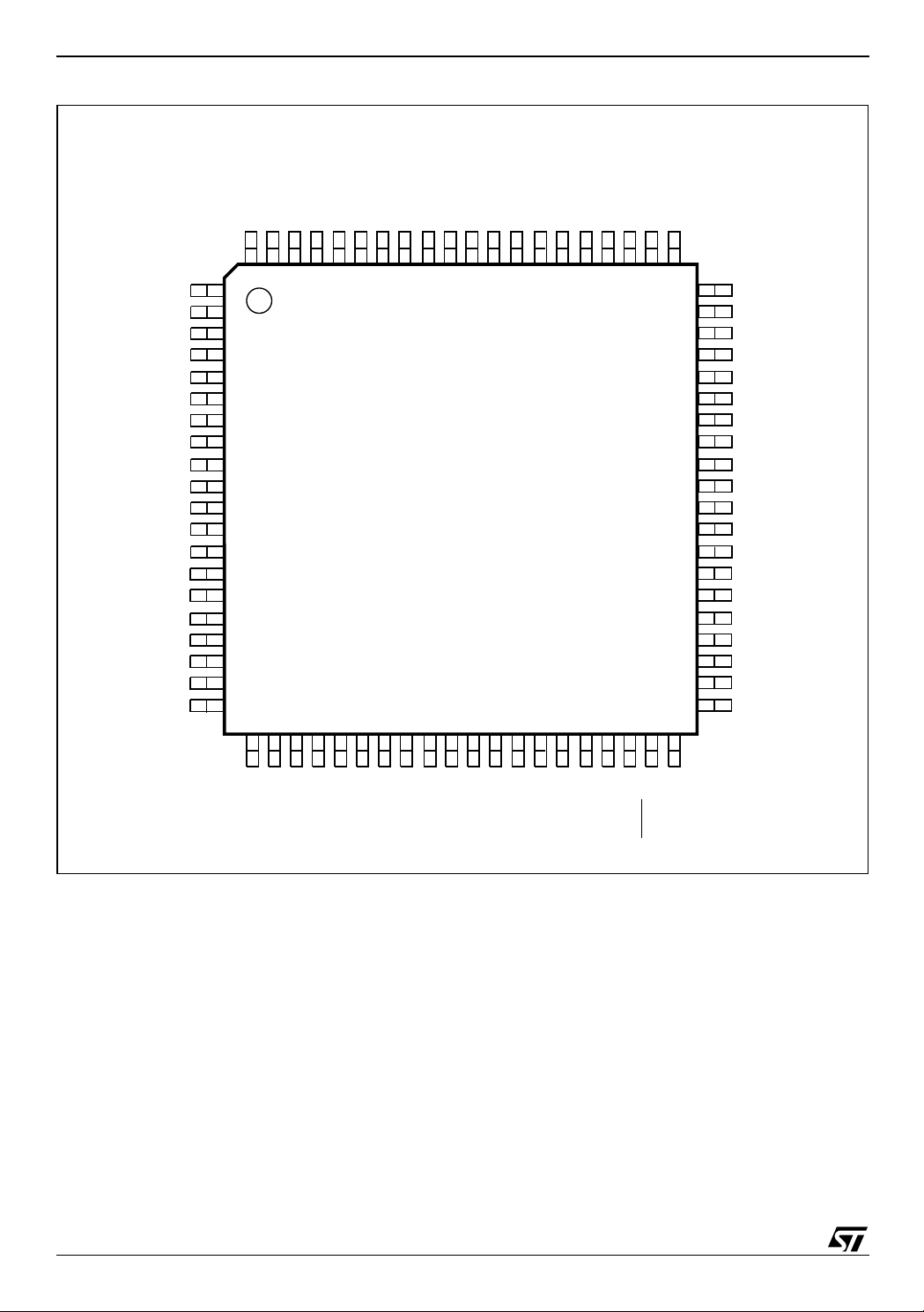
Figure 1. TQFP 80-pin Package
TQFP80 (T)
™
development
www.st.com/psm
™
cable with any PC.
.
Rev. 2.0
1/69March 2003
Page 2

DSM2150F5V
TABLE OF CONTENTS
SUMMARY DESCRIPTION. . . . . . . . . . . . . . . . . . . . . . . . . . . . . . . . . . . . . . . . . . . . . . . . . . . . . . . . . . . 6
Figure 2. System Block Diagram, Two Chip Solution . . . . . . . . . . . . . . . . . . . . . . . . . . . . . . . . . . . . 6
Table 1. DSM2150F5V DSP Memory System Devices. . . . . . . . . . . . . . . . . . . . . . . . . . . . . . . . . . . 7
Table 2. Compatible Analog Devices DSPs . . . . . . . . . . . . . . . . . . . . . . . . . . . . . . . . . . . . . . . . . . . 7
Figure 3. TQFP Connections. . . . . . . . . . . . . . . . . . . . . . . . . . . . . . . . . . . . . . . . . . . . . . . . . . . . . . . 8
ARCHITECTURAL OVERVIEW . . . . . . . . . . . . . . . . . . . . . . . . . . . . . . . . . . . . . . . . . . . . . . . . . . . . . . . 9
DSP Address/Data/Control Interface . . . . . . . . . . . . . . . . . . . . . . . . . . . . . . . . . . . . . . . . . . . . . . . 9
Figure 4. Block Diagram . . . . . . . . . . . . . . . . . . . . . . . . . . . . . . . . . . . . . . . . . . . . . . . . . . . . . . . . . . 9
Main Flash Memory. . . . . . . . . . . . . . . . . . . . . . . . . . . . . . . . . . . . . . . . . . . . . . . . . . . . . . . . . . . . 10
Secondary Flash Memory. . . . . . . . . . . . . . . . . . . . . . . . . . . . . . . . . . . . . . . . . . . . . . . . . . . . . . . 10
Programmable Logic (PLDs) . . . . . . . . . . . . . . . . . . . . . . . . . . . . . . . . . . . . . . . . . . . . . . . . . . . .10
Runtime Control Registers. . . . . . . . . . . . . . . . . . . . . . . . . . . . . . . . . . . . . . . . . . . . . . . . . . . . . . 11
Memory Page Register . . . . . . . . . . . . . . . . . . . . . . . . . . . . . . . . . . . . . . . . . . . . . . . . . . . . . . . . . 11
I/O Ports . . . . . . . . . . . . . . . . . . . . . . . . . . . . . . . . . . . . . . . . . . . . . . . . . . . . . . . . . . . . . . . . . . . . . 11
JTAG ISP Port . . . . . . . . . . . . . . . . . . . . . . . . . . . . . . . . . . . . . . . . . . . . . . . . . . . . . . . . . . . . . . . . 11
Power Management . . . . . . . . . . . . . . . . . . . . . . . . . . . . . . . . . . . . . . . . . . . . . . . . . . . . . . . . . . . . 11
Security and NVM Sector Protection. . . . . . . . . . . . . . . . . . . . . . . . . . . . . . . . . . . . . . . . . . . . . . 11
Pin Assignments . . . . . . . . . . . . . . . . . . . . . . . . . . . . . . . . . . . . . . . . . . . . . . . . . . . . . . . . . . . . . . 11
Table 3. Pin Description (Pin Assignments in Appendix A). . . . . . . . . . . . . . . . . . . . . . . . . . . . . . . 12
RUNTIME CONTROL REGISTER DEFINITION. . . . . . . . . . . . . . . . . . . . . . . . . . . . . . . . . . . . . . . . . . 13
Table 4. CSIOP Registers and Their Offsets (in Hexadecimal). . . . . . . . . . . . . . . . . . . . . . . . . . . .13
DETAILED OPERATION. . . . . . . . . . . . . . . . . . . . . . . . . . . . . . . . . . . . . . . . . . . . . . . . . . . . . . . . . . . . 14
Flash Memories . . . . . . . . . . . . . . . . . . . . . . . . . . . . . . . . . . . . . . . . . . . . . . . . . . . . . . . . . . . . . . . 14
Table 5. Instruction Sequences for 8-bit Operation (Notes 1,2,3,4) . . . . . . . . . . . . . . . . . . . . . . . . 15
Table 6. Instruction Sequences for 16-bit Operation (Notes 1,2,3,4,15) . . . . . . . . . . . . . . . . . . . . . 17
Instruction Sequences . . . . . . . . . . . . . . . . . . . . . . . . . . . . . . . . . . . . . . . . . . . . . . . . . . . . . . . . . 19
Reading Flash Memory. . . . . . . . . . . . . . . . . . . . . . . . . . . . . . . . . . . . . . . . . . . . . . . . . . . . . . . . . 19
Table 7. Status Bit Definition. . . . . . . . . . . . . . . . . . . . . . . . . . . . . . . . . . . . . . . . . . . . . . . . . . . . . . 20
Programming Flash Memory . . . . . . . . . . . . . . . . . . . . . . . . . . . . . . . . . . . . . . . . . . . . . . . . . . . .21
Table 8. 16-Bit Data Bus with BHE . . . . . . . . . . . . . . . . . . . . . . . . . . . . . . . . . . . . . . . . . . . . . . . . . 21
Table 9. 16-Bit Data Bus with WRH and WRL . . . . . . . . . . . . . . . . . . . . . . . . . . . . . . . . . . . . . . . . 21
Figure 5. Data Polling Flowchart . . . . . . . . . . . . . . . . . . . . . . . . . . . . . . . . . . . . . . . . . . . . . . . . . . . 22
2/69
Page 3

DSM2150F5V
PLDs . . . . . . . . . . . . . . . . . . . . . . . . . . . . . . . . . . . . . . . . . . . . . . . . . . . . . . . . . . . . . . . . . . . . . . . . 23
Table 10. DPLD and CPLD Inputs. . . . . . . . . . . . . . . . . . . . . . . . . . . . . . . . . . . . . . . . . . . . . . . . . .23
Figure 6. PLD Diagram . . . . . . . . . . . . . . . . . . . . . . . . . . . . . . . . . . . . . . . . . . . . . . . . . . . . . . . . . . 24
Decode PLD (DPLD) . . . . . . . . . . . . . . . . . . . . . . . . . . . . . . . . . . . . . . . . . . . . . . . . . . . . . . . . . . . 2 5
Figure 7. DPLD Logic Array. . . . . . . . . . . . . . . . . . . . . . . . . . . . . . . . . . . . . . . . . . . . . . . . . . . . . . . 25
Complex PLD (CPLD) . . . . . . . . . . . . . . . . . . . . . . . . . . . . . . . . . . . . . . . . . . . . . . . . . . . . . . . . . . 26
Figure 8. Macrocell and I/O Port . . . . . . . . . . . . . . . . . . . . . . . . . . . . . . . . . . . . . . . . . . . . . . . . . . . 26
Table 11. Output Macrocell Port and Data Bit Assignments . . . . . . . . . . . . . . . . . . . . . . . . . . . . . .27
Figure 9. CPLD Output Macrocell . . . . . . . . . . . . . . . . . . . . . . . . . . . . . . . . . . . . . . . . . . . . . . . . . . 29
Figure 10. Input Macrocell. . . . . . . . . . . . . . . . . . . . . . . . . . . . . . . . . . . . . . . . . . . . . . . . . . . . . . . . 30
DSP Bus Interface . . . . . . . . . . . . . . . . . . . . . . . . . . . . . . . . . . . . . . . . . . . . . . . . . . . . . . . . . . . . . 31
I/O Ports . . . . . . . . . . . . . . . . . . . . . . . . . . . . . . . . . . . . . . . . . . . . . . . . . . . . . . . . . . . . . . . . . . . . . 31
Figure 11. General Port Architecture. . . . . . . . . . . . . . . . . . . . . . . . . . . . . . . . . . . . . . . . . . . . . . . . 32
Port Operating Modes . . . . . . . . . . . . . . . . . . . . . . . . . . . . . . . . . . . . . . . . . . . . . . . . . . . . . . . . . . 32
Table 12. Port Operating Modes . . . . . . . . . . . . . . . . . . . . . . . . . . . . . . . . . . . . . . . . . . . . . . . . . . . 3 3
Ports A, B, and C – Functionality and Structure . . . . . . . . . . . . . . . . . . . . . . . . . . . . . . . . . . . . 34
Figure 12. Port A, B, and C Structure . . . . . . . . . . . . . . . . . . . . . . . . . . . . . . . . . . . . . . . . . . . . . . . 34
Port D – Functionality and Structure. . . . . . . . . . . . . . . . . . . . . . . . . . . . . . . . . . . . . . . . . . . . . . 35
Figure 13. Port D Structure . . . . . . . . . . . . . . . . . . . . . . . . . . . . . . . . . . . . . . . . . . . . . . . . . . . . . . . 35
Port E – Functionality and Structure. . . . . . . . . . . . . . . . . . . . . . . . . . . . . . . . . . . . . . . . . . . . . . 36
Port F – Functionality and Structure . . . . . . . . . . . . . . . . . . . . . . . . . . . . . . . . . . . . . . . . . . . . . . 36
Port G – Functionality and Structure. . . . . . . . . . . . . . . . . . . . . . . . . . . . . . . . . . . . . . . . . . . . . . 36
Figure 14. Port E and G Structure. . . . . . . . . . . . . . . . . . . . . . . . . . . . . . . . . . . . . . . . . . . . . . . . . . 3 6
POWER MANAGEMENT . . . . . . . . . . . . . . . . . . . . . . . . . . . . . . . . . . . . . . . . . . . . . . . . . . . . . . . . . . . 37
POWER-ON RESET, WARM RESET, AND POWER-DOWN . . . . . . . . . . . . . . . . . . . . . . . . . . . . . . . 38
Figure 15. Reset (RESET) Timing. . . . . . . . . . . . . . . . . . . . . . . . . . . . . . . . . . . . . . . . . . . . . . . . . . 38
Table 13. Status During Power-on Reset, Warm Reset and Power-down Mode . . . . . . . . . . . . . . 38
PROGRAMMING IN-CIRCUIT USING JTAG ISP. . . . . . . . . . . . . . . . . . . . . . . . . . . . . . . . . . . . . . . . . 39
Table 14. JTAG Port Signals. . . . . . . . . . . . . . . . . . . . . . . . . . . . . . . . . . . . . . . . . . . . . . . . . . . . . . 39
Initial Delivery State . . . . . . . . . . . . . . . . . . . . . . . . . . . . . . . . . . . . . . . . . . . . . . . . . . . . . . . . . . .40
AC AND DC PARAMETERS. . . . . . . . . . . . . . . . . . . . . . . . . . . . . . . . . . . . . . . . . . . . . . . . . . . . . . . . . 41
Figure 16. PLD ICC /Frequency Consumption (3.3V). . . . . . . . . . . . . . . . . . . . . . . . . . . . . . . . . . .41
MAXIMUM RATING. . . . . . . . . . . . . . . . . . . . . . . . . . . . . . . . . . . . . . . . . . . . . . . . . . . . . . . . . . . . . . . . 42
Table 15. Absolute Maximum Ratings . . . . . . . . . . . . . . . . . . . . . . . . . . . . . . . . . . . . . . . . . . . . . . . 42
3/69
Page 4

DSM2150F5V
DC AND AC OPERATING AND MEASUREMENT CONDITIONS. . . . . . . . . . . . . . . . . . . . . . . . . . . . 43
Table 16. Operating Conditions . . . . . . . . . . . . . . . . . . . . . . . . . . . . . . . . . . . . . . . . . . . . . . . . . . . . 43
Table 17. AC Measurement Conditions. . . . . . . . . . . . . . . . . . . . . . . . . . . . . . . . . . . . . . . . . . . . . . 43
Figure 17. AC Measurement I/O Waveform . . . . . . . . . . . . . . . . . . . . . . . . . . . . . . . . . . . . . . . . . .43
Figure 18. AC Measurement Load Circuit. . . . . . . . . . . . . . . . . . . . . . . . . . . . . . . . . . . . . . . . . . . . 43
Table 18. Capacitance. . . . . . . . . . . . . . . . . . . . . . . . . . . . . . . . . . . . . . . . . . . . . . . . . . . . . . . . . . . 43
Figure 19. Switching Waveforms – Key. . . . . . . . . . . . . . . . . . . . . . . . . . . . . . . . . . . . . . . . . . . . . .44
Table 19. AC Symbols for PLD Timing . . . . . . . . . . . . . . . . . . . . . . . . . . . . . . . . . . . . . . . . . . . . . .44
Table 20. DC Characteristics. . . . . . . . . . . . . . . . . . . . . . . . . . . . . . . . . . . . . . . . . . . . . . . . . . . . . . 45
Table 21. CPLD Combinatorial Timing . . . . . . . . . . . . . . . . . . . . . . . . . . . . . . . . . . . . . . . . . . . . . .46
Table 22. CPLD MicroCell Synchronous Clock Mode Timing . . . . . . . . . . . . . . . . . . . . . . . . . . . . . 46
Table 23. CPLD MicroCell Asynchronous Clock Mode Timing . . . . . . . . . . . . . . . . . . . . . . . . . . . . 47
Figure 20. Input to Output Disable / Enable . . . . . . . . . . . . . . . . . . . . . . . . . . . . . . . . . . . . . . . . . . 47
Figure 21. Asynchronous Reset / Preset. . . . . . . . . . . . . . . . . . . . . . . . . . . . . . . . . . . . . . . . . . . . . 47
Figure 22. Synchronous Clock Mode Timing – PLD . . . . . . . . . . . . . . . . . . . . . . . . . . . . . . . . . . . . 48
Figure 23. Asynchronous Clock Mode Timing (Product Term Clock) . . . . . . . . . . . . . . . . . . . . . . . 48
Figure 24. Input MicroCell Timing (Product Term Clock) . . . . . . . . . . . . . . . . . . . . . . . . . . . . . . . . 49
Table 24. Input MicroCell Timing. . . . . . . . . . . . . . . . . . . . . . . . . . . . . . . . . . . . . . . . . . . . . . . . . . . 4 9
Figure 25. READ Timing . . . . . . . . . . . . . . . . . . . . . . . . . . . . . . . . . . . . . . . . . . . . . . . . . . . . . . . . . 50
Table 25. READ Timing. . . . . . . . . . . . . . . . . . . . . . . . . . . . . . . . . . . . . . . . . . . . . . . . . . . . . . . . . . 50
Figure 26. WRITE Timing . . . . . . . . . . . . . . . . . . . . . . . . . . . . . . . . . . . . . . . . . . . . . . . . . . . . . . . . 51
Table 26. WRITE Timing. . . . . . . . . . . . . . . . . . . . . . . . . . . . . . . . . . . . . . . . . . . . . . . . . . . . . . . . . 5 1
Table 27. Flash Memory Program, WRITE and Erase Times . . . . . . . . . . . . . . . . . . . . . . . . . . . . . 52
Figure 27. Reset (RESET) Timing. . . . . . . . . . . . . . . . . . . . . . . . . . . . . . . . . . . . . . . . . . . . . . . . . . 52
Table 28. Reset (RESET) Timing . . . . . . . . . . . . . . . . . . . . . . . . . . . . . . . . . . . . . . . . . . . . . . . . . . 52
Figure 28. ISC Timing . . . . . . . . . . . . . . . . . . . . . . . . . . . . . . . . . . . . . . . . . . . . . . . . . . . . . . . . . . . 53
Table 29. ISC Timing. . . . . . . . . . . . . . . . . . . . . . . . . . . . . . . . . . . . . . . . . . . . . . . . . . . . . . . . . . . . 53
PACKAGE MECHANICAL . . . . . . . . . . . . . . . . . . . . . . . . . . . . . . . . . . . . . . . . . . . . . . . . . . . . . . . . . . 54
PART NUMBERING . . . . . . . . . . . . . . . . . . . . . . . . . . . . . . . . . . . . . . . . . . . . . . . . . . . . . . . . . . . . . . . 56
APPENDIX A. TQFP80 PIN ASSIGNMENTS. . . . . . . . . . . . . . . . . . . . . . . . . . . . . . . . . . . . . . . . . . . . 57
4/69
Page 5

DSM2150F5V
APPENDIX B. CSIOP REGISTER BIT DEFINITIONS . . . . . . . . . . . . . . . . . . . . . . . . . . . . . . . . . . . . . 58
Table 33. Data-In Registers – Ports A, B, C, D, E, G . . . . . . . . . . . . . . . . . . . . . . . . . . . . . . . . . . . 58
Table 34. Data-Out Registers – Ports A, B, C, D, E, G. . . . . . . . . . . . . . . . . . . . . . . . . . . . . . . . . . 58
Table 35. Direction Registers – Ports A, B, C, D, E, G . . . . . . . . . . . . . . . . . . . . . . . . . . . . . . . . . . 58
Table 36. Drive Registers – Ports A, B, E, G. . . . . . . . . . . . . . . . . . . . . . . . . . . . . . . . . . . . . . . . . . 58
Table 37. Drive Registers – Port C . . . . . . . . . . . . . . . . . . . . . . . . . . . . . . . . . . . . . . . . . . . . . . . . . 5 8
Table 38. Enable-Out Registers – Ports A, B, C . . . . . . . . . . . . . . . . . . . . . . . . . . . . . . . . . . . . . . . 58
Table 39. Input Macrocells – Ports A, B, C . . . . . . . . . . . . . . . . . . . . . . . . . . . . . . . . . . . . . . . . . . .58
Table 40. Output Macrocells A Register . . . . . . . . . . . . . . . . . . . . . . . . . . . . . . . . . . . . . . . . . . . . .59
Table 41. Output Macrocells B Register . . . . . . . . . . . . . . . . . . . . . . . . . . . . . . . . . . . . . . . . . . . . .59
Table 42. Mask Macrocells A Register . . . . . . . . . . . . . . . . . . . . . . . . . . . . . . . . . . . . . . . . . . . . . .59
Table 43. Mask Macrocells B Register . . . . . . . . . . . . . . . . . . . . . . . . . . . . . . . . . . . . . . . . . . . . . .59
Table 44. Flash Memory Protection Register . . . . . . . . . . . . . . . . . . . . . . . . . . . . . . . . . . . . . . . . . 59
Table 45. Flash Boot Protection Register . . . . . . . . . . . . . . . . . . . . . . . . . . . . . . . . . . . . . . . . . . . .59
Table 46. JTAG Enable Register . . . . . . . . . . . . . . . . . . . . . . . . . . . . . . . . . . . . . . . . . . . . . . . . . . . 59
Table 47. Page Register . . . . . . . . . . . . . . . . . . . . . . . . . . . . . . . . . . . . . . . . . . . . . . . . . . . . . . . . . 60
Table 48. PMMR0 Register. . . . . . . . . . . . . . . . . . . . . . . . . . . . . . . . . . . . . . . . . . . . . . . . . . . . . . . 6 0
Table 49. PMMR2 Register. . . . . . . . . . . . . . . . . . . . . . . . . . . . . . . . . . . . . . . . . . . . . . . . . . . . . . . 6 0
Table 50. Memory_ID0 Register . . . . . . . . . . . . . . . . . . . . . . . . . . . . . . . . . . . . . . . . . . . . . . . . . . . 60
Table 51. Memory_ID1 Register . . . . . . . . . . . . . . . . . . . . . . . . . . . . . . . . . . . . . . . . . . . . . . . . . . . 60
APPENDIX C. TYPICAL CONNECTIONS, DSM2150F5V AND ADSP-21535 BLACKFIN DSP. . . . . 61
Figure 30. Typical Connections, DSM2150F5V and ADSP-21535 Blackfin DSP . . . . . . . . . . . . . . 61
Typical Memory Map, DSM2150F5V and ADSP21535 BL ACKFIN DSP. . . . . . . . . . . . . . . . . . . 62
Figure 31. Memory Map, ADSP-21535 . . . . . . . . . . . . . . . . . . . . . . . . . . . . . . . . . . . . . . . . . . . . . . 62
Specifying the Memory Map with PSDsoft Express™. . . . . . . . . . . . . . . . . . . . . . . . . . . . . . . . 63
Table 52. HDL Statements Generated from PSDsoft Express to Implement Memory Map . . . . . . 63
Figure 32. PSDsoft Express™ Memory Mapping . . . . . . . . . . . . . . . . . . . . . . . . . . . . . . . . . . . . . . 63
APPENDIX D. TYPICAL CONNECTIONS, DSM2150F5V AND ADSP-21062 SHARC DSP . . . . . . . 64
Figure 33. Typical Connections, DSM2150F5V and ADSP-21062 Sharc DSP. . . . . . . . . . . . . . . . 64
APPENDIX E. TYPICAL CONNECTIONS, DSM2150F5V AND ADSP-TS101S TIGERSHARC DSP. 65
Figu r e 3 4 . Typical C o n nectio ns, ADSP-TS101 S TigerSHAR C DS P . . . . . . . . . . . . . . . . . . . . . . . . 65
APPENDIX F. TYPICAL CONNECTIONS, DSM2150F5V AND ADSP-2191. . . . . . . . . . . . . . . . . . . . 66
Figure 35. Typical Connections, DSM2150F5V and ADSP-2191M . . . . . . . . . . . . . . . . . . . . . . . . 66
APPENDIX G. TYPICAL CONNECTIONS, DSM2150F5V AND ADSP-2188M . . . . . . . . . . . . . . . . . . 67
Figure 36. Typical Connections, DSM2150F5V and ADSP-2188M . . . . . . . . . . . . . . . . . . . . . . . . 67
REVISION HISTORY . . . . . . . . . . . . . . . . . . . . . . . . . . . . . . . . . . . . . . . . . . . . . . . . . . . . . . . . . . . . . . . 68
5/69
Page 6

DSM2150F5V
SUMMARY DESCRIPTION
The DSM2150F5V is an 8 or 16-bit system memory device for use with the Analog Devices DSPs.
DSM means Digital signal processor System
Memory. A DSM device brings In-System Programmable (ISP) Flash memory, param eter storage, programmable logic, and additional I/O to
DSP systems. The result is a flexible two-chip solution for DSP designs. On-chip integrated memory decode logic makes it easy to map dual banks
of Flash memory to the DSP s in a vari ety of ways
for bootloading or bypassing DSP boot ROM, code
execution, data recording, code swapping, and
parameter storage.
JTAG ISP reduces development time, simplifies
manufacturing flow, and lowers the cost of field upgrades. The JTAG ISP interface eliminates the
need for sockets and pre-programmed memory
and logic devices. End products may be manufactured with a blank DSM device soldered down and
programmed at the end of the assembly line in 15
to 35 seconds with no involvement of the DSP.
Rapidly program test code, then application code
as determined by Just-In Time inventory requirements. Additionally, JTAG ISP reduce s development time by turning fast iterations of DSP code in
the lab. Code updates in the field require no product disassembly. The FlashLINK
ming cable costs $59 USD and plugs into any PC
parallel port. Programming through conventional
device insertion programmers is also available using PSDpro from STMicroelectronics and other 3rd
party programmers. See
www.st.com/psm
™
JTAG program-
.
DSM devices add programmable logic (PLD) and
up to 32 configurable I/O pins to the DSP system.
The state of I/O pins can be driven by DSP software or PLD logic. PLD and I/O conf iguration are
programmable by JTAG ISP. The PLD consists of
more than 3000 gates and has 16 macro cell registers. Common uses for the PLD include chip-selects for external devices, state-machines, simple
shiftier and counters, keypad and control panel interfaces, clock dividers, handshake delay, muxes,
etc., eliminating the need for small external PLDs
and logic devices. Configuration of PLD, I/O, and
Flash memory mapping is easily entered in a
point-and-click environment using the software
development tool, PSDsoft Express
no charge from
www.st.com/psm
™
, available at
. The two-chip
DSP/DSM combination is ideal for systems having
limitations on size, EMI levels, and power consumption. DSM memory and logic are “zero-power”, meaning they automatically go to standby
between memory accesses or logic input changes, producing low active and standby current consumption, which is ideal for battery powered
products.
A programmable security bit in the DSM protects
its contents from unauthorized viewing and copying. When set, the security bit will block access of
programming devices (JTAG or others) to the
DSM Flash memories and PLD configuration. The
only way to defeat the security bit is to erase the
entire DSM device, after which the device is blank
and may be used again. The DSP will always have
access to Flash memory contents through the data
bus, even with security bit set.
Figure 2. System Block Diagram, Two Chip Solution
DSM2150F5V
DSP SYSTEM MEMORY
I/O FLAGS
SERIAL
DEVICE
SERIAL
DEVICE
SDRAM
HOST
MCU
6/69
ANALOG
DEVICES
DSP
ADSP-218x
ADSP-219x
ADSP-2153x
ADSP-2106x
ADSP-2116x
ADSP-TS101S
JTAG DEBUG (All But ADSP-218x Family)
ADDRESS
CONTROL
8 or 16 DATA
FLASH MEMORY
LOGIC
FLASH MEMORY
ADDR& DECODE
16 MACROCELL PLD
I/O CONTROL
POWER MANAGEMENT
CONTENT SECURITY
PRIMARY
512 Kbytes
SECONDARY
32 Kbytes
I/O BUS
16 I/O
PORTS
I/O, PLD, CHIP SELECTS
WITH
PLD
8 to 16
I/O
GENERAL PURPOSE I/O
PORTS
JTAG
ISP TO
ALL
AREAS
JTAG ISP
AI05732
Page 7

Table 1. DSM2150F5V DSP Memory System Devices
Part Number
Main Flash
Memory
Secondary
Flash Mem
PLD
I/O
Ports
V
CC
and I/O
Mem
Speed
DSM2150F5V
Package Op Temp
DSM2150F5V-12T6
512 KBytes,
eight 64-KByte
sectors
32 KBytes,
four 8-KByte
sectors
16
macro
cells
Up to
40
3.3V ±10% 120ns
80-pin
TQFP
Table 2. Compatible Analog Devices DSPs
DSP Part Number Core Operating Voltage I/O Voltage
ADSP-2183, 2184L, 2185L, 2186L, 2187L 3.3V 3.3V
ADSP-2185M, 2186M, 2188M, 2189M 2.5V 3.3V
ADSP-2184N, 2185N, 2186N, 2187N, 2188N, 2189N 1.8V 3.3V
ADSP-2191M, 2195M, 2196M 2.5V 3.3V
Blackfin ADSP-215 32S 3.3V 3.3V
Blackfin ADSP-215 35P 1.5V 3.3V
Sharc ADSP-21060L, 21061L, 21062L, 21065L 3.3V 3.3V
Sharc ADSP-21160M 2.5V 3.3V
Sharc ADSP-21160N, 21161N 1.8V 3.3V
Tiger Sharc ADSP-TS101S 1.0V 3.3V
–40
+85
o
C to
o
C
7/69
Page 8
DSM2150F5V
Figure 3. TQ FP Connection s
PD1
PD0
80797877767574737271706968676665646362
PE7
PE6
PE5
PE4
PE3
PE2
PE1
PE0
GND
VCCPB7
PB6
PB5
PB4
PB3
PB2
PB1
PB0
61
PD2
PD3
AD0
AD1
AD2
AD3
AD4
GND
V
CC
AD5
AD6
AD7
AD8
AD9
AD10
AD11
AD12
AD13
AD14
AD15
1
2
3
4
5
6
7
8
9
10
11
12
13
14
15
16
17
18
19
20
21222324252627282930313233343536373839
CC
PF0
PF1
PF2
PF3
PF4
PF5
PF6
PG0
PG1
PG2
PG3
PG4
PG5
PG6
PG7
V
GND
PF7
RESET
40
CNTL2
60 CNTL1
59 CNTL0
58 PA7
57 PA6
56 PA5
55 PA4
54 PA3
53 PA2
52 PA1
51 PA0
50 GND
49 GND
48 PC7
47 PC6
46 PC5
45 PC4
44 PC3
43 PC2
42 PC1
41 PC0
AI04943
8/69
Page 9

ARCHITECTURAL OVERVIEW
Major functional blocks are shown in Figure 4.
DSP Address/Data/Control Interface
These DSP signals attach directly to the DSM for
a glueless connection. An 8-bit or 16-bit data connection is formed and 16 or more DSP address
lines can be decoded as well as various DSP
memory strobes; i.e.
BMS, RD, AWE, IOMS, MSx,
etc. The data path width must be specified as 8bits or 16-bits in PSDsoft Express. This configura-
Figure 4. Block Diagram
DSM2150F5V
tion is a static, meaning the data path width cannot
switch between 8-bits and 16-bits during runtime.
Port F is used for 8-bit data path, Ports F and G are
used for 16-bit data path. There are many different
ways the DSM2150F5V can be configured and
used depending on system requirements. See Appendices for example connections between the
DSM2150F5V and different DSPs.
DSP ADDR
AD0
AD1
AD2
AD3
AD4
AD5
AD6
AD7
AD8
AD9
AD10
AD11
AD12
AD13
AD14
AD15
DSP DATA
PF0
PF1
PF2
PF3
PF4
PF5
PF6
PF7
DSP DATA
or GP I/O
PG0
PG1
PG2
PG3
PG4
PG5
PG6
PG7
DSP CNTL
CNTL0
CNTL1
CNTL2
RST\
INTERNAL ADDR, DATA, CONTROL BUS LINKED TO DSP
SECURITY
LOCK
PAGE REG
DECODE
PLD
GENERAL PLD
PLD INPUT BUS
PIN FEEDBACK
NODE FEEDBACK
INTERNAL ADDR, DATA, CONTROL BUS LINKED TO DSP
AND
ARRAY
AAAAAAAA
BBBBBBBBCCCCCCCC
FS0-7
CSBOOT0-3
CSIOP
ECS0-7
AAAAAA
AA
BBBBBBBB
16 OUTPUT MICROCELLS
24 INPUT
MICROCELLS
DSM2150F5V
DSP System Memory
MAIN FLASH
8 BLOCKS, 64 KB
512 KBytes total
SECONDARY FLASH
4 BLOCKS, 8 KB
32 KBytes total
RUNTIME CONTROL
GPIO
PLD
POWER MNGMT
JTAG ISP
CONTROLLER
TO PLD
IN BUS
I/O PORT
PD0
PD1
PD2
PD3
I/O PORT
PA0
PA1
PA2
PA3
PA4
PA5
PA6
PA7
I/O PORT
PB0
PB1
PB2
PB3
PB4
PB5
PB6
PB7
I/O PORT
PC0
PC1
PC2
PC3
PC4
PC5
PC6
PC7
I/O PORT
PC0
PC1
PC2
PC3
PC4
PC5
PC6
PC7
AI05776
9/69
Page 10

DSM2150F5V
Main Flash Memory
The 4M bit (512 KByte) Main Flash memory is divided into eight equally-sized 64 KByte sectors
that are individually selectable through the Decode PLD. Each Flash memory s ector can be located at any address as defined by the user with
PSDsoft Express. DSP code and data are easily
placed in flash memory using PSDsoft Express,
the software development tool.
Secondary Flash Memory
The 256Kbit (32 KByte) Secondary Flash memory
is divided into eight equally-sized 8 KByt e sec tors
that are individually selectable through the Decode PLD. Each Flash memory s ector can be located at any address as defined by the user with
PSDsoft Express. DSP code and data can also be
placed Secondary Flash memory using the PSDsoft Express development tool.
Secondary flash memory is good for storing dat a
because of its smaller sectors. Software EEPROM
emulation techniques can be used for small data
sets that change frequently on a byte-by-byte basis.
Secondary flash may also be used to store custom
start-up code for applications that do not “boot” using DMA, but instead start executing code from external memory upon reset (bypass internal DSP
boot ROM). Storing code here can keep the entire
Main Flash free of initialization code for clean software partitioning. If only one or more 8 KByte sectors are needed for start-up code, the remaining
sectors of Secondary Flash may be used for data
storage.
In-Application-Programming (IAP) may be implemented using Secondary Flash. For example,
code to implement IAP over a USB channel may
be stored here. The DSP executes code from Secondary Flash array while erasin g and writing new
code to the Main Flash array as it is received over
the USB channel. Any communication channel
that the DSP supports can be used for IAP.
Secondary Flash may also be used as an extension to Main Flash memory producing a total of
544 KBytes.
Miscellaneous: Main and Secondary Flash memories are totally independent, allowing concurrent
operation. The DSP can read from one memory
while erasing or programming the other. The DSP
can erase Flash memories by individual sectors or
the entire Flash memory array may be erased at
one time. Each sector in either Flas h memory array may be individually write protected, bloc king
any WRITEs from the DSP (good for boot and
start-up code protection). The Flash memories automatically go to standby between DSP READ or
WRITE accesses to conserve power. Maximum
access times include sector decoding time. Maxi-
mum erase cycles is 100K and data retention is 15
years minimum. Flash memory, as well as the entire DSM device may be programmed with the
JTAG ISP interface with no DSP involvement.
Programm a b le Logic (PLDs)
The DSM family contains two PLDS that m ay optionally run in Turbo or Non-Turbo Mode. PLDs operate faster (less propagation delay) while in
Turbo Mode but consume more power than NonTurbo Mode. Non-Turbo Mode allows the PLDs to
automatically go to standby when no inputs are
change to conserve power. The Turbo Mode setting is controlled at runtime by DSP software.
Decode PLD (DPLD). This is programmable logic used to select one of the eigh t individual Main
Flash memory segments, one of four individual
Secondary Flash memory segments, or the group
of control registers within the DSM device. The
DPLD can also drive ex ternal chip select signals
on Port C pins. DPLD input signals include: DSP
address and control signals, Page Register outputs, DSM Port Pins, CPLD logic feedback.
Complex PLD (CPLD). This programmab le logic
is used to c reate bo th combinatorial and sequential general purpose logic. The C PLD contains 16
Output Macrocells (OMCs) and 24 Input Macrocells (IMCs). PSD Macroc ell registers are unique
in that they have direct connection to the DSP data
bus allowing them to be loaded and read directly
by the DSP at runtime. This di rect access is g ood
for making small peripheral devices (shiftier,
counters, state machines, etc.) that are accessed
directly by the DSP with little overhead. DPLD inputs include DSP address and control signals,
Page Register outputs, DSM Port Pins, and CPLD
feedback.
OMCs: The general structure of the CPLD is similar in nature to a 22V10 PLD device wit h t he familiar sum-of-products (AND-OR) construct. True
and compliment versions of 73 input signals are
available to a large AND array. AND array outputs
feed into a multiple product-term O R gate within
each OMC (up to 10 product-terms for each
OMC). Logic output of the OR gate can be passed
on as combinatorial logic or combined with a flipflop within in each OMC to realize sequential logic.
OMCs can be used a s a buried nodes with feedback to the AND array or OMC output can be routed to pins on Port A or Port B.
IMCs: Inputs from pins on Ports A, B or C are routed to IMCs for condi tioning (clocking or latching)
as they enter the chip, which is good for sampl ing
and debouncing inputs. Alternatively, IMCs can
pass Port input signals directly to PLD inputs without clocking or latching. Th e DSP may read the
IMCs at any time.
10/69
Page 11

Runtime Control Registers
A block of 256 byt es is decoded inside the DSM
device for control and status registers. 50 registers
are used from the block of 256 locations to control
the output state of I/O pins, to READ I/O pins, to
control power management, to READ/WRITE
macrocells, and other functions at runtime. See
Table 4 for description. The base address of these
256 locations is referred to in this data sheet as
csiop
(Chip Select I/O Port). Individual registers
within this block are accessed with an offset from
the base address. Some DSPs can ac cess
csiop
registers using I/O memory with the IOMS strobe (if
csiop
equipped).
registers are bytes. When the
DSM is configured for 16-bit operation, csiop registers are read in byte pairs at even addresses
only. Care should be taken while writing
csiop
registers to ensure the proper byte is written within the
byte pair. This is not a problem for DSPs that support the BHE
CNTL2 input pin, or WRL
(Byte High Enable) signal on the
, WRH (WRITE low byte,
WRITE high byte) on the CNTL0 and PD3 input
pins of the DSM2150F5V.
Memory Page Register
This 8-bit register can be l oaded and read b y the
csiop
DSP at runtime as one of the
registers. Its
outputs feed directly into both PLDs. The page
register can be used for special m emo ry mappi ng
requirements and also for general logic.
I/O Po r t s
The DSM has 52 individually configurable I/O pins
distributed over the seven ports (Ports A, B, C, D,
E, F, and G). At least 32 I/O are available when
DSM2150F5V is connected with 8-bit data path,
and at least 24 I/O are available with 16-bit data
path. Each I/O pin can be indiv idually configured
for different functions such as standard MCU I/O
ports or PLD I/O on a pin by pin basis. (MCU I/O
means that for each pin, its output state can be
controlled or its input value can be read by the
csiop
DSP at runtime using the
registers like an
MCU would do.)
The static configuration of all Port pins is d efined
with the PSDsoft Express
™
software development
tool. The dynamic action of the Ports pins is controlled by DSP runtime software.
JTAG ISP Port
In-System Programming (ISP) can be pe rformed
through the JTAG signals on Port E. This serial interface allows programming of the entire DSM device or subsections (that is, only Flash memory, for
example) without the participation of the DSP. A
blank DSM device soldered to a circuit board can
be completely programmed in 15 to 35 seconds.
The basic JTAG signals; TMS, TCK, TDI, and
TDO form the IEEE-1149.1 interface. The DSM
DSM2150F5V
device does not implement the IEEE-1149.1
Boundary Scan functions. The DSM uses the
JTAG interface for ISP only. However, the DSM
device can reside i n a standard JTAG chain with
other JTAG devices and it will remain in BYPASS
Mode while other devices perform Boundary
Scan.
ISP programming time can be reduced as much as
30% by using two more signals on Port E, TSTAT
and TERR
The FlashLINK
available from STMicroelectronics for $USD59
and PSDsoft Express software is available at no
charge from
needed to program a DSM device using the parallel port on any PC or notebook. See sec tion titled
“PROGRAMMING IN-CIRCUIT USING JTAG
ISP” on page 39.
Power Management
The DSM has bits in
figured at run-time by the DSP to reduc e power
consumption of the CPLD. The Turbo Bit in the
PMMR0 register can be set to logic '1' and the
CPLD will go to Non-Turbo Mode, meaning it will
latch its outputs and go to sleep until the next transition on its inputs. There is a slight penalty in PLD
performance (longer propagation delay), but significant power savings are realized.
Additionally, other bits in two
be set by the DSP to selectively block signals from
entering the CPLD which reduces power consumption.
Both Flash memories automatically go to standby
current between accesses. No user action required.
Security and NVM Sector Protection
A programmable security bit in the DSM protects
its contents from unauthorized viewing and copying. When set, the security bit will block access of
programming devices (JTAG or others) to the
DSM Flash memory and PLD configuration. The
only way to defeat the security bit is to erase the
entire DSM device, after which the device is blank
and may be used again.
Additionally, the content s of ea ch in dividual F lash
memory sector can be write protected (sector protection) by configuration with PSDsoft Express
This is typically used to protect DSP boot code
from being corrupted by inadvertent WRITEs to
Flash memory from the DSP.
Pin Assign m ent s
Pin assignment are shown for the 80-pin TQFP
package in Figure 3, page 8, and their description
in Table 3, page 12.
in addition to TMS, TCK, TDI and TDO.
™
JTAG programming cable is
www.st.com/psm
csio p
. That is all that is
registers that are con-
csio p
registers can
™
.
11/69
Page 12
DSM2150F5V
Table 3. Pin Description (Pin Assignments in Appendix A)
Pin Name Type Description
AD0-15 In Sixteen address inputs from the DSP.
CNTL0 In
CNTL1 In Active low READ strobe input from the DSP.
CNTL2 In
Active low WRITE strobe input from the DSP, typically connected to DSP WR
functions as WRL
Programmable control input. CNTL2 may be used for BHE
DSM2150F5V is configured for 16-bit operation. BHE = ’0’ will allow a byte WRITE from data lines
D8-D15 ignoring data lines D0-D7. BHE
lines D8-D15. DSP READ operations are not affected by BHE
for DSPs which use WRL strobe when writing low byte only in 16-bit word.
= 1 will allow a byte WRITE from D0-D7 ignoring data
signal. Also
(Byte High Enable) when
(always read both bytes).
Reset In
PA0-7 I/O
PB0-7 I/O
PC0-7 I/O
PD0-3 I/O
PE0-7 I/O
Active low reset input from system. Resets DSM I/O Ports, Page Register contents, and other
DSM configuration registers. Must be logic Low at Power-up.
Eight configurable Port A signals with the following functions:
1. MCU I/O – DSP may write or read pins directly at runtime with csiop registers.
2. CPLD Output Macrocell (McellA0-7) outputs.
3. Inputs to the PLDs (via Input Macrocells). Can be used to input address A16 and above.
Note: PA0-PA7 may be configured at run-time as standard CMOS or Open Drain Outputs.
Eight configurable Port B signals with the following functions:
1. MCU I/O – DSP may write or read pins directly at runtime with csiop registers.
2. CPLD Output Macrocell (McellB0-7 or McellC0-7) outputs.
3. Inputs to the PLDs (via Input Macrocells). Can be used to input address A16 and above.
Note: PB0-PB7 may be configured at run-time as standard CMOS or Open Drain Outputs.
Eight configurable Port C signals with the following functions:
1. MCU I/O – DSP may write or read pins directly at runtime with csiop registers.
2. DPLD chip-select outputs (ECS0-7, does not consume MicroCells).
3. Inputs to the PLDs (via Input Macrocells). Can be used to input address A16 and above.
Note: PC0-PC7 may be configured at run-time as standard CMOS or Faster Slew Rate Output.
Four configurable Port D signals with the following functions:
1. MCU I/O – DSP may write or read pins directly at runtime with csiop registers.
2. Input to the PLDs (no associated Input Macrocells, routes directly into PLDs). Can be used to
input address A16 and above.
3. PD1 can be configured as CLKIN, a common clock input to PLD.
4. PD2 can be configured as CSI
memory is disabled to conserve more power when CSI
5. PD3 can be used for WRH
Eight configurable Port E signals with the following functions:
1. MCU I/O – DSP may write or read pins directly at runtime with csiop registers.
2. PE0, PE1, PE2, and PE3 can form the JTAG IEEE-1149.1 ISP serial interface as signals TMS,
TCK, TDI, and TDO respectively.
3. PE4 and PE5 can form the enhanced JTAG signals TSTAT and TERR
ISP programming time up to 30% when used in addition to the standard four JTAG signals: TDI,
TDO, TMS, TCK.
4. PE4 can be configured as the Ready/Busy output to indicate Flash memory programming status
during parallel programming. May be polled by DSP or used as DSP interrupt.
Note 1: PE0-PE7 may be configured at run-time as either standard CMOS or Open Drain Outputs.
Note 2: The JTAG ISP pins may be multiplexed with other I/O functions.
, active low Chip Select Input to select Flash memory. Flash
is logic high.
strobe from DSP to write high byte only for 16-bit configuration.
respectively. Reduces
PF0-7 I/O Port F connects to eight data bus signals, D0 - D7 from DSP.
Port G connects to eight data bus signals, D8 - D15 from DSP if 16-bit data path is used.
PG0-7 I/O
V
CC
GND Ground pins
12/69
Otherwise, PG0-PG7 can be used for general purpose MCU I/O pins.
Note: PG0-PG7 may be configured at run-time as standard CMOS or Open Drain Outputs.
Supply Voltage
Page 13

RUNTIME CONTROL REGISTER DEFINITION
A block of 256 addresses are decoded inside the
DSM2150F5V for control and status. 50 locations
contain registers that the DSP a ccesses at runtime. The base address of the registers is called
csio p
(Chip Select I/O Po rt). T able 4 lists the reg-
DSM2150F5V
isters and their offsets (in hex adecimal) from the
csio p
base. See Appendix B for bit definitions.
Note: Do not write to unused locations, they
should remain logic zero.
Note: See Table 13, page 38 for register state at
reset and at power-on.
Table 4.
Data In 00 01 10 11 30 41
Data Out 04 05 14 15 34 45
Direction 06 07 16 17 36 47
Drive Select 08 09 18 19 38 49
Input
Macrocells
Enable Out 0C 0D 1C
Output
Macrocells A
Output
Macrocells B
Mask
Macrocells A
Mask
Macrocells B
Main Flash
Sector Protect
Security Bit
and Secondary
Flash Sector
Protection
JTAG Enable C7
PMMR0 B0 Power Management Register 0. WRITE and READ.
PMMR2 B4 Power Management Register 2. WRITE and READ.
Page E0 Memory Page Register. WRITE and READ.
Memory_ID0 F0 Read to get size of Main Flash memory. No WRITEs.
Memory_ID1 F1 Read to get size of 2nd Flash memory. No WRITEs.
CSIOP
Register
Name
Registers and Their Offsets (in Hexadecimal)
Por
Por
Por
Por
Por
Por
t A
t B
t C
t D
t E
0A 0B 1A Read to obtain state of IMCs. No WRITEs.
20
23
Other Description
t G
MCUI/O Input Mode. Read to obtain current logic
level of Port pins. No WRITEs.
MCU I/O Output Mode. Write to set logic level on
Port pins. Read to check status.
MCU I/O Mode. Configures Port pin as input or
output. Write to set direction of Port pins.
Logic ’1’ = out, Logic ’0’ = in. Read to check status.
Write to configure Port pins as either standard
CMOS or Open Drain on some pins, while selecting
high slew rate on other pins. Read to check status.
Read to obtain the status of the output enable logic
on each I/O Port driver. No WRITEs.
Read to get logic state of output of OMC bank A.
Write to load registers of OMC bank A.
Read to get logic state of output of OMC bank B.
21
Write to load registers of OMC bank B.
Write to set mask for loading OMCs in bank A. Logic
’1’ in a bit position will block READs/WRITEs of the
22
corresponding OMC. Logic ’0’ will pass OMC value.
Read to check status.
Write to set mask for loading OMCs in bank B. Logic
’1’ in a bit position will block READs/WRITEs of the
corresponding OMC. Logic ’0’ will pass OMC value.
Read to check status.
Read to determine Main Flash Sector Protection
C0
Setting. No WRITEs.
Read to determine if DSM devices Security Bit is
active. Logic ’1’ = device secured.
C2
Also read to determine Secondary Flash Protection
Setting status. No WRITEs.
Write to enable JTAG Pins (optional feature). Read
to check status.
13/69
Page 14

DSM2150F5V
DETAILED OPERATION
Figure 4, page 9 s hows major f unctional areas of
the device:
■ Flash Memories
■ PLDs (DPLD, CPLD, Page Register)
■ DSP Bus Interface (Address, Data, Control)
■ I/O Ports
■ Runtime Control Registers
■ JTAG ISP Interface
The following describes these functions in more
detail.
Flash Memories
The Main Flash memory array is divided into eight
equal 64 KByte sectors. The Secondary Flash
memory array is divid ed into four equal 8 K Byte
sectors. Each sector is selected by the DPLD can
be separately protected from program and erase
cycles. This configuration is specified by using PSDsoft Express
Memory Sector Select Signals. The DPLD generates the Select signals for all the internal memory blocks (see Figure 7). Each of the twelve
sectors of the Flash memories has a select signal
FS0-FS7, or CSBOOT0-CSBOOT3
(
tains up to three product terms. Having t hree product terms for each select signal allows a given
sector to be mapped into multiple a re a s o f system
memory if needed.
Ready/Busy
output the Ready/
Busy is a ’0’ (Bus y) when either Flash mem ory ar-
ray is being written,
array is being erased. The ou tput is a ’1’ (Ready)
when no WRITE or Erase cycle is in progress. This
signal may be polled by the DSP or used as a DSP
interrupt to indicate when an erase or program cycle is complete.
™
.
) which con-
(PE4). This signal can be used to
Busy status of the device. Ready/
or
when either Flash me mory
Memory Operation. The Flash memories are ac-
cessed through the DSP Address, Data, and Control Bus Interface.
DSPs and MCUs cannot write to Flash memory as
it would an SRAM device. Flash memory must first
be “unlocked” with a special seq uence of WRITE
operations to invoke an internal algorithm, then a
single data byte (or word if DSM2150F5V is configured for 16-bit operation) is writt en to the Flash
memory array, then programming status is
checked by a READ operation or by checking the
Ready/
Busy pin (PE4). Thi s “unlocking” sequenc e
optionally may be bypassed by using the Unlock
Bypass command to reduce programming time.
Table 5 lists all of the special instruction sequences to program (write) data to the Flash memory arrays, erase the arrays, and check for different
types of status from the arrays when the
DSM2150F5V is configured to operate as an 8-bit
device. Table 6 lists instruction sequences when
the DSM2150F5V is conf igured for 16-bit operation. These instruction sequences are different
combinations of in dividual W RITE an d READ operations.
IMPORTANT: The DSP cannot read and exec ute
code from the same Flash memory array for which
it is directing an instruction sequence. Or more
simply stated, the DSP may not read co de from
the same Flash array that is writing or erasing. Instead, the DSP must execute code from an alternate memory (like its own internal SRAM or a
different Flash array) while sending instructions to
a given Flash array. Since the two Flash memory
arrays inside the DSM device are completely independent, the DSP may read code from one array
while sending instructions to the other.
After a Flash memory array is programmed (written) it will go to “Read Array” Mo de, then th e DSP
can read from Flash memory just as if would from
any ROM or SRAM device.
14/69
Page 15

DSM2150F5V
Table 5. Instruction Sequences for 8-bit Operation (Notes 1,2,3,4)
Instruction
Sequence
Read Memory
Contents
5
Read Flash
Identifier (Main
Flash only)
6,7
Read Memory
Sector Protection
6,7,8
Status
Program a Flash
Byte
Flash Bulk Erase
Flash Sector
10
Erase
Suspend Sector
11
Erase
Resume Sector
12
Erase
Reset Flash
6
Unlock Bypass
Unlock Bypass
Program
13
Unlock Bypass
14
Reset
Note: 1. All values are in hexadec i m al , X = “Don’t care ”
2. A desired i nterna l Flash me mory sect or sele ct signal (F S0 - FS7 or C SBOOT 0 - CSBOOT 3) must be a ctive for each WRIT E or
READ cycle. Only one of these sector select signals will be active at any given time depending on the address presented by the
DSP and the me m ory mapping d ef i ned in PSDsoft Ex press. FS0 - FS 7 and CSBOOT0-CSBOOT3 are active high logic internally.
3. Only add ress Bits A11 -A0 ar e us ed duri ng F lash m emo ry in stru ction sequen ce decod ing bu s cyc les. The indi vidu al se ctor sele ct
signal (FS0 - FS7 or CSBOOT0-CSBOOT3) which is active during the instruction sequences determines the complete address.
4. For WRITE operations, addresses are latched on the falling edge of Write Strobe (WR
of Write Strobe (WR
5. No Unloc k or Instruction cycles are required when the device is i n the Read Array Mode. Operation is like readi ng a ROM device.
6. The Reset Flash instruction is required to return to the normal Read Array Mode if the Error Flag Bit (DQ5) goes High, or after reading the Flash I dentifier or af t er reading the Sector Prote ct i on Status.
Cycle 1 Cycle 2 Cycle 3 Cycle 4 Cycle 5 Cycle 6 Cycle 7
Read byte
from any
valid Flash
memory addr
Write AAh to
XX555h
Write AAh to
XX555h
Write AAh to
XX555h
Write AAh to
9
XX555h
Write AAh to
XX555h
Write 55h
to XXAAAh
Write 55h
to XXAAAh
Write 55h
to XXAAAh
Write 55h
to XXAAAh
Write 55h
to XXAAAh
Write 90h
to XX555h
Write 90h
to XX555h
Write A0h
to XX555h
Write 80h
to XX555h
Write 80h
to XX555h
Read identifier
at addr
XXX01h
Read value at
addr XXX02h
Write
(program)
data to addr
Write AAh to
XX555h
Write AAh to
XX555h
Write 55h
to XXAAAh
Write 55h
to XXAAAh
Write 10h
to XX555h
Write 30h
to another
Sector
Write B0h to
addr in FS0-7
or
CSBOOT0-3
Write 30h to
addr in FS0-7
or
CSBOOT0-3
Write F0h to
addr in FS0-7
or
CSBOOT0-3
Write AAh to
XX555h
Write A0h to
addr in FS0-7
or
CSBOOT0-3
Write 90h to
addr in FS0-7
or
CSBOOT0-3
, CNTL0)
Write 55h
to XXAAAh
Write
(program)
data to
addr
Write 00h
to addr in
FS0-7 or
CSBOOT03
Write 20h
to XX555h
, CNTL0), Data is latched on the rising edge
Write 30h
to another
Sector
15/69
Page 16

DSM2150F5V
7. The DSP cannot invoke this instruction sequence while executing code from the same Flash memory as that for which the instruction sequence is intended. The DSP must fetch, for example, the code from the DSP SRAM when reading the Flash memory Identifier or Sector Protection Status.
8. The data is 00h for an unprotected sector, and 01h for a protected sector. In the fourth cycle, the Sector Select is active, and (A1,A0)
= (1,0)
9. Direct ing this c omma nd to any i n divi dual act ive Fla sh me mory seg men t (F S0 - FS7) w ill i nvok e the bulk era se of all ei ght Flas h
memory sectors. Likewise, directing command to any Secondary Flash sector (CSBOOT0-3) will invoke erase of all four sectors.
10. DSP wr ites c omma nd seque nc e to in itia l se gmen t to be e rase d, th en wr ite s the byte 30 h to a dditi onal sec tors to be era sed. 30h
must be addr essed to one of the ot her Flash memory segments (FS0-7 or CSBO OT 0-3) for each additional segm ent (write 30h t o
any addre ss w ithi n a des ire d s ecto r). N o mo re ti me th an t
mands.
11. The syste m may per form REA D and Prog ram cycl es in non-e ras ing sectors , read the Flas h ID or re ad the Se cto r Prot ect Sta tus,
when in the Suspend Sector Erase Mode. The Suspend Sector Erase instruction sequence is valid only during a Sector Erase cycle.
12. The Resume Sector Erase instruction sequence is valid only during the Suspend Sector Erase Mode.
13. The Unlock Bypass in st ructions requi red prior to the Unlock Bypas s Program Inst ruction.
14. The Unlock Bypass Reset Flash instruction is required to return to reading memory data when the device is in Unlock Bypass Mode.
can elap se be twee n s ubseq uen t add itio nal s ect or era se com-
TIMEOUT
16/69
Page 17

DSM2150F5V
Table 6. Instruction Sequences for 16-bit Operation (Notes 1,2 ,3,4,15)
Instruction
Sequence
Read Memory
Contents
5
Read Flash
Identifier (Main
Flash only)
6,7
Read Sector
Protect Status
6,7,8
Program a Flash
word
Flash Bulk Erase
Flash Sector
10
Erase
Suspend Sector
11
Erase
Resume Sector
12
Erase
Reset Flash
6
Unlock Bypass
Unlock Bypass
Program
13
Unlock Bypass
14
Reset
Note: 1. All values are in hexadec i m al , X = “Don’t care ”
2. A desired i nterna l Flash me mory sect or sele ct signal (F S0 - FS7 or C SBOOT 0 - CSBOOT 3) must be a ctive for each WRIT E or
READ cycle. Only one of these sector select signals will be active at any given time depending on the address presented by the
DSP and the me m ory mapping d ef i ned in PSDsoft Ex press. FS0 - FS 7 and CSBOOT0-CSBOOT3 are active high logic internally.
3. Only add ress Bits A11 -A0 ar e us ed duri ng F lash m emo ry in stru ction sequen ce decod ing bu s cyc les. The indi vidu al se ctor sele ct
signal (FS0 - FS7 or CSBOOT0-CSBOOT3) which is active during the instruction sequences determines the complete address.
4. For WRITE operations, addresses are latched on the falling edge of Write Strobe (WR
of Write Strobe (WR
5. No Unloc k or Instruction cycles are required when the device is i n the Read Array Mode. Operation is like readi ng a ROM device.
6. The Reset Flash instruction is required to return to the normal Read Array Mode if the Error Flag Bit (DQ5) goes High, or after reading the Flash I dentifier or af t er reading the Sector Prote ct i on Status.
Cycle 1 Cycle 2 Cycle 3 Cycle 4 Cycle 5 Cycle 6 Cycle 7
Read word
from even addr
Write XXAAh
to XXAAAh
Write XXAAh
to XXAAAh
Write XXAAh
to XXAAAh
Write XXAAh
9
to XXAAAh
Write XXAAh
to XXAAAh
Write XX55h
to XX554h
Write XX55h
to XX554h
Write XX55h
to XX554h
Write XX55h
to XX554h
Write XX55h
to XX554h
Write
XX90h to
XXAAAh
Write
XX90h to
XXAAAh
Write
XXA0h to
XXAAAh
Write
XX80h to
XXAAAh
Write
XX80h to
XXAAAh
Read
identifier at
addr
XXX02h
Read value
at addr
XXX04h
Write word
to even
address
Write
XXAAh to
XXAAAh
Write
XXAAh to
XXAAAh
Write
XX55h to
XX554h
Write
XX55h to
XX554h
Write
XX10h to
XXAAAh
Write
XX30h to
new Sector
Write XXB0h
to even addr in
FS0-7 or
CSBOOT0-3
Write XX30h to
even addr in
FS0-7 or
CSBOOT0-3
Write XXF0h to
even addr in
FS0-7 or
CSBOOT0-3
Write XXAAh
to XXAAAh
Write XX55h
to XX554h
Write
XX20h to
XXAAAh
Write XXA0h
to even addr in
FS0-7 or
Write word to
even addr
CSBOOT0-3
Write XX90h to
even addr in
FS0-7 or
CSBOOT0-3
, CNTL0)
Write XX00h
to even addr
in FS0-7 or
CSBOOT0-3
, CNTL0), Data is latched on the rising edge
Write
to
XX30h
new Sector
17/69
Page 18

DSM2150F5V
7. The DSP cannot invoke this instruction sequence while executing code from the same Flash memory as that for which the instruction sequence is intended. The DSP must fetch, for example, the code from the DSP SRAM when reading the Flash memory Identifier or Sector Protection Status.
8. The data is XX00h for an unprotected sector, and XX01h for a protected sector. In the fourth cycle, the Sector Select is active, and
(A1,A0) = (1,0)
9. Direct ing this c omma nd to any i n divi dual act ive Fla sh me mory seg men t (F S0 - FS7) w ill i nvok e the bulk era se of all ei ght Flas h
memory sectors. Likewise, directing command to any Secondary Flash sector (CSBOOT0-3) will invoke erase of all four sectors.
10. DSP writ es comm and seque nce to ini tial seg ment to be er ased, then w rites the word XX3 0h to addi tional sectors to be erased.
XX30h must be addressed to one of the other Flash memory segments (FS0-7 or CSBOOT0-3) for each additional segment (write
XX30h to any address within a desired sector). No more time than t
commands.
11. The syste m may per form REA D and Prog ram cycl es in non-e ras ing sectors , read the Flas h ID or re ad the Se cto r Prot ect Sta tus,
when in the Suspend Sector Erase Mode. The Suspend Sector Erase instruction sequence is valid only during a Sector Erase cycle.
12. The Resume Sector Erase instruction sequence is valid only during the Suspend Sector Erase Mode.
13. The Unlock Bypass in st ructions requi red prior to the Unlock Bypas s Program Inst ruction.
14. The Unlock Bypass Reset Flash instruction is required to return to reading memory data when the device is in Unlock Bypass Mode.
15. All bus cycles in an instruction sequence are WRITE s or READs to an eve n address (XX AAAh or XX554h ), and only the low byte,
D0-D7, is si gnificant (u pper byte on D8 -D15 is ignored). A Flash mem ory Program bus cycle wri tes a word to an even address.
can elapse between subsequent additional sector erase
TIMEOUT
18/69
Page 19

Instruction Sequences
An instruction sequence consists of a sequence of
specific WRITE or READ operations.
IMPORTANT:
When the DSM2150F5V is configured for 8-bit operations, all instruction sequences consist of byte
WRITE and READ operations on an ev en or odd
address boundary. Flash memory locations are
programmed in bytes to even or odd addresses.
When the DSM2150F5V is configured for 16-bit
operation, all instruction sequences consist of
word WRITE and READ operations on even address boundaries only. The lower byte on D0-7 is
significant and the upper byte on D8-15 is ignored
during instructions and status. Flash memory locations are programmed in 1 6-bit words t o even addresses only.
Each byte/word w ritten to the device is received
and sequentially decoded and not executed as a
standard WRITE operation to the memory array
until the entire command string has been received.
The instruction sequence is executed when the
correct number of bytes/words are properly received and the time between two consecutive
bytes/words is shorter than the time-out period,
t
TIMEOUT
. Some instruction sequences are structured to include READ o perations after the initial
WRITE operations.
The instruction sequence must be followed exac tly. Any invalid combination of instruction bytes/
words or time-out between two consecutive bytes/
words while addressing Flash memory resets the
device logic into Read Array Mode (Flash memory
is read like a ROM device). The device supports
the instruction sequences summarized in Table 5,
page 15 and Table 6, page 17:
Flash memory:
■ Read memory contents
■ Read Main Flash Identifier value
■ Read Sector Protection Status
■ Program a Byte/Word
■ Erase memory by chip or sector
■ Suspend or resume sector erase
■ Reset to Read Array Mode
■ Unlock Bypass Instruction s
For efficient decoding of the instruction sequences, the first two bytes/words of an instruction sequence are the coded cycles and are followed by
an instruction byte/word or confirmation byte/
word. The coded cycles co nsist of writing the d ata
AAh to address XX555h (or XXAAh to address
XXAAAh for 16-b it m ode) dur ing t he fi rst cyc le and
data 55h to address XXAAAh (or XX55h to address XX554 for 16-bit mode) during the second
DSM2150F5V
cycle. Address input signals A12 and a bove are
“Don’t care” during the instruction sequence
WRITE cycles. However, the appropriate internal
Sector Select (
see Table 7, page 2 0) m us t be s elected i nte rnally
(active low is lo gic ’1 ’).
Reading Flash Memory
Under typical conditions, the D SP may read the
Flash memory using READ operations just as it
would a ROM or RAM device. Alternately, the DSP
may use READ operations to obtain sta tus information about a Program or Erase cycle that is currently in progress. Lastly, the DSP may use
instruction sequences to read special data from
these memory blocks. The following sections describe these READ instruction sequences.
Read Memory Contents. Flash memory is
placed in the Read Array Mode after Power-up,
chip reset, or a Reset Flash memory instruction
sequence (see Table 5, page 15 or Tabl e 6, p age
17). The DSP can read the memory contents of
the Flash memory by using READ o perations any
time the READ operation is not part of an instruction sequence. Bytes are read from ev en or odd
addresses when the DSM2150F 5V is configured
for 8-bit operation. Only 16-bit words are read from
even addresses when the DSM2150F5V is configured for 16-bit operations.
Read Main Flash Identifier. The Main Flash
memory identifier is read with an instruction sequence composed of 4 operations: 3 specific
WRITE operations and a READ operation (see Table 5, page 15 or Table 6, page 17). During the
READ operation the appropriate internal Sector
Selec t (
FS0-FS7
E8h (or XXE8h for 16-bit mode). Not applicable to
Secondary Flash.
Read Memory Sector Protection Status. The
Flash memory Sector Protection Status is read
with an instruction sequence composed of 4 operations: 3 specific WRITE ope rations and a READ
operation (see Table 5, page 15 or Table 6, page
17). The READ operation will produce 01h (XX01h
for 16-bit mode) if the Flash sector is prot ect ed or
00h (XX00h or 16-bit mode) if the sector is not protected. Internal Sector Select (FS0-FS7 or
CSBOOT0-CSBOOT3) designates the Flash
memory sector whose protection has to be verified.
Alternatively, the sector protection status can also
be read by the DSP accessing the Flash memory
Protection registers in
tion entitled “Flash Memory Sector Protect” for
register definitions.
FS0-FS7 or CSBOOT0-CSBOOT3
) must be act ive. T he identifier is
csiop
space. See the sec-
,
19/69
Page 20

DSM2150F5V
Table 7. Status Bit Definition
Functional Block
Flash Memory
Note: 1. X = Not guarant eed value, can be read either ’1’ or ’0.’
2. DQ7-DQ0 represent the Data Bus bits, D7-D0.
3. When the DSM2150F5V is configured for 16-bit o peration, DQ8-DQ15 are not si gnificant a nd can be ignored.
FS0-FS7, or
CSBOOT0-CSBOOT3
Active (the desired
segment is selected)
DQ7 DQ6 DQ5 DQ4 DQ3 DQ2 DQ1 DQ0
Data
Polling
Toggle
Flag
Error
Flag
Erase
X
Time-
out
XXX
Reading the Erase/Program Status Bits. The
device provides several status bits to b e used by
the DSP to confirm the completion of an Erase or
Program cycle of Fl ash memory. These stat us bits
minimize the time that the DSP spends performing
these tasks and are defined in Table 7. The status
bits can be read as many times as needed. DQ8 DQ15 are insignificant an d can be ignored when
the DSM2150F5V i s configured to operate in 16bit mode, however, the READ op eration must occur on an even address boundary.
For Flash memory, the DSP can perform a RE AD
operation to obtain these status bits while an
Erase or Program instruction sequence is being
executed by the embedded algorithm. See the
section entitled “Programming Flash Memory”, on
page 21, for details.
Data Polling Flag (DQ7). When erasing or programming in Flash memory, the Data Polling Flag
Bit (DQ7) outputs the complement of the bit being
entered for programming/writing on the Data P olling Flag Bit (DQ7). Once the Progra m instruction
sequence or the W RITE operation is completed,
the true logic value is read on the Data Polling Flag
Bit (DQ7).
– Data Polling is effective after the fourth WRITE
pulse (for a Program instruction sequence) or
after the sixth WRITE pulse (for an Erase
instruction sequence). It must be performed at
the address being programmed or at an address
within the Flash memory sector being erased.
– During an Erase cycle, the Data Polling Flag Bit
(DQ7) outputs a ’0.’ After completion of the
cycle, the Data Polling Flag Bit (DQ7) outputs
the last bit programmed (it is a ’1’ after erasing).
– If the byte/word to be programmed is in a
protected Flash memory sector, the instruction
sequence is ignored.
– If all the Flash memory sectors to be erased are
protected, the Data Polling Flag Bit (DQ7 ) is
reset to ’0’ for t
TIMOUT
, and then returns to the
previous addressed byte. No erasure is
performed.
Toggle Flag ( DQ6 ). The device offers an alternative way for determining whe n the Flash me mory
Program cycle is completed. During the internal
WRITE operation and when the Sector Select
FS0-FS7 (or CSBOOT0-CSBOOT3) is true, the
Toggle Flag Bit (DQ6) toggles from ’0’ to ’1’ and ’1’
to ’0’ on subsequent attem pts to read any byte of
the memory. When the DSM2150F5V is configured to operate in 16-bit mode, status READs
must occur at even addresses, DQ8 - DQ15 are insignificant and can be ignored.
When the internal cycle is complete, the toggling
stops and the data READ on the Data Bus is t he
addressed memory byt e/word. The device is now
accessible for a new RE AD or WRITE operat ion.
The cycle is finished when two successive READs
yield the same output data.
– The Toggle Flag Bit (DQ6) is effective after the
fourth WRITE operation (for a Program
instruction sequence) or after the sixth WRITE
operation (for an Erase instruction sequence).
– If the byte/word to be programmed belongs to a
protected Flash memory sector, the instruction
sequence is ignored.
– If all the Flash memory sectors selected for
erasure are protected, the Toggle Flag Bit
(DQ6) toggles to ’0’ for t
TIMOUT
and then returns
to the previous addressed byte.
Error Flag (DQ5). During a normal Program or
Erase cycle, the Error Flag Bit (DQ 5 ) is to ’ 0. ’ Thi s
bit is set to ’1’ when there is a failure during Flash
memory byte/word Program operation, Sector
Erase, or Bulk Erase operation.
In the case of Flash memory programming, the Error Flag Bit (DQ5) indicates the attempt to program
a Flash memory bit from the programmed state,
logic ’0,’ to the erased state, logic ’1’, which is not
valid. The Error Flag Bit (DQ5) may also indicate a
Time-out condition while attempting to program a
byte/word.
In case of an error in a Flash memory Sector Erase
or byte/word Program cycle, the Flash memory
sector in which the error occurred or to w hich the
programmed byte/word belongs must no longer be
used. Other Flash memory sectors may still be
used. The Error Flag Bit (DQ5) is reset after a Reset Flash instruction sequence.
20/69
Page 21

DSM2150F5V
Erase Time-out Flag (DQ3). The Erase Time-
out Flag Bit (DQ 3) reflects the time-out period allowed between two consecutive Sec tor Erase instruction sequence bytes/words. The Erase Timeout Flag Bit (DQ3) is reset to ’0’ after a Sector
Erase cycle for a time per iod t
TIMOUT
unless an additional Sector Erase instruction sequence is decoded. After this time period, or when the
additional Sector Erase instruction sequence is
decoded, the Erase Time-out Flag Bit (DQ3) is set
to ’1.’
Programming Flash Memory
When the DSM2150F5V is configured for 8-bit operation, Flash memory locations are programmed
in 8-bit bytes to even or odd addresses.
When the DSM2150F5V is configured for 16-bit
operation, Flash memory locations are programmed in 16-bit words to even addresses only.
However, some DSPs support the BHE (byte high
enable) signal on the DSM2150F5V CNTL2 input
or the WRL, WRH (Write Low Byte, Write High
Byte) signals on the CNTL0 and PD3 inputs. In
these cases, a DSP WRITE operation can be directed to an individual byte (upp er or lower) of a
byte-pair. These signals do not effect READ operations, only WRITEs. READs are always by 16bits from an even address.
signal on CNT2 input. See Table 8. Even-
BHE
byte refers to locations with address A0 eq ual to
’0,’ and odd byte as locations with A0 equal to ’1.’
WRL
and WRH signals on CNT0 and PD3 in-
puts. See Tab le 9. Even-byte refers to locations
with address A0 equal to ’0,’ and odd byte as locations with A0 equal to ’1.’
When a byte/word of Flash memory is programmed, individual bits are prog ramm ed to logic
’0.’ You cannot p rogram a bit in F lash mem ory to
a logic ’1’ once it has been programmed to a logic
’0.’ A bit must be erased to logic ’1,' and programmed to logic ’0.’ That means Fla sh memory
must be erased prior to being programme d. The
DSP may erase the entire Flash mem ory array all
at once or individual sector-by-sector, but not byteby-byte (or word-by-word for 16-bit mode). However, the DSP may program Flash memory byte-bybyte (or word-by-word for 16-bit mode).
The Flash memory requires the DSP to send an instruction sequence to program a byte or to erase
sectors (see Table 5 or 6).
Once the DSP issues a Flash memory Program or
Erase instruction sequence, it must check for the
status bits for completion. The embedded algorithms that are invoked inside the device p rovide
several ways give status to the DSP. Status may
be checked using any of three methods: Data Polling, Data Toggle, or Ready/Busy
(pin PE4).
Table 8. 16-Bit Data Bus with BHE
BHE A0 D15-D8 D7-D0
0 0 Odd Byte Even Byte
0 1 Odd Byte —
1 0 — Even Byte
Table 9. 16-Bit Data Bus with WRH and WRL
WRH WRL D15-D8 D7-D0
0 0 Odd Byte Even Byte
0 1 Odd Byte —
1 0 — Even Byte
21/69
Page 22

DSM2150F5V
Data Polling. Polling o n the Da t a Polling Fla g Bit
(DQ7) is a method of checking whether a Program
or Erase cycle is in progress or has completed.
Figure 5 show s the D a t a Polling algor it h m.
When the DSP issues a Program instruction sequence, the embedded algorithm within the device
begins. The DSP then reads the location of the
byte/word to be programmed in Flash memory to
check status. For 16-bit operation, the status location READ must b e at an even addres s and D8D15 can be ignored. The Data Polling Flag Bit
(DQ7) of this location becomes the compli ment of
Bit 7 of the original data byte/word to be programmed. The DSP continues to poll this location,
comparing the Data Polling Flag Bit (DQ7) and
monitoring the Error Flag Bit (DQ5). When the
Data Polling Flag Bit (DQ7) m atches Bit 7 of the
original data, and the Error Flag Bit (DQ5) remains
’0,’ then the embedded algorithm is complete. If
the Error Flag Bit (DQ5) is ’1,’ the DSP should t est
the Data Polling Flag Bit (DQ7) again since the
Data Polling Flag Bit (DQ7) may have changed simultaneously with the Error Flag Bit (DQ 5) (see
Figure 5).
The Error Flag Bit (DQ5) is set if either an internal
time-out occurred while the embedded algorithm
attempted to program t he by te/word or if the DSP
attempted to program a ’1’ to a bit that was not
erased (not erased is logic ’0’).
It is suggested (as with all Flash memories) to read
the location again after the embedded programming algorithm has completed, to compare the
byte/word hat was written to the Flash memory
with the byte/word that was intended to be written.
When using the Data Polling method during an
Erase cycle, Figure 5 still applies. However, the
Data Polling Flag Bit (DQ7) is ’0’ until the Erase cycle is com plete. A ’1’ on the Error Flag B it (DQ5)
indicates a time-out condition on th e Erase cycle,
a ’0’ indicates no error. The DSP can read any location (must be even address for 16-bit mode)
within the sector being erased to get the Data Polling Flag Bit (DQ7) and the Error Flag Bit (DQ5).
PSDsoft Express generates ANSI C code functions which implement these Data Polling algorithms.
Figure 5. Dat a Po ll i ng F lo wc h a rt
START
READ DQ5 & DQ7
at VALID ADDRESS
DQ7
YES
=
DATA
NO
NO
DQ5
= 1
YES
READ DQ7
DQ7
YES
=
DATA
NO
FAIL PASS
AI01369B
22/69
Page 23

PLDs
The PLDs bring programmable logic to the device.
After specifying the logic for the PLDs using PSDsoft Express, the logic is programmed into the device and available upon Power-up.
The PLDs have selectable levels of performance
and power consumption.
The device contains tw o PLDs: the Decode PLD
(DPLD), and the Complex PLD (CPLD), as shown
in Figure 6, page 24.
The DPLD performs address decoding, and generates select signals for internal and external components, such as memory, registers, and I/O ports.
The DPLD can generate e ight External Chip Select (ECS0-ECS7) signals on Port C.
The CPLD can be used for logic functions, such as
loadable counters and shift registers, state machines, and encoding and decoding logic. These
logic functions can be constructed using the 16
Output Macrocells (OMC), 24 Input Macrocells
(IMC), and the AND Array.
The AND Array is used to form product terms.
These product terms are configured from the logic
definition entered in PSDsoft Express. A PLD Input Bus consisting of 73 signals is connected to
the PLDs. Input signals are shown in Table 10.
Turbo Bit. The PLDs in the device can minimize
power consumption by switching to standby when
inputs remain unchanged for an extended time
t
. Resetting the Turbo Bit to ’0’ (Bit 3 of the
TURBO
PMMR0 register) a utomatically places the PLDs
into standby if no inputs are changing. Turning the
Turbo Mode off increases propagation delays
while reducing power consumption. Additionally,
seven bits are available in the P MMR registers in
csio p
to block DSP control signals from entering
DSM2150F5V
the PLDs. This reduces po wer consumption and
can be used only when these DSP control signals
are not used in PLD logi c equations. Each of the
two PLDs has unique characteristics suited for its
applications. They are des cribed in the following
sect ions.
Table 10. DPL D a nd CP LD I nputs
Input Source Input Name
1
DSP Address Bus
DSP Control Signals
Reset RST
PortA Input Macrocells PA7-PA0 8
PortB Input Macrocells PB7-PB0 8
PortC Input Macrocells PC7-PC0 8
Port D Inputs PD3-PD0 4
Page Register PG7-PG0 8
Macrocell A Feedback MCELLA FB7-0 8
Macrocell B Feedback MCELLB FB7-0 8
Flash memory
Program Status Bit
Note: 1. DSP address lines above A15 may enter the DSM device
on any pin on ports A, B, C or D. See Appendices for recommended connections.
2. Additional DSP control signals may enter the DMS device
on any pin on Ports A, B, C, or D. See Appendices for recommended connections.
A15-A0 16
2
CNTL2-CNTL0 3
1
Ready/Busy
1
Number
of
Signals
23/69
Page 24

DSM2150F5V
Figure 6. PLD D iag ram
Data
Bus
PLD INPUT BUS
8
PAGE
REGISTER
73
16
DECODE PLD
(DPLD)
Output Macrocell Feedback
CPLD
73
Direct Macrocell Input to MCU Data Bus
PT
ALLOC.
8
4
1
8
1
16 Output
Macrocell
24 Input Macrocell
(PORT A, B,C)
Main Flash Memory Selects
Secondary Flash Memory Selects
CSIOP Select
External Chip Selects to Port C
JTAG Select
Direct Macrocell Access from MCU Data Bus
I/O PORTS
MCELLA
to PORT A
MCELLB
to PORT B
8
8
24
4
Input Macrocell and Input Ports
PORT D Inputs
AI05769
24/69
Page 25

Decode PLD (DPLD)
The DPLD, shown in Figure 7, is used fo r decoding the address for internal and external com ponents. The DPLD can be used to generate the
following decode signals:
■ 8 Main F lash memo ry S ecto r Se l ect (
FS0-FS7
signals with three product terms each
■ 4 Secondary Flash memory Sector Select
(
CSBOOT0-CSBOOT3
) signals with three
product terms each
Figure 7. DPLD Lo gi c Array
DSM2150F5V
■ 1 internal
and status registers (
of the block of 256 byte locations)
■ 1 JTAG Select signal (enables JTAG operations
)
on Port E when multiplexing JTAG signals with
general I/O signals)
■ 8 external chip select output signals for Port C
pins, each with one product term.
csiop
sele c t for DS M devi ce cont r o l
csiop
is the base address
I/O PORTS (PORT A,B,C)
MCELLA.FB [ 7:0] (Feedback)
MCELLB.FB [ 7:0] (Feedback)
PG0-PG7
A[15:0]
PD[3:0]
CNTRL[2:0] (Read/Write Control Signals)
RESET
RD_BSY
(INPUTS)
(24)
(8)
(8)
(8)
(16)
(4)
(3)
(1)
(1)
3
3
3
3
3
3
3
3
3
3
3
3
1
1
1
CSIOP
JTAGSEL
ECS0
CSBOOT0
CSBOOT1
CSBOOT2
CSBOOT3
FS0
FS1
FS2
FS3
FS4
FS5
FS6
FS7
I/O Decoder
Select
JTAG ISP
4 Secondary
Flash Memory
Sector Selects
8 Flash Main
Memory
Sector Selects
1
1
1
1
1
1
1
ECS1
ECS2
ECS3
ECS4
ECS5
ECS6
ECS7
External Chip Selects
to PORT C
AI05775
25/69
Page 26

DSM2150F5V
Complex PLD (CPLD)
The CPLD can be used to implement system logic
functions, such as loadable counters and shift registers, system mailboxes, ha ndshaking protocols,
state machines, and random logic. See Application Note
AN1171
ic using PSDsoft Express.
The CPLD has the following blocks:
■ 24 Input Macrocells (IMC)
■ 16 Output Macrocells (OMC)
■ Product Term Allocator
■ AND Array capable of generating up to 190
product terms
■ Two I/O Ports.
Figure 8. Ma crocell and I/O Por t
for details on how to s pecify log-
Product Terms
from other
MacrocellS
DSP ADDRESS / DATA BUS
Each of the blocks are described in the sections
that fo llow.
The IMCs and OMCs are connected to the device
internal data bus and can be directly acces sed by
the DSP. This enables the DSP software to load
data into the OMC or read data from both the IMCs
and OMCs. This feature allows efficient implementation of system logic and eliminates the need to
connect the data bus to the AND Array as required
in most standard PLD macro cell architectures.
PLD INPUT BUSPLD INPUT BUS
AND ARRAY
CPLD Macrocells
PRODUCT TERM
ALLOCATOR
UP TO 10
PRODUCT TERMS
POLARITY
SELECT
PT
CLOCK
GLOBAL
CLOCK
CLOCK
SELECT
PT CLEAR
PT INPUT LATCH GATE/CLOCK
PT PRESET
MUX
PT Output Enable (OE
Macrocell Feedback
I/O Port Input
MCU DATA IN
PR DI LD
D/T
D/T/JK FF
SELECT
CK
CL
)
MCU LOAD
Q
COMB.
/REG
SELECT
MUX
DATA
LOAD
CONTROL
Macrocell
Out to
MCU
I/O PORTS
DATA
D
Q
WR
CPLD OUTPUT
PDR
INPUT
Q
D
DIR
REG.
WR
Input Macrocells
MUX
MUX
Q
D
QD
G
I/O Pin
AI05770
26/69
Page 27

DSM2150F5V
Output Macrocell (OMC). Eight of the OMCs,
McellA0-McellA7, are connected to Port A pins.
The other eight Macrocells, Mc ellB0-McellB7, are
connected to Ports B pins. OMCs may be used for
internal feedback (buried registers), or their outputs may be routed to external Port pins.
The OMC architecture is shown in Figure 9. As
shown in the figure, there are native product terms
available from the AND Array, and borrowed product terms available (if unused) from other OMC.
The polarity of the product term is controlled by the
XOR gate. The OMC can implement either sequential logic, using the flip-flop elem ent, or com-
binatorial logic. The multiplexer selects between
the sequential or combinatorial logic outputs. T he
multiplexer output can d rive a port pi n and has a
feedback path to the AND Array inputs.
The flip-flop in the OMC block can be configured
as a D, T, JK, or SR type in PSDsoft Express
The flip-flop’s clock, preset, and clear inputs may
be driven from a product term of the AND A rray.
Alternatively, CLKIN (PD1) can be used for the
clock input to the flip-flop. The f lip-flop is clocked
on the rising edge of CLKIN (PD1). The preset and
clear are active High inputs. Each clear input can
use up to two product terms.
Table 11. Output Macrocell Port and Data Bit Assignments
Output
Macrocell
McellA0 Port A0 3 6 D0 D0
McellA1 Port A1 3 6 D1 D1
McellA2 Port A2 3 6 D2 D2
McellA3 Port A3 3 6 D3 D3
McellA4 Port A4 3 6 D4 D4
McellA5 Port A5 3 6 D5 D5
Port
Assignment
Native Product
T erms
Maximum
Borrowed
Product Terms
Data Bit for
Loading or
Reading in 16-bit
Mode
Data Bit for
Loading or
Reading in 8-bit
Mode
™
.
McellA6 Port A6 3 6 D6 D6
McellA7 Port A7 3 6 D7 D7
McellB0 Port B0 4 5 D8 D0
McellB1 Port B1 4 5 D9 D1
McellB2 Port B2 4 5 D10 D2
McellB3 Port B3 4 5 D11 D3
McellB4 Port B4 4 6 D12 D4
McellB5 Port B5 4 6 D13 D5
McellB6 Port B6 4 6 D14 D6
McellB7 Port B7 4 6 D15 D7
27/69
Page 28

DSM2150F5V
Product Term Al lo c at or. The CPLD has a Prod-
uct Term Allocator. PSDsoft Express
™
uses the
Product Term Allocator to borrow and plac e product terms from one Macrocell to another. This happens automatically in PSDsoft Express
™
, but
understanding how allocation works will help you if
your logic design does not “f it”, in which c ase y ou
may try selecting a different pin or different OM C
where the allocation resources m ay di ffer and the
design will then fit. The fo llowing list summarizes
how product terms are allocated:
■ McellA0-McellA7 all have three native product
terms and may borrow up to six more
■ McellB0-McellB3 all have four native product
terms and may borrow up to five more
■ McellB4-McellB7 all have four native product
terms and may borrow up to six more.
Each Macrocell may only borrow product terms
from certain other Macrocells. Product terms already in use by one Macrocell are not available for
another Macrocell. Product term allocation does
not add any propagation delay to the logic.
If an equation requires more product terms than
are available to it through product term allocation,
then “external” product terms are required, which
consumes other OMC. This is called product term
expansion and also happens automatically in PSDsoft Express
™
as needed. Product tern expansion causes additional propagation delay because
an OMC is consumed by the expansion and it’s
output is rerouted (or fed back) into the AND array.
You can examine the fitter report generated by
PSDsoft Express to see resulting product term allocation and product term expansion.
Loading and Reading the OMCs. Each of the
two OMC blocks (8 OMCs each) occupies a memory location in the DSP address space, as defined
csiop
in the
block MCELLA0-7 and MCELLB0-7
(see Table 4). The flip-flops in each of the 16
OMCs can be loaded from the data bus by a DSP.
Loading the OMCs with data from the DSP takes
priority over internal functions. As such, the preset,
clear, and clock inputs to the flip-flop can be overridden by the DSP. The ability to load the flip-flops
and read them back is useful in such applications
as loadable counters and s hift registers, mailboxes, and handshaking protocols.
Data is loaded into the OMC on the trailing edge of
Write Strobe coming from CNTL0.
28/69
Page 29

Figure 9. CP LD Output Macrocell
MASK
REG.
DSM2150F5V
AND ARRAY
PLD INPUT BUS
PT CLK
CLKIN
Output Macrocell CS
PT
Allocator
PT
PT
PT
RD
WR
ENABLE (.OE
PRESET(.PR
POLARITY
SELECT
CLEAR (.RE
Feedback (.FB
Port Input
MUX
INTERNAL DATA BUS
Direction
Register
)
)
LD
IN
)
)
PRDIN
Q
CLR
Programmable
FF (D/T/JK /SR
COMB/REG
SELECT
MUX
I/O Pin
Port
Driver
)
Input
Macrocell
AI05771
29/69
Page 30

DSM2150F5V
The OMC Mask Register. There is one Mask
Register for each of the two groups of eight OMCs.
The Mask Registers can be used to block the loading of data to individual OMCs. The default value
for the Mask Registers i s 00h, which al lows loading of all the OMCs. When a gi ven bit in a Mask
Register is set to a ’1,’ the DSP is blocked from
writing to the associated OMC. For example, suppose McellA0-3 are being used for a state machine. You would not want a DSP WRITE to
McellA to overwrite the state machine registers.
Therefore, you would want to load th e M ask Register for McellA group with the value 0Fh.
The Output Enable of the OMC. The OMC
block can be connected to an I/O port pin as a PLD
output. The output enable of each port pin driver is
controlled by a single product term from the AND
Array, ORed with the Direction Register output.
The pin is enabled upon Power-up if no output enable equation is defined and if the pin i s declared
as a PLD output in PSDsoft Express.
If the OMC output is specified as an internal n ode
and not as a port pin output in the PSDsoft Express, then the port pin can be us ed for other I/ O
Figure 10. Input Macrocell
functions. The internal node feedback can be routed as an input to the AND Array.
Input Macrocells (IMC). The CPLD has 24
IMCs, one for each pin on Ports A, B and C. The
architecture of the IMCs is shown in Figure 10.
The IMCs are individually configurable, and can be
used as a latch, a register, or to pass incoming
Port signals prior to driving them on to the PL D input bus. This is usef ul f or sam plin g a nd debouncing inputs to the AND array (keypad inputs, etc.).
Additionally, the outputs of the IMCs can be read
by the DSP as ynchronously at any time through
the internal data bus using the csiop register block
(see Table 4).
The enable fo r the latch and c lock f or the regi ster
are driven by a product term from the CPLD. Each
product term output is used to latch or clock four
IMCs. Port inputs 3-0 can be controlled by one
product term and 7-4 by another.
Configurations for the IMCs are specified by equations specified in PSDs oft Express. See Application Note
AN1171
.
AND ARRAY
PLD INPUT BUS
ENABLE (.OE
PT
PT
Feedback
)
INPUT MACROCELL_ RD
OUTPUT
Macrocells BC
AND
Macrocells AB
MUX
INTERNAL DATA BUS
Q
D
D FF
D
Q
G
LATCH
DIRECTION
REGISTER
I/O Pin
Port
Driver
PT
Input Macrocell
AI04904C
30/69
Page 31

DSP Bus Interface
The “no-glue logic” DSP Bus Interface allows direct connection. DSP address, data, and control
signals connect directly to the DSM device. See
Appendices for typical connections.
DSP address, data an d cont rol sig nals a re rout ed
csio p
to Flash memory, I/O control (
), OMCs, and
IMCs within the DMS. The DSP address range for
each of these components is specified in PSDsoft
Express
™
.
I/O Po r t s
There are seven programmable I/O ports: Ports A,
B, C, D, E, F, and G. However, typically only four
of these ports are available in 8-bit DSP data configuration, and 3 ports with 16-bit data. Each of the
ports is eight bits except Port D, which is 4 bits.
Each port pin is individually user configurable, thus
allowing multiple functions p er port. The ports are
configured using PSDsoft Express
writing to on-chip registers in the
™
or by the DSP
csiop
block.
The topics discussed in this section are:
■ General Port architectu re
■ Port operating modes
■
csiop
Port registers
■ Port Data Registers
■ Individual Port functionality.
General Port Architecture. The general architecture of the I/O Port block is shown in Figure 12.
Individual Port architectures are shown in Figure n
to Figure 14. In general, once the purpose for a
port pin has been defined in PSDsoft Express
™
that pin is no longer available for other purposes.
Exceptions are noted.
The ports contain an output multiplexer whose select signals are driven by the configuration bits de-
DSM2150F5V
termined by PSDsoft Express. Inputs to the
multiplexer include the following:
■ Output data from the Data Out register (for MCU
I/O Mode)
■ CPLD Macrocell output (OMC)
■ External Chip Selects ESC0-7 from the DPLD to
Port C pins only.
The Port Data Buffer (PDB) is a tri-state buffer that
allows only one source at a time to be read by the
DSP. The Port Data Buffer (PDB) is connected to
the Internal Data Bus for feedback and can be
read by the DSP. The Data Out and Macrocell outputs, Direction and Drive Registers, and port pin
input are all connected to the Port Data Buffer
(PDB).
The Port pin’s tri-state output driver enable is controlled by a two input OR gate whose inputs come
from the CPLD AND Array enable product term
and the Direction Register. If the enable product
term of any of the Array outputs are not defined
and that port pin is not defined as a CPLD ou tput
in PSDsoft Express
has sole control of the bu ffer that drives the port
pin.
The contents of these registers can be altered by
the DSP. The Port Data Buffer (PDB) feedback
path allows the DSP to check the contents of the
registers.
Ports A, B, and C have IMCs. The IMCs can be
configured as registers (for sampling or debounc-
,
ing), as transparent latches, or direct inputs to the
PLDs. The registers and latches are clocked by a
product term from the PLD AND Array. The outputs from the IMCs drive the PLD input bus and
can be read by the DSP. See the sec tion entitled
“Input Macrocell”, on page 30.
™
, then the Direction Register
31/69
Page 32

DSM2150F5V
Figure 11. Ge neral Po rt A rchi te ct ur e
DATA OUT
REG.
WR
DQ
DATA OUT
Macrocell Outputs
EXT CS
READ MUX
P
INTERNAL DATA BUS
WR
ENABLE PRODUCT TERM (.OE
D
B
DIR REG.
DQ
CPLD-INPUT
DATA IN
)
Port Operat in g Mo des
The I/O Ports have several modes of operation.
Modes are defined using PSDsoft Express
™
, and
then runtime control from the DSP can occur using
the registers in the
Note
AN1171
for more detail.
csiop
block. See Application
Table 12 summarizes which mode s are available
on each port. Each of the po rt operating modes
are described in the following sections.
MCU I/O Mode. In MCU I/O Mode, DSP I/O Ports
are expanded. The DSP can read I/O pins, set the
direction of I/O pins, and change the st ate of I/O
csiop
pins by accessing the registers in the
The
csiop
registers (Data In, Data Out, and Direc-
block.
tion) that implement MCU I/ O Mode are defined
Table 4 and Appendix A.
Data In Register for MCU I/O Mode. The DSP
csiop
may read the Data In registers in the
block at
any time to determine the logic state of a Port pin.
This will be the state at the pin regardless of
whether it is driven by a source external to the
DSM or driven internally from the DSM device.
Reading a logic '0' fo r a bit in a Data In register
means the corresponding Port pin is also at logic
zero. Reading logic '1' m eans the pin is logic '1 .'
OUTPUT
MUX
ENABLE OUT
Macrocell
Input
PORT PIN
AI05772
Each bit in a Data In register corresponds to an individual Port pin. For a given Port, Bit 0 in a Data
In register corresponds to pin 0 of the Port. Example, Bit 0 of the Data In register for Port B corresponds to Port B pin PB0.
Data Out Register for MCU I/O Mode. The D SP
may write (or read) the Data Out register in the
csiop
block at any time. Writing the Data Out register will change the logic state of a Port pin only if
it is not driven or controlled by the CPLD. Writing a
logic '0' to a bit in a Data Out register will force the
corresponding Port pin to be logic zero. Writing
logic one will drive the pin to logic one. Eac h bit in
the Data Out registers correspond to Port pins the
same way as the Data In registers described
above. When some pins of a Port are driven by the
CPLD, writing to the corresponding bit in a Data
Out register will have no effect as the CPLD overrides the Data Out register.
Direction Register for MCU I/O Mode. The Direction Register, in conjunction with the output enable, controls the direction of dat a flow in the I/O
Ports. Any bit set to ’1’ in the Direction Register
causes the corresponding pin to be an output, and
32/69
Page 33

DSM2150F5V
any bit set to ’0’ causes it to be an inpu t. The default mode for all port pins is input. Figure n shows
the Port Architecture for Ports A, B and C. The direction of data flow for are controlled not only by
the direction register, but also by the output enable
product term from the PLD AND A rray. If the ou tput enable product term is not active, the Direction
Register has sole control of a given pin’s direction.
Drive Select Register. The Drive Select Register
configures the pin driver as Open Drain or CMOS
(standard push/pull) for some port pins, and controls the slew rate for the other port pins. An external pull-up resistor should be used for pins
configured as Open Drain. Open Drain outputs are
diode clamped, thus t he maximum vol tage on an
pin configured as Open Drain is V
+ 0.7V.
CC
A pin can be configured as Open Drain if its corresponding bit in the Drive Select Register is set to a
’1.’ The default pin drive is CMOS.
Note: The slew rate is a measurement of the rise
and fall times of an output. A higher slew rate
means a faster output response and may create
more electrical noise. A pin operates in a high slew
rate when the corresponding bit in the Drive Register is set to ’1.’ The default rate is standard slew.
See Appendix A for Drive Register bit definitions.
DSP Data Bus. Port F is used for DSP data lines
D0-D7 when DSM2150F5V is configured f or 8-bit
operation. Port G is additionally used for DSP data
lines D8-D15 when configured for 16-bit operation.
PLD Inputs. Inputs from Ports A, B , and C to the
DPLD and CPLD come through IMCs. Inputs from
Port D to PLDs are routed directly in and do not
use IMCs.
PLD Out puts. Outputs from the CPLD to Port A
come from the OMC group MCELLA0-7. Likewise,
Port B is driven by MCELLB0-7. Outputs from t he
DPLD t o Po rt C co me from the ex t er n al c hi p s ele c t
logic block ECS0-7.
JTAG In-System Programming (ISP). Some of
the pins on Port E implement IEEE 1194.1 JTAG
bus for In-System Programming (ISP). You can
multiplex the function of these Port E JTAG pins
with other functions. See the section entitled “Programming In-Circuit Using JTAG ISP”, and Application Note
AN1153
.
Enable Out. The Enable Out register can be read
by the DSP. It contains the output enable values
for a given port. A logic ’1’ indicates the dri ver is in
output mode. A logic ’0’ indicates the driver is in tristate and the pin is in input mode.
Table 12. Port Operating Modes
Port Mode Port A Port B Port C Port D Port E Port F Port G
MCU I/O Yes Yes Yes Yes Yes No
DSP data bus for 8-bit config
DSP data bus for 16-bit config
PLD Input though IMC
PLD Input directly
McellA Outputs
McellB Outputs
Additional External CS Outputs
JTAG ISP No No No No
Note: 1. Can be mult i plexed with other I/O functions.
2. Only in 8-bit DSP data bus configurat i on.
No
No
Yes
No
Yes
No
No
No
No
Yes
No
No
Yes
No
No
No
Yes
No
No
No
Yes
No
No
No
Yes
No
No
No
No
No
No
No
No
No
No
Yes
1
Yes2
Yes
Yes
No
No
No
No
No
No No
Yes
No
No
No
No
No
No
33/69
Page 34

DSM2150F5V
Ports A, B, and C – Functionality and Structure
Ports A and B have similar functionality and structure, as shown in Figure 12. The two ports can be
configured to perform one or more of the following
functions:
■ MCU I/O Mode
■ CPLD Output – Macrocells McellA7-McellA0
can be connected to Port A. McellB7-McellB0
can be connected to Port B.
Figure 12. Port A , B, and C Stru c ture
DATA OUT
Register
WR
MCELLA7-MCELLA0 (Port A)
MCELLB7-MCELLB0 (Port B)
Ext.CS (Port C)
DQ
READ MUX
■ DPLD Output - External Chip Select (ECS7-
ECS0) can be connected to Port C.
■ CPLD Input – Via the Input Macrocells (IMC).
■ Open Drain/Slew Rate – pins PC7-PC0 can be
configured to fast slew rate. Pins PA7-PA0,
PB7-PB0, and PG7-PB0 and can be configured
to Open Drain Mode.
DATA OUT
PORT Pin
OUTPUT
MUX
INTERNAL DATA BUS
WR
ENABLE PRODUCT TERM (.OE
P
D
B
DIR Register
DQ
CPLD-INPUT
DATA IN
ENABLE OUT
)
INPUT
MACROCELL
AI04936B
34/69
Page 35

Port D – Functionality and Structure
Port D has four I/O pins. See Figure 13. Port D can
be configured to perform one or more of the following functions:
■ MCU I/O Mode
■ CPLD Input – direct input to the CPLD, no Input
Macrocells ( I MC )
Port D pins ca n be configured in PSDsoft Ex-
press as input pins for other dedicated functions:
Figure 13. Port D Structure
DATA OUT
WR
Register
DQ
DATA OUT
DSM2150F5V
■ CLKIN (PD1) as input to the Macrocells Flip-
flops and APD counter
■ PSD Chip Select Input (CSI, PD2). Drivin g th i s
signal High disables the Flash memory, SRAM
and CSIOP.
■ Write High-Byte input (WRH, PD3) used for
some 16-bit DSP connections.
PORT D PIN
INTERNAL DATA BUS
WR
READ MUX
P
D
B
DIR Register
DQ
DATA IN
CPLD-INPUT
AI05774
35/69
Page 36

DSM2150F5V
Port E – Functi onality and Struc ture
Port E can be configured to perform one or more
of the following functions (see Figure 14):
■ MCU I/O Mode
■ In-System Programming (ISP) – JTAG port can
be enabled for programming/erase of the PSD
device. (See the section entitled
“PROGRAMMING IN-CIRCUIT USING JTAG
ISP”, on page 39, for more information on JTAG
programming.)
■ Open Drain – pins can be configured in Open
Drain Mode
Figure 14. Port E and G Structure
DATA OUT
Register
WR
DQ
READ MUX
Port F – Functionality and Structure
Port F w ill alway s be co nn ected to D SP da ta bu s
D7-D0.
Port G – Functionality and Structure
Port G can be configured to perform one or m ore
of the following functions:
■ Connected to DSP data bus D15-D8 in 16-bit
configuration.
■ MCU I/O Mode in 8-bit configuration.
■ Open Drain – pins can be configured in Open
Drain Mode in 8-bit configuration.
PORT Pin
DATA OUT
INTERNAL DATA BUS
WR
ENABLE PRODUCT TERM (.OE
P
D
B
DIR Register
DQ
DATA IN
ENABLE OUT
)
AI05773
36/69
Page 37

POWER MANAGEMENT
The device offers configurab le power saving options. These options may be used individually or in
combinations, as follows:
■ All memory blocks in the device are built with
zero-power technology. Zero-power technology
puts the memories into Standby Mode when
address/data inputs are not changing (zero DC
current). As soon as a transition occurs on an
address input, the affected memory “wakes up”,
changes and latches its outputs, then goes back
not
to standby. The designer does
have to do
anything special to achieve memory Standby
Mode when no inputs are changing—it happens
automatically.
Both PLDs (DPLD and CPLD) are also Zeropower, but this is not the default operation. The
DSP must set a bit at run-time to achieve Zeropower as described.
■ PSD Chip Sel e ct Input (CSI, PD2) can be used
to disable the internal memories and
csiop
registers, placing them in Standby Mode even if
address inputs are changing. This feature does
not block any internal signals or disable the
PLDs. There is a slight penalty in memory
access time when PSD Chip Select Input (CSI
PD2) makes its initial transition from deselected
to selected.
DSM2150F5V
■ The PMMR registers can be written by the DSP
at run-time to manage power. The device has a
Turbo Bit in the PMMR0 register. This bit can be
set to turn the Turbo Mode off (the default is with
Turbo Mode turned on). While Turbo Mode is
off, the PLDs can achieve standby current when
no PLD inputs are changing (zero DC current).
Even when inputs do change, significant power
can be saved at lower frequencies (AC current),
compared to when Turbo Mode is on. When the
Turbo Mode is on, there is a significant DC
current component and the AC component is
higher.
■ Further significant power savings can be
achieved by blocking signals that are not used
in DPLD or CPLD logic equations. The “blocking
bits” in PMMR registers can be set to logic ’1’ by
the DSP to block designated signals from
reaching both PLDs. Current consumption of
the PLDs is directly related to the composite
frequency of the changes on their inputs (see
Figure 16), so blocking unused PLD inputs can
significantly lower PLD operating frequency and
power consumption. The DSP also has the
,
option of blocking certain PLD inputs when not
needed, then letting them pass for when needed
for specific logic operations. Table 4 and
Appendix A define the PMMR registers.
37/69
Page 38

DSM2150F5V
POWER-ON RESET, WARM RESET, AND POWER-DOWN
Power On Reset. Upon Power-up, the device re-
quires a Reset (
RESET) pulse of duration t
NLNH-PO
after VCC is steady. During this time period, the device loads internal configurat ions, clears som e of
the registers and sets the Flash memory into Read
Array Mode. After the rising edge of Reset (
SET), the device remains in the Reset Mode for an
additional period, t
, before the first memory ac-
OPR
RE-
cess is allowed.
Upon Power On reset, internal sector selects FS0-
7 and CSBOOT0-7 must all be inactive and Write
Strobe (
WR, CNTL0) inactive (logic ’1’) for maxi-
mum security of the data cont ents and to rem ove
the possib ility of a by te/word b eing wr itten on th e
first edge of Write Strobe (
WR, CNTL0). Any Flash
memory WRITE cycle initiation is prevent ed aut omatically when V
is below V
CC
LKO
.
Warm Reset. Once the device is up and running,
the device can be reset with a pulse of a m uch
shorter duration, t
needed before the device is operational after
warm reset. Figure 15 shows the timing of the
Power-up and warm reset.
I/O Pin, Register and PLD Status at Reset. Table 13 shows the I/O pin, register and PLD status
during Power-on Reset, warm reset and Powerdown Mode. PLD output s are always v alid during
warm reset, and they are valid in Power On Reset
once the internal device Configuration bits are
loaded. This loading of the device is completed
typically long before t he V
ing level. Once the P LD is active, t he state of t he
outputs are determined by the PSDsoft Express
equations.
. The same t
NLNH
period is
OPR
ramps up to operat-
CC
Figure 15. Reset (RESET
V
CC
RESET
) Timing
VCC(min)
t
NLNH-PO
Power-On Reset
t
OPR
t
NLNH
t
NLNH-A
Warm Reset
Table 13. Status During Power-on Reset, Warm Reset and Power-down Mode
Port Configuration Power-on Reset Warm Reset
MCU I/O Input Mode Input Mode
PLD Output
Register Power-on Reset Warm Reset
PMMR0 and PMMR2 Cleared to ’0’ Unchanged
OMC Flip-flop status
All other registers Cleared to ’0’ Cleared to ’0’
Valid after internal PSD configuration
bits are loaded (almost immediately)
Cleared to ’0’ by internal Power-on
Reset
Valid
Depends on .re and .pr equations
t
OPR
AI02866b
38/69
Page 39

PROGRAMMING IN-CIRCUIT USING JTAG ISP
In-System Programming (ISP) can be pe rformed
through the JTAG signals on Port E. This serial interface allows programming of the entire DSM device or subsections (i.e. only Flash memory but not
the PLDs) without and participation of the DSP. A
blank DSM device soldered to a circuit board can
be completely programmed in 15to 35 seconds.
The basic JTAG signals; TMS, TCK, TDI, and
TDO form the IEEE-1149.1 interface. The DSM
device does not implement the IEEE-1149.1
Boundary Scan functions. The DSM uses the
JTAG interface for ISP only. However, the DSM
device can reside i n a standard JTAG chain with
other JTAG devices as it will remain in BYPASS
Mode while other devices perform Boundary
Scan.
ISP programming time can be reduced as much as
30% by using two more signals on Port E, TSTAT
and TERR
See Table 14. The FlashLINK
in addition to TMS, TCK, TDI and TDO.
™
JTAG program-
ming cable available from ST Microelectronics for
$USD59 and PSDsoft Express software that is
available at no charge from
www.st.com/psm
is all
that is needed to program a DSM device using the
parallel port on any PC or laptop.
By default, the four pins on Port C are enabled for
the basic JTAG signals TMS, TCK, TDI, and TDO
on a blank device (and as shipped from factory).
See Application Note
AN1153
for more details on
JTAG In-System Programming (ISP).
Standard JTAG Signals. The standard JTAG
signals (TMS, TCK, TDI, and TDO) can be enabled by any of three different conditions that are
logically ORed.
The following symbolic logic equation specifies the
conditions enabling the four basic JTAG signals
(TMS, TCK, TDI, and TDO) on their respective
Port E pins. For purposes of di scussion, the l ogic
label JTAG_ON is used. When JTAG_ON is true,
the four pins are enabled for JTAG operation.
When JTAG_ON is false, the four pins can be
used for general device I/O as specified in PSDsoft Express.
DSM2150F5V
JTAG_ON can become true by any of three different ways as shown:
JTAG_ON =
1. PSD soft Express Pin Configuration -OR-
2. PSDsoft Express PLD equation -OR-
csiop
3. DSP writes to register in
Method 1 is most common. This is when the JTAG
pins are selected in PSDsoft Express to be “dedicated” JTAG pins. Th ey can always t ransmit and
receive JTAG information because they are “fulltime” JTAG pins.
Method 2 is used only when the JT AG pins are
multiplexed with general I/O functions. For designs that need every I/O pin, the JTA G pins m ay
be used for general I/O when they are not used for
ISP. However, when JTAG pins are multiplexed
with general I/O functions, the des igner must include a way to get the pins back into JTAG Mode
when it is time for JTAG operations again. In this
case, a single PLD input from Po rts A, B, C, or D
must be dedicated to switch the Port E pins from I/
O Mode back to ISP Mode at any time. It is recommended to physically connect this dedicat ed PLD
input pin to the JEN\ output signal from the
Flashlink cable when multiplexing JTAG signals.
See Application Note
AN1153
Method 3 is rarely used to control JTAG pin operation. The DSP can set the port E pins to funct ion
as JTAG ISP by set ting the JTAG Enab le Bit in a
csiop
register of the
block, but as soon as the DSM
chip is reset, the csiop block registers are cleared,
which turns off the JTAG-ISP function. Controlling
JTAG pins using this method is not recommended.
Table 14. JTAG Port Signals
Port E Pin JTAG Signals Description
PE0 TMS Mode Select
PE1 TCK Clock
PE2 TDI Serial Data In
PE3 TDO Serial Data Out
PE4 TSTAT Status
block
for details.
PE5 TERR Error Flag
39/69
Page 40

DSM2150F5V
JTAG Extensions. TSTAT and TERR are two
JTAG extension signals (must be used as a pair)
enabled by a command received over the four
standard JTAG signals (TMS, TCK, TDI, and
TDO) by PSDsoft Express. They are used to
speed Program and Erase cycles by indicating
status on device pins instead of having to scan the
status out serially using t he standa rd JTAG channel. See Application Note
indicates if an error has occurred when
TERR
AN1153
.
erasing a sector or program ming a byte in F lash
memory. This signal goes Low (active) when an
Error condition occurs.
TSTAT behaves the same as Ready/Busy
scribed previously.
TSTAT is inactive logic ’1’ when
de-
the device is in READ Mode (Flash mem ory contents can be read).
TSTAT is logic ’0’ when F lash
memory Program or Erase cycles are in progress.
TSTAT and TERR
can be configured as open-
drain type signals with PSDsoft Express. This fa-
cilitates a wired-OR connection of T STAT si gnals
from multiple DSM2150F5V devices a nd a wiredOR connection of TERR
signals from thos e sam e
devices. This is useful when several devices are
“chained” together in a JTAG environment. PSDsoft Express puts TSTAT and TERR
signals to
open-drain by default. Click on 'Properties' in the
JTAG-ISP window of PSDsoft Express to change
to standard CMOS pu sh-pull. It is recommen ded
to use 10kΩ pull-up resistors to V
on all JTAG-
CC
ISP signals on your circuit board.
Initi a l D e liver y St a t e
When delivered from ST, the device has all bits in
the memory and PLDs erased to logic ’1.’ The
DSM Configuration Register Bits are set to ’0.’ The
code, configuration, and PLD logic are loaded us ing the programming procedure. The four basic
JTAG ISP signals (TCK, TMS, TDI, TDO) are
ready for ISP function.
40/69
Page 41

AC AND DC PARAMETERS
These tables describe the AC and DC parameters
of the device:
❏ DC Electrical Specification
❏ AC Timing Specification
■ PLD Timing
– Combinato rial Timing
– Synchronous Clock Mode
– Asynchronous Clock Mode
– Input MicroCell Timing
■ DSP Timing
– READ Timing
–WRITE Timing
– Reset Timing
DSM2150F5V
The following are issues con cerning the parameters presented:
■ In the DC specification the supply current is
given for different modes of operation. Before
calculating the total power consumption,
determine the percentage of time that the
device is in each mode. Also, the supply power
is considerably different if the Turbo Bit is ’0.’
■ The AC power component gives the PLD and
Flash memory a mA/MHz specification. Figure
16 shows the PLD mA/MHz as a function of the
number of Product Terms (PT) used.
■ The fitter report of PSDsoft Express indicates
the number of Product Terms (PTs) used for a
given design. This number may be used to
estimate PLD power consumption using Figure
16.
■ In the PLD timing parameters, add the required
delay when Turbo Bit is ’0.’
Figure 16. PLD I
/Frequency Consumption (3.3V)
CC
60
V
= 3V
CC
50
40
– (mA)
30
CC
I
20
10
0
010155 20 25
TURBO OFF
TURBO OFF
HIGHEST COMPOSITE FREQUENCY AT PLD INPUTS (MHz)
TURBO ON (100%)
TURBO ON (25%)
PT 100%
PT 25%
AI03100
41/69
Page 42

DSM2150F5V
MAXIMUM RATIN G
Stressing the device ab ove the rating listed in the
Absolute Maximum Ratings table m ay cause permanent damage to the device. These are stress
ratings only and operation of the device at these or
any other conditions ab ove those i ndicated in t he
Operating sections of this specificat ion is not im-
Table 15. Absolute Maximum Ratings
Symbol Parameter Min. Max. U nit
T
STG
T
LEAD
V
IO
V
CC
V
PP
V
ESD Electrostatic Discharge Voltage (Human Body Model)
Note: 1. IPC/JEDEC J-STD-020A
2. JEDEC St d JESD22-A114A (C1=100pF, R1=1500Ω, R2=500Ω)
Storage Temperature –65 125 °C
Lead Temperature during Soldering (20 seconds max.)
Input and Output Voltage (Q = VOH or Hi-Z)
Supply Voltage –0.6 4.0 V
Device Programmer Supply Voltage –0.6 14.0 V
plied. Exposure to Absolute Maximum Rating conditions for extended periods may affect device
reliability. Refer also to the STMicroelectronics
SURE Program and ot her relevant quality documents.
1
–0.6 4.0 V
2
–2000 2000 V
235 °C
42/69
Page 43

DSM2150F5V
DC AND AC OPERATING AND MEASUREMENT CONDITIONS
This section summarizes the operat ing and measurement conditions, and the DC and AC characteristics of the device. The parameters in t he DC
and AC Characteristic tables that follow are derived from tests performed under the Measure-
Table 16. Operating Conditions
Symbol Parameter Min. Max. Unit
ment Conditions summarized in the relevant
tables. Designers should chec k th at the o perat ing
conditions in their circuit matc h the meas urement
conditions when relying on the quoted parameters.
V
CC
T
A
Supply Voltage 3.0 3.6 V
Ambient Operating Temperature (industrial) –40 85 °C
Table 17. AC Measurement Conditions
Symbol Parameter Min. Max. Unit
C
L
Note: 1. Output Hi- Z i s defined as the point where data out is no longe r dri ven.
Load Capacitance 30 pF
Figure 17. AC Measurement I/O W av eform Figure 18. AC Measurement Loa d Circuit
2.0 V
0.9V
CC
0V
Test Point 1.5V
Device
Under Test
AI04947
400 Ω
C
= 30 pF
L
(Including Scope and
Jig Capacitance)
AI04948
Table 18. Capacitance
Symbol Parameter Test Condition
C
IN
C
OUT
C
VPP
Note: 1. Sampled only, not 100% tested.
2. Typical values are for T
Input Capacitance (for input
pins)
Output Capacitance (for input/
output pins)
Capacitance (for CNTL2/VPP)V
= 25°C and nominal supply voltages.
A
V
V
OUT
PP
IN
= 0V
= 0V
= 0V
Typ.
2
Max. Unit
46
812
18 25
pF
pF
pF
43/69
Page 44

DSM2150F5V
Figure 19. Switching Waveforms – Key
WAVEFORMS
INPUTS OUTPUTS
STEADY INPUT
MAY CHANGE FROM
HI TO LO
MAY CHANGE FROM
LO TO HI
DON'T CARE
OUTPUTS ONLY
STEADY OUTPUT
WILL BE CHANGING
FROM HI TO LO
WILL BE CHANGING
LO TO HI
CHANGING, STATE
UNKNOWN
CENTER LINE IS
TRI-STATE
AI03102
Table 19. AC Symbols for PLD Timing
Signal Letters Signal Behavior
A Address Input t Time
C CEout Output L Logic Level Low
D Input Data H Logic Level High
E E Input V Valid
N Reset Input or Output X No Longer a Valid Logic Level
P Port Signal Output Z Float
Q Output Data PW Pulse Width
RRD
S Chip Select Input, BMS
WWR
B
Input (READ)
Input (WRITE)
V
Output
STBY
, DMS, IOMS, or FSx
M Output Macrocell
Example:t
– Time from Address Valid to WRITE Input Low.
AVWL
44/69
Page 45

DSM2150F5V
Table 20. DC Characteristics
Symbol Parameter Conditions Min. Typ. Max. Unit
V
IH
V
IL
V
IH1
V
IL1
V
HYS
V
LKO
V
OL
V
OH
I
STBY
I
LI
I
LO
(DC)
I
CC
(Note 6)
High Level Input Voltage
Low Level Input Voltage
Reset High Level Input Voltage
Reset Low Level Input Voltage
3.0V < V
3.0V < V
< 3.6V 0.7V
CC
< 3.6V
CC
1)
(Note
1)
(Note
CC
VCC + 0.5
–0.5 0.8 V
0.8V
–0.5
CC
VCC + 0.5
0.2V
CC
– 0.1
Reset Pin Hysteresis 0.3 V
VCC (min) for Flash Erase and
Program
Output Low Voltage
Output High Voltage
Stand-by Supply Current
Input Leakage Curren t
Output Leakage Current
PLD Only
Operating
Supply
Current
Flash memory
I
= 20µA, VCC = 3.0V
OL
= 4mA, VCC = 3.0V
I
OL
I
= –20µA, VCC = 3.0V
OH
= –1mA, VCC = 3.0V
I
OH
CSI
>VCC –0.3V (Note 2,3,4)
V
< VIN < V
SS
0.45 < V
IN
< V
PLD_TURBO = Off,
f = 0MHz (Note
PLD_TURBO = On,
f = 0MHz
During Flash memory
WRITE/Erase Only
CC
CC
3)
1.5 2.2 V
0.01 0.1 V
0.15 0.45 V
2.9 2.99 V
2.7 2.8 V
50 100 µA
–1 ±.1 1 µA
–10 ±5 10 µA
0
200 400
µA/
PT
µA/
PT
10 25 mA
Read only, f = 0MHz 0 0 mA
V
V
V
PLD AC Adder (see Note 5)
(AC)
I
CC
Note: 1. Reset ha s hy st eresis. V
Flash memory AC Adder 1.5 2.0
is valid at or below 0.2VCC –0.1. V
2. CSI
deselecte d (CSI >VCC –0.3V) or the DSP is not changing state of any address signal.
3. PLD is in n on-Turbo Mod e, and none of the PLD inputs are switching.
4. No inputs floating, must be solid logic ’1’ or ’0’ (pull up to V
5. See Figure 16 for the PLD current c al culation.
= 0mA, meaning outputs are dri ving no loads.
6. I
OUT
IL1
is valid at or above 0.8VCC.
IH1
or GND, or actively driven)
CC
mA/
MHz
45/69
Page 46

DSM2150F5V
Table 21. CPLD Combinatorial Timing
Symbol Parameter Conditions
t
PD
t
EA
t
ER
t
ARP
t
ARPW
t
ARD
t
TURBO
Note: 1. Fast Slew Rate output available on P ort C and Port F.
CPLD Input Pin/Feedback to
CPLD Combinatorial Output
CPLD Input to CPLD Output
Enable
CPLD Input to CPLD Output
Disable
CPLD Register Clear or
Preset Delay
CPLD Register Clear or
Preset Pulse Width
CPLD Array Delay Any MicroCell 27 Add 4 ns
PLD inputs that
Minimum time between
switching of any PLD inputs
which prevents PLD from
entering Standby Mode.
switch less
frequently than
this parameter
allow Standby
PLD Mode.
-12
Min M ax
PT
Aloc
Turbo
Off
Slew
Rate
Unit
1
43 Add 4 Add 20 Sub 6 ns
45 Add 20 Sub 6 ns
45 Add 20 Sub 6 ns
43 Add 20 Sub 6 ns
30 Add 20 ns
100 ns
Table 22. CPLD MicroCell Synchronous Clock Mode Timing
Symbol Parameter Conditions
Maximum Frequency
External Feedback
f
MAX
Maximum Frequency
Internal Feedback (f
CNT
)
Maximum Frequency
Pipelined Data
t
S
t
H
t
CH
t
CL
t
CO
t
ARD
t
MIN
Note: 1. Fast slew rate output available on Port C and Port F.
Input Setup Time 23 Add 4 Add 20 ns
Input Hold Time 0 ns
Clock High Time Clock Input 14 ns
Clock Low Time Clock Input 14 ns
Clock to Output Delay Clock Input 26 Sub 6 ns
CPLD Array Delay Any MicroCell 27 Add 4 ns
Minimum Clock Period
2. CLKIN (PD1) t
CLCL
= tCH + tCL.
2
1/(t
1/(t
1/(t
S+tCO
S+tCO
CH+tCL
tCH+t
–10)
CL
)
)
-12
Min Max
28 ns
PT
Aloc
Turbo
Off
Slew
Rate
Unit
1
20.4 MHz
25.6 MHz
35.7 MHz
46/69
Page 47

Table 23. CPLD MicroCell Asynchro nous Clock Mo de Timi ng
Symbol Parameter Conditions
f
MAXA
t
SA
t
HA
t
CHA
t
CLA
t
COA
t
ARD
t
MINA
Maximum Frequency
External Feedback
Maximum Frequency
Internal Feedback (f
CNTA
Maximum Frequency
Pipelined Data
Input Setup Time 10 Add 4 Add 20 ns
Input Hold Time 12 ns
Clock High Time 18 Add 20 ns
Clock Low Time 15 Add 20 ns
Clock to Output Delay 38 Add 20 Sub 6 ns
CPLD Array Delay Any MicroCell 27 Add 4 ns
Minimum Clock Period
1/(t
SA+tCOA
1/(t
SA+tCOA
)
1/(t
CHA+tCLA
1/f
CNTA
)
–10)
)
-12
Min Max
38 ns
DSM2150F5V
PT
Aloc
20.8 MHz
26.3 MHz
30.3 MHz
Turbo
Off
Slew
Rate
Unit
Figure 20. Input to Output Disable / Enable
INPUT
INPUT TO
OUTPUT
ENABLE/DISABLE
Figure 21. Asynchronous Reset / Preset
RESET/PRESET
INPUT
REGISTER
OUTPUT
tER tEA
AI02863
tARPW
tARP
AI02864
47/69
Page 48

DSM2150F5V
Figure 22. Sy nchronous C lo ck Mode Timing – P LD
t
CH
CLKIN
INPUT
REGISTERED
OUTPUT
Figure 23. Asynchronous Clock Mode Timing (Product Term Clock)
tCHA
CLOCK
INPUT
REGISTERED
OUTPUT
t
CL
tCLA
t
t
H
S
t
CO
tHAtSA
tCOA
AI02859
48/69
Page 49

Figure 24. Input MicroCell Timing (Product Term Clock)
PT CLOCK
INPUT
OUTPUT
AI03101
t
INH
t
INL
t
IS
Table 24. Input MicroCell Timing
Symbol Parameter Conditions
t
IS
t
IH
t
INH
t
INL
t
INO
Note: 1. Inputs from Port A, B, and C relative to register/latch clock from the PLD.
Input Setup Time
Input Hold Time
NIB Input High Time
NIB Input Low Time
NIB Input to Combinatorial Delay
(Note
(Note
(Note
(Note
(Note
1)
1)
1)
1)
1)
DSM2150F5V
t
IH
t
INO
-12
Min Max
0ns
23 Add 20 ns
13 ns
13 ns
62 Add 4 Add 20 ns
PT
Aloc
Turbo
Off
Unit
49/69
Page 50

DSM2150F5V
Figure 25. READ Timing
ADDRESS
NON-MULTIPLEXED
BUS
t
AVQV
ADDRESS
VALID
NON-MULTIPLEXED
DATA
BUS
CSI
RD
t
SLQV
t
RLQV
t
RLRH
Table 25. READ Timing
Symbol Parameter Conditions
t
AVQV
t
SLQV
t
RLQV
t
RHQX
t
RLRH
t
RHQZ
Note: 1. Any input used to select an internal DSM function.
Address Valid to Data Valid
(Note
CS Valid to Data Valid 120 ns
RD to Data Valid 8-Bit Bus 35 ns
RD Data Hold Time 1 ns
RD Pulse Width 40 ns
RD to Data High-Z 20 ns
DATA
VALID
t
RHQX
tRHQZ
AI04908
-12
Min Max
1)
120 Add 20 ns
T urbo
Off
Unit
50/69
Page 51

Figure 26. WRITE Timing
t
AVWL
ADDRESS
NON-MULTIPLEXED
NON-MULTIPLEXED
BUS
DATA
BUS
CSI
WR
t
SLWL
ADDRESS
VALID
t
WLWH
Table 26. WRITE Timing
Symbol Parameter Conditions
DATA
VALID
t
DVWH
-12
Min Max
DSM2150F5V
t
WHDX
t
WHAX
AI04909
Unit
t
AVWL
t
SLWL
t
DVWH
t
WHDX_8
t
WHDX_16
t
WLWH
t
WHAX1
t
WHAX2
t
WHPV
t
DVMV
t
WLMV
Note: 1. Any input used to select an internal PSM function.
2. Assuming data is stable before active WRITE signal.
3. Assuming WRITE is active before data becomes valid.
4. T
5. t
Address Valid to Leading Edge of WR
CS Valid to Leading Edge of WR 8ns
WR Data Setup Time 45 ns
WR Data Hold Time for 8-bit mode 5 ns
WR Data Hold Time for 16-bit mode
WR Pulse Width 45 ns
Trailing Edge of WR to Address Invalid 1.75 ns
Trailing Edge of WR to DPLD Address Invalid (Note 4) 0 ns
Trailing Edge of WR to Port Output
Valid Using I/O Port Data Register
Data Valid to Port Output Valid
Using MicroCell Register Preset/Clear
WR Valid to Port Output Valid Using
MicroCell Register Preset/Clear
is the addr ess hold time for DPLD inpu ts that are used to generate Sector Select si gnals for int ernal DSM memory.
WHAX2
is 11ns when writing to the Outp ut Microcell s
WHAX_16
(Note 1)
8ns
(Note 5) 8 ns
33 ns
(Note
(Note
3)
2)
68 ns
70 ns
51/69
Page 52

DSM2150F5V
Table 27. Flash Memory Program, WRIT E and Erase Tim es
Symbol Parameter Min. Typ. M ax. Unit
Flash Bulk Erase
1
(pre-programmed)
Flash Bulk Erase (not pre-programmed) 10 s
t
WHQV3
t
WHQV2
t
WHQV1
Sector Erase (pre-programmed) 1 30 s
Sector Erase (not pre-programmed) 2.2 s
Byte Program 14 1200 µs
Program / Erase Cycles (per Sector) 100,000 cycles
t
TIMEOUT
t
Q7VQV
t
TIMOUT
Note: 1. Programmed to all zero before erase.
2. The polling status, DQ7, is valid t
Sector Erase Time-Out 80 µs
DQ7 Valid to Output (DQ7-DQ0) Valid (Data Polling)
Toggle Flag toggles after Suspend Sector Erase Instruction 0.1 15 µs
Q7VQV
Figure 27. Reset (RESET) Timing
2
time units before the data byte, DQ0-DQ7, is valid for reading.
330s
30 ns
V
CC
RESET
Table 28. Reset (RESET
VCC(min)
t
NLNH-PO
Power-On Reset
) Timing
t
OPR
t
NLNH
t
NLNH-A
Warm Reset
t
OPR
AI02866b
Symbol Parameter Conditions Min Max Unit
t
NLNH
t
NLNH–PO
t
NLNH–A
t
OPR
RESET Active Low Time
Power On Reset Active Low Time 1 ms
Warm Reset Active Low time
RESET High to Operational Device 300 ns
1
2
300 ns
25 us
If Flash Program,
t
READ_ARRAY
Flash memory returns to read mode after
Flash Reset Instruction
Erase, or Error
condition was in
25
progress
Note: 1. Reset (R ESET) does not reset Flash m em ory Program or Erase cycles.
2. Warm res et aborts Flash memory Program or Erase cy cles, and puts the device in READ Mode.
us
52/69
Page 53

Figure 28. ISC Timing
TCK
t
ISCCH
t
ISCCL
DSM2150F5V
t
ISCPH
TDI/TMS
ISC OUTPUTS/TDO
ISC OUTPUTS/TDO
t
ISCPSU
Table 29. ISC Timing
Symbol Parameter Conditions
t
ISCCF
t
ISCCH
t
ISCCL
t
ISCCFP
t
ISCCHP
t
ISCCLP
t
ISCPSU
t
ISCPH
t
ISCPCO
t
ISCPZV
t
ISCPVZ
Note: 1. For non- PL D Programm i ng, Erase or in By -pass Mode.
Clock (TCK, PC1) Frequency (except for PLD)
Clock (TCK, PC1) High Time (except for PLD)
Clock (TCK, PC1) Low Time (except for PLD)
Clock (TCK, PC1) Frequency (PLD only)
Clock (TCK, PC1) High Time (PLD only)
Clock (TCK, PC1) Low Time (PLD only)
(Note
(Note
(Note
(Note
(Note
(Note
ISC Port Set Up Time 12 ns
ISC Port Hold Up Time 5 ns
ISC Port Clock to Output 32 ns
ISC Port High-Impedance to Valid Output 32 ns
ISC Port Valid Output to
High-Impedance
2. For Program or Erase PLD only.
t
ISCPZV
t
ISCPCO
t
ISCPVZ
AI02865
-12
Unit
Min Max
1)
1)
1)
2)
2)
2)
40 ns
40 ns
240 ns
240 ns
12 MHz
2 MHz
32 ns
53/69
Page 54

DSM2150F5V
PACKAGE MECHANICAL
Figure 29. 80-lead, Plastic, Quad Flatpack, Package Ou tline
D
D1
Ne
N
1
QFP-A
D2
Nd
E2
E1
A2
e
E
b
A
CP
L1
c
LA1 α
Note: Drawing is not to scale.
54/69
Page 55

Table 30. TQFP80 - 80-lead, Plastic, Quad Flatpack, Package Mechanical Data
Symb.
A 1.200 0.0472
A1 0.050 0. 150 0.0020 0.0059
A2 0.950 1. 050 0.0374 0.0413
α 3.5° 0.0° 7.0° 3.5° 0.0° 7.0°
b 0.220 0.170 0. 270 0.0087 0.0067 0.0106
c 0.090 0.200 0.0035 0.0079
D 14.000 0.5512
D1 12.000 0.4724
D2 9.500 — — 0.3740 — —
E 14.000 0.5512
E1 12 .000 0.4724
E2 9.500 — — 0.3740 — —
e 0.500 — — 0.0197 — —
L 0.600 0.450 0. 750 0.0236 0.0177 0.0295
L1 1.000 0.0394
CP 0.080 0.0031
N80 80
Nd 20 20
Ne 20 20
Typ. Min. Max. Typ. Min. Max.
mm inc hes
DSM2150F5V
55/69
Page 56

DSM2150F5V
PART NUMBERING
Table 31. Ordering Information Scheme
Example: DSM21 50 F5 V – 12 T 6
Device Type
DSM21=DSP System Memory for ADSP-21XXX Family
DSM Series
50 = 4.25Mbit, Dual Array Flash, 40 I/O
Main Flash Memory Density
F5 = 4Mbit
Operating Voltage (V
V = 3.3V ± 10%
Access Time
12 = 120nsec
Package
T = 80-pin TQFP
Temperature Rang e
6 = –40 to 85°C (Industrial)
CC
)
For a list of available options (e.g., speed, package) or for further information on any aspect of this device,
please contact your nearest ST Sales Office.
56/69
Page 57

APPENDIX A. TQFP80 PIN ASSIGNMENTS
Table 32. Connections (Figure 3, page 8)
Pin Number Pin Assignments
1 PD2
2 PD3
3 AD0
4 AD1
5 AD2
6 AD3
7 AD4
8 GND
9
10 AD5
11 AD6
12 AD7
13 AD8
14 AD9
15 AD10
16 AD11
17 AD12
18 AD13
19 AD14
20 AD15
21 PG0
22 PG1
23 PG2
24 PG3
25 PG4
26 PG5
27 PG6
30 PG7
31
32 GND
33 PF0
34 PF1
35 PF2
36 PF3
37 PF4
38 PF5
39 PF6
40 PF7
41 PC0
V
CC
V
CC
DSM2150F5V
Pin Number Pin Assignments
42 PC1
43 PC2
44 PC3
45 PC4
46 PC5
47 PC6
48 PC7
49 GND
50 GND
51 PA0
52 PA1
53 PA2
54 PA3
55 PA4
56 PA5
57 PA6
58 PA7
59 CNTL0
60 CNTL1
61 PB0
62 PB1
63 PB2
64 PB3
65 PB4
66 PB5
67 PB6
68 PB7
69
70 GND
71 PE0
72 PE1
73 PE2
74 PE3
75 PE4
76 PE5
77 PE6
78 PE7
79 PD0
80 PD1
V
CC
57/69
Page 58

DSM2150F5V
APPENDIX B.
CSIOP
REGISTER BIT DEFINITIONS
Table 33. Data-In Registers – Ports A, B, C, D, E, G
Bit 7 Bit 6 Bit 5 Bit 4 Bit 3 Bit 2 Bit 1 Bit 0
Port pin 7 Port pin 6 Port pin 5 Port pin 4 Port pin 3 Port pin 2 Port pin 1 Port pin 0
Note: Bit Def i ni tions (Read only regist ers):
Read Port pin status when Port is in MC U I/O Input Mode.
Table 34. Data-Out Registers – Ports A, B, C, D, E, G
Bit 7 Bit 6 Bit 5 Bit 4 Bit 3 Bit 2 Bit 1 Bit 0
Port pin 7 Port pin 6 Port pin 5 Port pin 4 Port pin 3 Port pin 2 Port pin 1 Port pin 0
Note: Bit Definitions :
Latched data for outpu t t o P ort pin when pin i s c onfigured in M CU I/O Output Mo de.
Table 35. Direction Registers – Ports A, B, C, D, E, G
Bit 7 Bit 6 Bit 5 Bit 4 Bit 3 Bit 2 Bit 1 Bit 0
Port pin 7 Port pin 6 Port pin 5 Port pin 4 Port pin 3 Port pin 2 Port pin 1 Port pin 0
Note: Bit Definitions :
Port pin <i> 0 = Port pin <i> is configured in Input Mode (default).
Port pin <i> 1 = Port pin <i > is con f i gured in Outp ut Mode .
Table 36. Drive Registers – Ports A, B, E, G
Bit 7 Bit 6 Bit 5 Bit 4 Bit 3 Bit 2 Bit 1 Bit 0
Port pin 7 Port pin 6 Port pin 5 Port pin 4 Port pin 3 Port pin 2 Port pin 1 Port pin 0
Note: Bit Definitions :
Port pin <i> 0 = Port pin <i> is configured for CMOS Output driver (default).
Port pin <i> 1 = Port pi n <i > i s c onfigured fo r Open Drain outp ut driver.
Table 37. Drive Registers – Port C
Bit 7 Bit 6 Bit 5 Bit 4 Bit 3 Bit 2 Bit 1 Bit 0
Port pin 7 Port pin 6 Port pin 5 Port pin 4 Port pin 3 Port pin 2 Port pin 1 Port pin 0
Note: Bit Definitions :
Port pin <i> 0 = Port pin <i> is configured for CMOS Output driver (default).
Port pin <i> 1 = Port pin <i> is configured in Slew Rate Mode.
Table 38. Enable-Out Registers – Ports A, B, C
Bit 7 Bit 6 Bit 5 Bit 4 Bit 3 Bit 2 Bit 1 Bit 0
Port pin 7 Port pin 6 Port pin 5 Port pin 4 Port pin 3 Port pin 2 Port pin 1 Port pin 0
Note: Bit Def i ni tions (Read only regist ers):
Port pin <i> 0 = Port pin <i> is in tri-state driver (default).
Port pin <i> 1 = Port pin <i> is enabled.
Table 39. Input Macrocells – Ports A, B, C
Bit 7 Bit 6 Bit 5 Bit 4 Bit 3 Bit 2 Bit 1 Bit 0
IMcell 7 IMcell 6 IMcell 5 IMcell 4 IMcell 3 IMcell 2 IMcell 1 IMcell 0
Note: Bit Def i ni tions (Read only regist ers):
Read Input Macrocell (IMC7-IMC0) status o n Ports A, B and C.
58/69
Page 59

DSM2150F5V
Table 40. Output Macrocells A Register
Bit 7 Bit 6 Bit 5 Bit 4 Bit 3 Bit 2 Bit 1 Bit 0
Mcella 7 Mcella 6 Mcella 5 Mcella 4 Mcella 3 Mcella 2 Mcella 1 Mcella 0
Note: Bit Definitions :
Write Register: Load MCellA7-MCellA0 wit h 0 or 1.
Read Reg is ter: Read MCellA7-M CellA0 outp ut status.
Table 41. Output Macrocells B Register
Bit 7 Bit 6 Bit 5 Bit 4 Bit 3 Bit 2 Bit 1 Bit 0
Mcellb 7 Mcellb 6 Mcellb 5 Mcellb 4 Mcellb 3 Mcellb 2 Mcellb 1 Mcellb 0
Note: Bit Definitions :
Write Register: Load MCellB7-MCellB0 wit h 0 or 1.
Read Reg is ter: Read MCellB7-M CellB0 outp ut status.
Table 42. Mask Macrocells A Register
Bit 7 Bit 6 Bit 5 Bit 4 Bit 3 Bit 2 Bit 1 Bit 0
Mcella 7 Mcella 6 Mcella 5 Mcella 4 Mcella 3 Mcella 2 Mcella 1 Mcella 0
Note: Bit Definitions :
McellA<i>_P rot 0 = Allow MCellA<i> flip-flop to be loaded by MCU (default).
McellA<i>_Prot 1 = Prevent MCellA<i > flip-flop from being loaded by DSP.
Table 43. Mask Macrocells B Register
Bit 7 Bit 6 Bit 5 Bit 4 Bit 3 Bit 2 Bit 1 Bit 0
Mcellb 7 Mcellb 6 Mcellb 5 Mcellb 4 Mcellb 3 Mcellb 2 Mcellb 1 Mcellb 0
Note: Bit Definitions :
McellB<i>_Pro t 0 = Allow MCellB<i> flip-flop to be loaded by MCU (default).
McellB<i>_Prot 1 = Prevent M CellB<i> flip-flop from be i ng l oaded by DSP.
Table 44. Flash Memory Protection Register
Bit 7 Bit 6 Bit 5 Bit 4 Bit 3 Bit 2 Bit 1 Bit 0
Sec7_Prot Sec6_Prot Sec5_Prot Sec4_Prot Sec3_Prot Sec2_Prot Sec1_Prot Sec0_Prot
Note: Bit Def i ni tions (Read only regist er):
Sec<i>_Prot 1 = Primary Flash memory Sector <i> is write protected.
Sec<i>_Prot 0 = Primary Flash mem ory Sector <i> is no t w ri te protected.
Table 45. Flash Boot Protection Register
Bit 7 Bit 6 Bit 5 Bit 4 Bit 3 Bit 2 Bit 1 Bit 0
Security_Bit not used not used not used Sec3_Prot Sec2_Prot Sec1_Prot Sec0_Prot
Note: Bit Definitions :
Sec<i>_Prot 1 = Secondary Flash memory Se ct or <i> is write protected.
Sec<i>_Prot 0 = Secondary Flash memo ry Sector <i> is not write protected.
Security_Bit 0 = Security Bit in device has not been set.
Security_Bit 1 = Security Bit in device has been set.
Table 46. JTAG Enable Register
Bit 7 Bit 6 Bit 5 Bit 4 Bit 3 Bit 2 Bit 1 Bit 0
not used not used not used not used not used not used not used JTAG Enable
Note: Bit Definitions :
JTAGEnable 1 = JTAG Port is enabled.
JTAGEnable 0 = JTAG Port is disabled.
59/69
Page 60

DSM2150F5V
Table 47. Page Register
Bit 7 Bit 6 Bit 5 Bit 4 Bit 3 Bit 2 Bit 1 Bit 0
PGR 7 PGR 6 PGR 5 PGR 4 PGR 3 PGR 2 PGR 1 PGR 0
Note: Bit Definitions :
Configure Page input to PLD. Default is PGR7-PGR0=0.
Table 48. PMMR0 Register
Bit 7 Bit 6 Bit 5 Bit 4 Bit 3 Bit 2 Bit 1 Bit 0
not used
(set to 0)
Note: The bits of this register are cle ared to zero fol l owing Power -up. Subsequent Reset (R E SE T) pulse s do not cl ea r t he regi s ters.
Note: Bit Definitions :
PLD Turbo 0 = PLD Turbo is on.
PLD Array CLK 0 = CLKIN to the PLD AND array is connected. Ev ery CLKIN cha nge powers up the PLD when Turbo bit is off.
PLD MCells CLK 0 = C LK IN to the PLD Mac rocells is conn ected.
not used
(set to 0)
1 = PLD Turb o i s of f , s aving power.
1 = CLKIN to the PLD AND array is disconne ct ed, saving power.
1 = CLKIN to the PLD Macrocells is disconnected, saving power.
PLD
MCells CLK
PLD
Array CLK
PLD
Turbo
not used
(set to 0)
not used
(set to 0)
not used
(set to 0)
Table 49. PMMR2 Register
Bit 7 Bit 6 Bit 5 Bit 4 Bit 3 Bit 2 Bit 1 Bit 0
not used
(set to 0)
Note: For Bi t 4, Bit 3, Bit 2: See Table 48 for the signals that are blocked on pins CNT L0-CNTL2.
Note: Bit Definitions :
PLD Array Addr 0 = Address A7-A0 are connected to the PLD array.
PLD Array CNTL20 = CNTL2 input to the PLD AND array is connected. Every CLKIN change powers up the PLD when Turbo bit is off.
PLD Array CNTL10 = CNTL1 input to the PLD AND array is connected. Every CLKIN change powers up the PLD when Turbo bit is off.
PLD Array CNTL00 = CNTL0 input to the PLD AND array is connected. Every CLKIN change powers up the PLD when Turbo bit is off.
PLD Array WRH 0 = WRH input to the PLD AND array is connect ed.
PLD
Array WRH
1 = Address A7- A0 are blocke d f rom the PLD array , s aving power.
1 = CNTL2 input to the PLD AN D array is disconnected, sav i ng power.
1 = CNTL1 input to the PLD AN D array is disconnected, sav i ng power.
1 = CNTL0 input to the PLD AN D array is disconnected, sav i ng power.
1 = WRH input to the PLD AND array is disco nnected, savi ng power.
not used
(set to 0)
PLD Array
CNTL2
PLD Array
CNTL1
PLD Array
CNTL0
not used
(set to 0)
PLD
Array Addr
Table 50. Memory_ID0 Register
Bit 7 Bit 6 Bit 5 Bit 4 Bit 3 Bit 2 Bit 1 Bit 0
not used
(set to 0)
Note: Bit Definitions :
F_size[3:0] 5h = Pr imary Flash mem ory size is 4Mbi t
not used
(set to 0)
6h = Primar y Fl ash memory size is 8Mbit
not used
(set to 0)
not used
(set to 0)
F_size 3 F_size 2 F_size 1 F_size 0
Table 51. Memory_ID1 Register
Bit 7 Bit 6 Bit 5 Bit 4 Bit 3 Bit 2 Bit 1 Bit 0
not used
(set to 0)
Note: Bit Definitions :
B_siz e[3:0] 2h = Secondary NVM size is 256Kbit
60/69
not used
(set to 0)
3h = Seconda ry NVM size is 51 2Kbit
not used
(set to 0)
not used
(set to 0)
B_size 3 B_size 2 B_size 1 B_size 0
Page 61

DSM2150F5V
APPENDIX C. TYPICAL CONNECTIONS, DSM2150F5V AND ADSP-21535 BLACKFIN DSP
Figure 30. Typical Connections, DSM2150F5V and ADSP-21535 Blackfin DSP
PLD & I/O
PLD & I/O
PLD & I/O
PA1
PA0
DSM2150F5V
CNTL1 (_rd)
CNTL0 (_wr)
CNTL2 (_bhe)
PC6
PLD & I/O
PLD & I/O
PA3
PA2
PA4
PLD & I/O
PLD & I/O
PLD & I/O
PA7
PA6
PA5
PLD & I/O
PLD & I/O
PLD & I/O
PB2
PB1
PB0
PF7-PF0
PLD & I/O
PLD & I/O
PLD & I/O
PB3
PB5
PB4
PG7-PG0DATA15-DATA8
I/O
I/O
PLD & I/O
PLD & I/O
PB7
PB6
PC7
Flash Mem
32 KByte x16
512 KByte x16
A1A2A0
A4A5A3
I/O
I/O
I/O
I/O
PE4
PD1
PD0
PD3
Flash Mem
16-Cell PLD
A7A8A6
A9
PE5
CC
V
I/O
A10
I/O
PE6
A11
PE7
A12
A13
A14
10k
A15
DSP JTAG
CONNECTOR
optional TSTAT
optional _TERR
PC1
PC2
PC0
PC3
33
PC4
TMS
TMS
PE0
PC5
TDI
TCK
TCK
TDI
PE1
PD2 (_csi)
TDO
TDO
PE3
PE2
_RESET
_RESET
DSM JTAG
CONNECTOR
JT AG TDI
JT AG TCK
JT AG TDO
JT AG TMS
OPTIONALLY COMBINE JTAG
CONNECTORS AND CHAIN DEVICES
33
JTAG _TRST
EMULATOR STATUS
READ
WRITE
MEM SELECT 0
BYTE SELECT 1
_AOE
_AWE
_ABE1
BlackFin
ADSP-21535
NMI
BYPASS
INTERRUPT
PLL BYPASS
CLOCK OUT
_AMS1
_AMS0
CLKOUT
NO
_AMS3
_AMS2
CLKIN1
OSC
CONNECT
_ARE
ARDY
_ABE2
XTALI
RTC XTAL
8 DATA
8 DATA
DATA7-DATA0
XTALO
PF15-0
16
32.768KHz
GPIO/INTR/
ADDR0
ADDR1
ADDR2
ADDR3
ADDR2
_ABE0 (ADDR0)
_ABE3 (ADDR1)
SPORT0
6
SPI SEL
SERIAL
DEVICE
ADDR4
ADDR5
ADDR3
ADDR4
ADDR6
ADDR7
ADDR6
ADDR5
SPORT1
6
SERIAL
DEVICE
ADDR8
ADDR9
ADDR7
ADDR8
ADDR10
ADDR11
ADDR12
ADDR13
ADDR9
ADDR12
ADDR11
ADDR10
SPI0
3
DEVICE
SPI SERIAL
ADDR16
ADDR17
ADDR14
ADDR15
ADDR14
ADDR16
ADDR13
ADDR15
SPI1
3
DEVICE
SPI SERIAL
ADDR18
ADDR19
ADDR17
ADDR19
ADDR18
UART0 (IrDA)
2
UART
DEVICE
ADDR20
ADDR21
ADDR20
ADDR21
2
UART
_RESET
SLEEP
SLEEP
UART1
DEVICE
_RESET
BMODE0
TMR2-0
3
CAPTURE
PWM/TIMER/
BMODE1
BMODE2
USB
8
USB
DEVICE(s)
TDI
TDO
54
PCI
PCI BUS
TCK
TMS
_TRST
SYNC MEM
SDRAM
AI05777
_EMU
61/69
Page 62

DSM2150F5V
Typical Memory Map, DSM2150F5V and ADSP21535 BLACKFIN DSP
There many different ways to plac e (or map) the
addresses of DSM memory and I/O depending on
system requirements. The DP LD al lows com plete
mapping fle xibil ity. Fig ure 3 1 s ho ws on e p oss ible
syste m memory map.
In this exam ple, the DSP w ill bypass it’s inte rnal
boot ROM at power-on and begin executing code
directly from the DSM2150F5V secondary Flash
memory. While executing this code, the DSP will
load the contents of the DSM2150F5V main Flash
memory into the ADSP-21535 internal SRAM,
then execute code from that high performance
SRAM.
The advantage of this is speed, flexibility, IAP,
clean software partitioning, and parameter storage.
– Loading external Flash memory to internal
SRAM by 16-bits is faster than booting by 8bits. Also, subsequent loading of new
memory overlays during runtime is also faster
by 16-bits.
– Bypassing internal DSP boot ROM and
executing from DSM secondary memory
provides total flexibility to meet system
requirements. Like having custom boot ROM
programmable by JTAG.
– In-Application Program ming (IAP ) can be
implemented by placing custom loader code
in DSM secondary flash which, when
executed, allows the DSP to receive data
over any communication channel (i.e. USB)
and write new code/data the DSM main f lash
memory. Since the DSM Flash arrays are
independent, it is possible to read from the
secondary flash while writing to the main
Flash.
– Since the DSM secondary Flash has smaller
sector sizes, small data sets and calibration
constants may be stored there. EEPROM
emulation techniques can be used.
– Placing start-up and IAP code in DSM
secondary Flash keeps it totally separate
DSM main flash memory, affording clean
software partitioning. This also ensures
robust system operaton since start-up code
will always be there and removed from
accitental WRITEs or erasures of DSM main
flash.
The nomenclature
fs0..fs7 in
Figure 31 are designators for the individual sectors of Main Flash
memory, 64 KBytes each.
csboot0..csboot3
are
designators for the individual Secondary Flash
csiop
memory segments, 8 KBytes each.
desig-
nates the DSM control register block.
The designer may easily specify memory mapping
in a point-and-click software environment using
PSDsoft Express
Figure 31. Memory Map, ADSP-21535
10000-100FF
06000-07FFF
04000-05FFF
02000-03FFF
00000-01FFF
™
.
9FFFF
90000
8FFFF
80000
7FFFF
70000
6FFFF
60000
5FFFF
50000
4FFFF
40000
3FFFF
30000
2FFFF
20000
fs7
64K bytes Main Flash
fs6
64K bytes Main Flash
fs5
64K bytes Main Flash
fs4
64K bytes Main Flash
fs3
64K bytes Main Flash
fs2
64K bytes Main Flash
fs1
64K bytes Main Flash
fs0
64K bytes Main Flash
Nothing Mapped
csiop, Control Regs
Nothing Mapped
csboot, 8KB 2nd Flash
csboot, 8KB 2nd Flash
csboot, 8KB 2nd Flash
csboot, 8KB 2nd Flash
AI05778
62/69
Page 63

DSM2150F5V
Specifying the Memory Map with PSDsoft Express
The memory map shown in Figure 31 can be easily implemented using PSDsoft Express
™
in a
point-and-click environment. PSDsoft Express
will generate Hardware Definition Language
(HDL) statements of the ABEL language. Table 52
shows the resulting equations generated by PSDsoft Express
™
.
™
Specifying these equations using PSDsoft Ex-
™
press
™
specify the equation for the 64 KByt e Flash memory se gment,
signal
is very simple. Figure 32 shows how to
fs0
. Notice
AMS0. This specif ication process is repeat-
fs0
is qualified with the
ed for all other Flash memory segments, the
register block, and any external chip select signals
that may be needed.
Table 52. HDL Statements Generated from PSDsoft Express to Implement Memory Map
csiop = ((address >= ^h10000) & (address <= ^h100FF) & (!_ams0));
fs0 = ((address >= ^h20000) & (address <= ^h2FFFF) & (!_ams0));
csiop = ((address >= ^h10000) & (address <= ^h100FF) & (!_ams0));
fs0 = ((address >= ^h20000) & (address <= ^h2FFFF) & (!_ams0));
fs1 = ((address >= ^h30000) & (address <= ^h3FFFF) & (!_ams0));
fs2 = ((address >= ^h40000) & (address <= ^h4FFFF) & (!_ams0));
fs3 = ((address >= ^h50000) & (address <= ^h5FFFF) & (!_ams0));
fs4 = ((address >= ^h60000) & (address <= ^h6FFFF) & (!_ams0));
fs5 = ((address >= ^h70000) & (address <= ^h7FFFF) & (!_ams0));
fs6 = ((address >= ^h80000) & (address <= ^h8FFFF) & (!_ams0));
fs7 = ((address >= ^h90000) & (address <= ^h9FFFF) & (!_ams0));
csboot0 = ((address >= ^h0000) & (address <= ^h1FFF) & (!_ams0));
csboot1 = ((address >= ^h2000) & (address <= ^h3FFF) & (!_ams0));
csboot2 = ((address >= ^h4000) & (address <= ^h5FFF) & (!_ams0));
csboot3 = ((address >= ^h6000) & (address <= ^h7FFF) & (!_ams0));
csiop
Figure 32. PSDsoft Expres s
™
Memory Mapping
63/69
Page 64

DSM2150F5V
APPENDIX D. TYPICAL CONNECTIONS, DSM2150F5V AND ADSP-21062 SHARC DSP
Figure 33. Typical Connections, DSM2150F5V and ADSP-21062 Shar c DSP
PLD & I/O
PLD & I/O
PLD & I/O
PLD & I/O
PLD & I/O
PA3
PA2
PA1
PA0
PA4
DSM2150F5V
PLD & I/O
PLD & I/O
PLD & I/O
PA7
PA6
PA5
CNTL0 (_wr)
PLD & I/O
PLD & I/O
PLD & I/O
PLD & I/O
PB2
PB1
PB0
CNTL2
CNTL1 (_rd)
PLD & I/O
PLD & I/O
PLD & I/O
PLD & I/O
PB3
PB7
PB6
PB5
PB4
Flash Mem
32 KByte x8
512 KByte x8
I/O
PLD & I/O
PLD & I/O
PC7
PC6
PD0
16 Cell PLD
Flash Mem
I/O
I/O
I/O
PD2
PD1
PF7-PF0
PD3
I/O
I/O
PG0
PG1
A1A2A0
I/O
PG2
I/O
PG3
I/O
PG4
A4A5A3
I/O
PG5
I/O
PG6
I/O
PG7
A7A8A6
I/O
PD0
A9
I/O
PD1
CC
V
I/O
A10
PD2
I/O
A11
I/O
PD3
A12
I/O
PE4
A13
PE5
10k
I/O
PE6
A14
CONNECTOR
I/O
optional TSTAT
PE7
A15
PC1
PC0
DSM JTAG
TDI
TCK
TMS
33
optional _TERR
TDI
TCK
TMS
PE1
PE0
PC4
PC5
PC3
PC2
PE2
TDO
TDO
PE3
OPTIONALLY COMBINE JTAG
_RESET
_RESET
CONNECTORS AND CHAIN DEVICES
DSP JTAG
CONNECTOR
JTAG TDI
JTAG TDO
JTAG TCK
JTAG TMS
33
JTAG _TRST
EMULATOR STATUS
WRITE
_WR
SHARC DSP
ADSP-21062L
TIMER OUT
READ
BOOT MEM SELECT
_RD
ACK
_BMS
_WRH
_MS3-0
DATA47-DATA8
ADDR31-ADDR22
TIMEXP
IRQ2-0
3
SOURCES
INTERRUPT
CLOCKS
CLOCK
CIRCUITRY
8 DATA
FLAG3-0
4
GPIO
ADDR0
ADDR1
ADDR0
DATA23-DATA16
LINK PORT 0
LINK PORT 1
6
6
PERIPHERAL
PERIPHERAL
ADDR2
ADDR2
ADDR1
ADDR3
ADDR4
ADDR5
ADDR6
ADDR5
ADDR3
ADDR4
LINK PORT 2
6
PERIPHERAL
ADDR7
ADDR8
ADDR6
ADDR7
ADDR8
6
ADDR9
ADDR10
ADDR11
ADDR12
ADDR13
ADDR9
ADDR10
ADDR12
ADDR13
ADDR11
LINK PORT 3
LINK PORT 4
6
PERIPHERAL
PERIPHERAL
ADDR16
ADDR14
ADDR15
ADDR14
ADDR15
ADDR17
ADDR18
ADDR19
ADDR20
ADDR18
ADDR16
ADDR17
ADDR19
ADDR20
LINK PORT 5
6
6
SERIAL
PERIPHERAL
ADDR21
ADDR21
SPORT0
DEVICE
_RESET
_RESET
SPORT1
6
DEVICE
SERIAL
LBOOT
EBOOT
HOST
INTERFACE
HOST
TDI
TDO
TCK
TMS
DMA
CONTROL
PERIPHERAL
AI05780
_EMU
_TRST
SHARC
64/69
Page 65

DSM2150F5V
APPENDIX E. TYPICAL CONNECTIONS, DSM2150F5V AND ADSP-TS101S TIGERSHARC DSP
Figure 34. Typical Connections, ADSP-TS101S TigerSHARC DSP
PLD & I/O
PLD & I/O
PLD & I/O
PLD & I/O
PLD & I/O
PA3
PA2
PA1
PA0
PA4
DSM2150F5V
PLD & I/O
PLD & I/O
PLD & I/O
PA7
PA6
PA5
CNTL0 (_wr)
PLD & I/O
PLD & I/O
PLD & I/O
PLD & I/O
PB2
PB1
PB0
CNTL2
CNTL1 (_rd)
PLD & I/O
PLD & I/O
PLD & I/O
PLD & I/O
PB3
PB7
PB6
PB5
PB4
Flash Mem
32 KByte x8
512 KByte x8
I/O
PLD & I/O
PLD & I/O
PD0
PC7
PC6
Flash Mem
16 Cell PLD
I/O
I/O
PD2
PD1
PF7-PF0
DSM JTAG
CONNECTOR
CC
V
10k
I/O
PD2
A11
I/O
I/O
PD3
A12
PE4
I/O
A13
PE5
A14
PE6
I/O
A15
PE7
PC0
PC1
optional _TERR
optional TSTAT
PC2
PC3
I/O
I/O
I/O
I/O
PD3
PG0
I/O
PG1
I/O
I/O
I/O
I/O
PG3
PG2
PG4
A1A2A0
A4A5A3
I/O
PG5
I/O
PG6
PG7
I/O
PD1
PD0
A10
A7A8A6
A9
33
PC4
TMS
TMS
PE0
PC5
TCK
TCK
PE1
TDI
TDI
PE2
_RESET
TDO
TDO
PE3
_RESET
DSP JTAG
CONNECTOR
JTAG TDI
JTAG TCK
JTAG TMS
JTAG TDO
OPTIONALLY COMBINE JTAG
CONNECTORS AND CHAIN DEVICES
33
JTAG _TRST
EMULATOR STATUS
READ
WRITE LOW BYTE
_WRL
TigerSHARC
ADSP-TS101S
BOOT MEM SELECT
_RD
_MS0
_MS1
_BMS
_WRH
DATA63-DATA8
ADDR31-ADDR22
_TMROE
4
TIMER OUT
INTERRUPT
_INTR3-0
SOURCES
CLOCKS
CLOCK
CIRCUITRY
8 DATA
DATA7-DATA0
FLAG3-0
4
GPIO
ADDR0
ADDR1
ADDR2
ADDR3
ADDR2
ADDR0
ADDR1
ADDR3
LINK PORT 0
11
PERIPHERAL
ADDR4
ADDR5
ADDR6
ADDR7
ADDR8
ADDR5
ADDR4
ADDR6
ADDR7
LINK PORT 1
11
PERIPHERAL
ADDR10
ADDR11
ADDR12
ADDR9
ADDR9
ADDR8
ADDR10
ADDR12
ADDR11
LINK PORT 2
11
11
PERIPHERAL
ADDR16
ADDR17
ADDR13
ADDR14
ADDR15
ADDR16
ADDR17
ADDR14
ADDR13
ADDR15
HOST
INTERFACE
LINK PORT 3
HOST
PERIPHERAL
ADDR18
ADDR19
ADDR20
ADDR19
ADDR18
ADDR21
ADDR20
ADDR21
SYNC MEM
SDRAM
_RESET
EBOOT
_RESET
DMA
CONTROL
PERIPHERAL
TDI
TCK
TDO
AI05779
TMS
_EMU
_TRST
65/69
Page 66

DSM2150F5V
APPENDIX F. TYPICAL CONNECTIONS, DSM2150F5V AND ADSP-2191
Note: DSP HCLK is limited to 45MHz to satisfy
DSM2150F5V parameter, t
. If HCLK is great-
AVWL
er than 45MHz, a non-inverting buffer should be
placed between
WR signal output from ADSP-
219x and CNTL0 input to DS M 2150F 5V . Thi s de-
Figure 35. Typical Connections, DSM2150F5V and ADSP-2191M
lays the falling edge of
ever, the Write Hold Enable (E_WHE) memory
space setting of the ADSP-2191 must be set to
hold the DSP address after the delayed rising
edge of
WR.
WR to s ati sf y t
AVWL
, How-
PLD & I/O
PLD & I/O
PLD & I/O
PLD & I/O
PLD & I/O
PA3
PA2
PA1
PA0
PA4
DSM2150F5V
PLD & I/O
PLD & I/O
PLD & I/O
PLD & I/O
PA7
PA6
PA5
Flash Mem
32 KByte x8
512 KByte x8
PLD & I/O
PLD & I/O
PLD & I/O
PB3
PB2
PB1
PB0
Flash Mem
16 Cell PLD
PLD & I/O
PLD & I/O
PLD & I/O
PB6
PB5
PB4
PLD & I/O
PLD & I/O
PLD & I/O
PC0
PB7
CNTL1 (_rd)
CNTL0 (_wr)
PLD & I/O
PC1
PC2
PD0
CNTL2
I/O
PLD & I/O
PD2
PC3
PD1
I/O
PD3
I/O
I/O
PG1
PG0
PF7-PF0
I/O
A1A2A0
PG2
I/O
I/O
PG3
PG4
DSM JTAG
CONNECTOR
CC
V
10k
I/O
I/O
I/O
I/O
PE5
A14
PE6
A15
optional TSTAT
PE7
PC5
PC4
I/O
I/O
I/O
A10
A11A9A13
PE4
A12
PG7
PG6
PG5
A4A5A3
A7A8A6
TDI
TMS
TCK
33
optional _TERR
TDI
TMS
TCK
PE1
PE0
PE2
PC6
PC7
_RESET
TDO
_RESET
TDO
PE3
DSP JTAG
CONNECTOR
JTAG TDI
JTAG TCK
JTAG TMS
JTAG TDO
OPTIONALLY COMBINE JTAG
CONNECTORS AND CHAIN DEVICES
33
JTAG _TRST
EMULATOR STATUS
66/69
ADSP-2191M
_BGH
_BR
_BG
BYPASS
CLOCK OUT
BUS_GRANT
PLL BYPASS
GRANT_HUNG
BUS_REQUEST
CLKIN
CLKOUT
WRITE
_WR
CLOCK or
READ
MEM SELECT
I/O MEM SELECT
BOOT MEM SELECT
_RD
ACK
_MSx
_BMS
_IOMS
PF0
PF1
PF2
XTAL
PF3
I/O
I/O
I/O
I/O
I/O
XTAL
8 DATA
ADDR1
ADDR0
ADDR2
A0A1A2A3A4A5A6A7A8
DATA7-DATA0
PF8
PF6
PF7
PF4
PF5
I/O
I/O
I/O
I/O
I/O
ADDR3
PF9
PF10
I/O
ADDR4
ADDR5
PF11
PF12
I/O
I/O
ADDR6
ADDR7
PF13
PF14
I/O
I/O
ADDR8
ADDR9
A9
PF15
I/O
ADDR10
ADDR12
ADDR11
A10
A11
SPORT0
SERIAL CHN
SERIAL
DEVICE
ADDR13
ADDR14
A12
A13
ADDR15
ADDR16
A16
A14
A15
SPORT1
SERIAL CHN
DEVICE
SERIAL
ADDR17
ADDR18
ADDR19
A18
A17
SPORT2
SERIAL SPI
A19
RESET
_RESET
SERIAL or (2) SPI
RxD, TxD
UART
DEVICE
DEVICE
BMODE0
BMODE1
OPMODE
TMR2-0
TIMER/
CAPTURE
Hx
HOST
PORT
TDI
TDO
TCK
TMS
AI05781
_EMU
_TRST
Page 67

APPENDIX G. TYPICAL CONNECTIONS, DSM2150F5V AND ADSP-2188M
Figure 36. Typical Connections, DSM2150F5V and ADSP-2188M
CC
V
DSM JTAG
CONNECTOR
DSM2150F5V
PLD & I/O
PLD & I/O
PLD & I/O
PLD & I/O
PLD & I/O
PA3
PA2
PA1
PA0
PA4
DSM2150F5V
PLD & I/O
PLD & I/O
PLD & I/O
PLD & I/O
PB0
PA7
PA6
PA5
Flash Mem
32 KByte x8
512 KByte x8
PLD & I/O
PLD & I/O
PLD & I/O
PLD & I/O
PB3
PB2
PB1
PB4
Flash Mem
16 Cell PLD
PLD & I/O
PLD & I/O
PLD & I/O
PLD & I/O
PB7
PB6
PB5
CNTL2
CNTL0 (_wr)
PD0
CNTL1 (_rd)
READ
WRITE
I/O MEM SELECT
BYTE MEM SELECT
_RD
_WR
_BMS
_IOMS
PLD & I/O
PLD & I/O
PC3
PC2
PD3
8 DATA (Upper byte)
N/C
_CMS
I/O
PLD & I/O
PLD & I/O
PC1
PC0
PD1
DATA MEM SELECT
N/C
_PMS
_DMS
I/O
I/O
I/O
I/O
I/O
I/O
PG3
PG2
PG1
PG0
PF7-PF0
PG5
PG4
A1A2A0
A4A5A3
ADDR1
ADDR4
ADDR0
ADDR2
ADDR3
A0A1A2A3A4A5A6A7A8
I/O
PG7
PG6
ADDR6
ADDR5
A7A8A6
ADDR8
ADDR7
A10
ADDR10
ADDR9
A9
A10
I/O
PE4
A11A9A13
A12
ADDR13
ADDR12
ADDR11
A11
A12
10k
I/O
I/O
PE6
PE5
A14
ADDR14
ADDR15
D16
A13
I/O
optional TSTAT
PE7
A15
PC5
PC4
ADDR17
ADDR18
ADDR16
D18
D19
D20
D17
TDI
TCK
TMS
33
optional _TERR
TDI
TCK
TMS
PE1
PE0
_RESET
PD2 (_CSI)
PC6
PC7
_RESET
ADDR19
POWER DOWN
D21
_RESET
PWDACK
TDO
TDO
PE2
_RESET
PE3
ADSP-2188M
_PWD
_BR
_BGH
_BG
BUS_GRANT
GRANT_HUNG
BUS_REQUEST
PWR_DOWN_IN
XTAL
CLKIN
XTAL
CLOCK or
FL0
FL1
I/O
I/O
I/O
DATA15-DATA8
FL2
PF0/MODEA
PF1/MODEB
PF2/MOCEC
I/O
I/O
I/O
I/O
_IRQE/PF4
_IRQL0/PF5
PF3
INTR/I_O
INTR/I_O
_IRQL1/PF6
_IRQ2/PF7
INTR/I_O
INTR/I_O
SERIAL CHN
SPORT0
SERIAL
DEVICE
SERIAL CHN
SPORT1
SERIAL
DEVICE
DEBUG
ICE-Port
AI05782
67/69
Page 68

DSM2150F5V
REVISION HIST ORY
Table 53. Document Revision History
Date Rev. Description of Revision
14-Feb-2002 1.0 Document written
18-Sep-2002 1.1 JTAG Debug bus separated from JTAG ISP bus
11-Mar-2003 2.0 Document put in new template
68/69
Page 69

DSM2150F5V
Information furnishe d is bel i eved to be accurate and reliable. However, STMicroelectro ni cs assumes no responsibility for t he co nsequence s
of use of such information nor for any infringement of patents or other rights of third parties which may result from its use. No license is granted
by implic ation or oth erwise unde r any patent or patent rights of ST M i croelectronics. Specification s mentioned in this pub l ic at i on are sub j ect
to change without notice. This publication supersedes and replaces all information previously supplied. STMicroelectronics products are not
authorized for use as critical components in life su pport devices or systems wit hout express wri tten approv al of STMicroelectronics.
The ST log o i s registered tr ademark of STMi croelect ronics
All other names are the property of the i r respective owners.
© 2003 STMicroelectronics - All Rights Reserved
STMicroelectron ics GROUP OF COMPANIES
Australi a - Brazil - Canada - China - Fi nl and - France - Germany - Hong Kong - India - Is rael - Italy - Ja pan - Malaysia -
Malta - Mor occo - Singap ore - Spain - Sweden - Switzerl and - United K i ngdom - U.S.A.
www.st.com
69/69
 Loading...