

Page 1

DS92CK16
3V BLVDS 1 to 6 Clock Buffer/Bus Transceiver
General Description
The DS92CK16 1 to 6 Clock Buffer/Bus Transceiverisaone
to sixCMOSdifferential clock distributiondeviceutilizingBus
Low Voltage Differential Signaling (BLVDS) technology.This
clock distribution device is designed for applications requiring ultra low power dissipation, low noise, and high data
rates. The BLVDS side is a transceiver with a separate channel acting as a return/source clock.
The DS92CK16 accepts BLVDS (300 mV typical) differential
input levels, and translates them to 3V CMOS output levels.
An output enable pin OE , when high, forces all CLK
OUT
pins
high.
The device can be used a source synchronous driver. The
selection of the source driving is controlled by the CrdCLK
IN
and DE pins. This device can be the master clock, driving the
inputs of other clock I/O pins in a multipoint environment.
Easy master/slave clock selection is achieved along a backplane.
Features
n Master/Slave clock selection in a backplane application
n 125 MHz operation (typical)
n 100 ps duty cycle distortion (typical)
n 50 ps channel to channel skew (typical)
n 3.3V power supply design
n Glitch-free power on at CLKI/O pins
n Low Power design (20 mA
@
3.3V static)
n Accepts small swing (300 mV typical) differential signal
levels
n Industrial temperature operating range (-40˚C to +85˚C)
n Available in 24-pin TSSOP Packaging
Function Diagram and Truth Table
Receive Mode Truth Table
INPUT OUTPUT
OE
DE CrdCLKIN(CLKI/O+)–(CLKI/O−) CLK
OUT
HH X X H
L H X VID≥ 0.07V H
L H X VID≤ −0.07V L
L=Low Logic State
H=High Logic State
X=Irrelevant
Z=TRI-STATE
Driver Mode Truth Table
INPUT OUTPUT
OE
DE CrdCLKINCLK/I/O+ CLKI/O− CLK
OUT
LL L L H L
LL H H L H
HL L L H H
HL H H L H
HH X Z Z H
TRI-STATE®is a registered trademark of National Semiconductor Corporation.
DS101082-1
November 1999
DS92CK16 3V BLVDS 1 to 6 Clock Buffer/Bus Transceiver
© 1999 National Semiconductor Corporation DS101082 www.national.com
Page 2
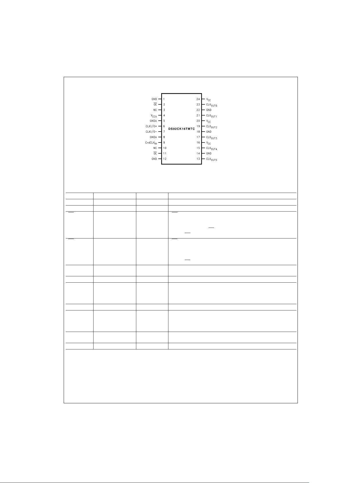
Connection Diagram
TSSOP Package Pin Description
Pin Name Pin # Type Description
CLKI/O+ 6 I/O True (Positive) side of the differential clock input.
CLKI/O− 7 I/O Complementary (Negative) side of the differential clock input.
OE
2 I OE; this pin is active Low. When High, this pin forces all CLK
OUT
pins High. When Low, CLK
OUT
pins logic state is determined by
either the CrdCLK
IN
or the VID at the CLK/I/O pins with respect to
the logic level at the DE pin. This pin has a weak pullup device to
VCC. If OE is floating, then all CLK
OUT
pins will be High.
DE 11 I DE; this pin is active LOW. When Low, this pin enables the
CardCLKINsignal to the CLKI/O pins and CLK
OUT
pins. When High,
the Driver is TRI-STATE
®
, the CLKI/O pins are inputs and determine
the state of the CLK
OUT
pins. This pin has a weak pullup device to
V
CC
. If DE is floating, then CLKI/O pins are TRI-STATE.
CLK
OUT
13, 15, 17, 19, 21,
23
O 6 Buffered clock (CMOS) outputs.
CrdCLK
IN
9 I Input clock from Card (CMOS level or TTL level).
V
CC
16, 20, 24 Power VCC; Analog V
CCA
(Internally separate from VCC, connect externally
or use separate power supplies). No special power sequencing
required. Either V
CCA
or VCCcan be applied first, or simultaneously
apply both power supplies.
GND 1, 12, 14, 18, 22 Ground GND
V
CCA
4 Power Analog V
CCA
(Internally separate from VCC, connect externally or use
separate power supplies). No special power sequencing required.
Either V
CCA
or VCCcan be applied first, or simultaneously apply both
power supplies.
GNDA 5, 8 Ground Analog Ground (Internally separate from Ground must be connected
externally).
NC 3, 10 No Connects
DS101082-2
Order Number DS92CK16TMTC
See NS Package Number MTC24
DS92CK16
www.national.com 2
Page 3
Absolute Maximum Ratings (Note 1)
If Military/Aerospace specified devices are required,
please contact the National Semiconductor Sales Office/
Distributors for availability and specifications.
Supply Voltage (V
CC
) −0.3V to +4V
Enable Input Voltage
(DE, OE, CrdCLK
IN
) −0.3V to +4V
Voltage (CLK
OUT
) −0.3V to (VCC+ 0.3V)
Voltage (CLKI/O
±
) −0.3V to +4V
Driver Short Circuit Current momentary
Receiver Short Circuit Current momentary
Maximum Package Power Dissipation at +25˚C
TSSOP Package 1500 mW
Derate TSSOP Package 8.2 mW/˚C above +25˚C
θ
JA
95˚C/W
θ
JC
30˚C/W
Storage Temperature Range −65˚C to +150˚C
Lead Temperature Range
(Soldering, 4 sec.) 260˚C
ESD Ratings: HBM (Note 2)
>
3000V
CDM (Note 2)
>
1000V
Machine Model (Note 2)
>
200V
Recommended Operating
Conditions
Min Typ Max Units
Supply Voltage (V
CC
) +3.0 +3.3 +3.6 V
CrdCLK
IN
, DE, OE
Input Voltage 0 V
CC
V
Operating Free Air
Temperature (T
A
) −40 25 +85 ˚C
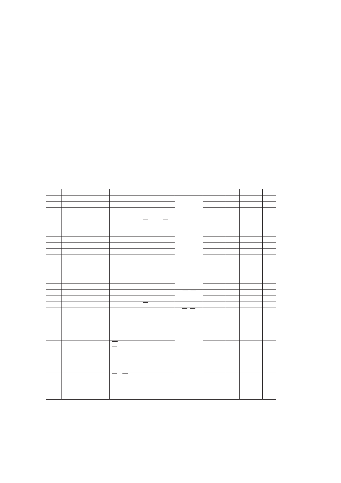
DC Electrical Characteristics
Over Supply Voltage and Operating Temperature ranges, unless otherwise specified (Notes 3, 4).
Symbol Parameter Conditions Pin Min Typ Max Units
V
TH
Input Threshold High CLKI/O+,
CLKI/O−
25 +70 mV
V
TL
Input Threshold Low −70 -35 mV
VCMR Common Mode Voltage
Range (Note 5)
VID=250 mV pk to pk
|VID|/2
2.4 -
|VID|/2
V
I
IN
Input Current V
IN
=
0V to V
CC
,DE=VCC,OE
=
VCC, Other Input=1.2V±50 mV
−20
±
5 +20 µA
V
OH1R
Output High Voltage VID=250 mV, I
OH
=
−1.0 mA CLK
OUT
VCC−0.4 2.9 V
V
OH2R
Output High Voltage VID=250 mV, I
OH
=
−6 mA V
CC
−0.8 2.5 V
V
OL1R
Output Low Voltage I
OL
=
1.0 mA, VID=−250 mV 0.06 0.3 V
V
OL2R
Output Low Voltage I
OL
=
6 mA, VID=−250 mV 0 0.4 V
I
ODHR
CLK
OUT
Dynamic
Output Current (Note 6)
VID=+250 mV, V
OUT
=
V
CC
−1V
−8 -16 -30 mA
I
ODLR
CLK
OUT
Dynamic
Output Current (Note 6)
VID=−250 mV, V
OUT
=
1V
10 21 35 mA
V
IH
Input High Voltage DE, OE,
CrdCLK
IN
2.0 V
CC
V
V
IL
Input Low Voltage GND 0.8 V
I
IH
Input High Current V
IN
=
V
CC
or 2.4V OE, DE −10 −2 +10 µA
I
IL
Input Low Current V
IN
=
GND or 0.4V −20 −5 +20 µA
I
INCRD
Input Current V
IN
=
0V to V
CC
,OE=V
CC
CrdCLK
IN
−5 +5 µA
V
CL
Input Voltage Clamp I
OUT
=
−1.5 mA OE, DE,
CrdCLK
IN
−0.8 V
I
CC
No Load Supply Current
Outputs Enabled, No
VID Applied
OE=DE=0V,
CrdCLK
IN
=
V
CC
or GND,
CLKI/O (
±
)=Open
CLK
OUT
(0:5)=Open Circuit
V
CC
13 mA
I
CC1
No Load Supply Current
Outputs Enabled, VID
over Common Mode
Voltage Range
OE=GND
DE=V
CC
CrdCLK
IN
=
V
CC
or GND,
VID=250 mV
(0.125V VCM 2.275V),
CLK
OUT
(0:5)=Open Circuit
10 mA
I
CCD
Driver Loaded Supply
Current
DE=OE=0V,
CrdCLK
IN
=
V
CC
or GND,
R
L
=
37.5Ω between CLKI/O+ and
CLKI/O−,
CLK
OUT
(0:5)=Open Circuit
20 25 mA
DS92CK16
www.national.com3
Page 4

DC Electrical Characteristics (Continued)
Over Supply Voltage and Operating Temperature ranges, unless otherwise specified (Notes 3, 4).
Symbol Parameter Conditions Pin Min Typ Max Units
V
OD
Driver Output Differential
Voltage
R
L
=
37.5Ω,
Figure 5
DE=0V
CLKI/O+,
CLKI/O−
250 350 450 mV
∆V
OD
Driver VODMagnitude
Change
10 20 mV
V
OS
Driver Offset Voltage 1.1 1.29 1.5 V
∆V
OS
Driver Offset Voltage
Magnitude Change
520mV
V
OHD
Driver Output High 1.35 1.8 V
V
OLD
Driver Output Low 0.80 1.05 V
I
OS1D
Driver Differential Short
Circuit Current (Note 6)
CrdCLK
IN
=
V
CC
or GND, VOD
=
0V, (outputs shorted together)
DE=0V
|30| |50| mA
I
OS2D
Driver Output Short
Circuit Current to V
CC
(Note 6)
CrdCLK
IN
=
GND, DE=0V,
CLKI/O+=V
CC
36 70 mA
I
OS3D
Driver Output Short
Circuit Current to V
CC
(Note 6)
CrdCLK
IN
=
V
CC
,DE=0V,
CLKI/O−=V
CC
34 70 mA
I
OS4D
Driver Output Short
Circuit Current to GND
(Note 6)
CrdCLK
IN
=
V
CC
,DE=0V,
CLKI/O+=0V −47 −70 mA
I
OS5D
Driver Output Short
Circuit Current to GND
(Note 6)
CrdCLK
IN
=
GND, DE=0V,
CLKI/O−=0V −50 −70 mA
I
OFF
Power Off Leakage
Current
V
CC
=
0V or Open,
V
APPLIED
=
3.6V
±
20 µA
Switching Characteristics
Over Supply Voltage and Operating Temperature ranges, unless otherwise specified (Notes 7, 8).
Symbol Parameter Conditions Min Typ Max Units
DIFFERENTIAL RECEIVER CHARACTERISTICS
t
PHLDR
Differential Propagation Delay High to Low. CLKI/O to
CLK
OUT
C
L
=
15 pF
VID=250 mV
Figures 1, 2
1.3 2.8 3.8 ns
t
PLHDR
Differential Propagation Delay Low to High. CLKI/O to
CLK
OUT
1.3 2.9 3.8 ns
t
SK1R
Duty Cycle Distortion(Note 10)
(pulse skew)
|t
PLH–tPHL
|
100 400 ps
t
SK2R
Channel to Channel Skew; Same Edge (Note 11) 30 80 ps
t
SK3R
Part to Part Skew (Note 12) 2.5 ns
t
TLHR
Transition Time Low to High (Note 9)
(20%to 80%)
0.4 1.4 2.4 ns
t
THLR
Transition Time High to Low(Note 9)
(80%to 20%)
0.4 1.3 2.2 ns
t
PLHOER
Propagation Delay Low to High
( OEto CLK
OUT
)
C
L
=
15 pF
Figures 3, 4
1.0 3 4.5 ns
t
PHLOER
Propagation Delay High to Low
(OE to CLK
OUT
)
1.0 3 4.5 ns
f
MAX
Maximum Operating Frequency (Note 15) 100 125 MHz
DS92CK16
www.national.com 4
Page 5

Switching Characteristics (Continued)
Over Supply Voltage and Operating Temperature ranges, unless otherwise specified (Notes 7, 8).
Symbol Parameter Conditions Min Typ Max Units
DIFFERENTIAL DRIVER TIMING REQUIREMENTS
t
PHLDD
Differential Propagation Delay High to Low. CrdCLK
IN
to CLKI/O
C
L
=
15 pF
R
L
=
37.5Ω
Figures 6, 7
0.5 1.8 2.5 ns
t
PLHDD
Differential Propagation Delay Low to High. CrdCLK
IN
to CLKI/O
0.5 1.8 2.5 ns
t
PHLCrd
CrdCLKINto CLK
OUT
Propagation Delay High to Low C
L
=
15 pF
Figures 8, 9
2.0 4.5 6.0 ns
t
PLHCrd
CrdCLKINto CLK
OUT
Propagation Delay Low to High 2.0 4.5 6.0 ns
t
SK1D
Duty Cycle Distortion (pulse skew)
|t
PLH–tPHL
| (Note 13)
600 ps
t
SK2D
Differential Part-to-Part Skew (Note 14) 2.0 ns
t
TLHD
Differential Transition Time (Note 9)
(20%to 80%)
0.4 0.75 1.4 ns
t
THLD
Differential Transition Time (Note 9)
(80%to 20%)
0.4 0.75 1.4 ns
t
PHZD
Transition Time High to TRI-STATE. DE to CLKI/O 10 ns
t
PLZD
Transition Time Low to TRI-STATE. DE to CLKI/O V
IN
=
0V to V
CC
C
L
=
15 pF,
R
L
=
37.5Ω
Figures 10, 11
10 ns
t
PZHD
Transition Time TRI-STATE to High. DE to CLKI/O
32 ns
t
PZLD
Transition Time TRI-STATE to Low. DE to CLKI/O
32 ns
f
MAX
Maximum Operating Frequency (Note 15) 100 125 MHz
Note 1: “Absolute Maximum Ratings” are those values beyond which the safety of the device cannot be guaranteed. These ratings are not meant to imply that the
devices should be operated at these limits. The table of “Electrical Characteristics” specifies conditions of device operation.
Note 2: ESD Rating: ESD qualification is performed per the following: HBM (1.5 kΩ, 100 pF), Machine Model (250V, 0Ω), IEC 1000-4-2. All VCC pins connected to-
gether, all ground pins connected together.
Note 3: Current into device pins is defined as positive. Current out ofdevice pins is defined as negative. All voltages are referenced to ground except VID,VOD, VTH,
and VTL.
Note 4: All typicals are given for: V
CC
= +3.3V and TA= +25˚C.
Note 5: The VCMR range is reduced for larger VID. Example: If VID=400 mV, then VCMR is 0.2V to 2.2VAVIDup to |V
CC
–0V| may be applied between the CLKI/O+
and CLKI/O− inputs, with the Common Mode set to V
CC
/2.
Note 6: Only one output should be momentarily shorted at a time. Do not exceed package power dissipation rating.
Note 7: C
L
includes probe and fixture capacitance.
Note 8: Generator waveform for all tests unless otherwise specified:f=25MHz,Zo = 50Ω,t
r
= 1 ns, tf=1ns(10%–90%). To ensure fastest propagation delay and
minimum skew, clock input edge rates should not be slower than 1 ns/V; control signals not slower than 3 ns/V. In general, the faster the input edge rate, the better
the AC performance.
Note 9: All device output transition times are based on characterization measurements and are guaranteed by design.
Note 10: t
SK1R
is the difference in receiver propagation delay (|t
PLH–tPHL
|) of one device, and is the duty cycle distortion of the output at any given temperature and
V
CC
. The propagation delay specification is a device to device worst case over process, voltage and temperature.
Note 11: t
SK2R
is the difference in receiver propagation delay between channels in the same device of any outputs switching in the same direction. This parameter
is guaranteed by design and characterization.
Note 12: t
SK3R,
part-to-part skew, is the difference in receiver propagation delay between devices of any outputs switching in the same direction. This specification
applies to devices over recommended operating temperature and voltage ranges, and across process distribution. T
SK3R
is defined as Max–Min differential propa-
gation delay.This parameter is guaranteed by design and characterization.
Note 13: t
SK1D
is the difference in driver propagation delay (|t
PLH–tPHL
|) and is the duty cycle distortion of the CLKI/O outputs.
Note 14: t
SK2D
part-to-part skew, is the difference in driver propagation delay between devices of any outputs switching in the same direction. This specification ap-
plies to devices over recommended operating temperature and voltage ranges, and across process distribution. t
SK2D
is defined as Max–Min differential propagation
delay.
Note 15: Generator input conditions: t
r/tf
<
1 ns, 50%duty cycle, differential (1.10V to 1.35V pk-pk). Output Criteria: 60%/40%duty cycle, VOL(max) 0.4V, VOH(min)
2.7V, Load=7pF(stray plus probes).
DS92CK16
www.national.com5
Page 6

Parameter Measurement Information
DS101082-3
FIGURE 1. Receiver Propagation Delay and Transition Time Test Circuit
DS101082-4
Generator waveform for all test unless otherwise specified: f=25 MHz, 50%Duty Cycle, Zo=50Ω,t
TLH
=
1 ns, t
THL
=
1 ns.
FIGURE 2. Receiver Propagation Delay and Transition Time Waveforms
DS101082-5
FIGURE 3. Output Enable (OE) Delay Test Circuit
DS101082-6
FIGURE 4. Output Enable (OE) Delay Waveforms
DS92CK16
www.national.com 6
Page 7

Parameter Measurement Information (Continued)
DS101082-7
FIGURE 5. Differential Driver DC Test
DS101082-8
FIGURE 6. Driver Propagation Delay Test Circuit
DS101082-9
FIGURE 7. Driver Propagation Delay and Transition Time Waveforms
DS101082-10
FIGURE 8. CrdCLKINPropagation Delay Time Test Circuit
DS92CK16
www.national.com7
Page 8

Parameter Measurement Information (Continued)
DS101082-11
FIGURE 9. CrdCLKINPropagation Delay Time Waveforms
DS101082-12
FIGURE 10. Driver TRI-STATE Test Circuit
DS101082-13
FIGURE 11. Driver TRI-STATE Waveforms
DS92CK16
www.national.com 8
Page 9

Applications Information
General application guidelines and hints for BLVDS/LVDS
transceivers, drivers and receivers may be found in the following application notes: LVDS Owner’s Manual (lit
#550062-001), AN805, AN807, AN808, AN903, AN905,
AN916, AN971, AN977 .
BLVDS drivers and receivers are intended to be used in a
differential backplane configuration. Transceivers or receivers are connected to the driver through a balanced media
such as differential PCB traces. Typically, the characteristic
differential impedance of the media (Zo) is in the range of
50Ω to100Ω. Two termination resistors of ZoΩ each are
placed at the ends of the transmission line backplane. The
termination resistor converts the current sourced by the
driver into a voltage that is detected by the receiver. The effects of mid-stream connector(s), cable stub(s), and other
impedance discontinuities as well as ground shifting, noise
margin limits, and total termination loading must be taken
into account.
The DS92CK16 differential line driver is a balanced current
source design. A current mode driver, generally speaking
has a high output impedance (100 ohms) and supplies a
constant current for a range of loads (a voltage mode driver
on the other hand supplies a constant voltage for a range of
loads). Current is switched through the load in one direction
to produce a logic state and in the other direction to produce
the other logic state. The output current is typically 9.330
mA. The current changes as a function of load resistor.The
current mode requires (as discussed above) that a resistive
termination be employed to terminate the signal and to complete the loop. Unterminated configurations are not allowed.
The 9.33 mA loop current will develop a differential voltage of
about 350mV across 37.5Ω (double terminated 75Ω differential transmission backplane) effective resistance, which the
receiver detects with a 280 mV minimum differential noise
margin neglecting resistive line losses (driven signal minus
receiver threshold (350 mV – 70 mV=280 mV)). The signal
is centered around +1.2V (Driver Offset, V
OS
) with respect to
ground. Note that the steady-state voltage (V
SS
)
peak-to-peak swing is twice the differential voltage (V
OD
)
and is typically 700 mV.
The current mode driver provides substantial benefits over
voltage mode drivers, such as an RS-422 driver. Its quiescent current remains relatively flat versus switching frequency.Whereas the RS-422 voltage mode driver increases
exponentially in most case between 20 MHz–50 MHz. This
is due to the overlap current that flows between the rails of
the device when the internal gates switch. Whereas the current mode driver switches a fixed current between its output
without any substantial overlap current. This is similar to
some ECL and PECL devices, but without the heavy static
I
CC
requirements of the ECL/PECL designs. LVDS requires
>
80%less current than similar PECL devices.AC specifications for the driver are a tenfold improvement over other existing RS-422 drivers.
The TRI-STATE function allows the driver outputs to be disabled, thus obtaining an even lower power state when the
transmission of data is not required.
Power Decoupling Recommendations:
Bypass capacitors must be used on power pins. High frequency ceramic (surface mount is recommended) 0.1µF in
parallel with 0.01µF, in parallel with 0.001µF at the power
supply pin as well as scattered capacitors over the printed
circuit board. Multiple vias should be used to connect the de-
coupling capacitors to the power planes. A 4.7µF (35V) or
greater solid tantalum capacitor should be connected at the
power entry point on the printed circuit board.
PC Board considerations:
Use at least 4 PCB layers (top to bottom); BLVDS signals,
ground, power, TTL signals.
Isolate TTL signals from BLVDS signals, otherwise the TTL
may couple onto the BLVDS lines. It is best to put TTL and
BLVDS signals on different layers which are isolated by a
power/ground plane(s).
Keep drivers and receivers as close to the (BLVDSport side)
connectors as possible to create short stub lengths.
Differential Traces:
Use controlled impedance traces which match the differential impedance of your transmission medium (ie. backplane
or cable) and termination resistor(s). Run the differential pair
trace lines as close together as possible as soon as they
leave the IC . This will help eliminate reflections and ensure
noise is coupled as common-mode. In fact, we have seen
that differential signals which are 1mm apart radiate far less
noise than traces 3mm apart since magnetic field cancellation is much better with the closer traces. Plus, noise induced on the differential lines is much more likely to appear
as common-mode which is rejected by the receiver.
Match electrical lengths between traces to reduce skew.
Skew between the signals of a pair means a phase difference between signals which destroys the magnetic field cancellation benefits of differential signals and EMI will result.
(Note the velocity of propagation, v = c/Er where c (the
speed of light) = 0.2997mm/ps or 0.0118 in/ps). Do not rely
solely on the autoroute function for differential traces. Carefully review dimensions to match differential impedance and
provide isolation for the differential lines. Minimize the number or vias and other discontinuities on the line.
Avoid 90˚ turns (these cause impedance discontinuities).
Use arcs or 45˚ bevels.
Within a pair of traces, the distance between the two traces
should be minimized to maintain common-mode rejection of
the receivers. On the printed circuit board, this distance
should remain constant to avoid discontinuities in differential
impedance. Minor violations at connection points are allowable.
Stub Length:
Stub lengths should be kept to a minimum. The typical transition time of the DS92CK16 BLVDS output is 0.75ns (20
%
to 80%). The 100 percent time is 0.75/0.6 or 1.25ns. For a
general approximation, if the electrical length of a trace is
greater than 1/5 of the transition edge, then the trace is considered a transmission line. For example, 1.25ns/5 is 250 picoseconds. Let velocity equal 160ps per inch for a typical
loaded backplane. Then maximum stub length is
250ps/160ps/in or 1.56 inches. To determine the maximum
stub for your backplane, you need to know the propagation
velocity for the actual conditions (refer to application notes
AN 905 and AN 808).
DS92CK16
www.national.com9
Page 10

Applications Information (Continued)
Termination:
Use a resistor which best matches the differential impedance
of your loaded transmission line. Remember that the current
mode outputs need the termination resistor to generate the
differential voltage. BLVDS will not work without resistor termination.
Surface mount 1%to 2%resistors are best.
Probing BLVDS Transmission Lines:
Always use high impedance (
>
100kΩ), low capacitance
(
<
2pF) scope probes with a wide bandwidth (1GHz) scope.
Improper probing will give deceiving results.
Cables and Connectors, General Comments:
Use controlled impedance media. The connectors you use
should have a matched differential impedance of about
Zo Ω. They should not introduce major impedance discontinuities.
Balanced cables (e.g. twisted pair) are usually better than
unbalanced cables (ribbon cable, simple coax.) for noise reduction and signal quality. Balanced cables tend to generate
less EMI due to field canceling effects and also tend to pick
up electromagnetic radiation a common-mode (not differential mode) noise which is rejected by the receiver. For cable
distances
<
0.5M, most cables can be made to work effectively. For distances 0.5M ≤ d ≤ 10M, CAT 3 (category 3)
twisted pair cable works well, is readily available and relatively inexpensive.
DS92CK16
www.national.com 10
Page 11

Physical Dimensions
LIFE SUPPORT POLICY
NATIONAL’S PRODUCTS ARE NOT AUTHORIZED FOR USE AS CRITICAL COMPONENTS IN LIFE SUPPORT
DEVICES OR SYSTEMS WITHOUT THE EXPRESS WRITTEN APPROVAL OF THE PRESIDENT AND GENERAL
COUNSEL OF NATIONAL SEMICONDUCTOR CORPORATION. As used herein:
1. Life support devices or systems are devices or
systems which, (a) are intended for surgical implant
into the body, or (b) support or sustain life, and
whose failure to perform when properly used in
accordance with instructions for use provided in the
labeling, can be reasonably expected to result in a
significant injury to the user.
2. A critical component is any component of a life
support device or system whose failure to perform
can be reasonably expected to cause the failure of
the life support device or system, or to affect its
safety or effectiveness.
National Semiconductor
Corporation
Americas
Tel: 1-800-272-9959
Fax: 1-800-737-7018
Email: support@nsc.com
National Semiconductor
Europe
Fax: +49 (0) 1 80-530 85 86
Email: europe.support@nsc.com
Deutsch Tel: +49 (0) 1 80-530 85 85
English Tel: +49 (0) 1 80-532 78 32
Français Tel: +49 (0) 1 80-532 93 58
Italiano Tel: +49 (0) 1 80-534 16 80
National Semiconductor
Asia Pacific Customer
Response Group
Tel: 65-2544466
Fax: 65-2504466
Email: sea.support@nsc.com
National Semiconductor
Japan Ltd.
Tel: 81-3-5639-7560
Fax: 81-3-5639-7507
www.national.com
24-Pin TSSOP Package Drawing
Dimensions shown in millimeters
Order Number DS92CK16TMTC
NS Package Number MTC24
DS92CK16 3V BLVDS 1 to 6 Clock Buffer/Bus Transceiver
National does not assume any responsibility for use of any circuitry described, no circuit patent licenses are implied and National reserves the right at any time without notice to change said circuitry and specifications.
 Loading...