

Page 1
DS90LV048A
3V LVDS Quad CMOS Differential Line Receiver
General Description
The DS90LV048Ais a quad CMOS flow-through differential
line receiver designed for applications requiring ultra low
power dissipation and high data rates. The device is designed to support data rates in excess of 400 Mbps (200
MHz) utilizing Low Voltage Differential Signaling (LVDS)
technology.
The DS90LV048A accepts low voltage (350 mV typical) differential input signals and translates them to 3V CMOS output levels. The receiver supports a TRI-STATE
®
function that
may be used to multiplex outputs. The receiver also supports
open, shorted and terminated (100Ω) input fail-safe. The receiver output will be HIGH for all fail-safe conditions. The
DS90LV048Ahasaflow-through pinout for easy PCB layout.
The EN and EN
*
inputs are ANDed together and control the
TRI-STATE outputs. The enables are common to all four receivers. The DS90LV048Aand companion LVDS line driver
(eg. DS90LV047A) provide a new alternative to high power
PECL/ECL devices for high speed point-to-point interface
applications.
Features
n
>
400 Mbps (200 MHz) switching rates
n Flow-through pinout simplifies PCB layout
n 150 ps channel-to-channel skew (typical)
n 100 ps differential skew (typical)
n 2.7 ns maximum propagation delay
n 3.3V power supply design
n High impedance LVDS inputs on power down
n Low Power design (40mW 3.3V static)
n Interoperable with existing 5V LVDS drivers
n Accepts small swing (350 mV typical) differential signal
levels
n Supports open, short and terminated input fail-safe
n Conforms to ANSI/TIA/EIA-644 Standard
n Industrial temperature operating range (-40˚C to +85˚C)
n Available in SOIC and TSSOP package
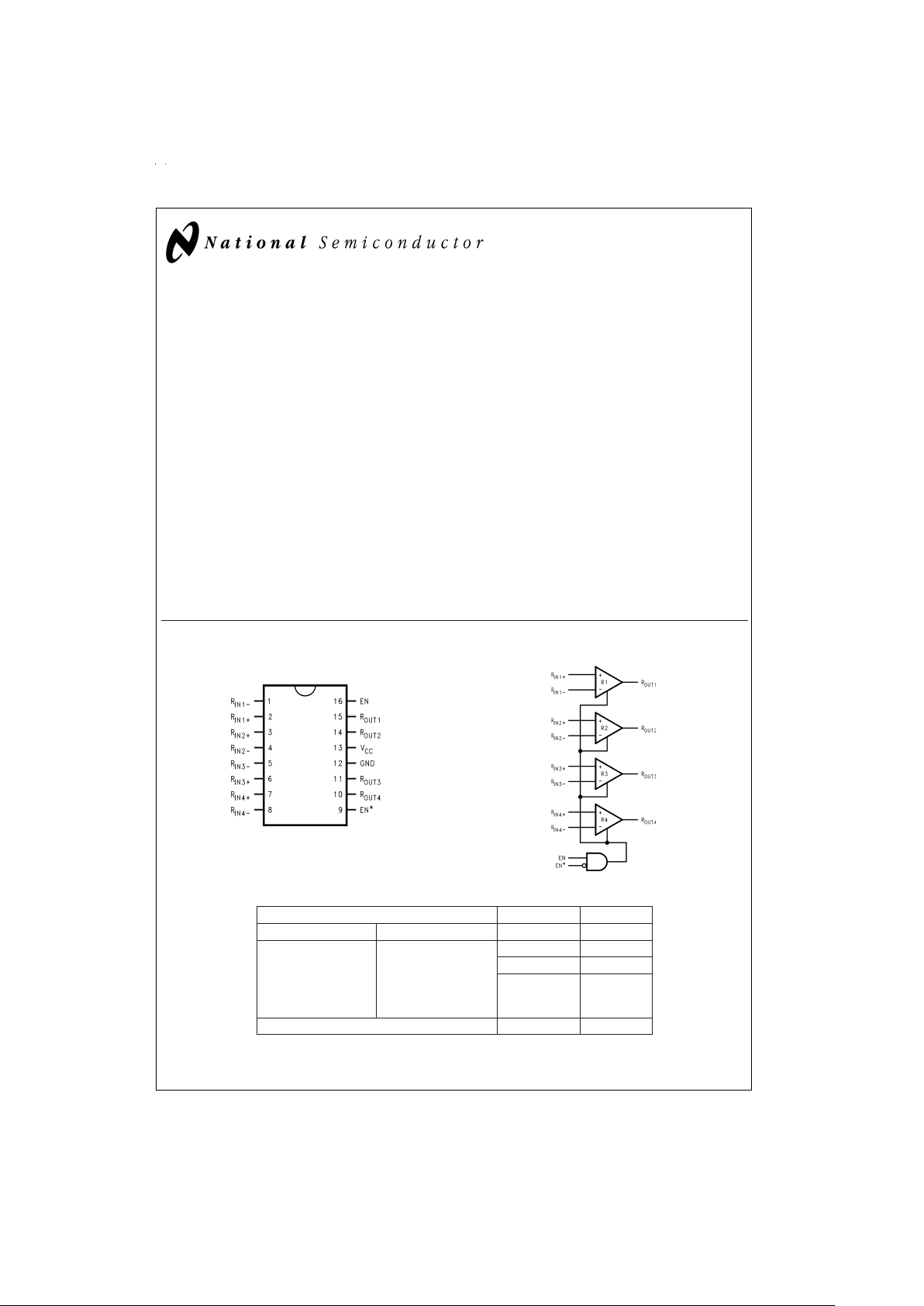
Connection Diagram Functional Diagram
ENABLES INPUTS OUTPUT
EN EN* R
IN+−RIN−
R
OUT
H L or Open VID≥ 0.1V H
V
ID
≤ −0.1V L
Full Fail-safe
OPEN/SHORT
or Terminated
H
All other combinations of ENABLE inputs X Z
TRI-STATE®is a registered trademark of National Semiconductor Corporation.
Dual-in-Line
DS100888-1
Order Number DS90LV048ATM, DS90LV048ATMTC
See NS Package Number M16A, MTC16
DS100888-2
July 1999
DS90LV048A 3V LVDS Quad CMOS Differential Line Receiver
© 1999 National Semiconductor Corporation DS100888 www.national.com
Page 2
Absolute Maximum Ratings (Note 1)
If Military/Aerospace specified devices are required,
please contact the National Semiconductor Sales Office/
Distributors for availability and specifications.
Supply Voltage (V
CC
) −0.3V to +4V
Input Voltage (R
IN+,RIN−
) −0.3V to 3.9V
Enable Input Voltage (EN, EN*) −0.3V to (V
CC
+ 0.3V)
Output Voltage (R
OUT
) −0.3V to (VCC+ 0.3V)
Maximum Package Power Dissipation +25˚C
M Package 1025 mW
MTC Package 866 mW
Derate M Package 8.2 mW/˚C above +25˚C
Derate MTC Package 6.9 mW/˚C above +25˚C
Storage Temperature Range −65˚C to +150˚C
Lead Temperature Range Soldering
(4 sec.) +260˚C
Maximum Junction Temperature +150˚C
ESD Rating (Note 10)
(HBM, 1.5 kΩ, 100 pF) ≥ 10 kV
(EIAJ, 0 Ω, 200 pF) ≥ 1200 V
Recommended Operating
Conditions
Min Typ Max Units
Supply Voltage (V
CC
) +3.0 +3.3 +3.6 V
Receiver Input Voltage GND +3.0 V
Operating Free Air
Temperature (T
A
) −40 25 +85 ˚C
Electrical Characteristics
Over Supply Voltage and Operating Temperature ranges, unless otherwise specified. (Notes 2, 3)
Symbol Parameter Conditions Pin Min Typ Max Units
V
TH
Differential Input High Threshold VCM= +1.2V, 0.05V, 2.95V (Note 13) R
IN+
, +100 mV
V
TL
Differential Input Low Threshold R
IN−
−100 mV
VCMR Common-Mode Voltage Range VID=200mV pk to pk (Note 5) 0.1 2.3 V
I
IN
Input Current VIN= +2.8V VCC= 3.6V or 0V −10
±
5 +10 µA
V
IN
= 0V −10
±
1 +10 µA
V
IN
= +3.6V VCC= 0V -20
±
1 +20 µA
V
OH
Output High Voltage IOH= −0.4 mA, VID= +200 mV R
OUT
2.7 3.3 V
I
OH
= −0.4 mA, Input terminated 2.7 3.3 V
I
OH
= −0.4 mA, Input shorted 2.7 3.3 V
V
OL
Output Low Voltage IOL= 2 mA, VID= −200 mV 0.05 0.25 V
I
OS
Output Short Circuit Current Enabled, V
OUT
= 0V (Note 11) −15 −47 −100 mA
I
OZ
Output TRI-STATE Current Disabled, V
OUT
=0VorV
CC
−10
±
1 +10 µA
V
IH
Input High Voltage EN,
EN*
2.0 V
CC
V
V
IL
Input Low Voltage GND 0.8 V
I
I
Input Current VIN=0VorVCC, Other Input = VCCor
GND
−10
±
5 +10 µA
V
CL
Input Clamp Voltage ICL= −18 mA −1.5 −0.8 V
I
CC
No Load Supply Current
Receivers Enabled
EN=VCC, Inputs Open V
CC
915mA
I
CCZ
No Load Supply Current EN = GND, Inputs Open 1 5 mA
Receivers Disabled
Switching Characteristics
Over Supply Voltage and Operating Temperature ranges, unless otherwise specified. (Notes 3, 4, 7, 8)
Symbol Parameter Conditions Min Typ Max Units
t
PHLD
Differential Propagation Delay High to Low CL= 15 pF 1.2 2.0 2.7 ns
t
PLHD
Differential Propagation Delay Low to High VID= 200 mV 1.2 1.9 2.7 ns
t
SKD1
Differential Pulse Skew |t
PHLD−tPLHD
| (Note 6) (
Figure 1
and
Figure 2
) 0 0.1 0.4 ns
t
SKD2
Differential Channel-to-Channel Skew; same device
(Note 7)
0 0.15 0.5 ns
t
SKD3
Differential Part to Part Skew (Note 8) 1.0 ns
t
SKD4
Differential Part to Part Skew (Note 9) 1.5 ns
t
TLH
Rise Time 0.5 1.0 ns
t
THL
Fall Time 0.35 1.0 ns
www.national.com 2
Page 3
Switching Characteristics (Continued)
Over Supply Voltage and Operating Temperature ranges, unless otherwise specified. (Notes 3, 4, 7, 8)
Symbol Parameter Conditions Min Typ Max Units
t
PHZ
Disable Time High to Z RL=2kΩ 814ns
t
PLZ
Disable Time Low to Z CL=15pF 8 14 ns
t
PZH
Enable Time Z to High (
Figure 3
and
Figure 4
) 9 14 ns
t
PZL
Enable Time Z to Low 914ns
f
MAX
Maximum Operating Frequency (Note 14) All Channels Switching 200 250 MHz
Note 1: “Absolute Maximum Ratings” are those values beyond which the safety of the device cannot be guaranteed. They are not meant to imply that the devices
should be operated at these limits. The table of “Electrical Characteristics” specifies conditions of device operation.
Note 2: Currentintodevice pins is defined as positive. Currentoutofdevicepins is defined as negative.Allvoltagesarereferenced to ground unless otherwise specified.
Note 3: All typicals are given for: V
CC
= +3.3V, TA= +25˚C.
Note 4: Generator waveform for all tests unless otherwise specified:f=1MHz, Z
O
=50Ω,trand tf(0%to 100%) ≤ 3 ns for RIN.
Note 5: TheVCMRrangeisreducedforlargerVID.Example:ifVID=400mV,theVCMRis0.2Vto2.2V. The fail-safe condition with inputs shorted is not supported
over the common-mode range of 0V to 2.4V,but is supported only with inputs shorted and no external common-mode voltage applied. A VID up to V
CC
− 0V may be
applied to the R
IN+/RIN−
inputs with the Common-Mode voltage set to VCC/2. Propagation delay and Differential Pulse skew decrease when VID is increased from
200mV to 400mV. Skew specifications apply for 200mV ≤ VID ≤ 800mV over the common-mode range .
Note 6: t
SKD1
is the magnitude difference in differential propagation delay time between the positive going edge and the negative going edge of the same channel
Note 7: t
SKD2
, Channel-to-Channel Skew is defined as the difference between the propagation delay of one channel and that of the others on the same chip with
any event on the inputs.
Note 8: t
SKD3
, part to part skew, is the differential channel-to-channel skew of any event between devices. This specification applies to devices at the same VCC,
and within 5˚C of each other within the operating temperature range.
Note 9: t
SKD4
, part to part skew, is the differential channel-to-channel skew of any event between devices. This specification applies to devices over recommended
operating temperature and voltage ranges, and across process distribution. t
SKD4
is defined as |Max−Min| differential propagation delay.
Note 10: ESD Rating:HBM (1.5 kΩ, 100 pF) ≥ 10kV
EIAJ (0Ω, 200 pF) ≥ 1200V
Note 11: Output short circuit current (I
OS
) is specified as magnitude only, minus sign indicates direction only. Only one output should be shorted at a time, do not
exceed maximum junction temperature specification.
Note 12: C
L
includes probe and jig capacitance.
Note 13: V
CC
is always higher than R
IN+
and R
IN−
voltage. R
IN−
and R
IN+
are allowed to have a voltage range −0.2V to VCC− VID/2. However, to be compliant with
AC specifications, the common voltage range is 0.1V to 2.3V
Note 14: f
MAX
generator input conditions: t
r
=
t
f
<
1ns(0%to 100%), 50%duty cycle, differential (1.05V to 1.35V peak to peak). Output criteria: 60/40%duty cycle,
V
OL
(max 0.4V), VOH(min 2.7V), Load=15 pF (stray plus probes).
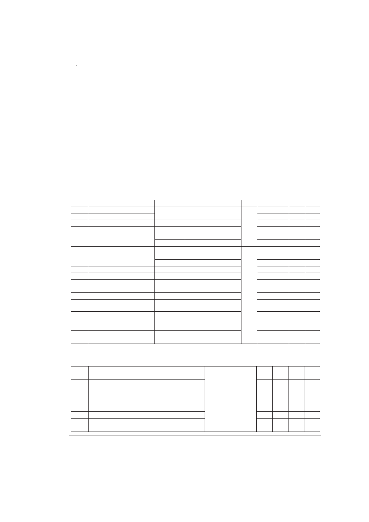
Parameter Measurement Information
DS100888-3
FIGURE 1. Receiver Propagation Delay and Transition Time Test Circuit
DS100888-4
FIGURE 2. Receiver Propagation Delay and Transition Time Waveforms
www.national.com3
Page 4
Parameter Measurement Information (Continued)
Typical Application
Applications Information
General application guidelines and hints for LVDS drivers
and receivers may be found in the following application
notes: LVDS Owner’s Manual (lit #550062-001), AN808,
AN977, AN971, AN916, AN805, AN903.
LVDSdriversand receivers are intendedto be primarily used
in an uncomplicated point-to-point configuration as is shown
in
Figure 5
. This configuration provides a clean signaling environment for the fast edge rates of the drivers. The receiver
is connected to the driver through a balanced media which
may be a standard twisted pair cable, a parallel pair cable, or
simply PCB traces. Typically,the characteristic impedance of
the media is in the range of 100Ω. A termination resistor of
100Ω (selected to match the media), and is located as close
to the receiver input pins as possible. The termination resistor converts the driver output (current mode) into a voltage
that is detected by the receiver. Other configurations are
possible such as a multi-receiver configuration, but the effects of a mid-stream connector(s), cable stub(s), and other
impedance discontinuities as well as ground shifting, noise
margin limits, and total termination loading must be taken
into account.
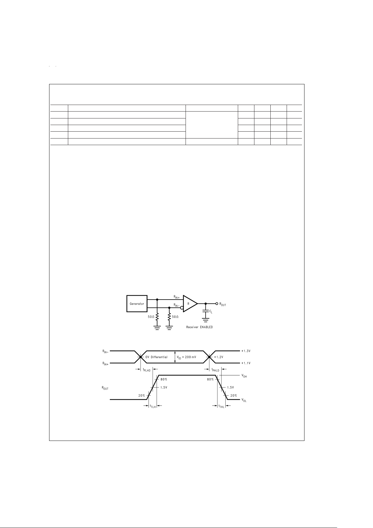
DS100888-5
CLincludes load and test jig capacitance.
S
1=VCC
for t
PZL
and t
PLZ
measurements.
S
1
= GND for t
PZH
and t
PHZ
measurements.
FIGURE 3. Receiver TRI-STATE Delay Test Circuit
DS100888-6
FIGURE 4. Receiver TRI-STATE Delay Waveforms
Balanced System
DS100888-7
FIGURE 5. Point-to-Point Application
www.national.com 4
Page 5

Applications Information (Continued)
The DS90LV048A differential line receiver is capable of detecting signals as low as 100mV, over a
±
1V common-mode
range centered around +1.2V. This is related to the driver offset voltage which is typically +1.2V.The driven signal is centered around this voltage and may shift
±
1V around this cen-
ter point. The
±
1V shifting may be the result of a ground
potential difference between the driver’s ground reference
and the receiver’s ground reference, the common-mode effects of coupled noise, or a combination of the two. The AC
parameters of both receiver input pins are optimized for a
recommended operating input voltage range of 0V to +2.4V
(measured from each pin to ground). The device will operate
for receiver input voltages up to V
CC
, but exceeding VCCwill
turn on the ESD protection circuitry which will clamp the bus
voltages.
The DS90LV048A has a flow-through pinout that allows for
easy PCB layout. The LVDS signals on one side of the device easily allows for matching electrical lengths of the differential pair trace lines between the driver and the receiver as
well as allowing the trace lines to be close together to couple
noise as common-mode. Noise isolation is achieved with the
LVDS signals on one side of the device and the TTL signals
on the other side.
Power Decoupling Recommendations:
Bypass capacitors must be used on power pins. Use high
frequency ceramic (surface mount is recommended) 0.1µF
and 0.001µF capacitors in parallel at the power supply pin
with the smallest value capacitor closest to the device supply
pin. Additional scattered capacitors over the printed circuit
board will improve decoupling. Multiple vias should be used
to connect the decoupling capacitors to the power planes. A
10µF (35V) or greater solid tantalum capacitor should be
connected at the power entry point on the printed circuit
board between the supply and ground.
PC Board considerations:
Use at least 4 PCB layers (top to bottom); LVDS signals,
ground, power, TTL signals.
Isolate TTL signals from LVDS signals, otherwise the TTL
may couple onto the LVDS lines. It is best to put TTL and
LVDS signals on different layers which are isolated by a
power/ground plane(s)
Keep drivers and receivers as close to the (LVDS port side)
connectors as possible.
Differential Traces:
Use controlled impedance traces which match the differential impedance of your transmission medium (ie. cable) and
termination resistor. Run the differential pair trace lines as
close together as possible as soon as they leave the IC
(stubs should be
<
10mm long). This will help eliminate reflections and ensure noise is coupled as common-mode. In
fact, we have seen that differential signals which are 1mm
apart radiate far less noise than traces 3mm apart since
magnetic field cancellation is much better with the closer
traces. In addition, noise induced on the differential lines is
much more likely to appear as common-mode which is rejected by the receiver.
Match electrical lengths between traces to reduce skew.
Skew between the signals of a pair means a phase difference between signals which destroys the magnetic field cancellation benefits of differential signals and EMI will result.
(Note the velocity of propagation, v = c/Er where c (the
speed of light) = 0.2997mm/ps or 0.0118 in/ps). Do not rely
solely on the autoroute function for differential traces. Care-
fully review dimensions to match differential impedance and
provide isolation for the differential lines. Minimize the number or vias and other discontinuities on the line.
Avoid 90˚ turns (these cause impedance discontinuities).
Use arcs or 45˚ bevels.
Within a pair of traces, the distance between the two traces
should be minimized to maintain common-mode rejection of
the receivers. On the printed circuit board, this distance
should remain constant to avoid discontinuities in differential
impedance. Minor violations at connection points are allowable.
Termination:
Use a termination resistor which best matches the differential impedance or your transmission line. The resistor should
be between 90Ω and 130Ω. Remember that the current
mode outputs need the termination resistor to generate the
differential voltage. LVDS will not work without resistor termination. Typically, connecting a single resistor across the pair
at the receiver end will suffice.
Surface mount 1%to 2%resistors are best. PCB stubs,
component lead, and the distance from the termination to the
receiver inputs should be minimized. The distance between
the termination resistor and the receiver should be
<
10mm
(12mm MAX)
Probing LVDS Transmission Lines:
Always use high impedance (
>
100kΩ), low
capacitance (
<
2 pF) scope probes with a wide bandwidth (1
GHz) scope. Improper probing will give deceiving results.
Cables and Connectors, General Comments:
When choosing cable and connectors for LVDS it is important to remember:
Use controlled impedance media. The cables and connectors you use should have a matched differential impedance
of about 100Ω. They should not introduce major impedance
discontinuities.
Balanced cables (e.g. twisted pair) are usually better than
unbalanced cables (ribbon cable, simple coax.) for noise reduction and signal quality. Balanced cables tend to generate
less EMI due to field canceling effects and also tend to pick
up electromagnetic radiation a common-mode (not differential mode) noise which is rejected by the receiver.
For cable distances
<
0.5M, most cables can be made to
work effectively. For distances 0.5M ≤ d ≤ 10M, CAT 3 (category 3) twisted pair cable works well, is readily available
and relatively inexpensive.
Fail-Safe Feature:
The LVDS receiver is a high gain, high speed device that
amplifies a small differential signal (20mV) to CMOS logic
levels. Due to the high gain and tight threshold of the receiver,care should be taken to prevent noise from appearing
as a valid signal.
The receiver’s internal fail-safe circuitry is designed to
source/sink a small amount of current, providing fail-safe
protection (a stable known state of HIGH output voltage) for
floating, terminated or shorted receiver inputs.
1. Open Input Pins. The DS90LV048Ais a quad receiver
device, and if an application requires only 1, 2 or 3 receivers, the unused channel(s) inputs should be left
OPEN. Do not tie unused receiver inputs to ground or
any other voltages. The input is biased by internal high
value pull up and pull down resistors to set the output to
a HIGH state. This internal circuitry will guarantee a
HIGH, stable output state for open inputs.
www.national.com5
Page 6

Applications Information (Continued)
2. Terminated Input. If the driver is disconnected (cable
unplugged), or if the driver is in a TRI-STATE or poweroff condition, the receiver output will again be in a HIGH
state, even with the end of cable 100Ω termination resistor across the input pins. The unplugged cable can become a floating antenna which can pick up noise. If the
cable picks up more than 10mV of differential noise, the
receiver may see the noise as a valid signal and switch.
To insure that any noise is seen as common-mode and
not differential, a balanced interconnect should be used.
Twisted pair cable will offer better balance than flat ribbon cable.
3. Shorted Inputs. If a fault condition occurs that shorts
the receiver inputs together, thus resulting in a 0V differential input voltage, the receiver output will remain in a
HIGH state. Shorted input fail-safe is not supported
across the common-mode range of the device (GND to
2.4V). It is only supported with inputs shorted and no external common-mode voltage applied.
External lower value pull up and pull down resistors (for a
stronger bias) may be used to boost fail-safe in the presence
of higher noise levels. The pull up and pull down resistors
should be in the 5kΩ to 15kΩ range to minimize loading and
waveform distortion to the driver. The common-mode bias
point should be set to approximately 1.2V (less than 1.75V)
to be compatible with the internal circuitry.
Pin Descriptions
Pin No. Name Description
2, 3, 6, 7 R
IN+
Non-inverting receiver input pin
1, 4, 5, 8 R
IN−
Inverting receiver input pin
10, 11, 14, R
OUT
Receiver output pin
15
16 EN Receiver enable pin: When EN is
low, the receiver is disabled.
When EN is high and EN* is low
or open, the receiver is enabled.
If both EN and EN* are open
circuit, then the receiver is
disabled.
9 EN* Receiver enable pin: When EN*
is high, the receiver is disabled.
When EN* is low or open and
EN is high, the receiver is
enabled. If both EN and EN* are
open circuit, then the receiver is
disabled.
13 V
CC
Power supply pin, +3.3V±0.3V
12 GND Ground pin
Ordering Information
Operating Package Type/ Order Number
Temperature Number
−40˚C to +85˚C SOP/M16A DS90LV048ATM
−40˚C to +85˚C TSSOP/MTC16 DS90LV048ATMTC
Typical Performance Curves
Output High Voltage vs
Power Supply Voltage
DS100888-12
Output Low Voltage vs
Power Supply Voltage
DS100888-13
www.national.com 6
Page 7

Typical Performance Curves (Continued)
Output Short Circuit Current vs
Power Supply Voltage
DS100888-14
Output TRI-STATE Current vs
Power Supply Voltage
DS100888-15
Differential Transition Voltage vs
Power Supply Voltage
DS100888-16
Power Supply Current
vs Frequency
DS100888-17
Power Supply Current vs
Ambient Temperature
DS100888-18
Differential Propagation Delay vs
Power Supply Voltage
DS100888-19
www.national.com7
Page 8

Typical Performance Curves (Continued)
Differential Propagation Delay vs
Ambient Temperature
DS100888-20
Differential Propagation Delay vs
Differential Input Voltage
DS100888-21
Differential Propagation Delay vs
Common-Mode Voltage
DS100888-22
Differential Skew vs
Power Supply Voltage
DS100888-23
Differential Skew vs
Ambient Temperature
DS100888-24
Transition Time vs
Power Supply Voltage
DS100888-25
www.national.com 8
Page 9

Typical Performance Curves (Continued)
Transition Time vs
Ambient Temperature
DS100888-26
www.national.com9
Page 10

Physical Dimensions inches (millimeters) unless otherwise noted
16-Lead (0.150" Wide) Molded Small Outline Package, JEDEC
Order Number DS90LV048ATM
NS Package Number M16A
www.national.com 10
Page 11

Physical Dimensions inches (millimeters) unless otherwise noted (Continued)
LIFE SUPPORT POLICY
NATIONAL’S PRODUCTS ARE NOT AUTHORIZED FOR USE AS CRITICAL COMPONENTS IN LIFE SUPPORT
DEVICES OR SYSTEMS WITHOUT THE EXPRESS WRITTEN APPROVAL OF THE PRESIDENT AND GENERAL
COUNSEL OF NATIONAL SEMICONDUCTOR CORPORATION. As used herein:
1. Life support devices or systems are devices or
systems which, (a) are intended for surgical implant
into the body, or (b) support or sustain life, and
whose failure to perform when properly used in
accordance with instructions for use provided in the
labeling, can be reasonably expected to result in a
significant injury to the user.
2. A critical component is any component of a life
support device or system whose failure to perform
can be reasonably expected to cause the failure of
the life support device or system, or to affect its
safety or effectiveness.
National Semiconductor
Corporation
Americas
Tel: 1-800-272-9959
Fax: 1-800-737-7018
Email: support@nsc.com
National Semiconductor
Europe
Fax: +49 (0) 1 80-530 85 86
Email: europe.support@nsc.com
Deutsch Tel: +49 (0) 1 80-530 85 85
English Tel: +49 (0) 1 80-532 78 32
Français Tel: +49 (0) 1 80-532 93 58
Italiano Tel: +49 (0) 1 80-534 16 80
National Semiconductor
Asia Pacific Customer
Response Group
Tel: 65-2544466
Fax: 65-2504466
Email: sea.support@nsc.com
National Semiconductor
Japan Ltd.
Tel: 81-3-5639-7560
Fax: 81-3-5639-7507
www.national.com
16-Lead (0.100" Wide) Molded Thin Shrink Small Outline Package, JEDEC
Order Number DS90LV048ATMTC
NS Package Number MTC16
DS90LV048A 3V LVDS Quad CMOS Differential Line Receiver
National does not assume any responsibility for use of any circuitry described, no circuit patent licenses are implied and National reserves the right at any time without notice to change said circuitry and specifications.
 Loading...