

Page 1
DS90LV048A
3V LVDS Quad CMOS Differential Line Receiver
DS90LV048A 3V LVDS Quad CMOS Differential Line Receiver
May 2001
General Description
The DS90LV048Ais a quad CMOS flow-through differential
line receiver designed for applications requiring ultra low
power dissipation and high data rates. The device is designed to support data rates in excess of 400 Mbps (200
MHz) utilizing Low Voltage Differential Signaling (LVDS)
technology.
The DS90LV048A accepts low voltage (350 mV typical) differential input signals and translates them to 3V CMOS
output levels. The receiver supports a TRI-STATE
that may be used to multiplex outputs. The receiver also
supports open, shorted and terminated (100Ω) input failsafe. The receiver output will be HIGH for all fail-safe conditions. The DS90LV048A has a flow-through pinout for easy
PCB layout.
The EN and EN
TRI-STATE outputs. The enables are common to all four
receivers. The DS90LV048A and companion LVDS line
driver (eg. DS90LV047A) provide a new alternative to high
power PECL/ECL devices for high speedpoint-to-point interface applications.
*
inputs areANDed together and control the
®
function
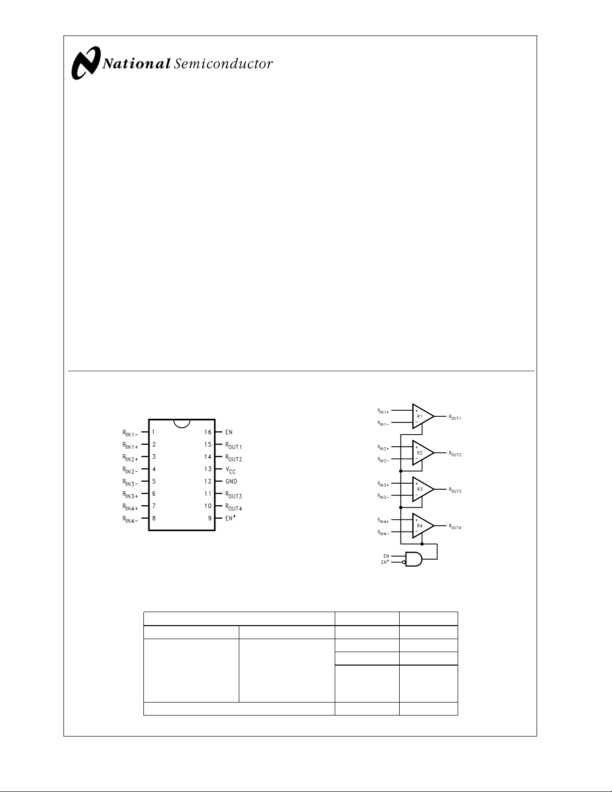
Connection Diagram
Dual-in-Line
Features
>
n
400 Mbps (200 MHz) switching rates
n Flow-through pinout simplifies PCB layout
n 150 ps channel-to-channel skew (typical)
n 100 ps differential skew (typical)
n 2.7 ns maximum propagation delay
n 3.3V power supply design
n High impedance LVDS inputs on power down
n Low Power design (40mW 3.3V static)
n Interoperable with existing 5V LVDS drivers
n Accepts small swing (350 mV typical) differential signal
levels
n Supports open, short and terminated input fail-safe
n 0V to −100mV threshold region
n Conforms to ANSI/TIA/EIA-644 Standard
n Industrial temperature operating range (-40˚C to +85˚C)
n Available in SOIC and TSSOP package
Functional Diagram
Order Number DS90LV048ATM, DS90LV048ATMTC
See NS Package Number M16A, MTC16
10088801
10088802
Truth Table
ENABLES INPUTS OUTPUT
EN EN* R
H L or Open VID≥ 0V H
All other combinations of ENABLE inputs X Z
TRI-STATE®is a registered trademark of National Semiconductor Corporation.
© 2001 National Semiconductor Corporation DS100888 www.national.com
IN+−RIN−
V
≤ −0.1V L
ID
Full Fail-safe
OPEN/SHORT
or Terminated
R
OUT
H
Page 2
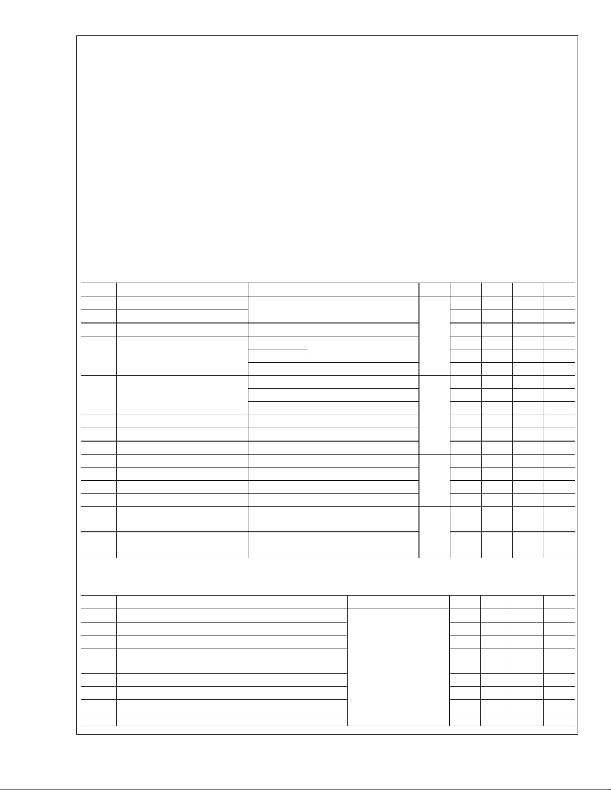
Absolute Maximum Ratings (Note 1)
If Military/Aerospace specified devices are required,
please contact theNational Semiconductor Sales Office/
Distributors for availability and specifications.
DS90LV048A
Supply Voltage (V
Input Voltage (R
Enable Input Voltage (EN, EN*) −0.3V to (V
Output Voltage (R
Maximum Package Power Dissipation +25˚C
M Package 1025 mW
MTC Package 866 mW
Derate M Package 8.2 mW/˚C above +25˚C
Derate MTC Package 6.9 mW/˚C above +25˚C
Storage Temperature Range −65˚C to +150˚C
) −0.3V to +4V
CC
IN+,RIN−
) −0.3V to 3.9V
) −0.3V to (VCC+ 0.3V)
OUT
CC
+ 0.3V)
(4 sec.) +260˚C
Maximum Junction
Temperature +150˚C
ESD Rating (Note 10)
(HBM, 1.5 kΩ, 100 pF) ≥ 10 kV
(EIAJ, 0 Ω, 200 pF) ≥ 1200 V
Recommended Operating
Conditions
Min Typ Max Units
Supply Voltage (V
) +3.0 +3.3 +3.6 V
CC
Receiver Input Voltage GND +3.0 V
Operating Free Air
Temperature (T
) −40 25 +85 ˚C
A
Lead Temperature Range Soldering
Electrical Characteristics
Over Supply Voltage and Operating Temperature ranges, unless otherwise specified. (Notes 2, 3)
Symbol Parameter Conditions Pin Min Typ Max Units
V
TH
V
TL
VCMR Common-Mode Voltage Range VID = 200mV pk to pk (Note 5) 0.1 2.3 V
I
IN
V
OH
V
OL
I
OS
I
OZ
V
IH
V
IL
I
I
V
CL
I
CC
I
CCZ
Differential Input High Threshold VCM= +1.2V, 0.05V, 2.95V (Note 13) R
Differential Input Low Threshold R
Input Current VIN= +2.8V VCC= 3.6V or 0V −10
V
= 0V −10
IN
V
= +3.6V VCC= 0V -20
IN
Output High Voltage IOH= −0.4 mA, VID= +200 mV R
I
= −0.4 mA, Input terminated 2.7 3.3 V
OH
I
= −0.4 mA, Input shorted 2.7 3.3 V
OH
, −35 0 mV
IN+
−100 −35 mV
IN−
±
5 +10 µA
±
1 +10 µA
±
1 +20 µA
2.7 3.3 V
OUT
Output Low Voltage IOL= 2 mA, VID= −200 mV 0.05 0.25 V
Output Short Circuit Current Enabled, V
Output TRI-STATE Current Disabled, V
Input High Voltage EN,
Input Low Voltage GND 0.8 V
Input Current VIN=0VorVCC, Other Input = VCCor GND −10
= 0V (Note 11) −15 −47 −100 mA
OUT
OUT
=0VorV
CC
−10
±
1 +10 µA
2.0 V
EN*
±
5 +10 µA
CC
Input Clamp Voltage ICL= −18 mA −1.5 −0.8 V
No Load Supply Current
EN=VCC, Inputs Open V
CC
915mA
Receivers Enabled
No Load Supply Current EN = GND, Inputs Open 1 5 mA
Receivers Disabled
V
Switching Characteristics
Over Supply Voltage and Operating Temperature ranges, unless otherwise specified. (Notes 3, 4, 7, 8)
Symbol Parameter Conditions Min Typ Max Units
t
PHLD
t
PLHD
t
SKD1
t
SKD2
Differential Propagation Delay High to Low CL= 15 pF 1.2 2.0 2.7 ns
Differential Propagation Delay Low to High VID= 200 mV 1.2 1.9 2.7 ns
Differential Pulse Skew |t
PHLD−tPLHD
Differential Channel-to-Channel Skew; same device
| (Note 6) (
Figure 1
and
Figure 2
) 0 0.1 0.4 ns
0 0.15 0.5 ns
(Note 7)
t
SKD3
t
SKD4
t
TLH
t
THL
www.national.com 2
Differential Part to Part Skew (Note 8) 1.0 ns
Differential Part to Part Skew (Note 9) 1.5 ns
Rise Time 0.5 1.0 ns
Fall Time 0.35 1.0 ns
Page 3
Over Supply Voltage and Operating Temperature ranges, unless otherwise specified. (Notes 3, 4, 7, 8)
Switching Characteristics (Continued)
Symbol Parameter Conditions Min Typ Max Units
t
PHZ
t
PLZ
t
PZH
t
PZL
f
MAX
Disable Time High to Z RL=2kΩ 814ns
Disable Time Low to Z CL=15pF 8 14 ns
Enable Time Z to High (
Figure 3
and
Figure 4
) 9 14 ns
Enable Time Z to Low 914ns
Maximum Operating Frequency (Note 14) All Channels Switching 200 250 MHz
Note 1: “Absolute Maximum Ratings” are those values beyond which the safety of the device cannot be guaranteed. They are not meant to imply that the devices
should be operated at these limits. The table of “Electrical Characteristics” specifies conditions of device operation.
Note 2: Current into device pins is defined as positive. Current out of device pins is defined as negative. All voltages are referenced to ground unless otherwise
specified.
Note 3: All typicals are given for: V
Note 4: Generator waveform for all tests unless otherwise specified:f=1MHz, Z
Note 5: The VCMR range is reduced for larger VID.Example:if VID = 400mV,the VCMR is 0.2V to 2.2V.The fail-safe condition with inputs shorted is not supported
over the common-mode range of 0V to 2.4V, but is supported only with inputs shorted and no external common-mode voltage applied. A VID up to V
be applied to the R
from 200mV to 400mV. Skew specifications apply for 200mV ≤ VID ≤ 800mV over the common-mode range .
Note 6: t
Note 7: t
any event on the inputs.
Note 8: t
and within 5˚C of each other within the operating temperature range.
Note 9: t
operating temperature and voltage ranges, and across process distribution. t
Note 10: ESD Rating:HBM (1.5 kΩ, 100 pF) ≥ 10kV
EIAJ (0Ω, 200 pF) ≥ 1200V
Note 11: Output short circuit current (I
exceed maximum junction temperature specification.
Note 12: C
Note 13: V
AC specifications, the common voltage range is 0.1V to 2.3V
Note 14: f
(max 0.4V), VOH(min 2.7V), Load = 15 pF (stray plus probes).
V
OL
is the magnitude difference in differential propagation delay time between the positive going edge and the negative going edge of the same channel
SKD1
, Channel-to-Channel Skew is defined as the difference between the propagation delay of one channel and that of the others on the same chip with
SKD2
, part to part skew, is the differential channel-to-channel skew of any event between devices. This specification applies to devices at the same VCC,
SKD3
, part to part skew, is the differential channel-to-channel skew of any event between devices. This specification applies to devices over recommended
SKD4
includes probe and jig capacitance.
L
is always higher than R
CC
generator input conditions: tr=t
MAX
inputs with the Common-Mode voltage set to VCC/2. Propagation delay and Differential Pulse skew decrease when VID is increased
IN+/RIN−
= +3.3V, TA= +25˚C.
CC
) is specified as magnitude only, minus sign indicates direction only. Only one output should be shorted at a time, do not
OS
and R
IN+
voltage. R
IN−
<
1 ns (0% to 100%), 50% duty cycle, differential (1.05V to 1.35V peak to peak). Output criteria: 60/40% dutycycle,
f
IN−
and R
are allowed to have a voltage range −0.2V to VCC− VID/2. However,to be compliant with
IN+
=50Ω,trand tf(0% to 100%) ≤ 3 ns for RIN.
O
is defined as |Max−Min| differential propagation delay.
SKD4
−0Vmay
CC
DS90LV048A
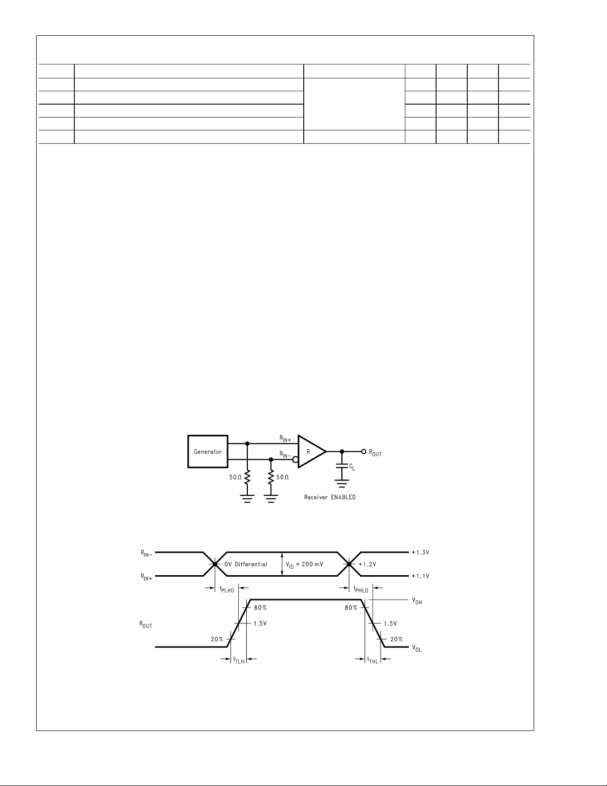
Parameter Measurement Information
FIGURE 1. Receiver Propagation Delay and Transition Time Test Circuit
FIGURE 2. Receiver Propagation Delay and Transition Time Waveforms
10088803
10088804
www.national.com3
Page 4
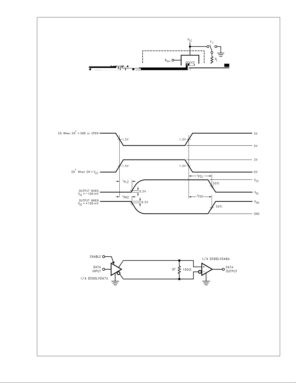
Parameter Measurement Information (Continued)
DS90LV048A
CLincludes load and test jig capacitance.
S
for t
and t
1=VCC
S
= GND for t
1
PZL
PZH
PLZ
and t
measurements.
measurements.
PHZ
10088805
FIGURE 3. Receiver TRI-STATE Delay Test Circuit
10088806
FIGURE 4. Receiver TRI-STATE Delay Waveforms
Typical Application
Balanced System
FIGURE 5. Point-to-Point Application
Applications Information
General application guidelines and hints for LVDS drivers
and receivers may be found in the following application
notes: LVDS Owner’s Manual (lit #550062-002), AN-808,
AN-977, AN-971, AN-916, AN-805, AN-903. The latest applications material is available on the web at:
www.national.com/lvds.
LVDSdriversand receivers are intendedto be primarily used
in an uncomplicated point-to-point configuration as is shown
www.national.com 4
10088807
in
Figure 5
. This configuration provides a clean signaling
environment for the fast edge rates of the drivers. The receiver is connected to the driver through a balanced media
which may be a standard twisted pair cable, a parallel pair
cable, or simply PCB traces. Typically, the characteristic
impedance of the media is in the range of 100Ω. A termination resistor of 100Ω (selected to match the media), and is
located as close to the receiver input pins as possible. The
Page 5

Applications Information (Continued)
termination resistor converts thedriver output (current mode)
into a voltage that is detected by the receiver.Other configurations are possible such as a multi-receiver configuration,
but the effects of a mid-stream connector(s), cable stub(s),
and other impedance discontinuities as well as ground shifting, noise margin limits, and total termination loading must
be taken into account.
The DS90LV048A differential line receiver is capable of detecting signals as low as 100mV, over a
range centered around +1.2V. This is related to the driver
offset voltage which is typically +1.2V. The driven signal is
centered around this voltage and may shift
center point. The
potential difference between the driver’s ground reference
and the receiver’s ground reference, the common-mode effects of coupled noise, or a combination of the two. The AC
parameters of both receiver input pins are optimized for a
recommended operating input voltage range of 0V to +2.4V
(measured from each pin to ground). The device will operate
for receiver input voltages up to V
turn on the ESD protection circuitry which will clamp the bus
voltages.
The DS90LV048A has a flow-through pinout that allows for
easy PCB layout. The LVDS signals on one side of the
device easily allows for matching electrical lengths of the
differential pair trace lines between the driver and the receiver as well as allowing the trace lines to be close together
to couple noise as common-mode. Noise isolation is
achieved with the LVDS signals on one side of the device
and the TTL signals on the other side.
Power Decoupling Recommendations:
Bypass capacitors must be used on power pins. Use high
frequency ceramic (surface mount is recommended) 0.1µF
and 0.001µF capacitors in parallel at the power supply pin
with the smallest value capacitor closest to the device supply
pin. Additional scattered capacitors over the printed circuit
board will improve decoupling. Multiple vias should be used
to connect the decoupling capacitors to the power planes. A
10µF (35V) or greater solid tantalum capacitor should be
connected at the power entry point on the printed circuit
board between the supply and ground.
PC Board considerations:
Use at least 4 PCB layers (top to bottom); LVDS signals,
ground, power, TTL signals.
Isolate TTL signals from LVDS signals, otherwise the TTL
may couple onto the LVDS lines. It is best to put TTL and
LVDS signals on different layers which are isolated by a
power/ground plane(s)
Keep drivers and receivers as close to the (LVDS port side)
connectors as possible.
Differential Traces:
Use controlled impedance traces which match the differen-
±
1V shifting may be the result of a ground
±
1V common-mode
±
1V around this
, but exceeding VCCwill
CC
Page 6

Applications Information (Continued)
gin (+25mV −(−35mV)). With the enhanced threshold region
of −100mV to 0V, this small external fail-safe biasing of
+25mV (with respect to 0V) gives a DNM of a comfortable
DS90LV048A
60mV. With the standard threshold region of
FIGURE 6. VTC of the DS90LV048A LVDS Receiver
Fail-Safe Feature:
The LVDS receiver is a high gain, high speed device that
amplifies a small differential signal (20mV) to CMOS logic
levels. Due to the high gain and tight threshold of the receiver,care should betaken to preventnoise from appearing
as a valid signal.
The receiver’s internal fail-safe circuitry is designed to
source/sink a small amount of current, providing fail-safe
protection (a stable known state of HIGH output voltage) for
floating, terminated or shorted receiver inputs.
1. Open Input Pins. The DS90LV048Ais a quad receiver
device, and if an application requires only 1, 2 or 3
receivers, the unused channel(s) inputs should be left
OPEN. Do not tie unused receiver inputs to ground or
any other voltages. The input is biased by internal high
value pull up and pull down resistors to set the output to
a HIGH state. This internal circuitry will guarantee a
HIGH, stable output state for open inputs.
2. Terminated Input. If the driver is disconnected (cable
unplugged), or if the driver is in a TRI-STATE or poweroff condition, the receiver output will again be in a HIGH
state, even with the end of cable 100Ω termination resistor across the input pins. The unplugged cable can
become a floating antenna which can pick up noise. If
the cable picks up more than 10mV of differential noise,
the receiver may see the noise as a valid signal and
switch. To insure that any noise is seen as commonmode and not differential, a balanced interconnect
should be used. Twisted pair cable will offer better balance than flat ribbon cable.
3. Shorted Inputs. If a fault condition occurs that shorts
the receiver inputs together, thus resulting in a 0V differential input voltage, the receiver output will remain in a
HIGH state. Shorted input fail-safe is not supported
across the common-mode range of the device (GND to
2.4V). It is only supported with inputs shorted and no
external common-mode voltage applied.
±
100mV, the
external fail-safe biasing would need to be +25mV with
respect to +100mV or +125mV, giving a DNM of 160mV
which is stronger fail-safe biasing than is necessary for the
DS90LV048A. If more DNM is required, then a stronger
fail-safe bias point can be set by changing resistor values.
10088830
External lower value pull up and pull down resistors (for a
stronger bias) may be used to boost fail-safe in the presence
of higher noise levels. The pull up and pull down resistors
should be in the 5kΩ to 15kΩ range to minimize loading and
waveform distortion to the driver. The common-mode bias
point should be set to approximately 1.2V (less than 1.75V)
to be compatible with the internal circuitry.
Additional information on fail-safe biasing of LVDS devices
may be found in AN-1194.
Pin Descriptions
Pin No. Name Description
2, 3, 6, 7 R
1, 4, 5, 8 R
10, 11, 14, R
15
16 EN Receiver enable pin: When EN is
9 EN* Receiver enable pin: When EN* is
13 V
12 GND Ground pin
Non-inverting receiver input pin
IN+
Inverting receiver input pin
IN−
Receiver output pin
OUT
low, the receiver is disabled.
When EN is high and EN* is low
or open, the receiver is enabled. If
both EN and EN* are open circuit,
then the receiver is disabled.
high, the receiver is disabled.
When EN* is low or open and EN
is high, the receiver is enabled. If
both EN and EN* are open circuit,
then the receiver is disabled.
Power supply pin, +3.3V±0.3V
CC
Ordering Information
Operating Package Type/ Order Number
Temperature Number
−40˚C to +85˚C SOP/M16A DS90LV048ATM
−40˚C to +85˚C TSSOP/MTC16 DS90LV048ATMTC
www.national.com 6
Page 7

Typical Performance Curves
DS90LV048A
Output High Voltage vs
Power Supply Voltage
10088812
Output Short Circuit Current vs
Power Supply Voltage
Output Low Voltage vs
Power Supply Voltage
10088813
Output TRI-STATE Current vs
Power Supply Voltage
10088814
Differential Transition Voltage vs
Power Supply Voltage
10088816
10088815
Power Supply Current
vs Frequency
10088817
www.national.com7
Page 8

Typical Performance Curves (Continued)
DS90LV048A
Power Supply Current vs
Ambient Temperature
10088818
Differential Propagation Delay vs
Ambient Temperature
Differential Propagation Delay vs
Power Supply Voltage
10088819
Differential Propagation Delay vs
Differential Input Voltage
10088820
Differential Propagation Delay vs
Common-Mode Voltage
10088822
www.national.com 8
10088821
Differential Skew vs
Power Supply Voltage
10088823
Page 9

Typical Performance Curves (Continued)
DS90LV048A
Differential Skew vs
Ambient Temperature
Transition Time vs
Ambient Temperature
10088824
Transition Time vs
Power Supply Voltage
10088825
10088826
www.national.com9
Page 10

Physical Dimensions inches (millimeters)
unless otherwise noted
DS90LV048A
16-Lead (0.150" Wide) Molded Small Outline Package, JEDEC
Order Number DS90LV048ATM
NS Package Number M16A
www.national.com 10
Page 11

Physical Dimensions inches (millimeters) unless otherwise noted (Continued)
DS90LV048A 3V LVDS Quad CMOS Differential Line Receiver
16-Lead (0.100" Wide) Molded Thin Shrink Small Outline Package, JEDEC
Order Number DS90LV048ATMTC
NS Package Number MTC16
LIFE SUPPORT POLICY
NATIONAL’S PRODUCTS ARE NOT AUTHORIZED FOR USE AS CRITICAL COMPONENTS IN LIFE SUPPORT
DEVICES OR SYSTEMS WITHOUT THE EXPRESS WRITTEN APPROVAL OF THE PRESIDENT AND GENERAL
COUNSEL OF NATIONAL SEMICONDUCTOR CORPORATION. As used herein:
1. Life support devices or systems are devices or
systems which, (a) are intended for surgical implant
into the body, or (b) support or sustain life, and
whose failure to perform when properly used in
accordance with instructions for use provided in the
2. A critical component is any component of a life
support device or system whose failure to perform
can be reasonably expected to cause the failure of
the life support device or system, or to affect its
safety or effectiveness.
labeling, can be reasonably expected to result in a
significant injury to the user.
National Semiconductor
Corporation
Americas
Email: support@nsc.com
www.national.com
National does not assume any responsibility for use of any circuitry described, no circuit patent licenses are implied and National reserves the right at any time without notice to change said circuitry and specifications.
National Semiconductor
Europe
Fax: +49 (0) 180-530 85 86
Email: europe.support@nsc.com
Deutsch Tel: +49 (0) 69 9508 6208
English Tel: +44 (0) 870 24 0 2171
Français Tel: +33 (0) 1 41 91 8790
National Semiconductor
Asia Pacific Customer
Response Group
Tel: 65-2544466
Fax: 65-2504466
Email: ap.support@nsc.com
National Semiconductor
Japan Ltd.
Tel: 81-3-5639-7560
Fax: 81-3-5639-7507
 Loading...