

Page 1
DS90LV032A
3V LVDS Quad CMOS Differential Line Receiver
DS90LV032A 3V LVDS Quad CMOS Differential Line Receiver
July 1999
General Description
The DS90LV032Ais a quad CMOS differential line receiver
designed for applications requiring ultra low power dissipation and high data rates. The device is designed to support
data rates in excess of 400 Mbps (200 MHz) utilizing Low
Voltage Differential Signaling (LVDS) technology.
The DS90LV032Aaccepts low voltage (350 mV typical) differential input signals and translates them to 3V CMOS output levels. The receiver supports a TRI-STATE
may be used to multiplex outputs. The receiver also supports
open, shorted and terminated (100Ω) input Fail-safe. The receiver output will be HIGH for all fail-safe conditions.
The DS90LV032A and companion LVDS line driver (eg.
DS90LV031A) provide a new alternative to high power
PECL/ECL devices for high speed point-to-point interface
applications.
®
function that
Features
>
n
400 Mbps (200 MHz) switching rates
n 0.1 ns channel-to-channel skew (typical)
n 0.1 ns differential skew (typical)
n 3.3 ns maximum propagation delay
n 3.3V power supply design
n Power down high impedance on LVDS inputs
n Low Power design (40mW 3.3V static)
n Interoperable with existing 5V LVDS networks
n Accepts small swing (350 mV typical) VID
n Supports open, short and terminated input fail-safe
n Compatible with ANSI/TIA/EIA-644
n Industrial temp. operating range (-40˚C to +85˚C)
n Available in SOIC and TSSOP Packaging
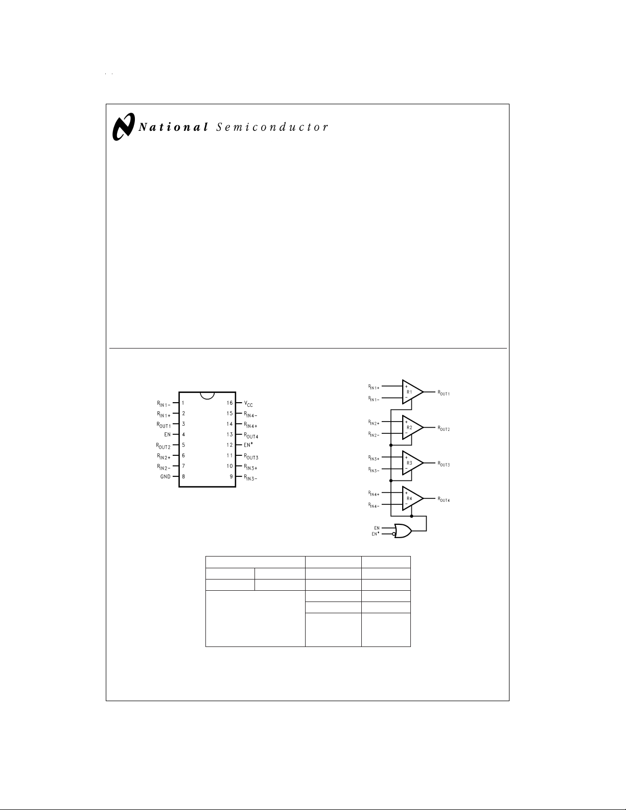
Connection Diagram Functional Diagram
Dual-in-Line
DS100067-1
Order Number DS90LV032ATM
See NS Package Number M16A or MTC16
or DS90LV032ATMTC
DS100067-2
ENABLES INPUTS OUTPUT
EN EN* R
LH X Z
All other combinations V
of ENABLE inputs V
© 1999 National Semiconductor Corporation DS100067 www.national.com
IN+−RIN−
≥ 0.1V H
ID
≤ −0.1V L
ID
Full Fail-safe
OPEN/SHORT H
or Terminated
R
OUT
Page 2

Absolute Maximum Ratings (Note 1)
If Military/Aerospace specified devices are required,
please contact the National Semiconductor Sales Office/
Distributors for availability and specifications.
Supply Voltage (V
Input Voltage (R
Enable Input Voltage (EN, EN*) −0.3V to (V
Output Voltage (R
Maximum Package Power Dissipation +25˚C
M Package 1025 mW
MTC Package 866 mW
Derate M Package 8.2 mW/˚C above +25˚C
Derate MTC Package 6.9 mW/˚C above +25˚C
Storage Temperature Range −65˚C to +150˚C
) −0.3V to +4V
CC
) −0.3V to +3.9V
IN+,RIN−
) −0.3V to (VCC+ 0.3V)
OUT
CC
+ 0.3V)
(Soldering 4 sec.) +260˚C
Maximum Junction Temperature +150˚C
ESD Rating (Note 10)
(HBM 1.5 kΩ, 100 pF) ≥ 4.5 kV
(EIAJ 0 Ω, 200 pF) ≥ 250 V
Recommended Operating
Conditions
Supply Voltage (V
) +3.0 +3.3 +3.6 V
CC
Receiver Input Voltage GND +3.0 V
Operating Free Air
Temperature (T
) −40 25 +85 ˚C
A
Min Typ Max Units
Lead Temperature Range
Electrical Characteristics
Over Supply Voltage and Operating Temperature ranges, unless otherwise specified. (Note 2)
Symbol Parameter Conditions Pin Min Typ Max Units
V
V
Differential Input High Threshold VCM= +1.2V
TH
Differential Input Low Threshold −100 −20 mV
TL
(Note 13)
VCMR Common-Mode Voltage Range VID=200 mV peak to peak (Note 5) 0.1 2.3 V
I
V
V
I
I
V
V
I
V
I
Input Current VIN= +2.8V VCC= 3.6V or 0V −10
IN
Output High Voltage IOH= −0.4 mA, VID= +200 mV R
OH
Output Low Voltage IOL= 2 mA, VID= −200 mV 0.1 0.25 V
OL
Output Short Circuit Current Enabled, V
OS
Output TRI-STATE Current Disabled, V
OZ
Input High Voltage EN,
IH
Input Low Voltage GND 0.8 V
IL
Input Current VIN=0VorVCC, Other Input = VCCor
I
Input Clamp Voltage ICL= −18 mA −1.5 −0.8 V
CL
No Load Supply Current EN, EN* = VCCor GND, Inputs Open V
CC
V
= 0V −10
IN
V
= +3.6V VCC= 0V -20 +20 µA
IN
I
= −0.4 mA, Input terminated 2.7 3.0 V
OH
I
= −0.4 mA, Input shorted 2.7 3.0 V
OH
= 0V (Note 11) −15 −48 −120 mA
OUT
=0VorV
OUT
CC
GND
Receivers Enabled EN, EN* = 2.4V or 0.5V, Inputs Open 10 15 mA
I
No Load Supply Current
CCZ
Receivers Disabled
EN = GND, EN* = VCC, Inputs Open 3 5 mA
R
,
IN+
R
IN−
2.7 3.0 V
OUT
−10
2.0 V
EN*
−10
CC
+20 +100 mV
±
1 +10 µA
±
1 +10 µA
±
1 +10 µA
CC
±
1 +10 µA
10 15 mA
V
Switching Characteristics
Over Supply Voltage and Operating Temperature ranges, unless otherwise specified. (Notes 3, 4, 7, 8)
Symbol Parameter Conditions Min Typ Max Units
t
t
t
t
t
t
t
t
www.national.com 2
Differential Propagation Delay High to Low CL= 10 pF 1.8 3.3 ns
PHLD
Differential Propagation Delay Low to High VID= 200 mV 1.8 3.3 ns
PLHD
Differential Pulse Skew |t
SKD1
Differential Channel-to-Channel Skew-same device
SKD2
(Note 7)
Differential Part to Part Skew (Note 8) 1.0 ns
SKD3
Differential Part to Part Skew (Note 9) 1.5 ns
SKD4
Rise Time 0.35 1.2 ns
TLH
Fall Time 0.35 1.2 ns
THL
PHLD−tPLHD
| (Note 6) (
Figure 1
and
Figure 2
) 0 0.1 0.35 ns
0 0.1 0.5 ns
Page 3
Switching Characteristics (Continued)
Page 4

Parameter Measurement Information (Continued)
CLincludes load and test jig capacitance.
for t
, and t
S
1=VCC
= GND for t
S
1
PZL
PZH
and t
measurements.
PLZ
measurements.
PHZ
Typical Application
DS100067-5
FIGURE 3. Receiver TRI-STATE Delay Test Circuit
DS100067-6
FIGURE 4. Receiver TRI-STATE Delay Waveforms
Balanced System
FIGURE 5. Point-to-Point Application
Applications Information
General application guidelines and hints for LVDS drivers
and receivers may be found in the following application
notes: LVDS Owner’s Manual (lit #550062-001), AN808,
AN1035, AN977, AN971, AN916, AN805, AN903.
LVDSdriversand receivers are intended to be primarily used
in an uncomplicated point-to-point configuration as is shown
in
Figure 5
vironment for the fast edge rates of the drivers . The receiver
is connected to the driver through a balanced media which
may be a standard twisted pair cable, a parallel pair cable, or
simply PCB traces. Typically the characteristic impedance of
www.national.com 4
. This configuration provides a clean signaling en-
DS100067-7
the media is in the range of 100Ω. A termination resistor of
100Ω should be selected to match the media, and is located
as close to the receiver input pins as possible. The termination resistor converts the driver output (current mode) into a
voltage that is detected by the receiver.Other configurations
are possible such as a multi-receiver configuration, but the
effects of a mid-stream connector(s), cable stub(s), and
other impedance discontinuities as well as ground shifting,
noise margin limits, and total termination loading must be
taken into account.
Page 5

Applications Information (Continued)
The DS90LV032Adifferential line receiver is capable of detecting signals as low as 100 mV, over a
range centered around +1.2V. This is related to the driver offset voltage which is typically +1.2V.The driven signal is centered around this voltage and may shift
ter point. The
potential difference between the driver’s ground reference
and the receiver’s ground reference, the common-mode effects of coupled noise, or a combination of the two. Both receiver input pins have a recommended operating input voltage range of 0V to +2.4V (measured from each pin to
ground), exceeding these limits may turn on the ESD protection circuitry which will clamp the bus voltages.
Power Decoupling Recommendations:
Bypass capacitors must be used on power pins. High frequency ceramic (surface mount is recommended) 0.1µF in
parallel with 0.01µF, in parallel with 0.001µF at the power
supply pin as well as scattered capacitors over the printed
circuit board. Multiple vias should be used to connect the decoupling capacitors to the power planes A 10µF (35V) or
greater solid tantalum capacitor should be connected at the
power entry point on the printed circuit board.
PC Board considerations:
Use at least 4 PCB layers (top to bottom); LVDS signals,
ground, power, TTL signals.
Isolate TTL signals from LVDS signals, otherwise the TTL
may couple onto the LVDS lines. It is best to put TTL and
±
1V shifting may be the result of a ground
±
1V common-mode
±
1V around this cen-
Page 6

Applications Information (Continued)
3. Shorted Inputs. If a fault condition occurs that shorts
the receiver inputs together, thus resulting in a 0V differential input voltage, the receiver output will remain in a
HIGH state. Shorted input fail-safe is not supported
across the common-mode range of the device (GND to
2.4V). It is only supported with inputs shorted and no external common-mode voltage applied.
External lower value pull up and pull down resistors (for a
stronger bias) may be used to boost fail-safe in the presence
of higher noise levels. The pull up and pull down resistors
should be in the 5kΩ to 15kΩ range to minimize loading and
waveform distortion to the driver. The common-mode bias
point should be set to approximately 1.2V (less than 1.75V)
to be compatible with the internal circuitry.
The footprint of the DS90LV032Ais the same as the industry
standard 26LS32 Quad Differential (RS-422) Receiver.
Pin Descriptions
Pin
Name Description
No.
2, 6, R
Non-inverting receiver input pin
IN+
Pin
Name Description
No.
10, 14
1, 7, R
Inverting receiver input pin
IN−
9, 15
3, 5, R
Receiver output pin
OUT
11, 13
4 EN Active high enable pin, OR-ed with
EN*
12 EN* Active low enable pin, OR-ed with EN
16 V
Power supply pin, +3.3V±0.3V
CC
8 GND Ground pin
Ordering Information
Operating Package Type/ Order Number
Temperature Number
−40˚C to +85˚C SOP/M16A DS90LV032ATM
−40˚C to +85˚C TSSOP/MTC16 DS90LV032ATMTC
FIGURE 6. ICC vs Frequency, four channels switching
FIGURE 7. Typical Common-Mode Range variation with respect to amplitude of differential input
www.national.com 6
DS100067-8
DS100067-9
Page 7

Applications Information (Continued)
FIGURE 8. Typical Pulse Skew variation versus common-mode voltage
DS100067-10
DS100067-11
FIGURE 9. Variation in High to Low Propagation Delay versus VCM
DS100067-12
FIGURE 10. Variation in Low to High Propagation Delay versus VCM
www.national.com7
Page 8

Physical Dimensions inches (millimeters) unless otherwise noted
16-Lead (0.150" Wide) Molded Small Outline Package, JEDEC
Order Number DS90LV032ATM
NS Package Number M16A
www.national.com 8
Page 9

Physical Dimensions inches (millimeters) unless otherwise noted (Continued)
DS90LV032A 3V LVDS Quad CMOS Differential Line Receiver
16-Lead (0.100" Wide) Molded Thin Shrink Small Outline Package, JEDEC
Order Number DS90LV032ATMTC
NS Package Number MTC16
LIFE SUPPORT POLICY
NATIONAL’S PRODUCTS ARE NOT AUTHORIZED FOR USE AS CRITICAL COMPONENTS IN LIFE SUPPORT
DEVICES OR SYSTEMS WITHOUT THE EXPRESS WRITTEN APPROVAL OF THE PRESIDENT AND GENERAL
COUNSEL OF NATIONAL SEMICONDUCTOR CORPORATION. As used herein:
1. Life support devices or systems are devices or
systems which, (a) are intended for surgical implant
into the body, or (b) support or sustain life, and
whose failure to perform when properly used in
accordance with instructions for use provided in the
2. A critical component is any component of a life
support device or system whose failure to perform
can be reasonably expected to cause the failure of
the life support device or system, or to affect its
safety or effectiveness.
labeling, can be reasonably expected to result in a
significant injury to the user.
National Semiconductor
Corporation
Americas
Tel: 1-800-272-9959
Fax: 1-800-737-7018
Email: support@nsc.com
www.national.com
National does not assume any responsibility for use of any circuitry described, no circuit patent licenses are implied and National reserves the right at any time without notice to change said circuitry and specifications.
National Semiconductor
Europe
Fax: +49 (0) 1 80-530 85 86
Email: europe.support@nsc.com
Deutsch Tel: +49 (0) 1 80-530 85 85
English Tel: +49 (0) 1 80-532 78 32
Français Tel: +49 (0) 1 80-532 93 58
Italiano Tel: +49 (0) 1 80-534 16 80
National Semiconductor
Asia Pacific Customer
Response Group
Tel: 65-2544466
Fax: 65-2504466
Email: sea.support@nsc.com
National Semiconductor
Japan Ltd.
Tel: 81-3-5639-7560
Fax: 81-3-5639-7507
 Loading...