

Page 1
DS90LV027
LVDS Dual High Speed Differential Driver
General Description
The DS90LV027 is a dual LVDS driver device optimized for
high data rate and low power applications. The DS90LV027
is a current mode driver allowing power dissipation to remain
low even at high frequency. In addition, the short circuit fault
current is also minimized. The device is in a 8-lead small
Outline Package. The DS90LV027 has a flow-through design for easy PCB layout. The differential driver outputs provides low EMI with its low output swings typically 340 mV.
Perfect for high speed transfer of clock and data. Pair with
any of National’s LVDS receivers.
Features
n Ultra Low Power Dissipation
n Operating Range above 155 Mbps
n Flow-through pinout simplifies PCB layout
n Conforms to TIA/EIA-644 Standard
n 8-Lead SOIC Package Saves Space
n V
CM
±
1V center around 1.2V
n Low Differential Output Swing Typical 340 mV
n Power Off Protection (outputs in high impedance)
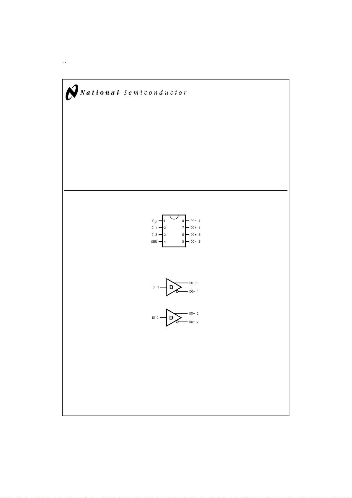
Connection Diagram
Functional Diagram
Dual-In-Line
DS100029-1
Order Number DS90LV027M
See NS Package Number M08A
DS100029-2
DS100029-3
June 1998
DS90LV027 LVDS Dual High Speed Differential Driver
© 1998 National Semiconductor Corporation DS100029 www.national.com
Page 2
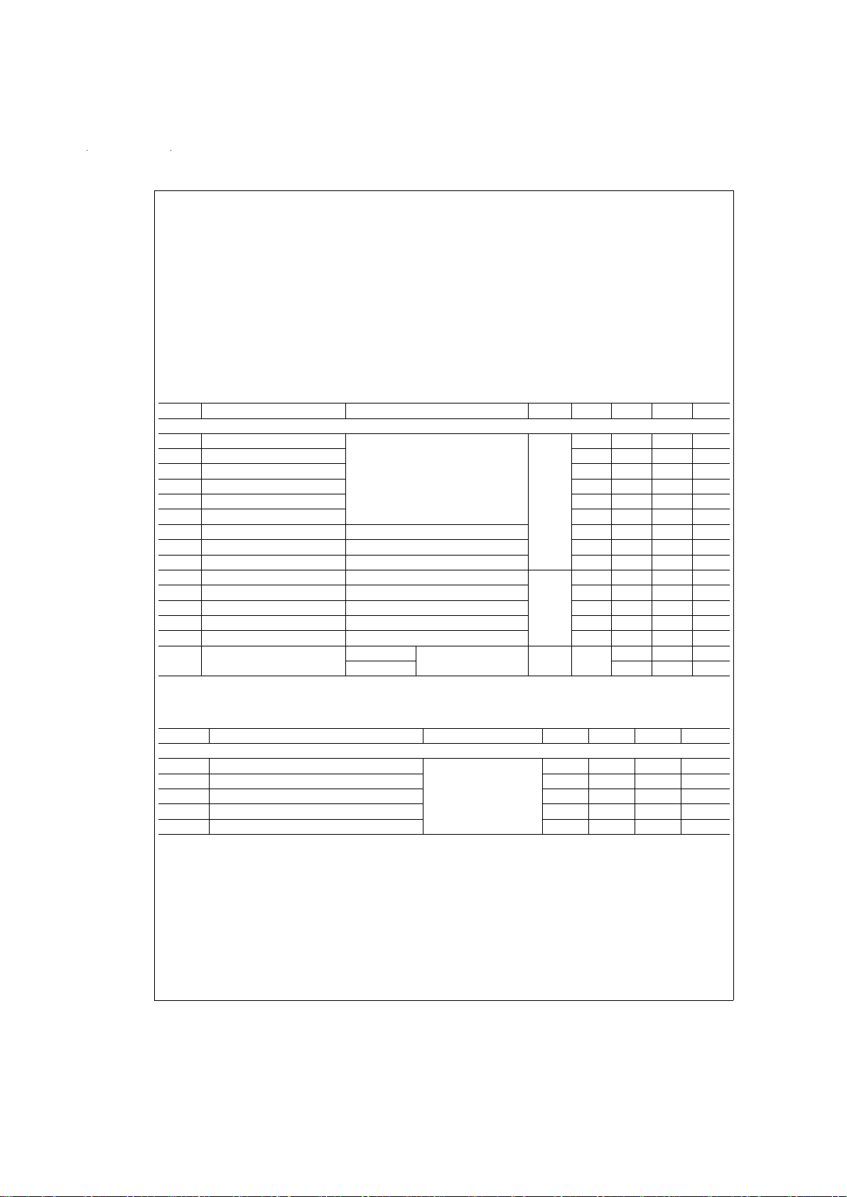
Absolute Maximum Ratings (Note 1)
If Military/Aerospace specified devices are required,
please contact the National Semiconductor Sales Office/
Distributors for availability and specifications.
Supply Voltage (V
CC
) −0.3V to +6V
Input Voltage (DI) −0.3V to (V
CC
+ 0.3V)
Output Voltage (DO
±
) −0.3V to +3.9V
Maximum Package Power Dissipation
@
+25˚C
M Package 1190 mW
Derate M Package 9.5 mW/˚C above +25˚C
Storage Temperature Range −65˚C to +150˚C
Lead Temperature Range
Soldering (4 sec.) +260˚C
ESD Rating (Note 4)
(HBM 1.5 kΩ, 100 pF) ≥ 4.5 kV
Recommended Operating
Conditions
Min Typ Max Units
Supply Voltage (V
CC
) 3.0 3.3 3.6 V
Temperature (T
A
) 0 25 70 ˚C
Electrical Characteristics
Over Supply Voltage and Operating Temperature ranges, unless otherwise specified. (Notes 2, 3, 7)
Symbol Parameter Conditions Pin Min Typ Max Units
DIFFERENTIAL DRIVER CHARACTERISTICS
V
OD
Output Differential Voltage R
L
=
100Ω
(Figure 1)
DO+,
DO−
250 340 450 mV
∆V
OD
VODMagnitude Change 0 10 35 mV
V
OH
Output High Voltage 1.43 1.6 V
V
OL
Output Low Voltage 0.9 1.09 V
V
OS
Offset Voltage 0.9 1.25 1.6 V
∆V
OS
Offset Magnitude Change 0 5 25 mV
I
OZD
TRI-STATE®Leakage V
OUT
=
V
CC
or GND 0
±
1
±
10 µA
I
OXD
Power-off Leakage V
OUT
=
3.6V or GND, V
CC
=
0V 0
±
1
±
10 µA
I
OSD
Output Short Circuit Current −4 −6 mA
V
IH
Input High Voltage DI 2.0 V
CC
V
V
IL
Input Low Voltage GND 0.8 V
I
IH
Input High Current V
IN
=
3.6V or 2.4V
±
1
±
10 µA
I
IL
Input Low Current V
IN
=
GND or 0.5V
±
1
±
10 µA
V
CL
Input Clamp Voltage I
CL
=
−18 mA −1.5 −0.8 V
I
CC
Power Supply Current No Load V
IN
=
V
CC
or GND V
CC
14mA
R
L
=
100Ω 811mA
Switching Characteristics
Over Supply Voltage and Operating Temperature Ranges, unless otherwise specified. (Notes 5, 6)
Symbol Parameter Conditions Min Typ Max Units
DIFFERENTIAL DRIVER CHARACTERISTICS
t
PHLD
Differential Propagation Delay High to Low R
L
=
100Ω,C
L
=
5pF
(
Figure 2
and
Figure 3
)
1.5 3.4 6 ns
t
PLHD
Differential Propagation Delay Low to High 1.5 3.5 6 ns
t
SKD
Differential Skew |t
PHLD−tPLHD
| 0 0.1 1.9 ns
t
TLH
Transition Low to High Time 0 1 3 ns
t
THL
Transition High to Low Time 0 1 3 ns
Note 1: “AbsoluteMaximum Ratings” are those values beyond which the safety of the device cannot be guaranteed. They are not meant to imply that the devices
should be operated at these limits. The table of “Electrical Characteristics” specifies conditions of device operation.
Note 2: Current into device pins is defined as positive. Current out of device pins is defined as negative. All voltages are referenced to ground except V
OD
.
Note 3: All typicals are given for: V
CC
=
+3.3V and T
A
=
+25˚C.
Note 4: ESD Rating: HBM (1.5 kΩ, 100 pF) ≥ 4.5 kV
Note 5: C
L
includes probe and fixture capacitance.
Note 6: Generator waveform for all tests unless otherwise specified: f=1 MHz, Z
O
=
50Ω,t
r
≤6 ns, tf≤ 6ns(10%-90%).
Note 7: The DS90LV027 is a current mode device and only function with datasheet specification when a resistive load is applied to the drivers outputs.
www.national.com 2
Page 3

Parameter Measurement Information
Application Information
Truth Table
Input/Output
DI DO+ DO−
LLH
HHL
DI
>
0.8V and DI<2.0V X X
H=Logic high level
L=Logic low level
X=indeterminant
TABLE 1. Device Pin Descriptions
Pin#Name Description
2, 3 DI TTL/CMOS driver input pins
6, 7 DO+ Non-inverting driver output pin
5, 8 DO− Inverting driver output pin
4 GND Ground pin
1V
CC
Positive power supply pin,
+3.3V
±
0.3V
DS100029-4
FIGURE 1. Differential Driver DC Test Circuit
DS100029-5
FIGURE 2. Differential Driver Propagation Delay and Transition Time Test Circuit
DS100029-6
FIGURE 3. Differential Driver Propagation Delay and Transition Time Waveforms
www.national.com3
Page 4

Physical Dimensions inches (millimeters) unless otherwise noted
LIFE SUPPORT POLICY
NATIONAL’S PRODUCTS ARE NOT AUTHORIZED FOR USE AS CRITICAL COMPONENTS IN LIFE SUPPORT DEVICES OR SYSTEMS WITHOUT THE EXPRESS WRITTEN APPROVAL OF THE PRESIDENT OF NATIONAL SEMICONDUCTOR CORPORATION. As used herein:
1. Life support devices or systems are devices or sys-
tems which, (a) are intended for surgical implant into
the body, or (b) support or sustain life, and whose failure to perform when properly used in accordance
with instructions for use provided in the labeling, can
be reasonably expected to result in a significant injury
to the user.
2. A critical component in any component of a life support
device or system whose failure to perform can be reasonably expected to cause the failure of the life support
device or system, or to affect its safety or effectiveness.
National Semiconductor
Corporation
Americas
Tel: 1-800-272-9959
Fax: 1-800-737-7018
Email: support@nsc.com
www.national.com
National Semiconductor
Europe
Fax: +49 (0) 1 80-530 85 86
Email: europe.support@nsc.com
Deutsch Tel: +49 (0) 1 80-530 85 85
English Tel: +49 (0) 1 80-532 78 32
Français Tel: +49 (0) 1 80-532 93 58
Italiano Tel: +49 (0) 1 80-534 16 80
National Semiconductor
Asia Pacific Customer
Response Group
Tel: 65-2544466
Fax: 65-2504466
Email: sea.support@nsc.com
National Semiconductor
Japan Ltd.
Tel: 81-3-5620-6175
Fax: 81-3-5620-6179
Order Number DS90LV027M
NS Package Number M08A
DS90LV027 LVDS Dual High Speed Differential Driver
National does not assume any responsibility for use of any circuitry described, no circuit patent licenses are implied and National reserves the right at any time without notice to change said circuitry and specifications.
 Loading...