

Page 1
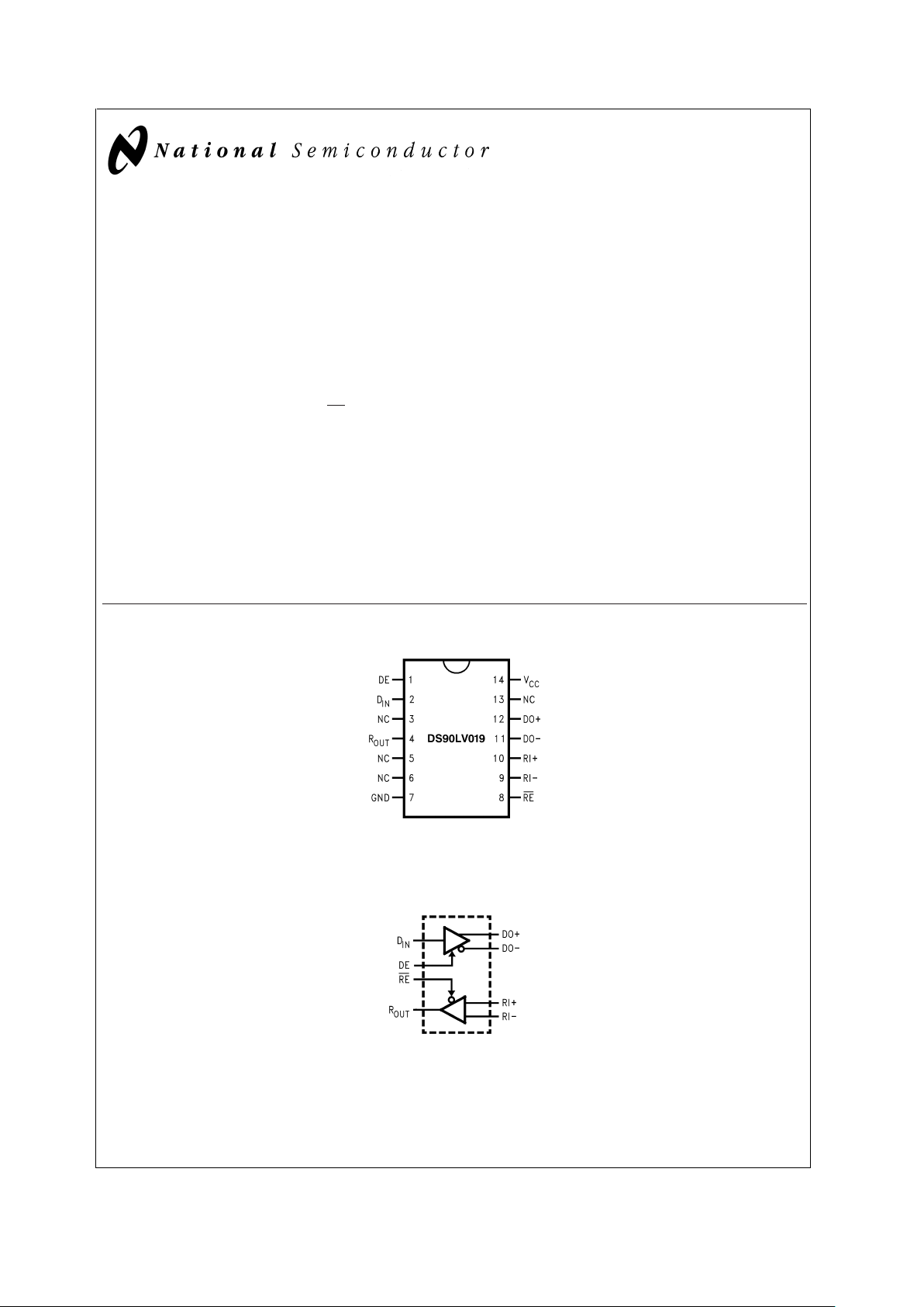
DS90LV019
3.3V or 5V LVDS Driver/Receiver
General Description
The DS90LV019 is a Driver/Receiver designed specifically
for the high speed low power point-to-point interconnect applications. The device operates from a single 3.3V or 5.0V
power supply and includes one differential line driver and
one receiver. The DS90LV019 features an independent
driver and receiver with TTL/CMOS compatibility (D
IN
and
R
OUT
). The logic interface provides maximum flexibility as 4
separate lines are provided (D
IN
, DE, RE, and R
OUT
). The
device also features a flow-through pin out which allows
easy PCB routing for short stubs between its pins and the
connector. The driver has 3.5 mA output loop current.
The driver translates between TTL levels (single-ended) to
Low Voltage DifferentialSignaling levels. This allows for high
speed operation, while consuming minimal power with reduced EMI. In addition, the differential signaling provides
common-mode noise rejection.
The receiver threshold is
±
100 mV over a±1V commonmode range and translates the low swing differential levels
to standard (TTL/CMOS) levels.
Features
n LVDS Signaling
n 3.3V or 5.0V operation
n Low power CMOS design
n Balanced Output Impedance
n Glitch free power up/down (Driver disabled)
n High Signaling Rate Capacity (above 100 Mbps)
n Ultra Low Power Dissipation
n
±
1V Common-Mode Range
n
±
100 mV Receiver Sensitivity
n Product offered in SOIC and TSSOP packages
n Flow-Through Pin Out
n Industrial Temperature Range Operation
Connection Diagram
Block Diagram
TRI-STATE®is a registered trademark of National Semiconductor Corporation.
DS100053-1
Order Number DS90LV019TM or DS90LV019TMTC
See NS Package Number M14A or MTC14
DS100053-2
August 2000
DS90LV019 3.3V or 5V LVDS Driver/Receiver
© 2000 National Semiconductor Corporation DS100053 www.national.com
Page 2
Absolute Maximum Ratings (Note 1)
If Military/Aerospace specified devices are required,
please contact the National Semiconductor Sales Office/
Distributors for availability and specifications.
Supply Voltage V
CC
6.0V
Enable Input Voltage (DE, RE)
−0.3V to (VCC+0.3V)
Driver Input Voltage (D
IN
) −0.3V to (VCC+ 0.3V)
Receiver Output Voltage
(R
OUT
) −0.3V to (VCC+ 0.3V)
Driver Output Voltage (DO
±
) −0.3V to +3.9V
Receiver Input Voltage (RI
±
) −0.3V to (VCC+ 0.3V)
Driver Short Circuit Current Continuous
ESD (Note 4)
(HBM, 1.5 kΩ, 100 pF)
>
2.0 kV
(EIAJ, 0 Ω, 200 pF)
>
200 V
Maximum Package Power Dissipation at 25˚C
SOIC 960 mW
Derate SOIC Package 7.7mW/˚C
TSSOP 790 mW
Derate TSSOP Package 6.3mW/˚C
Storage Temperature Range −65˚C to +150˚C
Lead Temperature
(Soldering, 4 sec.) 260˚C
Recommended Operating
Conditions
Min Max Units
Supply Voltage (V
CC
) or 3.0 3.6 V
Supply Voltage (V
CC
) 4.5 5.5 V
Receiver Input Voltage 0.0 2.4 V
Operating Free Air
Temperature T
A
−40 +85 ˚C
DC Electrical Characteristics
TA= −40˚C to +85˚C unless otherwise noted, VCC= 3.3±0.3V. (Notes 2, 3)
Symbol Parameter Conditions Pin Min Typ Max Units
DIFFERENTIAL DRIVER CHARACTERISTICS
V
OD
Output Differential Voltage RL= 100Ω (
Figure 1
) DO+,
DO−
250 350 450 mV
∆V
OD
VODMagnitude Change 660mV
V
OS
Offset Voltage 1 1.25 1.7 V
∆V
OS
Offset Magnitude Change 5 60 mV
I
OZD
TRI-STATE®Leakage V
OUT=VCC
or GND, DE = 0V −10
±
1 +10 µA
I
OXD
Power-Off Leakage V
OUT
= 3.6V or GND, VCC= 0V −10
±
1 +10 µA
I
OSD
Output Short Circuit Current V
OUT
= 0V, DE = V
CC
−10 −6 −4 mA
DIFFERENTIAL RECEIVER CHARACTERISTICS
V
OH
Voltage Output High VID = +100 mV IOH= −400 µA R
OUT
2.9 3.3 V
Inputs Open 2.9 3.3 V
V
OL
Voltage Output Low IOL= 2.0 mA, VID = −100 mV 0.1 0.4 V
I
OS
Output Short Circuit Current V
OUT
= 0V −75 −34 −20 mA
V
TH
Input Threshold High RI+,
RI−
+100 mV
V
TH
Input Threshold Low −100 mV
I
IN
Input Current VIN= +2.4V or 0V, VCC= 3.6V or
0V
−10
±
1 +10 µA
DEVICE CHARACTERISTICS
V
IH
Minimum Input High Voltage DIN,
DE, RE
2.0 V
CC
V
V
IL
Maximum Input Low Voltage GND 0.8 V
I
IH
Input High Current VIN=VCCor 2.4V
±
1
±
10 µA
I
IL
Input Low Current VIN= GND or 0.4V
±
1
±
10 µA
V
CL
Input Diode Clamp Voltage I
CLAMP
= −18 mA −1.5 −0.7 V
I
CCD
Power Supply Current DE = RE = V
CC
V
CC
9 12.5 mA
I
CCR
DE=RE=0V 4.5 7.0 mA
I
CCZ
DE = 0V, RE = V
CC
3.7 7.0 mA
I
CC
DE=VCC,RE=0V 15 20 mA
C
D output
Capacitance DO+,
DO−
5pF
C
R input
Capacitance RI+,
RI−
5pF
DS90LV019
www.national.com 2
Page 3
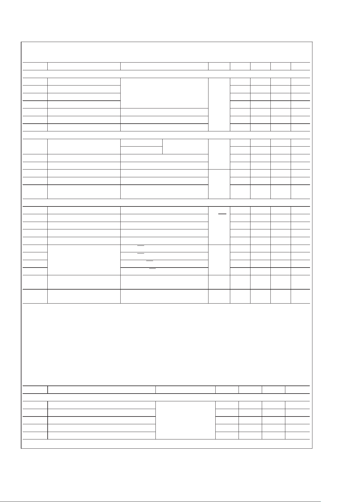
DC Electrical Characteristics
TA= −40˚C to +85˚C unless otherwise noted, VCC= 5.0±0.5V. (Notes 2, 3)
Symbol Parameter Conditions Pin Min Typ Max Units
DIFFERENTIAL DRIVER CHARACTERISTICS
V
OD
Output Differential Voltage RL= 100Ω (
Figure 1
) DO+,
DO−
250 360 450 mV
∆V
OD
VODMagnitude Change 660mV
V
OS
Offset Voltage 1 1.25 1.8 V
∆V
OS
Offset Magnitude Change 5 60 mV
I
OZD
TRI-STATE Leakage V
OUT=VCC
or GND, DE = 0V −10
±
1 +10 µA
I
OXD
Power-Off Leakage V
OUT
= 5.5V or GND, VCC= 0V −10
±
1 +10 µA
I
OSD
Output Short Circuit Current V
OUT
= 0V, DE = V
CC
−10 −6 −4 mA
DIFFERENTIAL RECEIVER CHARACTERISTICS
V
OH
Voltage High VID = +100 mV IOH= −400 µA R
OUT
4.3 5.0 V
Inputs Open 4.3 5.0 V
V
OL
Voltage Output Low IOL= 2.0 mA, VID = −100 mV 0.1 0.4 V
I
OS
Output Short Circuit Current V
OUT
= 0V −150 −75 −40 mA
V
TH
Input Threshold High RI+,
RI−
+100 mV
V
TH
Input Threshold Low −100 mV
I
IN
Input Current VIN= +2.4V or 0V, VCC= 5.5V or
0V
−15
±
1 +15 µA
DEVICE CHARACTERISTICS
V
IH
Minimum Input High Voltage DIN,
DE ,RE
2.0 V
CC
V
V
IL
Maximum Input Low Voltage GND 0.8 V
I
IH
Input High Current VIN=VCCor 2.4 V
±
1
±
10 µA
I
IL
Input Low Current VIN= GND or 0.4V
±
1
±
10 µA
V
CL
Input Diode Clamp Voltage I
CLAMP
= −18 mA −1.5 −0.8 V
I
CCD
Power Supply Current DE = RE = V
CC
V
CC
12 19 mA
I
CCR
DE=RE=0V 5.8 8 mA
I
CCZ
DE = 0V, RE = V
CC
4.5 8.5 mA
I
CC
DE=VCC,RE=0V 18 48 mA
C
D output
Capacitance DO+,
DO−
5pF
C
R input
Capacitance RI+,
RI−
5pF
Note 1: “Absolute Maximum Ratings” are these beyond which the safety of the device cannot be guaranteed. They are not meant to imply that the device should
be operated at these limits. The table of “Electrical Characteristics” provides conditions for actual device operation.
Note 2: All currents into device pins arepositive;allcurrentsout of device pins are negative. All voltages are referenced to device ground unless otherwise specified.
Note 3: All typicals are given for V
CC
= +3.3V or +5.0V and TA= +25˚C, unless otherwise stated.
Note 4: ESD Rating:
HBM (1.5 kΩ, 100 pF)
>
2.0 kV
EIAJ (0Ω, 200 pF)
>
200V.
Note 5: C
L
includes probe and fixture capacitance.
Note 6: Generator waveforms for all tests unless otherwise specified;f=1MHz, Z
O
=50Ω,tr=tf≤6.0 ns (0%–100%).
AC Electrical Characteristics
TA= −40˚C to +85˚C, VCC= 3.3V±0.3V. (Note 6)
Symbol Parameter Conditions Min Typ Max Units
DRIVER TIMING REQUIREMENTS
t
PHLD
Differential Propagation Delay High to Low RL= 100Ω,
C
L
=10pF
(
Figure 2
and
Figure 3
)
2.0 4.0 6.5 ns
t
PLHD
Differential Propagation Delay Low to High 1.0 5.6 7.0 ns
t
SKD
Differential Skew |t
PHLD−tPLHD
| 0.4 1.0 ns
t
TLH
Transition Time Low to High 0.2 0.7 3.0 ns
t
THL
Transition Time High to Low 0.2 0.8 3.0 ns
DS90LV019
www.national.com3
Page 4

AC Electrical Characteristics (Continued)
TA= −40˚C to +85˚C, VCC= 3.3V±0.3V. (Note 6)
Symbol Parameter Conditions Min Typ Max Units
DRIVER TIMING REQUIREMENTS
t
PHZ
Disable Time High to Z RL= 100Ω,
C
L
=10pF
(
Figure 4
and
Figure 5
)
1.5 4.0 8.0 ns
t
PLZ
Disable Time Low to Z 2.5 5.3 9.0 ns
t
PZH
Enable Time Z to High 4.0 6.0 8.0 ns
t
PZL
Enable Time Z to Low 3.5 6.0 8.0 ns
RECEIVER TIMING REQUIREMENTS
t
PHLD
Differential Propagation Delay High to Low CL=10pF,
VID = 200 mV
(
Figure 6
and
Figure 7
)
3.0 5.8 7.0 ns
t
PLHD
Differential Propagation Delay Low to High 3.0 5.6 9.0 ns
t
SKD
Differential Skew |t
PHLD−tPLHD
| 0.55 1.5 ns
t
r
Rise Time 0.15 2.0 3.0 ns
t
f
Fall Time 0.15 0.9 3.0 ns
t
PHZ
Disable Time High to Z RL= 500Ω,
C
L
=10pF
(
Figure 8
and
Figure 9
)
3.0 4.0 6.0 ns
t
PLZ
Disable Time Low to Z 3.0 4.5 6.0 ns
t
PZH
Enable Time Z to High 3.0 6.0 8.0 ns
t
PZL
Enable Time Z to Low 3.0 6.0 8.0 ns
AC Electrical Characteristics
TA= −40˚C to +85˚C, VCC= 5.0V±0.5V. (Note 6)
Symbol Parameter Conditions Min Typ Max Units
DRIVER TIMING REQUIREMENTS
t
PHLD
Differential Propagation Delay High to Low RL= 100Ω,
C
L
=10pF
(
Figure 2
and
Figure 3
)
2.0 3.3 6.0 ns
t
PLHD
Differential Propagation Delay Low to High 1.0 3.3 5.0 ns
t
SKD
Differential Skew |t
PHLD−tPLHD
| 0.6 1.0 ns
t
TLH
Transition Time Low to High 0.15 0.9 3.0 ns
t
THL
Transition Time High to Low 0.15 1.2 3.0 ns
t
PHZ
Disable Time High to Z RL= 100Ω,
C
L
=10pF
(
Figure 4
and
Figure 5
)
1.5 3.5 7.0 ns
t
PLZ
Disable Time Low to Z 3.0 5.2 9.0 ns
t
PZH
Enable Time Z to High 2.0 4.5 7.0 ns
t
PZL
Enable Time Z to Low 2.0 4.5 7.0 ns
RECEIVER TIMING REQUIREMENTS
t
PHLD
Differential Propagation Delay High to Low CL=10pF,
VID = 200 mV
(
Figure 6
and
Figure 7
)
3.0 6.0 8.0 ns
t
PLHD
Differential Propagation Delay Low to High 3.0 5.6 8.0 ns
t
SKD
Differential Skew |t
PHLD−tPLHD
| 0.7 1.6 ns
t
r
Rise Time 0.15 0.8 3.0 ns
t
f
Fall Time 0.15 0.8 3.0 ns
t
PHZ
Disable Time High to Z RL= 500Ω,
C
L
=10pF
(
Figure 8
and
Figure 9
)
3.0 3.5 4.5 ns
t
PLZ
Disable Time Low to Z 3.5 3.6 7.0 ns
t
PZH
Enable Time Z to High 3.0 5.0 7.0 ns
t
PZL
Enable Time Z to Low 3.0 5.0 7.0 ns
DS90LV019
www.national.com 4
Page 5

Test Circuits and Timing Waveforms
DS100053-3
FIGURE 1. Differential Driver DC Test Circuit
DS100053-4
FIGURE 2. Differential Driver Propagation Delay and Transition Test Circuit
DS100053-5
FIGURE 3. Differential Driver Propagation and Transition Time Waveforms
DS100053-6
FIGURE 4. Driver TRI-STATE Delay Test Circuit
DS90LV019
www.national.com5
Page 6

Test Circuits and Timing Waveforms (Continued)
DS100053-7
FIGURE 5. Driver TRI-STATE Delay Waveforms
DS100053-8
FIGURE 6. Receiver Propagation Delay and Transition Time Test Circuit
DS100053-9
FIGURE 7. Receiver Propagation Delay and Transition Time Waveforms
DS100053-10
FIGURE 8. Receiver TRI-STATE Delay Test Circuit
DS90LV019
www.national.com 6
Page 7

Test Circuits and Timing Waveforms (Continued)
Typical Application Diagram
Applications Information
The DS90LV019 has two control pins, which allows the device to operate as a driver, a receiver or both driver and a receiver at the same time. There are a few common practices
which should be implied when designing PCB for LVDS signaling. Recommended practices are:
•
Use at least 4 PCB board layer (LVDS signals, ground,
power and TTL signals).
•
Keep drivers and receivers as close to the (LVDS port
side) connector as possible.
•
Bypass each LVDS device and also use distributed bulk
capacitance. Surface mount capacitors placed close to
power and ground pins work best. Two or three multilayer ceramic (MLC) surface mount capacitors 0.1 µF,
and 0.01 µF in parallel should be used between each V
CC
and ground. The capacitors should be as close as possible to the V
CC
pin.
•
Use controlled impedance traces which match the differential impedance of your transmission medium (i.e.,
Cable) and termination resistor.
•
Use the termination resistor which best matches the differential impedance of your transmission line.
•
Isolate TTL signals from LVDS signals.
MEDIA (CABLE AND CONNECTOR) SELECTION:
•
Use controlled impedance media. The cables and connectors should have a matched differential impedance of
about 100Ω.
DS100053-11
FIGURE 9. Receiver TRI-STATE Delay Waveforms TRI-STATE Delay Waveforms
DS100053-13
FIGURE 10. Terminated Input Fail-Safe Circuit
DS100053-12
DS90LV019
www.national.com7
Page 8

Applications Information (Continued)
•
Balanced cables (e.g., twisted pair) are usually better
than unbalanced cables (ribbon cable, simple coax) for
noise reduction and signal quality.
•
For cable distances<0.5m, most cables can be made to
work effectively. For distances 0.5m ≤ d ≤ 10m, CAT 3
(category 3) twisted pair cable works well and is readily
available and relatively inexpensive. For distances
>
10m, and high data rates CAT 5 twisted pair is recom-
mended.
•
There are three Fail-Safe scenarios, open input pins,
shorted inputs pins and terminated input pins. The first
case is guaranteed for DS90LV019. A HIGH state on
R
OUT
pin can be achieved by using two external resistors
(one to V
CC
and one to GND) per
Figure 10
(Terminated
Input Fail-Safe Circuit). R1 and R2 should be R
T
to limit
the loading to the LVDS driver . R
T
is selected to match
the impedance of the cable.
TABLE 1. Functional Table
MODE SELECTED DE RE
DRIVER MODE H H
RECEIVER MODE L L
TRI-STATE MODE L H
FULL DUPLEX MODE H L
TABLE 2. Transmitter Mode
INPUTS OUTPUTS
DE DI DO+ DO−
HL L H
HH H L
H2
>
&
>
0.8 X X
LX Z Z
X = High or Low logic state
Z = High impedance state
L = Low state
H = High state
TABLE 3. Receiver Mode
INPUTS OUTPUT
RE
(RI+) − (RI−)
LL(
<
−100 mV) L
LH(
>
+100 mV) H
L 100 mV
>&>
−100 mV X
HXZ
X = High or Low logic state
Z = High impedance state
L = Low state
H = High state
TABLE 4. Device Pin Description
Pin Name Pin # Input/Output Description
D
IN
2 I TTL Driver Input
DO
±
11, 12 O LVDS Driver Outputs
RI
±
9, 10 I LVDS Receiver Inputs
R
OUT
4 O TTL Receiver Output
RE
8 I Receiver Enable TTL Input (Active Low)
DE 1 I Driver Enable TTL Input (Active High)
GND 7 NA Ground
V
CC
14 NA Power Supply (3.3V±0.3V or 5.0V±0.5V)
DS90LV019
www.national.com 8
Page 9

Physical Dimensions inches (millimeters) unless otherwise noted
Order Number DS90LV019TM
NS Package Number M14A
DS90LV019
www.national.com9
Page 10

Physical Dimensions inches (millimeters) unless otherwise noted (Continued)
LIFE SUPPORT POLICY
NATIONAL’S PRODUCTS ARE NOT AUTHORIZED FOR USE AS CRITICAL COMPONENTS IN LIFE SUPPORT
DEVICES OR SYSTEMS WITHOUT THE EXPRESS WRITTEN APPROVAL OF THE PRESIDENT AND GENERAL
COUNSEL OF NATIONAL SEMICONDUCTOR CORPORATION. As used herein:
1. Life support devices or systems are devices or
systems which, (a) are intended for surgical implant
into the body, or (b) support or sustain life, and
whose failure to perform when properly used in
accordance with instructions for use provided in the
labeling, can be reasonably expected to result in a
significant injury to the user.
2. A critical component is any component of a life
support device or system whose failure to perform
can be reasonably expected to cause the failure of
the life support device or system, or to affect its
safety or effectiveness.
National Semiconductor
Corporation
Americas
Tel: 1-800-272-9959
Fax: 1-800-737-7018
Email: support@nsc.com
National Semiconductor
Europe
Fax: +49 (0) 180-530 85 86
Email: europe.support@nsc.com
Deutsch Tel: +49 (0) 69 9508 6208
English Tel: +44 (0) 870 24 0 2171
Français Tel: +33 (0) 1 41 91 8790
National Semiconductor
Asia Pacific Customer
Response Group
Tel: 65-2544466
Fax: 65-2504466
Email: ap.support@nsc.com
National Semiconductor
Japan Ltd.
Tel: 81-3-5639-7560
Fax: 81-3-5639-7507
www.national.com
Order Number DS90LV019TMTC
NS Package Number MTC14
DS90LV019 3.3V or 5V LVDS Driver/Receiver
National does not assume any responsibility for use of any circuitry described, no circuit patent licenses are implied and National reserves the right at any time without notice to change said circuitry and specifications.
 Loading...