

Datasheet DS90LV001MWC, DS90LV001MDC, DS90LV001TMX, DS90LV001TM, DS90LV001TLDX Datasheet (NSC)
...Page 1
DS90LV001
3.3V LVDS-LVDS Buffer
General Description
The DS90LV001 LVDS-LVDS Buffer takes an LVDS input
signal and provides an LVDS output signal. In many large
systems, signals are distributed across backplanes, and one
of the limiting factors for system speed is the ’stub length’ or
the distance between the transmission line and the unterminated receivers on individual cards. Although it is generally
recognized that this distance should be as short as possible
to maximize system performance, real-world packaging concerns often make it difficulttomakethestubs as short as the
designer would like.
The DS90LV001, available in the LLP (Leadless Leadframe
Package) package, will allow the receiver to be placed very
close to the main transmission line, thus improving system
performance.
A wide input dynamic range will allow the DS90LV001 to
receive differential signals from LVPECL as well as LVDS
sources. This will allow the device to also fill the role of an
LVPECL-LVDS translator.
An output enable pin is provided, which allows the user to
place the LVDS output in TRI-STATE.
The DS90LV001 is offered in two package options, an 8 pin
LLP and SOIC.
Features
n Single +3.3 V Supply
n LVDS receiver inputs accept LVPECL signals
n TRI-STATE outputs
n Receiver input threshold
<
±
100 mV
n Fast propagation delay of 1.4 ns (typ)
n Low jitter 800 Mbps fully differential data path
n 100 ps (typ) of pk-pk jitter with PRBS = 2
23
−1 data
pattern at 800 Mbps
n Compatible with ANSI/TIA/EIA-644-A LVDS standard
n 8 pin SOIC and space saving (70%) LLP package
n Industrial Temperature Range
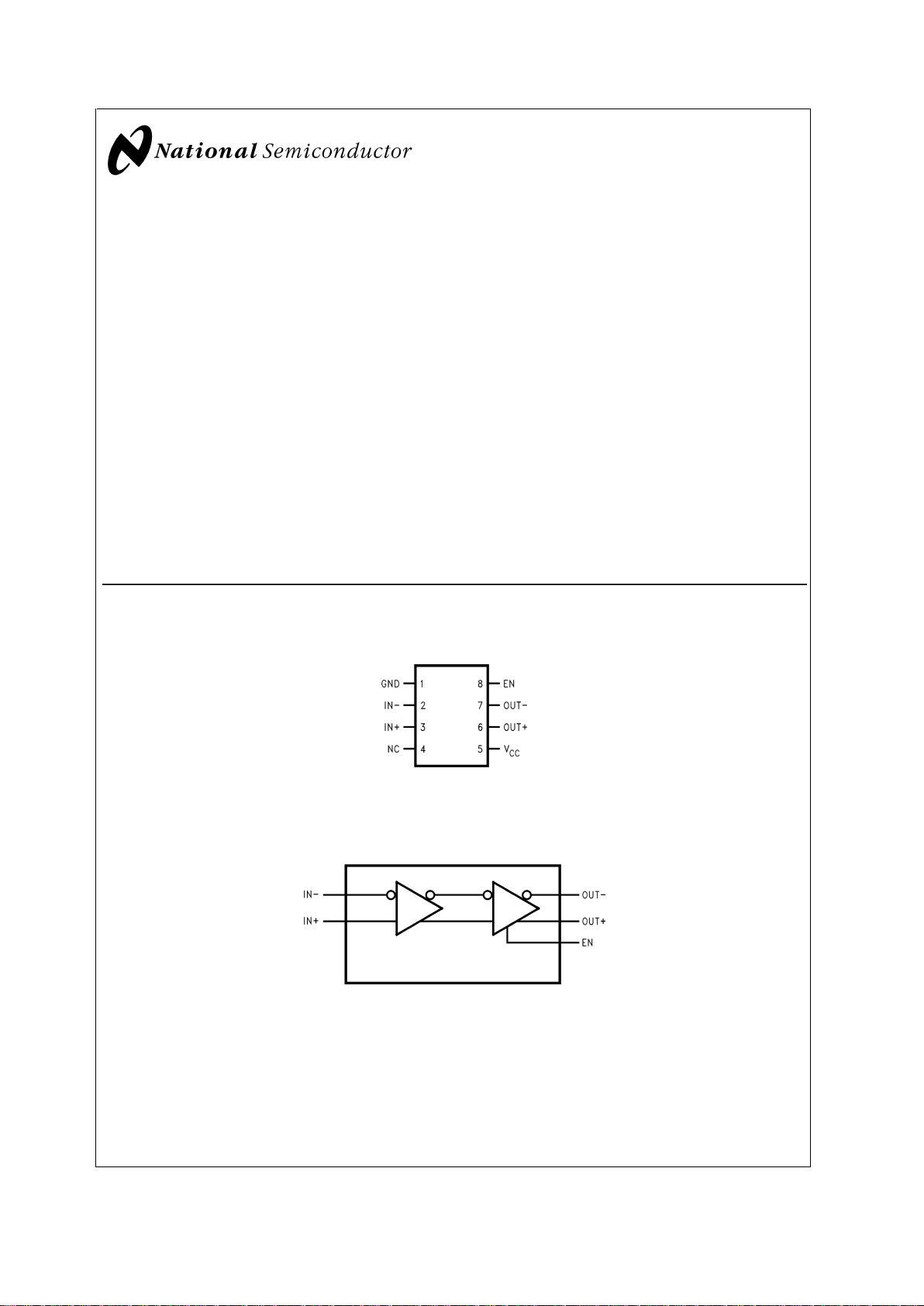
Connection Diagram
Block Diagram
Top View
DS101338-5
Order Number DS90LV001TM, DS90LV001TLD
See NS Package Number M08A, LDA08A
DS101338-2
April 2001
DS90LV001 3.3V LVDS-LVDS Buffer
© 2001 National Semiconductor Corporation DS101338 www.national.com
Page 2
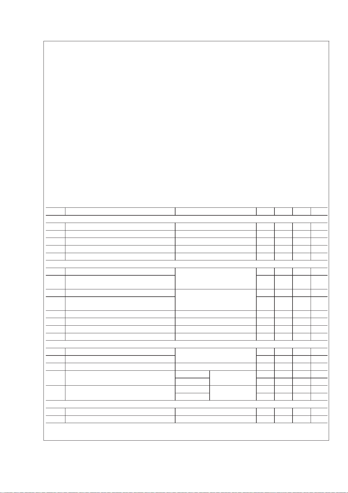
Absolute Maximum Ratings (Note 1)
If Military/Aerospace specified devices are required,
please contact the National Semiconductor Sales Office/
Distributors for availability and specifications.
Supply Voltage (V
CC
) −0.3V to +4V
LVCMOS/LVTTL Input Voltage
(EN)
−0.3V to (V
CC
+ 0.3V)
LVDS Receiver Input Voltage
(IN+, IN−) −0.3V to +4V
LVDS Driver Output Voltage
(OUT+, OUT−) −0.3V to +4V
LVDS Output Short Circuit
Current
Continuous
Junction Temperature +150˚C
Storage Temperature Range −65˚C to +150˚C
Lead Temperature Range
Soldering (4 sec.) +260˚C
Maximum Package Power Dissipation at 25˚C
M Package 726 mW
Derate M Package 5.8 mW/˚C above +25˚C
LDA Package 2.44 W
Derate LDA Package 19.49 mW/˚C above
+25˚C
ESD Ratings
(HBM, 1.5kΩ, 100pF) ≥2.5kV
(EIAJ, 0Ω, 200pF) ≥250V
Recommended Operating
Conditions
Min Typ Max Units
Supply Voltage (V
CC
) 3.0 3.3 3.6 V
Receiver Input Voltage 0 V
CC
V
Operating Free Air
Temperature
−40 +25 +85 ˚C
Electrical Characteristics
Over recommended operating supply and temperature ranges unless otherwise specified. (Notes 2, 3)
Symbol Parameter Conditions Min Typ Max Units
LVCMOS/LVTTL DC SPECIFICATIONS (EN)
V
IH
High Level Input Voltage 2.0 V
CC
V
V
IL
Low Level Input Voltage GND 0.8 V
I
IH
High Level Input Current VIN= 3.6V or 2.0V, VCC= 3.6V +7 +20 µA
I
IL
Low Level Input Current VIN= GND or 0.8V, VCC= 3.6V
±
1
±
10 µA
V
CL
Input Clamp Voltage ICL= −18 mA −0.6 −1.5 V
LVDS OUTPUT DC SPECIFICATIONS (OUT)
V
OD
Differential Output Voltage RL= 100Ω 250 325 450 mV
∆V
OD
Change in Magnitude of VODfor Complimentary
Output States
Figure 1
and
Figure 2
20 mV
V
OS
Offset Voltage RL= 100Ω 1.080 1.19 1.375 V
∆V
OS
Change in Magnitude of VOSfor Complimentary
Output States
Figure 1
20 mV
I
OZ
Output TRI-STATE Current EN = 0V, V
OUT=VCC
or GND
±
1
±
10 µA
I
OFF
Power-Off Leakage Current VCC= 0V, V
OUT
= 3.6V or GND
±
1
±
10 µA
I
OS
Output Short Circuit Current (Note 4) EN = VCC,V
OUT+
and V
OUT−
= 0V −16 −24 mA
I
OSD
Differential Output Short Circuit Current (Note 4) EN = VCC,VOD= 0V −7 −12 mA
LVDS RECEIVER DC SPECIFICATIONS (IN)
V
TH
Differential Input High Threshold VCM= +0.05V, +1.2V or +3.25V 0 +100 mV
V
TL
Differential Input Low Threshold −100 0 mV
V
CMR
Common Mode Voltage Range VID= 100mV, VCC= 3.3V 0.05 3.25 V
I
IN
Input Current VIN= +3.0V VCC= 3.6V or 0V
±
1
±
10 µA
V
IN
=0V
±
1
±
10 µA
∆I
IN
Change in Magnitude of I
IN
VIN= +3.0V VCC= 3.6V or 0V 1 6 µA
V
IN
=0V 1 6 µA
SUPPLY CURRENT
I
CCD
Total Supply Current EN = VCC,RL= 100Ω,CL=5pF 47 70 mA
I
CCZ
TRI-STATE Supply Current EN = 0V 22 35 mA
DS90LV001
www.national.com 2
Page 3
AC Electrical Characteristics
Over recommended operating supply and temperature ranges unless otherwise specified. (Note 3)
Symbol Parameter Conditions Min Typ Max Units
t
PHLD
Differential Propagation Delay High to Low RL= 100Ω,CL= 5pF 1.0 1.4 2.0 ns
t
PLHD
Differential Propagation Delay Low to High
Figure 3
and
Figure 4
1.0 1.4 2.0 ns
t
SKD1
Pulse Skew |t
PLHD−tPHLD
| (Note 5) (Note 6) 20 200 ps
t
SKD3
Part to Part Skew (Note 5) (Note 7) 0 60 ps
t
SKD4
Part to Part Skew (Note 5) (Note 8) 400 ps
t
LHT
Rise Time (Note 5) RL= 100Ω,CL= 5pF 200 320 450 ps
t
HLT
Fall Time (Note 5)
Figure 3
and
Figure 5
200 310 450 ps
t
PHZ
Disable Time (Active High to Z) RL= 100Ω,CL= 5pF 3 25 ns
t
PLZ
Disable Time (Active Low to Z)
Figure 6
and
Figure 7
325ns
t
PZH
Enable Time (Z to Active High) 25 45 ns
t
PZL
Enable Time (Z to Active Low) 25 45 ns
t
DJ
LVDS Data Jitter, Deterministic (Peak-to-Peak)
(Note 9)
VID= 300mV; PRBS = 223− 1 data;
V
CM
= 1.2V at 800Mbps (NRZ)
100 135 ps
t
RJ
LVDS Clock Jitter, Random (Note 9) VID= 300mV; VCM= 1.2V at 400MHz
clock
2.2 3.5 ps
Note 1: “Absolute Maximum Ratings” are those values beyond which the safety of the device cannot be guaranteed. They are not meant to imply that the device
should be operated at these limits. The table of “Electrical Characteristics” specifies conditions of device operation.
Note 2: Current into device pins is defined as positive. Current out of device pins is defined as negative. All voltages are referenced to ground except V
OD
and ∆VOD.
Note 3: All typical are given for V
CC
= +3.3V and TA= +25˚C, unless otherwise stated.
Note 4: Output short circuit current (I
OS
) is specified as magnitude only, minus sign indicates direction only.
Note 5: The parameters are guaranteed by design. The limits are based on statistical analysis of the device performance over the PVT (process, voltage and
temperature) range.
Note 6: t
SKD1
,|t
PLHD−tPHLD
|, is the magnitude difference in differential propagation delay time between the positive going edge and the negative going edge of
the same channel.
Note 7: t
SKD3
, Part to Part Skew, is defined as the difference between the minimum and maximum specified differential propagation delays. This specification
applies to devices at the same V
CC
and within 5˚C of each other within the operating temperature range.
Note 8: t
SKD4
, Part to Part Skew, is the differential channel-to- channel skew of any event between devices. This specification applies to devices over recommended
operating temperature and voltage ranges, and across process distribution. t
SKD4
is defined as |Max − Min| differential propagation delay.
Note 9: The parameters are guaranteed by design. The limits are based on statistical analysis of the device performance over the PVT range with the following test
equipment setup: HP8133A(patternpulse generator), 5 feet of RG142B cable with DUT test board and HP83480A (digital scope mainframe) with HP83484A(50GHz
scope module). The HP8133A with RG142B cable exhibit a t
DJ
= 21ps and tRJ= 1.8ps.
DS90LV001
www.national.com3
Page 4
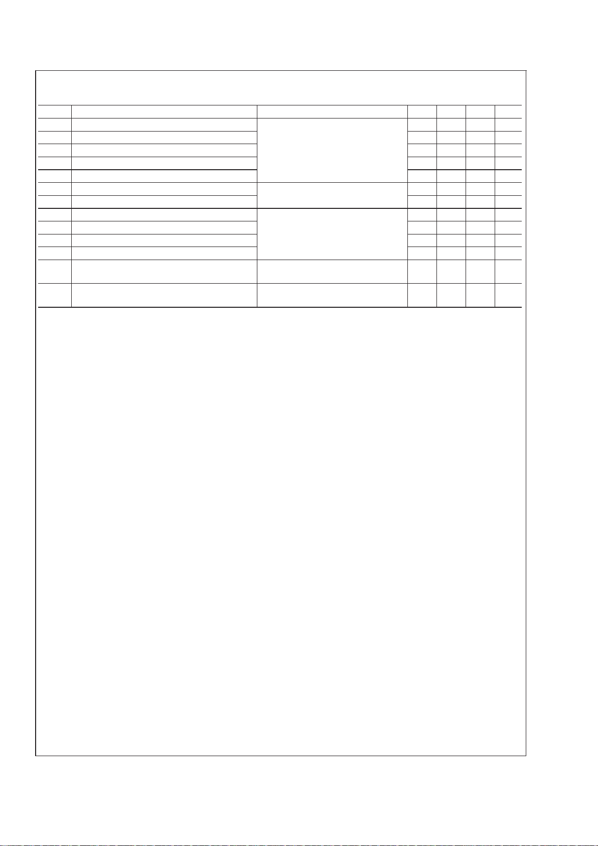
DC Test Circuits
AC Test Circuits and Timing Diagrams
DS101338-3
FIGURE 1. Differential Driver DC Test Circuit
DS101338-8
FIGURE 2. Differential Driver Full Load DC Test Circuit
DS101338-6
FIGURE 3. LVDS Output Load
DS101338-7
FIGURE 4. Propagation Delay Low-to-High and High-to-Low
DS101338-9
FIGURE 5. LVDS Output Transition Time
DS90LV001
www.national.com 4
Page 5

AC Test Circuits and Timing Diagrams (Continued)
DS101338-1
FIGURE 6. TRI-STATE Delay Test Circuit
DS101338-4
FIGURE 7. Output active to TRI-STATE and TRI-STATE to active output time
DS90LV001
www.national.com5
Page 6

DS90LV001 Pin Description (SOIC and LLP)
Pin Name Pin # Input/Output Description
GND 1 P Ground
IN − 2 I Inverting receiver LVDS input pin
IN+ 3 I Non-inverting receiver LVDS input pin
NC 4 No Connect
V
CC
5 P Power Supply, 3.3V±0.3V.
OUT+ 6 O Non-inverting driver LVDS output pin
OUT - 7 O Inverting driver LVDS output pin
EN 8 I Enable pin. When EN is LOW, the driver is disabled and the LVDS
outputs are in TRI-STATE. When EN is HIGH, the driver is enabled.
LVCMOS/LVTTL levels.
Typical Applications
Backplane Stub-Hider Application
DS101338-11
Cable Repeater Application
DS101338-10
DS90LV001
www.national.com 6
Page 7

Application Information
Mode of Operation:
The DS90LV001 can be used as a ’stub-hider.’ In many
systems, signals are distributed across backplanes, and one
of the limiting factors for system speed is the ’stub length’ or
the distance between the transmission line and the unterminated receivers on the individual cards. Although it is generally recognized that this distance should be as short as
possible to maximize system performance, real-world packaging concerns and PCB designs often make it difficult to
make the stubs as short as the designer would like. The
DS90LV001, available in the LLP (Leadless Leadframe
Package) package, can improve system performance by
allowing the receiver to be placed very close to the main
transmission line either on the backplane itself or very close
to the connector on the card. Longer traces to the LVDS
receiver may be placed after the DS90LV001. This very
small LLP package is a 75% space savings over the SOIC
package.
Input failsafe:
The receiver inputs of the DS90LV001 do not have internal
failsafe biasing. For point-to-point and multidrop applications
with a single source, failsafe biasing may not be required.
When the driver is off, the link is in-active. If failsafe biasing
is required, this can be accomplished with external high
value resistors. Using the equations in the LVDS Owner’s
Manual Chapter 4, the IN+ should be pull to V
CC
(3.3V) with
20kΩ and the IN− should be pull to GND with 12kΩ. This
provides a slight positive differential bias, and sets a known
HIGH state on the link with a minimum amount of distortion.
PCB Layout and Power System Bypass:
Circuit board layout and stack-up forthe DS90LV001 should
be designed to provide noise-free power to the device. Good
layout practice also will separate high frequency or high level
inputs and outputs to minimize unwanted stray noise pickup,
feedback and interference. Power system performance may
be greatly improved by using thin dielectrics (4 to 10 mils) for
power/ground sandwiches. This increases the intrinsic capacitance of the PCB power system which improves power
supply filtering, especially at high frequencies, and makes
the value and placement of external bypass capacitors less
critical. External bypass capacitors should include both RF
ceramic and tantalum electrolytic types. RF capacitors may
use values in the range 0.01 µF to 0.1 µF. Tantalum capacitors may be in the range 2.2 µF to 10 µF. Voltage rating for
tantalum capacitors should be at least 5X the power supply
voltage being used. It is recommended practice to use two
vias at each power pin of the DS90LV001 as well as all RF
bypass capacitor terminals. Dual vias reduce the interconnect inductance by up to half, thereby reducing interconnect
inductance and extending the effective frequency range of
the bypass components.
The outer layers of the PCB may be flooded with additional
ground plane. These planes will improve shielding and isolation as well as increase the intrinsic capacitance of the
power supply plane system. Naturally, to be effective, these
planes must be tied to the ground supply plane at frequent
intervals with vias. Frequent via placement also improves
signal integrity on signal transmission lines by providing
short paths for image currents which reduces signal distortion. The planes should be pulled back from alltransmission
lines and component mounting pads a distance equal to the
width of the widest transmission line or the thickness of the
dielectric separating the transmission line from the internal
power or ground plane(s) whichever is greater. Doing so
minimizes effects on transmission line impedances and reduces unwanted parasitic capacitances at component
mounting pads.
There are more common practices which should be followed
when designing PCBs for LVDS signaling. Please see application note AN-1108 for guidelines. In addition, application
note AN-1187 has additional information specifically related
to LLP recommendations.
DS101338-15
DS90LV001
www.national.com7
Page 8

Typical Performance Curves
Output High Voltage vs
Power Supply Voltage
DS101338-16
Output Low Voltage vs
Power Supply Voltage
DS101338-17
Output Short Circuit Current vs
Power Supply Voltage
DS101338-18
Differential Output Short Circuit Current vs
Power Supply Voltage
DS101338-19
Output TRI-STATE Current vs
Power Supply Voltage
DS101338-20
Offset Voltage vs
Power Supply Voltage
DS101338-21
DS90LV001
www.national.com 8
Page 9

Typical Performance Curves (Continued)
Differential Output Voltage
vs Power Supply Voltage
DS101338-22
Differential Output Voltage
vs Load Resistor
DS101338-23
Power Supply Current
vs Frequency
DS101338-24
Power Supply Current vs
Power Supply Voltage
DS101338-25
TRI-STATE Power Supply Current vs
Power Supply Voltage
DS101338-26
Differential Transition Voltage vs
Power Supply Voltage
DS101338-27
DS90LV001
www.national.com9
Page 10

Typical Performance Curves (Continued)
Differential Propagation Delay vs
Power Supply Voltage
DS101338-28
Differential Propagation Delay vs
Ambient Temperature
DS101338-36
Differential Skew vs
Power Supply Voltage
DS101338-29
Differential Skew vs
Ambient Temperature
DS101338-37
Transition Time vs
Power Supply Voltage
DS101338-30
Transition Time vs
Ambient Temperature
DS101338-38
DS90LV001
www.national.com 10
Page 11

Typical Performance Curves (Continued)
Differential Propagation Delay vs
Differential Input Voltage
DS101338-31
Differential Propagation Delay vs
Common-Mode Voltage
DS101338-32
Peak-to-Peak Output Jitter at VCM= 0.4V vs
Differential Input Voltage
DS101338-33
Peak-to-Peak Output Jitter at VCM= 2.9V vs
Differential Input Voltage
DS101338-35
Peak-to-Peak Output Jitter at VCM= 1.2V vs
Differential Input Voltage
DS101338-34
Peak-to-Peak Output Jitter at VCM= 1.2V vs
Ambient Temperature
DS101338-39
DS90LV001
www.national.com11
Page 12

Physical Dimensions inches (millimeters) unless otherwise noted
Order Number DS90LV001TM
See NS Package Number M08A
Order Number DS90LV001TLD
See NS Package Number LDA08A
DS90LV001
www.national.com 12
Page 13

Notes
LIFE SUPPORT POLICY
NATIONAL’S PRODUCTS ARE NOT AUTHORIZED FOR USE AS CRITICAL COMPONENTS IN LIFE SUPPORT
DEVICES OR SYSTEMS WITHOUT THE EXPRESS WRITTEN APPROVAL OF THE PRESIDENT AND GENERAL
COUNSEL OF NATIONAL SEMICONDUCTOR CORPORATION. As used herein:
1. Life support devices or systems are devices or
systems which, (a) are intended for surgical implant
into the body, or (b) support or sustain life, and
whose failure to perform when properly used in
accordance with instructions for use provided in the
labeling, can be reasonably expected to result in a
significant injury to the user.
2. A critical component is any component of a life
support device or system whose failure to perform
can be reasonably expected to cause the failure of
the life support device or system, or to affect its
safety or effectiveness.
National Semiconductor
Corporation
Americas
Tel: 1-800-272-9959
Fax: 1-800-737-7018
Email: support@nsc.com
National Semiconductor
Europe
Fax: +49 (0) 180-530 85 86
Email: europe.support@nsc.com
Deutsch Tel: +49 (0) 69 9508 6208
English Tel: +44 (0) 870 24 0 2171
Français Tel: +33 (0) 1 41 91 8790
National Semiconductor
Asia Pacific Customer
Response Group
Tel: 65-2544466
Fax: 65-2504466
Email: ap.support@nsc.com
National Semiconductor
Japan Ltd.
Tel: 81-3-5639-7560
Fax: 81-3-5639-7507
www.national.com
 Loading...