

Page 1
DS90CR483 / DS90CR484
48-Bit LVDS Channel Link Serializer/Deserializer
General Description
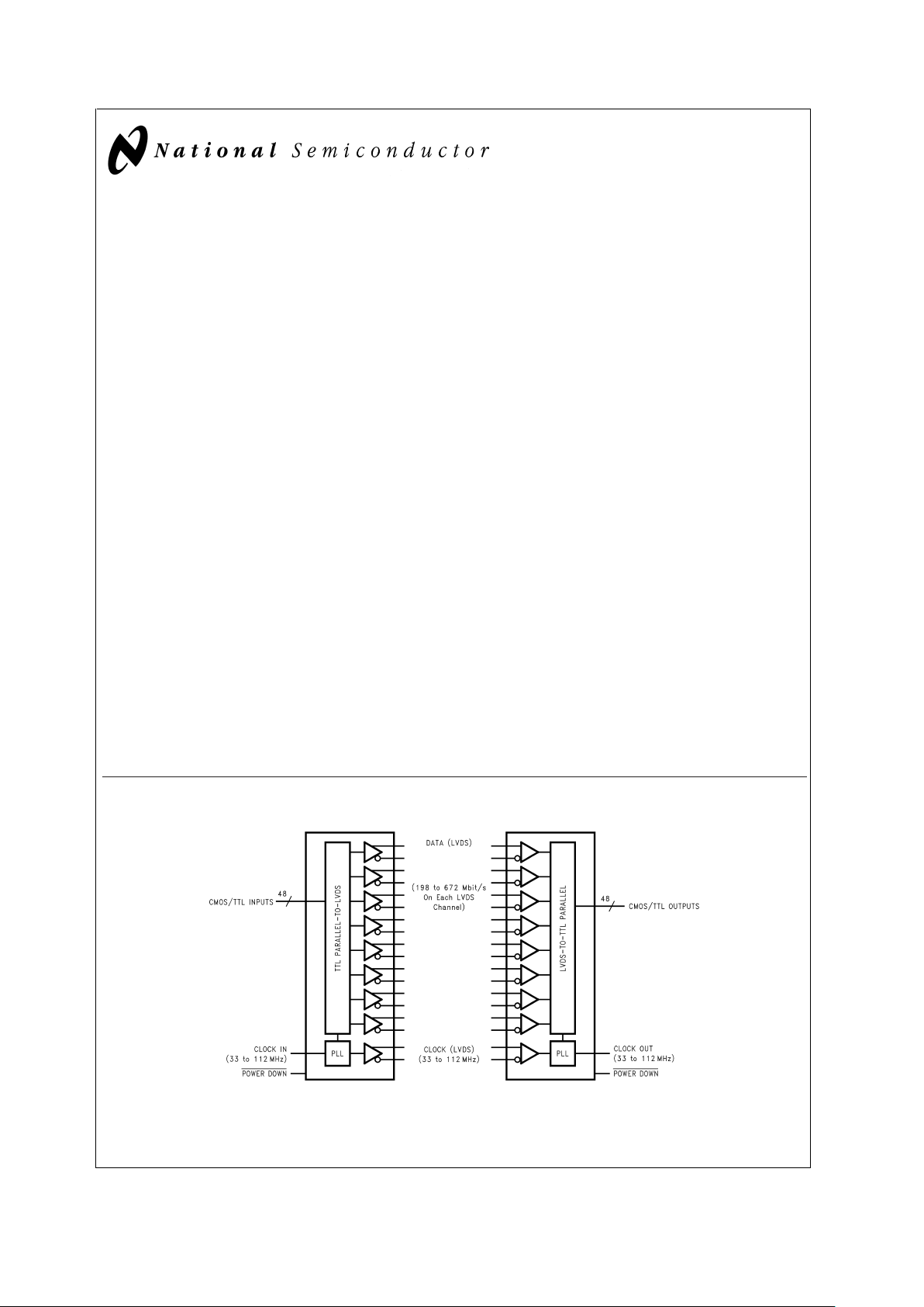
The DS90CR483 transmitter converts 48 bits of CMOS/TTL
data into eight LVDS (Low Voltage Differential Signaling)
data streams.Aphase-locked transmit clockis transmitted in
parallel with the data streams over a ninth LVDS link. Every
cycle of the transmit clock 48 bits of input data are sampled
and transmitted. The DS90CR484 receiver converts the
LVDS data streams back into 48 bits of CMOS/TTL data. At
a transmit clock frequency of 112MHz, 48 bits of TTL data
are transmitted at a rate of 672Mbps per LVDSdata channel.
Using a 112MHz clock, the data throughput is 5.38Gbit/s
(672Mbytes/s).
The multiplexing of data lines provides a substantial cable
reduction. Long distance parallel single-ended buses typically require a ground wire per active signal (and have very
limited noise rejection capability). Thus, for a 48-bit wide
data and one clock, up to 98 conductors are required. With
this Channel Link chipset as few as 19 conductors (8 data
pairs, 1 clock pair and a minimum of one ground) are
needed. This provides an 80% reduction in cable width,
which provides a system cost savings, reduces connector
physical size and cost, and reduces shielding requirements
due to the cables’ smaller form factor.
The 48 CMOS/TTL inputs can support a variety of signal
combinations. For example, 6 8-bit words or 5 9-bit (byte +
parity) and 3 controls.
The DS90CR483/DS90CR484 chipset is improved over prior
generations of Channel Link devices and offers higher bandwidth support and longer cable drive with three areas of enhancement. To increase bandwidth, the maximum clock rate
is increased to 112 MHz and 8 serialized LVDS outputs are
provided. Cable drive is enhanced with a user selectable
pre-emphasis feature that provides additional output current
during transitions to counteract cable loading effects. DC
balancing on a cycle-to-cycle basis, is also provided to reduce ISI (Inter-Symbol Interference). With pre-emphasis and
DC balancing, a low distortion eye-pattern is provided at the
receiver end of the cable. A cable deskew capability has
been added to deskew long cables of pair-to-pair skew of up
to +/−1 LVDS data bit time (up to 80 MHz Clock Rate). These
three enhancements allow cables 5+ meters in length to be
driven.
The chipset is an ideal means to solve EMI and cable size
problems associated with wide, high speed TTL interfaces.
For more details, please refer to the “Applications Information” section of this datasheet.
Features
n Up to 5.38 Gbits/sec bandwidth
n 33 MHz to 112 MHz input clock support
n LVDS SER/DES reduces cable and connector size
n Pre-emphasis reduces cable loading effects
n DC balance data transmission provided by transmitter
reduces ISI distortion
n Cable Deskew of +/−1 LVDS data bit time (up to 80
MHz Clock Rate)
n 5V Tolerant TxIN and control input pins
n Flow through pinout for easy PCB design
n +3.3V supply voltage
n Transmitter rejects cycle-to-cycle jitter
n Conforms to ANSI/TIA/EIA-644-1995 LVDS Standard
Generalized Block Diagrams
TRI-STATE®is a registered trademark of National Semiconductor Corporation.
DS100918-1
February 2000
DS90CR483/DS90CR484 48-Bit LVDS Channel Link Serializer / Deserializer
© 2000 National Semiconductor Corporation DS100918 www.national.com
Page 2
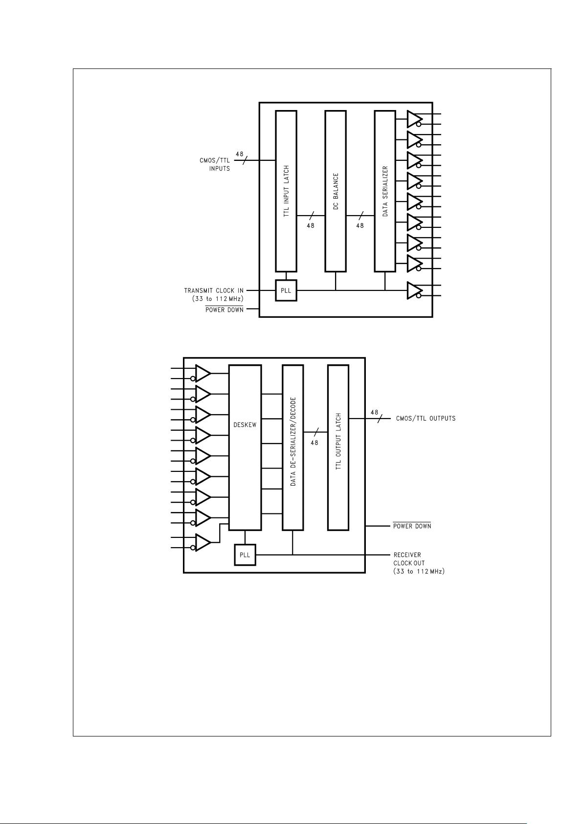
Generalized Transmitter Block Diagram
Generalized Receiver Block Diagram
DS100918-2
DS100918-3
DS90CR483/DS90CR484
www.national.com 2
Page 3
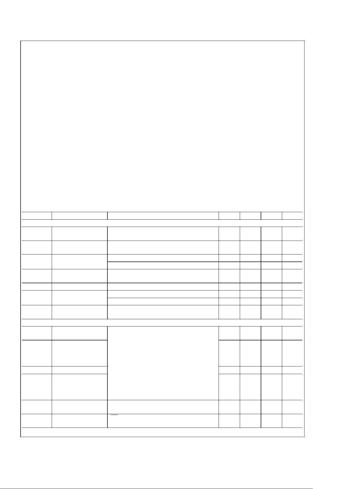
Absolute Maximum Ratings (Note 1)
If Military/Aerospace specified devices are required,
please contact the National Semiconductor Sales Office/
Distributors for availability and specifications.
Supply Voltage (V
CC
) −0.3V to +4V
CMOS/TTL Input Voltage −0.3V to +5.5V
CMOS/TTL Output
Voltage −0.3V to (V
CC
+ 0.3V)
LVDS Receiver Input
Voltage −0.3V to +3.6V
LVDS Driver Output
Voltage −0.3V to +3.6V
LVDS Output Short Circuit
Duration Continuous
Junction Temperature +150˚C
Storage Temperature −65˚C to +150˚C
Lead Temperature
(Soldering, 4 sec.) +260˚C
Maximum Package Power Dissipation Capacity
@
25˚C
100 TQFP Package:
DS90CR483 2.8W
DS90CR484 2.8W
Package Derating:
DS90CR483 18.2mW/˚C above +25˚C
DS90CR484 18.2mW/˚C above +25˚C
ESD Rating:
DS90CR483
(HBM, 1.5kΩ, 100pF)
>
6kV
(EIAJ, 0Ω, 200pF)
>
300 V
DS90CR484
(HBM, 1.5kΩ, 100pF)
>
2kV
(EIAJ, 0Ω, 200pF)
>
200 V
Recommended Operating
Conditions
Min Nom Max Units
Supply Voltage (V
CC
) 3.0 3.3 3.6 V
Operating Free Air
Temperature (T
A)
−10 +25 +70 ˚C
Receiver Input Range 0 2.4 V
Supply Noise Voltage (V
CC
) 100 mV
p-p
Electrical Characteristics
Over recommended operating supply and temperature ranges unless otherwise specified.
Symbol Parameter Conditions Min Typ Max Units
CMOS/TTL DC SPECIFICATIONS
V
IH
High Level Input
Voltage
2.0 V
CC
V
V
IL
Low Level Input
Voltage
GND 0.8 V
V
OH
High Level Output
Voltage
IOH= −0.4 mA 2.7 2.9 V
I
OH
= −2mA 2.7 2.85 V
V
OL
Low Level Output
Voltage
IOL= 2 mA 0.1 0.3 V
V
CL
Input Clamp Voltage ICL= −18 mA −0.79 −1.5 V
I
IN
Input Current VIN= 0.4V, 2.5V or V
CC
+1.8 +15 µA
V
IN
= GND −15 0 µA
I
OS
Output Short Circuit
Current
V
OUT
= 0V −120 mA
LVDS DRIVER DC SPECIFICATIONS
V
OD
Differential Output
Voltage
RL= 100Ω 250 345 450 mV
∆V
OD
Change in V
OD
between
Complimentary Output
States
35 mV
V
os
Offset Voltage 1.125 1.25 1.375 V
∆V
os
Change in V
os
between
Complimentary Output
States
35 mV
I
OS
Output Short Circuit
Current
V
OUT
= 0V, RL= 100Ω −3.5 −5 mA
I
OZ
Output TRI-STATE
®
Current
PD = 0V, V
OUT
=0VorV
CC
±
1
±
10 µA
DS90CR483/DS90CR484
www.national.com3
Page 4
Electrical Characteristics (Continued)
Over recommended operating supply and temperature ranges unless otherwise specified.
Symbol Parameter Conditions Min Typ Max Units
LVDS RECEIVER DC SPECIFICATIONS
V
TH
Differential Input High
Threshold
VCM= +1.2V +100 mV
V
TL
Differential Input Low
Threshold
−100 mV
I
IN
Input Current VIN= +2.4V, VCC= 3.6V
±
10 µA
V
IN
= 0V, VCC= 3.6V
±
10 µA
TRANSMITTER SUPPLY CURRENT
ICCTW Transmitter Supply
Current
Worst Case
R
L
= 100Ω,CL= 5 pF,
Worst Case Pattern
(
Figures 1, 2
)
f = 33 MHz 91.4 140 mA
f = 66 MHz 106 160 mA
f = 112 MHz 155 190 mA
ICCTZ Transmitter Supply
Current
Power Down
PD = Low
550µA
Driver Outputs in TRI-STATE under Powerdown
Mode
RECEIVER SUPPLY CURRENT
ICCRW Receiver Supply
Current
Worst Case
C
L
= 8 pF,
Worst Case Pattern
(
Figures 1, 3
)
f = 33 MHz 125 150 mA
f = 66 MHz 215 250 mA
f = 112 MHz 350 380 mA
ICCRZ Receiver Supply
Current
Power Down
PD = LowReceiver Outputs stay low during
Power down mode.
20 100 µA
Recommended Transmitter Input Characteristics
Over recommended operating supply and temperature ranges unless otherwise specified.
Symbol Parameter Min Typ Max Units
TCIT TxCLK IN Transition Time (
Figure 4
) 1.0 2.0 3.0 ns
TCIP TxCLK IN Period (
Figure 5
) 8.928 T 30.3 ns
TCIH TxCLK in High Time (
Figure 5
) 0.35T 0.5T 0.65T ns
TCIL TxCLK in Low Time (
Figure 5
) 0.35T 0.5T 0.65T ns
TXIT TxIN Transition Time 1.5 6.0 ns
Transmitter Switching Characteristics
Over recommended operating supply and temperature ranges unless otherwise specified.
Symbol Parameter Min Typ Max Units
LLHT LVDS Low-to-High Transition Time, (
Figure 2
),
PRE = 0.75V (disabled)
0.14 0.7 ns
LVDS Low-to-High Transition Time, (
Figure 2
),
PRE = Vcc (max)
0.11 0.6 ns
LHLT LVDS High-to-Low Transition Time, (
Figure 2
),
PRE = 0.75V (disabled)
0.16 0.8 ns
LVDS High-to-Low Transition Time, (
Figure 2
),
PRE = Vcc (max)
0.11 0.7 ns
TBIT Transmitter Bit Width 1/7 TCIP ns
TCCS TxOUT Channel to Channel Skew 100 ps
TSTC TxIN Setup to TxCLK IN, (
Figure 5
) 2.5 ns
THTC TxIN Hold to TxCLK IN, (
Figure 5
)0 ns
TPDL Transmitter Propagation Delay - Latency, (
Figure 7
) 1.5(TCIP)+3.72 1.5(TCIP)+4.4 1.5(TCIP)+6.24 ns
TPLLS Transmitter Phase Lock Loop Set, (
Figure 9
)10ms
TPDD Transmitter Powerdown Delay, (
Figure 11
) 100 ns
DS90CR483/DS90CR484
www.national.com 4
Page 5
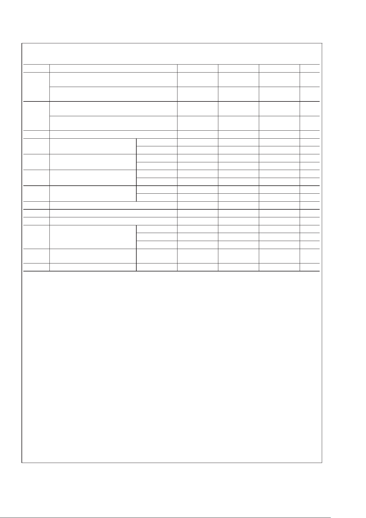
Receiver Switching Characteristics
Over recommended operating supply and temperature ranges unless otherwise specified.
Symbol Parameter Min Typ Max Units
CLHT CMOS/TTL Low-to-High Transition Time, (
Figure 3
),
Rx data out
2.0 ns
CMOS/TTL Low-to-High Transition Time, (
Figure 3
),
Rx clock out
1.0 ns
CHLT CMOS/TTL High-to-Low Transition Time, (
Figure 3
),
Rx data out
2.0 ns
CMOS/TTL High-to-Low Transition Time, (
Figure 3
),
Rx clock out
1.0 ns
RCOP RxCLK OUT Period, (
Figure 6
) 8.928 T 30.3 ns
RCOH RxCLK OUT High Time, (
Figure
6
), (Note 4)
f = 112 MHz 3.5 ns
f = 66 MHz 6.0 ns
RCOL RxCLK OUT Low Time, (
Figure 6
),
(Note 4)
f = 112 MHz 3.5 ns
f = 66 MHz 6.0 ns
RSRC RxOUT Setup to RxCLK OUT,
(
Figure 6
), (Note 4)
f = 112 MHz 2.4 ns
f = 66 MHz 3.6 ns
RHRC RxOUT Hold to RxCLK OUT,
(
Figure 6
), (Note 4)
f = 112 MHz 3.4 ns
f = 66 MHz 7.0 ns
RPDL Receiver Propagation Delay - Latency, (
Figure 8
) 3(TCIP)+4.0 3(TCIP)+4.8 3(TCIP)+6.5 ns
RPLLS Receiver Phase Lock Loop Set ,(
Figure 10
)10ms
RPDD Receiver Powerdown Delay, (
Figure 12
)1µs
RSKM Receiver Skew Margin without
Deskew, (
Figure 13
), (Notes 4, 5)
f = 112 MHz 170 210 ps
f = 85 MHz 160 200 ps
f = 66 MHz 210 275 ps
RDR Receiver Deskew Range f = 80 MHz
±
1.786
(
±
1TBIT)
(
±
1.3 TBIT) ns
RDSS Receiver Deskew Step Size f = 80 MHz 0.3 TBIT ns
Note 1: “Absolute Maximum Ratings” are those values beyond which the safety of the device cannot be guaranteed. They are not meant to imply that the device
should be operated at these limits. The tables of “Electrical Characteristics” specify conditions for device operation.
Note 2: Typical values are given for V
CC
= 3.3V and TA= +25˚C.
Note 3: Current into device pins is defined as positive. Current out of device pins is defined as negative. Voltagesare referenced to ground unless otherwise specified (except V
TH,VTL,VOD
and ∆VOD).
Note 4: The Minimum and Maximum Limits are based on statistical analysis of the device performance over voltage and temperature ranges. This parameter is functionally tested on Automatic Test Equipment (ATE). ATE is limited to 85MHz. A sample of characterization parts have been bench tested to verify functional performance.
Note 5: Receiver Skew Margin is defined as the valid data sampling region at the receiver inputs. This margin takes into account transmitter output pulse positions
(min and max) and the receiver input setup and hold time (internal data sampling window - RSPOS). This margin allows for LVDS interconnect skew, inter-symbol
interference (both dependent on type/length of cable) and clock jitter.
RSKM ≥ cable skew (type, length) + source clock jitter (cycle to cycle).
DS90CR483/DS90CR484
www.national.com5
Page 6
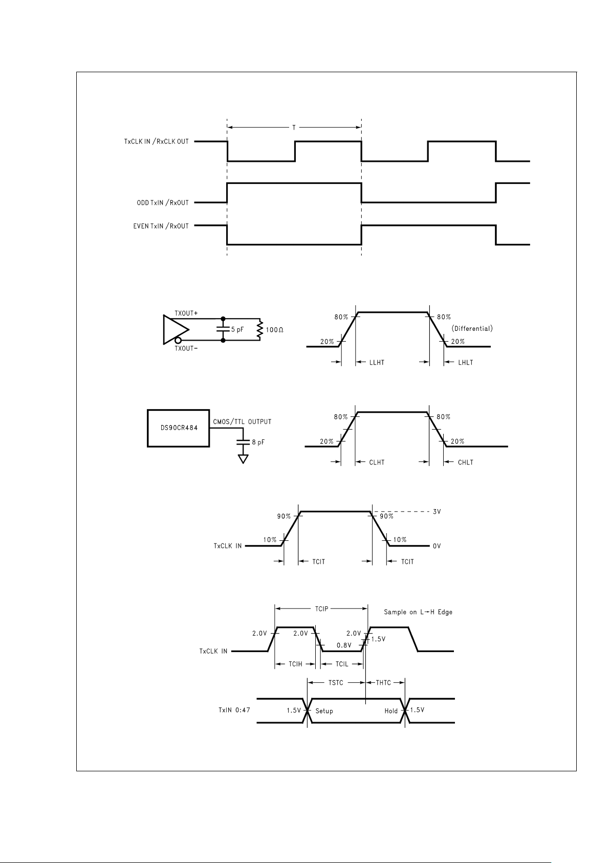
AC Timing Diagrams
Note 6: The worst case test pattern produces a maximum toggling of digital circuits, LVDS I/O and CMOS/TTL I/O.
DS100918-10
FIGURE 1. “Worst Case” Test Pattern
DS100918-12
FIGURE 2. DS90CR483 (Transmitter) LVDS Output Load and Transition Times
DS100918-13
FIGURE 3. DS90CR484 (Receiver) CMOS/TTL Output Load and Transition Times
DS100918-14
FIGURE 4. DS90CR483 (Transmitter) Input Clock Transition Time
DS100918-15
FIGURE 5. DS90CR483 (Transmitter) Setup/Hold and High/Low Times
DS90CR483/DS90CR484
www.national.com 6
Page 7

AC Timing Diagrams (Continued)
DS100918-16
FIGURE 6. DS90CR484 (Receiver) Setup/Hold and High/Low Times
DS100918-27
FIGURE 7. DS90CR483 (Transmitter) Propagation Delay - Latency (Rising Edge Strobe)
DS100918-28
FIGURE 8. DS90CR484 (Receiver) Propagation Delay - Latency (Rising Edge Strobe)
DS90CR483/DS90CR484
www.national.com7
Page 8

AC Timing Diagrams (Continued)
DS100918-19
FIGURE 9. DS90CR483 (Transmitter) Phase Lock Loop Set Time
DS100918-20
FIGURE 10. DS90CR484 (Receiver) Phase Lock Loop Set Time
DS100918-21
FIGURE 11. Transmitter Power Down Delay
DS90CR483/DS90CR484
www.national.com 8
Page 9

AC Timing Diagrams (Continued)
DS100918-22
FIGURE 12. Receiver Power Down Delay
DS100918-25
C—Setup and Hold Time (Internal data sampling window) defined by Rspos (receiver input strobe position) min and max
Tppos—Transmitter output pulse position (min and max)
RSKM = Cable Skew (type, length) + LVDS Source Clock Jitter (cycle to cycle) (Note 7) + ISI (Inter-symbol interference) (Note 8)
Cable Skew — typically 10 ps–40 ps per foot, media dependent
Note 7: Cycle-to-cycle LVDS Output jitter is less than 100 ps (worse case estimate).
Note 8: ISI is dependent on interconnect length; may be zero
FIGURE 13. Receiver Skew Margin
DS90CR483/DS90CR484
www.national.com9
Page 10

LVDS Interface
DS100918-4
FIGURE 14. 48 Parallel TTL Data Inputs Mapped to LVDS Outputs
DS90CR483/DS90CR484
www.national.com 10
Page 11

DS90CR483 Pin Description—Channel Link Transmitter
Pin Name I/O No. Description
TxIN I 48 TTL level input. (Note 9).
TxOUTP O 8 Positive LVDS differential data output.
TxOUTM O 8 Negative LVDS differential data output.
TxCLKIN I 1 TTL level clock input. The rising edge acts as data strobe.
TxCLKP O 1 Positive LVDS differential clock output.
TxCLKM O 1 Negative LVDS differential clock output.
PD
I 1 TTL level input. Assertion (low input) tri-states the outputs, ensuring low
current at power down. (Note 9).
PLLSEL I 1 PLL range select. This pin must be tied to V
CC
. NC or tied to Ground is
reserved for future use. (Note 9)
PRE I 1 Pre-emphasis “level” select. Pre-emphasis is active when input is tied to
V
CC
through external pull-up resistor. Resistor value determines
Pre-emphasis level (See Applications Information Section). For normal
LVDS drive level (No Pre-emphasis) leave this pin open (do not tie to
ground).
DS_OPT I 1 Cable Deskew performed when TTL level input is low. No TxIN data is
sampled during Deskew. To perform Deskew function, input must be held
low for a minimum of 4 clock cycles. The Deskew operation is normally
conducted after the TX and RX PLLs have locked. It should also be
conducted after a system reset, or a reconfiguration event. It must be
peformed at least once when ″DESKEW″ is enabled. (Note 9)
V
CC
I 8 Power supply pins for TTL inputs and digital circuitry.
GND I 5 Ground pins for TTL inputs and digital circuitry.
PLLV
CC
I 2 Power supply pin for PLL circuitry.
PLLGND I 3 Ground pins for PLL circuitry.
LVDSV
CC
I 3 Power supply pin for LVDS outputs.
LVDSGND I 4 Ground pins for LVDS outputs.
NC 4 No Connect. Make NO Connection to these pins - leave open.
Note 9: Inputs default to “low” when left open due to internal pull-down resistor.
DS90CR483/DS90CR484
www.national.com11
Page 12

DS90CR484 Pin Description—Channel Link Receiver
Pin Name I/O No. Description
RxINP I 8 Positive LVDS differential data inputs.
RxINM I 8 Negative LVDS differential data inputs.
RxOUT O 48 TTL level data outputs. In PowerDown (PD = Low) mode, receiver outputs
are forced to a Low state.
RxCLKP I 1 Positive LVDS differential clock input.
RxCLKM I 1 Negative LVDS differential clock input.
RxCLKOUT O 1 TTL level clock output. The rising edge acts as data strobe.
PLLSEL I 1 PLL range select. This pin must be tied to V
CC
. NC or tied to Ground is
reserved for future use. (Note 9)
DESKEW I 1 Deskew / Oversampling “on/off” select. When using the Deskew /
Oversample feature this pin must be tied to V
CC
. Tieing this pin to ground
disables this feature. (Note 9)
PD
I 1 TTL level input. When asserted (low input) the receiver outputs are Low.
(Note 9)
V
CC
I 8 Power supply pins for TTL outputs and digital circuitry.
GND I 8 Ground pins for TTL outputs and digital circuitry.
PLLV
CC
I 1 Power supply for PLL circuitry.
PLLGND I 2 Ground pin for PLL circuitry.
LVDSV
CC
I 2 Power supply pin for LVDS inputs.
LVDSGND I 3 Ground pins for LVDS inputs.
NC 6 No Connect. Make NO Connection to these pins - leave open.
Note 10: These receivers have input fail-safe bias circuitry to guarantee a stable receiver output for floating or terminated receiver inputs. Under test conditions receiver inputs will be in a HIGH state. If the cable inter-connect are disconnected which results in floating/terminated inputs, the outputs will remain in the last valid
state.
DS90CR483/DS90CR484
www.national.com 12
Page 13

Applications Information
The DS90CR483/DS90CR484 chipset is improved over prior
generations of Channel Link devices and offers higher bandwidth support and longer cable drive with three areas of enhancement. To increase bandwidth, the maximum clock rate
is increased to 112 MHz and 8 serialized LVDS outputs are
provided. Cable drive is enhanced with a user selectable
pre-emphasis feature that provides additional output current
during transitions to counteract cable loading effects. This
requires the use of one pull up resistor to Vcc; please refer to
the table “Pre-emphasis DC level with Rpre” below to set the
level needed. DC balancing on a cycle-to-cycle basis, is also
provided to reduce ISI (Inter-Symbol Interference). With
pre-emphasis and DC balancing, a low distortion eye-pattern
is provided at the receiver end of the cable. A cable deskew
capability has been added to deskew long cables of
pair-to-pair skew of up to +/−1 LVDS data bit time (up to 80
MHz clock rates). For detail on deskew, refer to “Deskew”
section of this application information. These three enhancements allow cables 5+ meters in length to be driven.
New features Description:
1. Pre-emphasis:Adds extra current during LVDSlogic tran-
sition to reduce the cable loading effects. Pre-emphasis
strength is set via a DC voltage level applied from min to max
(0.75V to Vcc) at the “PRE” pin.A higher input voltage on the
”PRE” pin increases the magnitude of dynamic current during data transition. The “PRE” pin requires one pull-up resistor (Rpre) to Vcc in order to set the DC level. There is an internal resistor network, which cause a voltage drop. Please
refer to the tables below to set the voltage level.
TABLE 1. Pre-emphasis DC voltage level with (Rpre)
Rpre Resulting PRE Voltage Effects
1MΩ or NC 0.75V Standard LVDS
50kΩ 1.0V
9kΩ 1.5V 50% pre-emphasis
3kΩ 2.0V
1kΩ 2.6V
100Ω Vcc 100% pre-emphasis
TABLE 2. Pre-emphasis needed per cable length
Frequency PRE Voltage Typical cable length
112MHz 1.0V 2 meters
112MHz 1.5V 5 meters
80MHz 1.0V 2 meters
80MHz 1.2V 5+ meters
66MHz 1.5V 5+ meters
Note 11: This is based on testing with standard shield twisted pair cable. The amount of pre-emphasis will vary depending on the type of cable, length and operating
frequency.
2. DC Balance: In addition to data information an additional
bit is transmitted on every LVDS data signal line during each
cycle as shown in
Figure 14
. This bit is the DC balance bit
(DCBAL). The purpose of the DC Balance bit is to minimize
the short- and long-term DC bias on the signal lines. This is
achieved by selectively sending the data either unmodified
or inverted.
The value of the DC balance bit is calculated from the running word disparity and the data disparity of the current word
to be sent. The data disparity of the current word shall be calculated by subtracting the number of bits of value 0 from the
number of bits value 1 in the current word. Initially, the running word disparity may be any value between +7 and −6.
The running word disparity shall be calculated as a continuous sum of all the modified data disparity values, where the
unmodified data disparity value is the calculated data disparity minus 1 if the data is sent unmodified and 1 plus the inverse of the calculated data disparity if the data is sent inverted. The value of the running word disparity shall saturate
at +7 and −6.
The value of the DC balance bit (DCBAL) shall be 0 when
the data is sent unmodified and 1 when the data is sent inverted. To determine whether to send data unmodified or inverted, the running word disparity and the current data disparity are used. If the running word disparity is positive and
the current data disparity is positive, the data shall be sent
inverted. If the running word disparity is positive and the current data disparity is zero or negative, the data shall be sent
unmodified. If the running word disparity is negative and the
current data disparity is positive, the data shall be sent unmodified. If the running word disparity is negative and the
current data disparity is zero or negative, the data shall be
sent inverted. If the running word disparity is zero, the data
shall be sent inverted.
Cable drive is enhanced with the user selectable
pre-emphasis feature that provides additional output current
during transitions to counteract cable loading effects. DC
balancing on a cycle-to-cycle basis, is also provided to reduce ISI (Inter-Symbol Interference). With pre-emphasis and
DC balancing, a low distortion eye-pattern is provided at the
receiver end of the cable. These enhancements allow cables
5+ meters in length to be driven depending upon media and
clock rate.
3. Deskew: The “DESKEW” pin on the receiver when set
high will deskew a minimum of
±
1 LVDS data bit time skew
between signals arriving on independent differential pairs
(pair-to-pair skew). It is required that the “DS_OPT” pin on
the Transmitter must be applied low for a minimum of four
clock cycles to complete the deskew operation. It is also required that this must be performed at least once at any time
after the PLL has locked to the input clock frequency. If
power is lost, or if the cable has been switched, this proce-
DS90CR483/DS90CR484
www.national.com13
Page 14

Applications Information (Continued)
dure must be repeated or else the receiver may not sample
the incoming LVDS data correctly. When the receiver is in
the deskew mode, all receiver outputs are set to a LOW
state. Setting the “DESKEW” pin to low will disable the
deskew operation and allow the receiver to operation on a
fixed data sampling strobe. In this case, the ”DS_OPT” pin
on the transmitter must then be set high.
The DS_OPT pin at the input of the transmitter
(DS90CR483) is used to initiate the deskew calibration pattern. It must be applied low for a minimum of four clock
cycles in order for the receiver to complete the deskew operation. For this reason, the LVDS clock signal with DS_OPT
applied high (active data sampling) shall be 1111000 or
1110000 pattern. During the deskew operation with DS_OPT
applied low, the LVDS clock signal shall be 1111100 or
1100000 pattern. The transmitter will also output a series of
1111000 or 1110000 onto the LVDS data lines (TxOUT 0-7)
during deskew so that the receiver can automatically calibrated the data sampling strobes at the receiver inputs. Each
data channel is deskewed independently and is tuned with a
step size of 1/3 of a bit time over a range of +/−1 TBIT. The
Deskew feature operates up to clock rates of 80 MHz only.
When using the DESKEW feature, the sampling strobe will
remain within the middle third of the LVDS sub symbol.
The Receiver is also able to tolerate a maximum of 300ps
skew between the signals arriving on a single differential pair
(intra-pair).
Clock Jitter:
The transmitter is designed to reject cycle-to-cycle jitter
which may be seen at the transmitter input clock. Very low
cycle-to-cycle jitter is passed on to the transmitter outputs.
Cycle-to-cyle jitter has been measured over frequency is
less than 100 ps. This should be subtracted from the RSKM
budget as shown and described in
Figure 13
. This rejection
capability significantly reduces the impact of jitter at the TXinput clock pin, and improves the accuracy of data sampling
in the receiver.
Power Down:
Both transmitter and receiver provide a power down feature.
When asserted current draw through the supply pins is minimized and the PLLs are shut down. The transmitter outputs
are in TRI-STATE when in power down mode. The receiver
outputs are forced to a active LOW state when in the power
down mode. (See Pin Description Tables).
Configurations:
The transmitter is designed to be connected typically to a
single receiver load. This is known as a point-to-point con-
figuration. It is also possible to drive multiple receiver loads if
certain restrictions are made. Only the final receiver at the
end of the interconnect should provide termination across
the pair. In this case, the driver still sees the intended DC
load of 100 Ohms. Receivers connected to the cable between the transmitter and the final receiver must not load
down the signal. To meet this system requirement, stub
lengths from the line to the receiver inputs must be kept very
short.
Cable Termination
A termination resistor is required for proper operation to be
obtained. The termination resistor should be equal to the differential impedance of the media being driven. This should
be in the range of 90 to 132 Ohms. 100 Ohms is a typical
value common used with standard 100 Ohm twisted pair
cables. This resistor is required for control of reflections and
also to complete the current loop. It should be placed as
close to the receiver inputs to minimize the stub length from
the resistor to the receiver input pins.
How to configure for backplane applications:
In a backplane application with differential line impedance of
100Ω the differential line pair-to-pair skew can controlled by
trace layout. The transmitter-DS90CR483 “DS_OPT” pin
may be set high. In a backplane application with short PCB
distance traces, pre-emphasis from the transmitter is typically not required. The “PRE” pin should be left open (do not
tie to ground). A resistor pad provision for a pull up resistor to
Vcc can be implemented in case pre-emphasis is needed to
counteract heavy capacitive loading effects.
How to configure for cable inter-connect applications:
In applications that require the long cable drive capability.
The DS90CR483/DS90CR484 chipset is improved over prior
generations of Channel Link devices and offers higher bandwidth support and longer cable drive with the use of DC balanced data transmission, pre-emphasis. Cable drive is enhanced with a user selectable pre-emphasis feature that
provides additional output current during transitions to counteract cable loading effects. This requires the use of one pull
up resistor to Vcc; please refer to the table “Pre-emphasis
DC level with Rpre” above to set the level needed. DC balancing on a cycle-to-cycle basis, is also provided to reduce
ISI (Inter-Symbol Interference). With pre-emphasis and DC
balancing, a low distortion eye-pattern is provided at the receiver end of the cable. These enhancements allow cables
5+ meters in length to be driven. Depending upon clock rate
and the media being driven, the cable Deskew feature may
also be employed - see discussion on DESKEW above.
DS90CR483/DS90CR484
www.national.com 14
Page 15

Pin Diagram
Transmitter - DS90CR483
DS100918-6
DS90CR483/DS90CR484
www.national.com15
Page 16

Pin Diagram
Receiver - DS90CR484
DS100918-7
DS90CR483/DS90CR484
www.national.com 16
Page 17

Physical Dimensions inches (millimeters) unless otherwise noted
LIFE SUPPORT POLICY
NATIONAL’S PRODUCTS ARE NOT AUTHORIZED FOR USE AS CRITICAL COMPONENTS IN LIFE SUPPORT
DEVICES OR SYSTEMS WITHOUT THE EXPRESS WRITTEN APPROVAL OF THE PRESIDENT AND GENERAL
COUNSEL OF NATIONAL SEMICONDUCTOR CORPORATION. As used herein:
1. Life support devices or systems are devices or
systems which, (a) are intended for surgical implant
into the body, or (b) support or sustain life, and
whose failure to perform when properly used in
accordance with instructions for use provided in the
labeling, can be reasonably expected to result in a
significant injury to the user.
2. A critical component is any component of a life
support device or system whose failure to perform
can be reasonably expected to cause the failure of
the life support device or system, or to affect its
safety or effectiveness.
National Semiconductor
Corporation
Americas
Tel: 1-800-272-9959
Fax: 1-800-737-7018
Email: support@nsc.com
National Semiconductor
Europe
Fax: +49 (0) 180-530 85 86
Email: europe.support@nsc.com
Deutsch Tel: +49 (0) 69 9508 6208
English Tel: +44 (0) 870 24 0 2171
Français Tel: +33 (0) 1 41 91 8790
National Semiconductor
Asia Pacific Customer
Response Group
Tel: 65-2544466
Fax: 65-2504466
Email: ap.support@nsc.com
National Semiconductor
Japan Ltd.
Tel: 81-3-5639-7560
Fax: 81-3-5639-7507
www.national.com
Dimensions show in millimeters
Order Number DS90CR483VJD and DS90CR484VJD
NS Package Number VJD100A
DS90CR483/DS90CR484 48-Bit LVDS Channel Link Serializer / Deserializer
National does not assume any responsibility for use of any circuitry described, no circuit patent licenses are implied and National reserves the right at any time without notice to change said circuitry and specifications.
 Loading...