

Page 1
DS90CP04
4x4 Low Power 2.5 Gb/s LVDS Digital Cross-Point
Switch
General Description
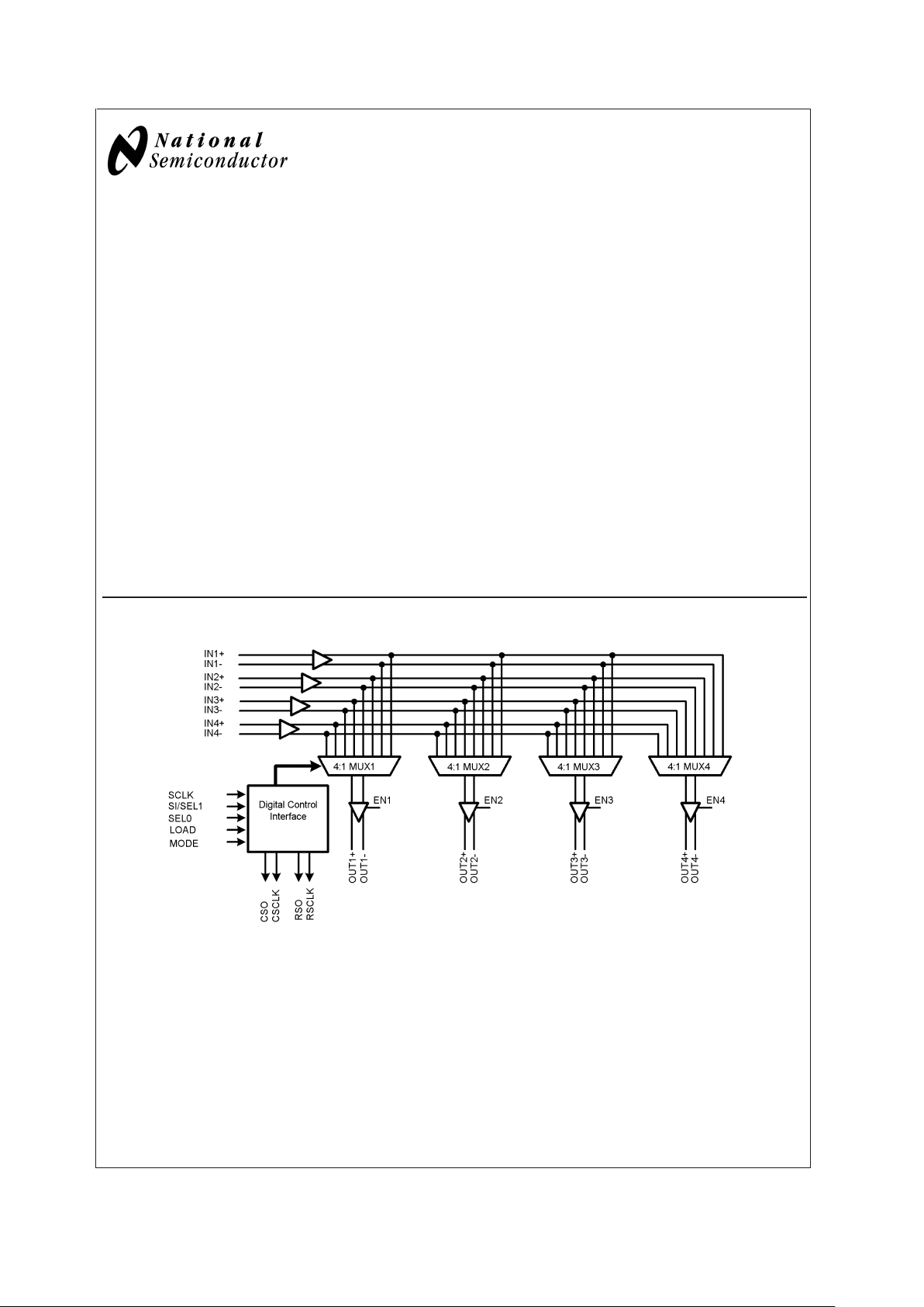
DS90CP04 is a 4x4 digital cross-point switch with broadside
input and output pins for efficient board layout. It utilizes Low
Voltage Differential Swing (LVDS) technology for low power,
high-speed operation. Data paths are fully differential from
input to output for low noise. The non-blocking architecture
allows connections of any input to any output or outputs. The
switch matrix consists of four differential 4:1 multiplexes.
Each output channel connects to one of the four inputs
common to all multiplexers. Each DS90CP04 output pair is
capable of independent operation up to 2.5Gb/s.
A simple serial control interface or a configuration select port
is activated by the state of the MODE pin. When utilizing the
serial control interface a single load command will update
the new switch configuration for all outputs simultaneously.
When the direct configuration port is used, output configurations are updated immediately based on the decoded
SEL0/1 logic state.
Features
n 2.5 Gbps fully differential data paths
n Non-blocking architecture
n Broadcast from any input
n Broadside pin-out
n Possible expansion to larger switch array
n Accepts LVDS/BLVDS/LVPECL/2.5V-CML inputs
n TRI-STATE LVDS outputs
n Serial control interface with read-back capability
n Double register loading
n Single +2.5V supply
n Low power, 575 mW Typ at 2.5 Gb/s
n Lead-less LLP-32 package 6x6 mm body size)
n Fabricated with advanced CMOS process technology
Functional Block Diagrams
20028701
April 2003
DS90CP04 4x4 Low Power 2.5 Gb/s LVDS Digital Cross-Point Switch
© 2003 National Semiconductor Corporation DS200287 www.national.com
Page 2
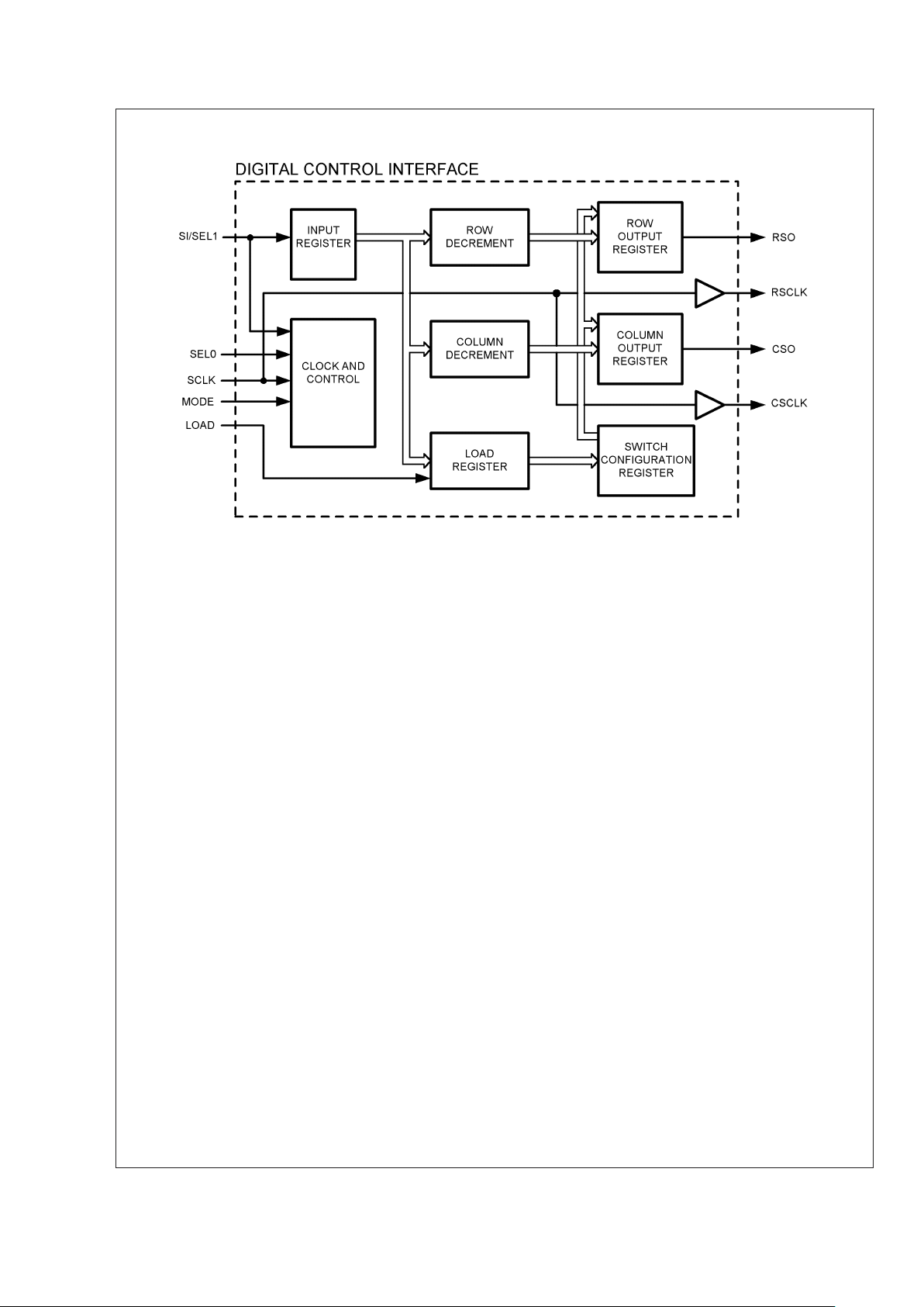
Functional Block Diagrams (Continued)
20028702
DS90CP04
www.national.com 2
Page 3
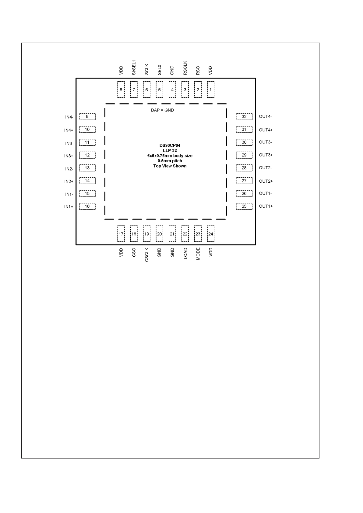
Connection Diagram
20028703
Order Number DS90CP04TLQ, DS90CP04TLQX (Tape and Reel)
See NS Package Number LQA32A
DS90CP04
www.national.com3
Page 4
Pin Descriptions
Pin
Name
Pin
Number
I/O, Type Description
DIFFERENTIAL INPUTS COMMON TO ALL MUXES
IN1+
IN1−
16
15
I, LVDS Inverting and non-inverting differential inputs.
IN2+
IN2−
14
13
I, LVDS Inverting and non-inverting differential inputs.
IN3+
IN3−
12
11
I, LVDS Inverting and non-inverting differential inputs.
IN4+
IN4−
10
9
I, LVDS Inverting and non-inverting differential inputs.
SWITCHED DIFFERENTIAL OUTPUTS
OUT1+
OUT1−
25
26
O, LVDS Inverting and non-inverting differential outputs. OUT1
±
can be connected to any
one pair IN1
±
, IN2±, IN3±,orIN4
±
OUT2+
OUT2−
27
28
O, LVDS Inverting and non-inverting differential outputs. OUT2±can be connected to any
one pair IN1
±
, IN2±, IN3±,orIN4
±
OUT3+
OUT3−
29
30
O, LVDS Inverting and non-inverting differential outputs. OUT3±can be connected to any
one pair IN1
±
, IN2±, IN3±,orIN4
OUT4+
OUT4−
31
32
O, LVDS Inverting and non-inverting differential outputs. OUT4
±
can be connected to any
one pair IN1
±
, IN2±, IN3±,orIN4
±
DIGITAL CONTROL INTERFACE
SCLK 6 I, LVCMOS Control clock to latch in programming data at SI. SCLK can be 0 MHz to
100 MHz. SCLK should be burst of clock pulses active only while accessing the
device. After completion of programming, SCLK should be kept at logic low to
minimize potential noise injection into the high-speed differential data paths.
SI / SEL1 7 I, LVCMOS Programming data to select the switch configuration. Data is latched into the input
buffer register at the rising edge of SCLK.
SEL0 5 I, LVCMOS Programming data to select the switch configuration.
CSO
RSO
18
2
O, LVCMOS With MODE low, control data is shifted out at CSO (RSO) for cascading to the
next device in the serial chain. The control data at CSO (RSO) is identical to that
shifted in at SI with the exception of the device column (row) address being
decremented by one internally before propagating to the next device in the chain.
CSO (RSO) is clocked out at the rising edge of SCLK.
CSCLK
RSCLK
19
3
O, LVCMOS With MODE low, these pins function as a buffered control clock from SCLK.
CSCLK (RSCLK) is used for cascading the serial control bus to the next device in
the serial chain.
LOAD 22 I, LVCMOS When LOAD is high and SCLK makes a LH transition, the device transfers the
programming data in the load register into the configuration registers. The new
switch configuration for all outputs takes effect. LOAD needs to remain high for
only one SCLK cycle to complete the process, holding LOAD high longer repeats
the transfer to the configuration register.
MODE 23 I, LVCMOS When MODE is low, the SCLK is active and a buffered SCLK signal is present at
the CLKOUT output. When MODE is high, the SCLK signal is uncoupled from
register and state machine internals. Internal registers will see an active low signal
until MODE is brought Low again.
POWER
V
DD
1, 8, 17,
24
I, Power VDD= 2.5V±5%. At least 4 low ESR 0.01 µF bypass capacitors should be
connected from V
DD
to GND plane.
GND 4, 20, 21,
DAP
I, Power Ground reference to LVDS and CMOS circuitry.
DAP is the exposed metal contact at the bottom of the LPP-32 package. The DAP
is used as the primary GND connection to the device. It should be connected to
the ground plane with at least 4 vias for optimal AC and thermal performance.
DS90CP04
www.national.com 4
Page 5
Serial Interface Truth Table
LOAD MODE SCLK Resulting Action
0 0 LH The current state on SI is clocked into the input shift register.
0 1 LH Uncouples SCLK input from register and state machine internals. Internal registers
will see and the RSCLK and CSCLK outputs will drive an active Low signal until
MODE is brought Low again. See Configuration Select Truth Table below.
LH 0 X Loads OUT1– OUT4 configuration information from last valid frame. Places contents
of load register into the configuration register. The switch configuration is updated
asynchronously from the SCLK input.
1 1 LH Uncouples SCLK input from register and state machine internals. Internal registers
will see and the RSCLK and CSCLK outputs will drive an active Low signal until
MODE is brought Low again. See Configuration Select Truth Table below.
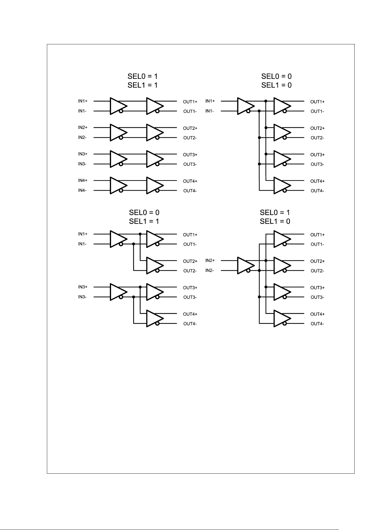
Configuration Select Truth Table
MODE SEL1 SEL0 Resulting Action
0 X X The SEL0/1 pins only function in configuration select mode. See below.
1 0 0 Distribution: IN1 - OUT1 OUT2 OUT3 OUT4
1 0 1 Distribution: IN2 - OUT1 OUT2 OUT3 OUT4
1 1 0 Redundancy: IN1 - OUT1 OUT2 and IN3 - OUT3 OUT4
1 1 1 Broadside: IN1 - OUT1, IN2 - OUT2, IN3 - OUT3, IN4 - OUT4
LH: Low to High (positive edge) transition.
X: Don’t Care or Not Applicable.
DS90CP04
www.national.com5
Page 6
Configuration Select Truth Table (Continued)
20028704
FIGURE 1. DS90CP04 Configuration Select Decode
DS90CP04
www.national.com 6
Page 7

Absolute Maximum Ratings (Note 1)
If Military/Aerospace specified devices are required,
please contact the National Semiconductor Sales Office/
Distributors for availability and specifications.
Supply Voltage (V
DD
) −0.3V to +3V
CMOS/TTL Input Voltage −0.3V to (V
DD
+0.3V)
LVDS Receiver Input Voltage −0.3V to +3.3V
LVDS Driver Output Voltage −0.3V to +3V
LVDS Output Short Circuit Current 40mA
Junction Temperature +150˚C
Storage Temperature −65˚C to +150˚C
Lead Temperature
(Soldering, 4 sec.) +260˚C
Maximum Package Power Dissipation at 25˚C
LLP-32 3200 mW
Derating above 25˚C 38 mW/˚C
Thermal Resistance, θ
JA
26.4˚C/W
ESD Rating
HBM, 1.5 kΩ, 100 pF
LVDS Outputs
>
1.0 kV
LVDS Inputs
>
1.5 kV
All Other Pins
>
4.0 kV
EIAJ, 0Ω, 200 pF
>
100V
Recommended Operating
Conditions
Min Typ Max Unit
Supply Voltage (V
DD
– GND) 2.375 2.5 2.625 V
Receiver Input Voltage 0.05 3.3 V
Operating Free Air
Temperature −40 25 85 ˚C
Junction Temperature 110 ˚C
Electrical Characteristics
Over recommended operating supply and temperature ranges unless other specified.
Symbol Parameter Conditions Min
Typ (Note
2)
Max Units
LVCMOS/LVTTL DC SPECIFICATIONS (SCLK, SI/SEL1, SEL0, LOAD, MODE , CSCLK, RSCLK, CSO, RSO)
V
IH
High Level Input Voltage 1.7 V
DD
V
V
IL
Low Level Input Voltage GND 0.7 V
I
IH
High Level Input Current VIN=VDD=V
DDMAX
−10 +10 µA
I
IL
Low Level Input Current VIN=VSS,VDD=V
DDMAX
−10 +10 µA
C
IN1
Input Capacitance Any Digital Input Pin to V
SS
3.5 pF
C
OUT1
Output Capacitance Any Digital Output Pin to V
SS
5.5 pF
V
CL
Input Clamp Voltage ICL= −18 mA −1.5 −0.8 V
V
OH
High Level Output Voltage IOH= −4.0 mA, VDD=V
DDMIN
1.9 V
I
OH
= −100 µA, VDD= 2.5V 2.4 V
V
OL
Low Level Output Voltage IOL= 4.0 mA, VDD=V
DDMIN
0.4 V
I
OL
= 100 µA, VDD= 2.5V 0.1 V
LVDS INPUT DC SPECIFICATIONS (IN1
±
, IN2±, IN3±, IN4±)
V
TH
Differential Input High Threshold
(Note 3)
VCM= 0.05V or 1.2V or 2.45V,
V
DD
= 2.5V
050mV
V
TL
Differential Input Low Threshold VCM= 0.05V or 1.2V or 2.45V,
V
DD
= 2.5V
−50 0 mV
V
ID
Differential Input Voltage VDD= 2.5V, VCM= 0.05V to 2.45V 100 V
DD
mV
V
CMR
Common Mode Voltage Range VID= 100 mV, VDD= 2.5V 0.05 3.25 V
C
IN2
Input Capacitance IN+ or IN− to V
SS
3.5 pF
I
IN
Input Current VIN= 2.5V, VDD=V
DDMAX
or 0V −10 +10 µA
V
IN
= 0V, VDD=V
DDMAX
or 0V −10 +10 µA
LVDS OUTPUT DC SPECIFICATIONS (OUT1
±
, OUT2±, OUT3±, OUT4±)
V
OD
Differential Output Voltage (Note3)RL= 100Ω between OUT+ and
OUT−Figure 2
250 400 475 mV
∆V
OD
Change in VODbetween
Complementary States
−35 35 mV
V
OS
Offset Voltage (Note 4) 1.125 1.25 1.375 V
∆V
OS
Change in VOSbetween
Complementary States
−35 35 mV
DS90CP04
www.national.com7
Page 8

Electrical Characteristics (Continued)
Over recommended operating supply and temperature ranges unless other specified.
Symbol Parameter Conditions Min
Typ (Note
2)
Max Units
I
OZ
Output TRI-STATE Current TRI-STATE Output
V
OUT=VDD
or V
SS
−10 +10 µA
I
OFF
Power Off Leakage Current VDD= 0V, V
OUT
= 2.5V or GND −10 +10 µA
I
OS
Output Short Circuit Current,
One Complementary Output
OUT+ or OUT− Short to GND −15 -40 mA
OUT+ or OUT− Short to V
DD
15 40 mA
I
OSB
Output Short Circuit Current,
both Complementary Outputs
OUT+ and OUT− Short to GND −15 -30 mA
OUT+ and OUT− Short to V
CM
15 30 mA
C
OUT2
Output Capacitance OUT+ or OUT− to GND when
TRI-STATE
5.5 pF
SUPPLY CURRENT
I
CCD
Total Supply Current All inputs and outputs enabled,
terminated with differential load of
100Ω between OUT+ and OUT-.
220 300 mA
I
CCZ
TRI-STATE Supply Current TRI-STATE All Outputs 10 20 mA
SWITCHING CHARACTERISTICS — LVDS OUTPUTS (Figures 3, 5, 6)
t
LHT
Differential Low to High
Transition Time
Use an alternating 1 and 0 pattern
at 200 Mb/s, measure between
20% and 80% of V
OD
.
100 135 160 ps
t
HLT
Differential High to Low
Transition Time
100 135 160 ps
t
PLHD
Differential Low to High
Propagation Delay
Use an alternating 1 and 0 pattern
at 200 Mb/s, measure at 50% V
OD
between input to output.
500 750 1200 ps
t
PHLD
Differential High to Low
Propagation Delay
500 750 1200 ps
t
SKD1
Pulse Skew |t
PLHD–tPHLD
| 0 30 ps
t
SKCC
Output Channel to Channel
Skew
Difference in propagation delay
(t
PLHD
or t
PHLD
) among all output
channels in Broadcast mode (any
one input to all outputs).
0 50 100 ps
t
JIT
Jitter (Note 5)
Alternating 1 and 0 Pattern
750 MHz 1.6 2.5 psrms
1.25 GHz 1.6 2.5 psrms
K28.5 Pattern
1.5 Gb/s 10 40 psp-p
2.5 Gb/s 27 60 psp-p
PRBS 2
23
-1 Pattern
1.5 Gb/s 25 40 psp-p
2.5 Gb/s 40 70 psp-p
t
ON
LVDS Output Enable Time Time from LOAD = LH or SELx to
OUT
±
change from TRI-STATE to
active.
50 150 300 ns
t
OFF
LVDS Output Disable Time Time from LOAD = LH or SELx to
OUT
±
change from active to
TRI-STATE.
35ns
t
SW
LVDS Switching Time Time from LOAD = LH to new
switch configuration effective for
OUT
±
.
50 150 ns
DS90CP04
www.national.com 8
Page 9

Electrical Characteristics (Continued)
Over recommended operating supply and temperature ranges unless other specified.
Symbol Parameter Conditions Min
Typ (Note
2)
Max Units
t
SEL
SELx to OUT
±
Configuration select to new data at
OUT
±
.
50 150 ns
SWITCHING CHARACTERISTICS — Serial control Interface (Figures 4, 8, 9)
F
SCLK
SCLK Clock Frequency 0 100 MHz
T
DCCLK
CSCLK Duty Cycle
RSCLK Duty Cycle
Input SCLK Duty Cycle set at 50%
45 55 %
t
S
SI–SCLK or MODE–SCLK
Setup Time
From SI or MODE Input Data to
SCLK Rising Edge
1.5 ns
t
H
SCLK–SI or SCLK–MODE Hold
Time
From SCLK Rising Edge to SI or
MODE Input Data
1ns
t
DSO
SCLK to RSO or CSO Delay From SCLK to RSO or CSO 1.5 4 ns
t
DSCLK
SCLK to RSCLK or CSCLK
Delay
From SCLK to RSCLK or CSCLK
4.0 8.5 ns
t
DSDIF
|SCLK to RSCLK or
CSCLK–SCLK to RSO or CSO|
Propagation Delay Difference
between t
DSO
and t
DSCLK
1.5 4.5 ns
T
RISE
Logic Low to High Transition
Time
20% to 80% at RSO, CSO,
RSCLK, or CSCLK
1.5 ns
T
FALL
Logic High to Low Transition
Time
80% to 20% at RSO, CSO,
RSCLK, or CSCLK
1.5 ns
Note 1: “Absolute Maximum Ratings” are the ratings beyond which the safety of the device cannot be guaranteed. They are not meant to imply that the device
should be operated at these limits.
Note 2: Typical parameters are measured at V
DD
= 2.5V, TA= 25˚C. They are for reference purposes, and are not production-tested.
Note 3: Differential output voltage V
OD
is defined as |OUT+–OUT−|. Differential input voltage VIDis defined as |IN+–IN−|.
Note 4: Output offset voltage V
OS
is defined as the average of the LVDS single-ended output voltages at logic high and logic low states.
Note 5: Characterized from any input to any one differential LVDS output running at the specified data rate and data pattern, with all other 3 channels running K28.5
pattern at 1.25 Gb/s asynchronously to the channel under test. Jitter is not production-tested, but guaranteed through characterization on sample basis. Random
Jitter is measured peak to peak with a histogram including 1000 histogram window hits. K28.5 pattern is repeating bit streams of (0011111010 1100000101). This
deterministic jitter or DJ pattern is measured to a histogram mean with a sample size of 350 hits. Like RJ the Total Jitter or TJ is measured peak to peak with a
histogram including 3500 window hits.
20028712
FIGURE 2. Differential Driver DC Test Circuit
DS90CP04
www.national.com9
Page 10

Electrical Characteristics (Continued)
20028713
FIGURE 3. Differential Driver AC Test Circuit
20028714
FIGURE 4. LVCMOS Driver AC Test Circuit (Note 6)
DS90CP04
www.national.com 10
Page 11

Electrical Characteristics (Continued)
Note 6: The LVCMOS input and output AC specifications may also be verified and tested using an input attenuation network instead of a power splitter as shown
in Figure 4.
20028715
FIGURE 5. LVDS Signals
20028716
FIGURE 6. LVDS Output Transition Time
20028717
FIGURE 7. LVDS Output Propagation Delay
DS90CP04
www.national.com11
Page 12

20028718
FIGURE 8. Serial Interface Propagation Delay and Input Timing Waveforms
20028719
FIGURE 9. Serial Interface — MODE Timing and Functionality
DS90CP04
www.national.com 12
Page 13

Functional Descriptions
PROGRAMMING WITH THE SERIAL INTERFACE
The configuration of the internal multiplexer is programmed
through a simple serial interface consisting of serial clock
SCLK and serial input data line SI. The serial interface is
designed for easy expansion to larger switch array. A replicated output serial interface (RSCLK, RSO) is provided for
propagating the control data to the downstream device in the
row of an array of DS90CP04 devices in a matrix. A similar
replicated serial interface (CSCLK, CSO) is provided for
propagating the control data to the downstream devices in
the first column of the device matrix. Through this scheme,
user can program all the devices in the matrix through one
serial control bus (SCLK and SI) with the use of the feedthrough replicated control bus at RSCLK and RSO, CSCLK
and CSO.
To program the configuration of the switch, a 30-bit control
word is sent to the device. The first 6 bits shift the start frame
into SI. The only two valid start frames are 1F’h for a configuration load and 1E’h for a configuration read. The start
frame is followed by the row and column addresses of the
device to be accessed, as well as the switch configuration of
the four channels of the device. Table 1 and Table 2 are the
bit definitions of the control word. D29 is the first bit that
shifts into SI.
TABLE 1. 30-Bit Control Word
Bit Bit Length Descriptions
D29–D24 6 The start frame for control word synchronization (01 1111’b = LOAD).
D23–D18 6 Specify the row address of the device to be access. The serial interface can access up to 64
devices in the row.
D17–D12 6 Specify the column address of the device to be access. The serial interface can access up to 64
devices in the column.
D11–D9 3 Specify the switch configuration for Output 1. See Table 2.
D8–D6 3 Specify the switch configuration for Output 2. See Table 2.
D5–D3 3 Specify the switch configuration for Output 3. See Table 2.
D2–D0 3 Specify the switch configuration for Output 4. See Table 2.
TABLE 2. Switch Configuration Data
MSB LSB OUT1±Connects to OUT2±Connects to OUT3±Connects to OUT4±Connects to
0 0 0 Output 1 Tri-Stated Output 2 Tri-Stated Output 3 Tri-Stated Output 4 Tri-Stated
001IN1
±
IN1
±
IN1
±
IN1
±
010IN2
±
IN2
±
IN2
±
IN2
±
011IN3
±
IN3
±
IN3
±
IN3
±
100IN4
±
IN4
±
IN4
±
IN4
±
1 0 1 Invalid.
20028720
FIGURE 10. Configuration and Output Enable/Disable Timing
DS90CP04
www.national.com13
Page 14

Functional Descriptions (Continued)
TABLE 2. Switch Configuration Data (Continued)
MSB LSB OUT1±Connects to OUT2±Connects to OUT3±Connects to OUT4±Connects to
1 1 0 Use of these invalid combinations may cause loss of synchronization.
111
ROW AND COLUMN ADDRESSING
The upper left device in an array of NxN devices is assigned
row address 0, and column address 0. The devices to its
right have column addresses of 1 to N, whereas devices
below it have row addresses of 1 to N. The Serial Control
Interface (SCLK and SI) is connected to the first device with
the row and column addresses of 0. The Serial Control
Interface shifts in a control word containing the row and
column address of the device it wants to access. When the
control data propagates through each device, the control
word’s address is internally decremented by one before it is
sent to the next row or column device. When the control data
is sent out the column interface (CSO and CSCLK) the row
address is decremented by one. Similarly, when the column
address data is shifted out the row interface (RSO and
RSCLK) the column address is decremented by one. By the
time the control word reaches the device it has been intended to program, both the row and column addresses
have been decremented to 0.
Each device constantly checks for the receipt of a frame start
(D29-24=01 1111’b or 01 1110’b). When it detects the proper
start frame string, and the row and column addresses it
receives are both 0, the device responds by storing the
switch configuration data of the 30-bit control word into its
load register.
Each device in the array is sequentially programmed through
the serial interface. When programming is completed for the
entire array, LOAD is pulsed high and the load register’s
content is transferred to the configuration register of each
device. The LOAD pulse must wait until the final bit of the
control word has been placed into the "load" register. This
timing is guaranteed to take place two clock cycles after
programming has been completed.
Due to internal shift registers additional SCLK cycles will be
necessary to complete array programming. It takes 7 clock
(SCLK) positive edge transitions for the control data to appear at RSO and CSO for its near neighbor. Users must
provide the correct number of clock transitions for the control
data word to reach its destination in the array. Table 3 shows
an example of the control data words for a 4 device serial
chain with connections (OUT1=IN1, OUT2=IN2,
OUT16=IN16). To program the array, it requires four 30-bit
control words to ripple through the serial chain and reach
their destinations. In order to completely program the array
in the 120 clock cycles associated with the 30-bit control
words it is important to program the last device in the chain
first. The following programming data pushes the initial data
through the chain into the correct devices.
READ-BACK SWITCH CONFIGURATION
The DS90CP04 is put into read-back mode by sending a
special “Read” start frame (01 1110’b). Upon receipt of the
special read start frame the configuration register information is transferred into the shift register and output at both
RSO and CSO in the OUT1 to OUT4 bit segments of the
read control word. Each time the read-back data from a
device passes through its downstream device, its default
address (11 1111’b) is internally decremented by one. The
“relative” column address emerges at RSO of the last device
in the row and is used to determine (11 1111’b - N) the
column of the sending device. Similarly, the row address
emerges at CSO of the sending device. After inserting the
channel configuration information in the “read” control word,
the device will automatically revert to write mode, ready to
accept a new control word at SI.
Table 4 shows an example of reading back the configuration
registers of 4 devices in the first row of a 4x4 device array.
Again, due to internal shift registers additional SCLK cycles
will be necessary to complete the array read. It takes 4x30
SCLK clock cycles to shift out 4 30-bit configuration registers
plus 7 SCLK cycles per device to account for device latency
making for a total SCLK count of 148. The serialized read
data is sampled at RSO and synchronized with RSCLK of
the last device in the row. The user is recommended to
backfill with all 0’s at SI after the four reads have been
shifted in.
TABLE 3. Example to Program a 4 Device Array
Frame
D29:D24
Row
Address
D23:D18
Column
Address
D17:D12
OUT1
D11:D9
OUT2
D8:D6
OUT3
D5:D3
OUT4
D2:D0
Number of
SCLK
Cycles
Control Word
Destination
Device in
Array
Row, Column
01 1111 00 0000 00 0011 001 010 011 100 30 0, 3
01 1111 00 0000 00 0010 001 010 011 100 30 0, 2
01 1111 00 0000 00 0001 001 010 011 100 30 0, 1
01 1111 00 0000 00 0000 001 010 011 100 30 0, 0
Shift in configuration information from device furthest from system SI input first to minimize array
latency during the programming process.
The 2 clock cycle delay ensures all channel information has reached the “load” register and all
switches are ready to be configured.
2
DS90CP04
www.national.com 14
Page 15

Functional Descriptions (Continued)
TABLE 4. A Read-Back Example from a 4 Device Array
Frame
D29:D24
Row
Address
D23:D18
Column
Address
D17:D12
OUT1
D11:D9
OUT2
D8:D6
OUT3
D5:D3
OUT4
D2:D0
Number of
SCLK
Cycles
Descriptions
01 1110 00 0000 11 1111 0 00 00 0 000 00 0 30
Read-Back
(R,C)=0, 3
01 1110 00 0000 11 1110 000 000 000 000 30
Read-Back
(R,C)=0, 2
01 1110 00 0000 11 1101 000 000 000 000 30
Read-Back
(R,C)=0, 1
01 1110 00 0000 11 1100 001 010 011 100 30
Read-Back
(R,C)=0, 0
Note 7: LOAD and READ programming example is based on the 16x16 array configuration shown in Figure 11. Alternative expansion array configurations will
require a slightly different programming sequence.
SWITCH EXPANSION FOR MINIMUM PROGRAMMING
LATENCY
Programming data ripples through the array through RSO
and RSCLK in the row and CSO and CSCLK in the first
column. LOAD pins of all devices are electrically tied to-
gether and driven by the same “load” signal. To prevent
excessive stub length in the array from affecting the signal
quality of LOAD, it is recommended that the load signal is
distributed to each row or column in large crosspoint array
applications.
20028707
FIGURE 11.
DS90CP04
www.national.com15
Page 16

Programming Example
CONFIGURATION WRITE
30 Bit Control Word: [WRITE FRAME] [ROW ADDRESS][COLUMN ADDRESS] [OUT1][OUT2][OUT3][OUT4]
ARRAY WRITE:
[0 1 1111 ] [0][1] [1][1][1][1] //
*
Array position 1, Broadcast IN1*//
[0 1 1111 ] [0][0] [2][2][4][4] //
*
Array position 0, Connect IN2 to OUT1 and 2, IN4 to OUT3 and OUT4*//
LOAD = H and SCLK = LH
20028710
DEVICE 0 WRITE PROGRAMMING SEQUENCE
SCLK
Number
Event Description
6 Device 0 (R=0, C=0) detects “WRITE” frame of first Control Word.
18 Device 0 (R=0, C=0) sees Row = 1, Column = 0 of first Control Word. The Row address of the first Control
Word is decremented by 1 (Row Address = 0) and sent out RSO.
36 Device 0 (R=0, C=0) detects “WRITE” frame of second Control Word.
48 Device 0 (R=0, C=0) sees Row = 0, Column = 0 of second Control Word. This is a valid configuration write
address, Device 1 prepares to receive configuration information.
60 Device 0 (R=0, C=0) has received configuration information and is waiting for a LOAD.
DEVICE 1 WRITE PROGRAMMING SEQUENCE
SCLK
Number
Event Description
13 Device 1 (R=1, C=0) detects “WRITE” frame of first Control Word.
25 Device 1 (R=1,C=0) sees Row = 0, Column=0offirst Control Word. This is a valid configuration write
address, Device 1 prepares to receive configuration information.
37 Device 1 (R=1,C=0) has received configuration information and is waiting for a LOAD.
43 Device 1 (R=1, C=0) detects “WRITE” frame of second Control Word.
55 Device 1 (R=1,C=0) sees Row = 3F, Column=0ofsecond Control Word. The Row address of the second
Control Word is decremented by 1 (Row Address = 3E) and sent out RSO.
CONFIGURATION READ
30 Bit Control Word: [READ FRAME] [ROW ADDRESS][COLUMN ADDRESS] [OUT1][OUT2][OUT3][OUT4]
ARRAY WRITE:
[01 1110] [1][0] [0][0][0][0] //
*
Array position 1, Return Configuration Information*//
[01 1110] [0][0] [0][0][0][0] //
*
Array position 0, Return Configuration Information*//
DS90CP04
www.national.com 16
Page 17

Programming Example (Continued)
20028711
DEVICE 0 READ PROGRAMMING SEQUENCE
SCLK
Number
Event Description
6 Device 0 (R=0, C=0) detects “READ” frame of first Control Word.
18 Device 0 (R=0,C=0) sees Row = 1, Column=0offirst Control Word. The Row address of the first Control
Word is decremented by 1 (Row Address = 0) and sent out RSO.
36 Device 0 (R=0,C=0) detects "READ" frame of second Control Word.
48 Device 0 (R=0,C=0) sees Row = 0, Column=0ofsecond Control Word. This is a valid configuration read
address, Device 0 prepares to transmit configuration information. The Row address of the last Control Word is
decremented by 1 (Row Address = 3F) and sent out RSO.
60 Device 0 (R=0,C=0) has transmitted configuration information.
74 Finished transmitting configuration information at Array Output (RSO of Device 1).
DEVICE 1 READ PROGRAMMING SEQUENCE
SCLK
Number
Event Description
13 Device 1 (R=1, C=0) detects “READ” frame of first Control Word.
25 Device 1 (R=1,C=0) sees Row = 0, Column=0offirst Control Word. This is a valid configuration read
address, Device 1 prepares to transmit configuration information. The Row address of the last Control Word is
decremented by 1 (Row Address = 3F) and sent out RSO.
37 Device 1 (R=1,C=0) has transmitted configuration information at Array Output (RSO of Device 1).
DS90CP04
www.national.com17
Page 18

Physical Dimensions inches (millimeters) unless otherwise noted
LLP, Plastic, QUAD,
Order Number DS90CP04TLQ, DS90CP04TLQX (Tape and Reel)
NS Package Number LQA032A
LIFE SUPPORT POLICY
NATIONAL’S PRODUCTS ARE NOT AUTHORIZED FOR USE AS CRITICAL COMPONENTS IN LIFE SUPPORT
DEVICES OR SYSTEMS WITHOUT THE EXPRESS WRITTEN APPROVAL OF THE PRESIDENT AND GENERAL
COUNSEL OF NATIONAL SEMICONDUCTOR CORPORATION. As used herein:
1. Life support devices or systems are devices or
systems which, (a) are intended for surgical implant
into the body, or (b) support or sustain life, and
whose failure to perform when properly used in
accordance with instructions for use provided in the
labeling, can be reasonably expected to result in a
significant injury to the user.
2. A critical component is any component of a life
support device or system whose failure to perform
can be reasonably expected to cause the failure of
the life support device or system, or to affect its
safety or effectiveness.
National Semiconductor
Americas Customer
Support Center
Email: new.feedback@nsc.com
Tel: 1-800-272-9959
National Semiconductor
Europe Customer Support Center
Fax: +49 (0) 180-530 85 86
Email: europe.support@nsc.com
Deutsch Tel: +49 (0) 69 9508 6208
English Tel: +44 (0) 870 24 0 2171
Français Tel: +33 (0) 1 41 91 8790
National Semiconductor
Asia Pacific Customer
Support Center
Email: ap.support@nsc.com
National Semiconductor
Japan Customer Support Center
Fax: 81-3-5639-7507
Email: jpn.feedback@nsc.com
Tel: 81-3-5639-7560
www.national.com
DS90CP04 4x4 Low Power 2.5 Gb/s LVDS Digital Cross-Point Switch
National does not assume any responsibility for use of any circuitry described, no circuit patent licenses are implied and National reserves the right at any time without notice to change said circuitry and specifications.
 Loading...