

Page 1
DS90C387/DS90CF388
Dual Pixel LVDS Display Interface (LDI)-SVGA/QXGA
General Description
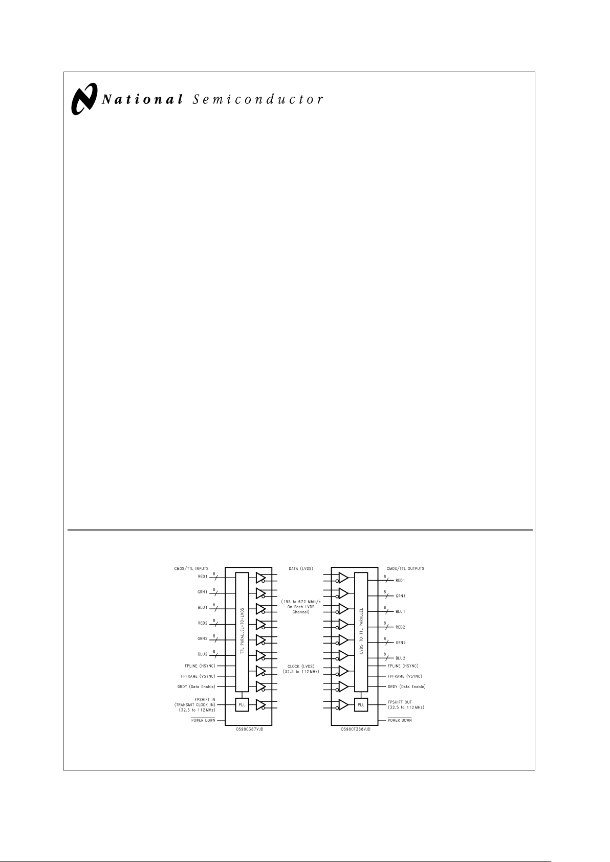
The DS90C387/DS90CF388 transmitter/receiver pair is designed to support dual pixel data transmission between Host
and Flat Panel Display up to QXGA resolutions. The transmitter converts 48bits(DualPixel 24-bit color) of CMOS/TTL
data into 8 LVDS (Low Voltage Differential Signalling) data
streams. Control signals (VSYNC, HSYNC, DE and two
user-defined signals) are sent during blanking intervals. At a
maximum dual pixel rate of 112MHz,LVDSdata line speed is
672Mbps, providing a total throughput of 5.38Gbps (672
Megabytes per second). Two other modes are also supported. 24-bit color data (single pixel) can be clocked into the
transmitter at a maximum rate of 170MHz. In this mode, the
transmitter provides single-to-dual pixel conversion, and the
output LVDS clock rate is 85MHz maximum. The third mode
provides inter-operability with FPD-Link devices.
The LDI chipset is improved over prior generations of
FPD-Link devices and offers higher bandwidth support and
longer cable drive with three areas of enhancement. To increase bandwidth, the maximum pixel clock rate is increased
to 112 (170) MHz and 8 serialized LVDS outputs are provided. Cable drive is enhanced with a user selectable
pre-emphasis feature that provides additional output current
during transitions to counteract cable loading effects. DC
balancing on a cycle-to-cycle basis, is also provided to reduce ISI (Inter-Symbol Interference). With pre-emphasis and
DC balancing, a low distortion eye-pattern is provided at the
receiver end of the cable. A cable deskew capability has
been added to deskew long cables of pair-to-pair skew of up
to +/−1 LVDSdata bit time. These three enhancements allow
cables 5 to 10+ meters in length to be driven.
This chipset is an ideal means to solve EMI and cable size
problems for high-resolution flat panel applications. It pro-
vides a reliable interface based on LVDS technology that delivers the bandwidth needed for high-resolution panels while
maximizing bit times, and keeping clock rates low to reduce
EMI and shielding requirements. For more details, please refer to the “Applications Information” section of this datasheet.
Features
n Complies with OpenLDI specification for digital display
interfaces
n 32.5 to 112/170MHz clock support
n Supports SVGA through QXGA panel resolutions
n Drives long, low cost cables
n Up to 5.38Gbps bandwidth
n Pre-emphasis reduces cable loading effects
n DC balance data transmission provided by transmitter
reduces ISI distortion
n Deskews +/−1 LVDS data bit time of pair-to-pair skew at
receiver inputs; intra-pair skew tolerance of 300ps
n Dual pixel architecture supports interface to GUI and
timing controller; optional single pixel transmitter inputs
support single pixel GUI interface
n Transmitter rejects cycle-to-cycle jitter
n 5V tolerant on data and control input pins
n Programmable transmitter data and control strobe select
(rising or falling edge strobe)
n Backward compatible configuration select with FPD-Link
n Optional second LVDS clock for backward compatibility
w/ FPD-Link
n Support for two additional user-defined control signals in
DC Balanced mode
n Compatible with TIA/EIA - LVDS Standard
Generalized Block Diagram
TRI-STATE®is a registered trademark of National Semiconductor Corporation.
DS100073-1
PRELIMINARY
May 2000
DS90C387/DS90CF388 Dual Pixel LVDS Display Interface (LDI)-SVGA/QXGA
© 2000 National Semiconductor Corporation DS100073 www.national.com
Page 2
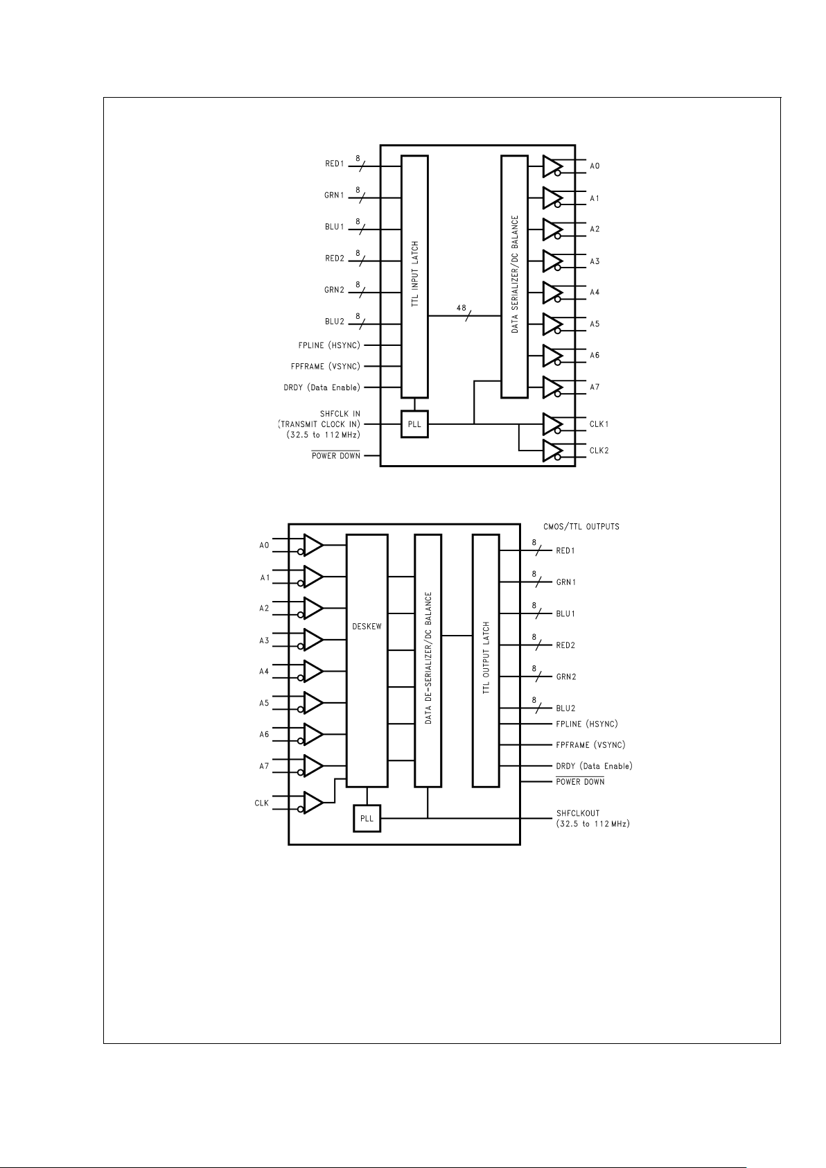
Transmitter Block Diagram
Receiver Block Diagram
DS100073-2
DS100073-3
DS90C387/DS90CF388
www.national.com 2
Page 3
Absolute Maximum Ratings (Note 1)
If Military/Aerospace specified devices are required,
please contact the National Semiconductor Sales Office/
Distributors for availability and specifications.
Supply Voltage (V
CC
) −0.3V to +4V
CMOS/TTL Input Voltage −0.3V to +5.5V
CMOS/TTL Output Voltage −0.3V to (V
CC
+ 0.3V)
LVDS Receiver Input
Voltage −0.3V to +3.6V
LVDS Driver Output
Voltage −0.3V to +3.6V
LVDS Output Short Circuit
Duration Continuous
Junction Temperature +150˚C
Storage Temperature −65˚C to +150˚C
Lead Temperature
(Soldering, 4 sec.) +260˚C
Maximum Package Power Dissipation Capacity
@
25˚C
100 TQFP Package:
DS90C387 2.8W
DS90CF388 2.8W
Package Derating:
DS90C387 18.2mW/˚C above +25˚C
DS90CF388 18.2mW/˚C above +25˚C
ESD Rating:
DS90C387
(HBM, 1.5kΩ, 100pF)
>
6kV
(EIAJ, 0Ω, 200pF)
>
300 V
DS90CF388
(HBM, 1.5kΩ, 100pF)
>
2kV
(EIAJ, 0Ω, 200pF)
>
200 V
Recommended Operating
Conditions
Min Nom Max Units
Supply Voltage (V
CC
) 3.0 3.3 3.6 V
Operating Free Air
Temperature (T
A)
−10 +25 +70 ˚C
Receiver Input Range 0 2.4 V
Supply Noise Voltage (V
CC
) 100 mV
p-p
Electrical Characteristics
Over recommended operating supply and temperature ranges unless otherwise specified.
Symbol Parameter Conditions Min Typ Max Units
CMOS/TTL DC SPECIFICATIONS (Tx inputs, Rx outputs, control inputs and outputs)
V
IH
High Level Input Voltage 2.0 V
CC
V
V
IL
Low Level Input Voltage GND 0.8 V
V
OH
High Level Output Voltage IOH= −0.4 mA 2.7 2.9 V
I
OH
= −2 mA 2.7 2.85 V
V
OL
Low Level Output Voltage IOL= 2 mA 0.1 0.3 V
V
CL
Input Clamp Voltage ICL= −18 mA −0.79 −1.5 V
I
IN
Input Current VIN= 0.4V, 2.5V or V
CC
+1.8 +15 µA
V
IN
= GND −15 0 µA
I
OS
Output Short Circuit Current V
OUT
= 0V −120 mA
LVDS DRIVER DC SPECIFICATIONS
V
OD
Differential Output Voltage RL= 100Ω 250 345 450 mV
∆V
OD
Change in VODbetween
Complimentary Output States
35 mV
V
OS
Offset Voltage 1.125 1.25 1.375 V
∆V
OS
Change in VOSbetween
Complimentary Output States
35 mV
I
OS
Output Short Circuit Current V
OUT
= 0V, RL= 100Ω −3.5 −10 mA
I
OZ
Output TRI-STATE®Current PD = 0V, V
OUT
=0VorV
CC
±
1
±
10 µA
LVDS RECEIVER DC SPECIFICATIONS
V
TH
Differential Input High
Threshold
VCM= +1.2V +100 mV
V
TL
Differential Input Low Threshold −100 mV
I
IN
Input Current VIN= +2.4V, VCC= 3.6V
±
10 µA
V
IN
= 0V, VCC= 3.6V
±
10 µA
DS90C387/DS90CF388
www.national.com3
Page 4
Electrical Characteristics (Continued)
Over recommended operating supply and temperature ranges unless otherwise specified.
Symbol Parameter Conditions Min Typ Max Units
TRANSMITTER SUPPLY CURRENT
ICCTW Transmitter Supply Current
Worst Case
R
L
= 100Ω,CL=
5 pF,
Worst Case
Pattern
(
Figures 1, 3
),
DUAL=High
(48-bit RGB),
BAL=High
(enabled)
f = 32.5 MHz 91.4 140 mA
f = 65 MHz 106 160 mA
f = 85 MHz 135 170 mA
f = 112 MHz 155 190 mA
ICCTG Transmitter Supply Current
16 Grayscale
R
L
= 100Ω,CL=
5 pF,
16 Grayscale
Pattern
(
Figures 2, 3
),
DUAL=High
(48-bit RGB),
BAL=High
(enabled)
f = 32.5 MHz 62.6 120 mA
f = 65 MHz 84.4 130 mA
f = 85 MHz 89.0 145 mA
f = 112 MHz 94.5 155 mA
ICCTZ Transmitter Supply Current
Power Down
PD = Low
4.8 50 µA
Driver Outputs in TRI-STATE under
Powerdown Mode
RECEIVER SUPPLY CURRENT
ICCRW Receiver Supply Current
Worst Case
C
L
= 8 pF,
Worst Case
Pattern
(
Figures 1, 4
),
DUAL (48-bit
RGB), BAL=High
(enabled)
f = 32.5 MHz 115 150 mA
f = 65 MHz 200 250 mA
f = 85 MHz 240 275 mA
f = 112 MHz 250 300 mA
ICCRG Receiver Support Current
16 Grayscale
C
L
= 8 pF,
16 Grayscale
Pattern
(
Figures 2, 4
),
DUAL (48-bit
RGB), BAL=High
(enabled)
f = 32.5 MHz 60 95 mA
f = 65 MHz 95 125 mA
f = 85 MHz 115 150 mA
f = 112 MHz 150 270 mA
ICCRZ Receiver Supply Current
Power Down
PD = Low
Receiver Outputs stay low
during Powerdown mode.
255 300 µA
Note 1: “Absolute Maximum Ratings” are those values beyond which the safety of the device cannot be guaranteed. They are not meant to imply that the device
should be operated at these limits. The tables of “Electrical Characteristics” specify conditions for device operation.
Note 2: Typical values are given for V
CC
= 3.3V and TA= +25˚C.
Note 3: Current into device pins is defined as positive. Current out of device pins is defined as negative. Voltages are referenced to ground unless otherwise specified (except V
OD
and ∆VOD).
DS90C387/DS90CF388
www.national.com 4
Page 5
Recommended Transmitter Input Characteristics
Over recommended operating supply and temperature ranges unless otherwise specified.
Symbol Parameter Min Typ Max Units
TCIT TxCLK IN Transition Time (
Figure 5
) DUAL=Gnd or Vcc 1.0 2.0 3.0 ns
DUAL=1/2Vcc 1.0 1.5 1.7 ns
TCIP TxCLK IN Period (
Figure 6
) DUAL=Gnd or Vcc 8.928 T 30.77 ns
DUAL=1/2Vcc 5.88 15.38 ns
TCIH TxCLK in High Time (
Figure 6
) 0.35T 0.5T 0.65T ns
TCIL TxCLK in Low Time (
Figure 6
) 0.35T 0.5T 0.65T ns
TXIT TxIN Transition Time 1.5 6.0 ns
Transmitter Switching Characteristics
Over recommended operating supply and temperature ranges unless otherwise specified.
Symbol Parameter Min Typ Max Units
LLHT LVDS Low-to-High Transition Time (
Figure 3
), PRE = 0.75V
(disabled)
0.14 0.7 ns
LVDS Low-to-High Transition Time (
Figure 3
), PRE = Vcc (max) 0.11 0.6 ns
LHLT LVDS High-to-Low Transition Time (
Figure 3
), PRE = 0.75V
(disabled)
0.16 0.8 ns
LVDS High-to-Low Transition Time (
Figure 3
), PRE = Vcc (max) 0.11 0.7 ns
TBIT Transmitter Output Bit Width DUAL=Gnd or Vcc 1/7 TCIP ns
DUAL=1/2Vcc 2/7 TCIP ns
TCCS TxOUT Channel to Channel Skew 100 ps
TSTC TxIN Setup to TxCLK IN (
Figure 6
) 2.7 ns
THTC TxIN Hold to TxCLK IN (
Figure 6
)0ns
TJCC Transmitter Jitter Cycle-to-cycle (
Figures
13, 14
) (Note 5), DUAL=Vcc
f = 112 MHz 85 100 ps
f = 85 MHz 60 75 ps
f = 65 MHz 70 80 ps
f = 56 MHz 100 120 ps
f = 32.5 MHz 75 110 ps
TPLLS Transmitter Phase Lock Loop Set (
Figure 8
)10ms
TPDD Transmitter Powerdown Delay (
Figure 10
) 100 ns
DS90C387/DS90CF388
www.national.com5
Page 6
Receiver Switching Characteristics
Over recommended operating supply and temperature ranges unless otherwise specified.
Symbol Parameter Min Typ Max Units
CLHT CMOS/TTL Low-to-High Transition Time (
Figure 4
), Rx data out 1.52 2.0 ns
CMOS/TTL Low-to-High Transition Time (
Figure 4
), Rx clock out 0.5 1.0 ns
CHLT CMOS/TTL High-to-Low Transition Time (
Figure 4
), Rx data out 1.7 2.0 ns
CMOS/TTL High-to-Low Transition Time (
Figure 4
), Rx clock out 0.5 1.0 ns
RCOP RxCLK OUT Period (
Figure 7
) 8.928 T 30.77 ns
RCOH RxCLK OUT High Time (
Figure 7
)(Note 4) f = 112 MHz 3.5 ns
f = 85 MHz 4.5 ns
RCOL RxCLK OUT Low Time (
Figure 7
)(Note 4) f = 112 MHz 3.5 ns
f = 85 MHz 4.5 ns
RSRC RxOUT Setup to RxCLK OUT (
Figure 7
)(Note 4) f = 112 MHz 2.4 ns
f = 85 MHz 3.0 ns
RHRC RxOUT Hold to RxCLK OUT (
Figure 7
)(Note 4) f = 112 MHz 3.4 ns
f = 85 MHz 4.75 ns
RPLLS Receiver Phase Lock Loop Set (
Figure 9
)10ms
RPDD Receiver Powerdown Delay (
Figure 11
)1µs
RSKM Receiver Skew Margin without Deskew (
Figure
12
) (Notes 4, 6)
f = 112 MHz 170 ps
Receiver Skew Margin with Deskew (Note 7) 1.27 ns
Receiver Skew Margin without Deskew (
Figure
12
) (Notes 4, 6)
f = 85 MHz 160 ps
Receiver Skew Margin with Deskew (Note 7) 1.68 ns
Note 4: TheMinimum and Maximum Limits are based on statistical analysis of the device performance over voltage and temperature ranges. This parameter is functionally tested on Automatic TestEquipment (ATE).ATE is limited to 85MHz. Asample of characterization parts have been bench tested at 112MHzto verify functional
performance.
Note 5: The limits are based on bench characterization of the device’s jitter response over the power supply voltage range. Output clock jitter is measured with a
cycle-to-cycle jitter of
±
3ns applied to the input clock signal while data inputs are switching (see figures 15 and 16). A jitter event of 3ns, represents worse case jump
in the clock edge from most graphics VGA chips currently available. This parameter is used when calculating system margin as described in AN-1059.
Note 6: Receiver Skew Margin is defined as the valid data sampling region at the receiver inputs. This margin takes into account transmitter output pulse positions
(min and max) and the receiver input setup and hold time (internal data sampling window - RSPOS). This margin allows for LVDS interconnect skew, inter-symbol
interference (both dependent on type/length of cable) and clock jitter.
RSKM ≥ cable skew (type, length) + source clock jitter (cycle to cycle).
Note 7: This limit is based on the capability of deskew circuitry. This margin allows for LVDS interconnect skew, inter-symbol interference (both dependent on type/
length of cable) and clock jitter. RSKM with deskew is
±
1 LVDS bit time (1/7th clock period) data to clock skew.
DS90C387/DS90CF388
www.national.com 6
Page 7
AC Timing Diagrams
Note 8: The worst case test pattern produces a maximum toggling of digital circuits, LVDS I/O and CMOS/TTL I/O.
Note 9: The 16 grayscale test pattern tests device power consumption for a “typical” LCD display pattern. The test pattern approximates signal switching needed
to produce groups of 16 vertical stripes across the display.
Note 10:
Figures 1, 2
show a falling edge data strobe (TxCLK IN/RxCLK OUT).
DS100073-10
FIGURE 1. “Worst Case” Test Pattern
DS100073-11
FIGURE 2. “16 Grayscale” Test Pattern (Notes 8, 9, 10)
DS90C387/DS90CF388
www.national.com7
Page 8
AC Timing Diagrams (Continued)
DS100073-12
FIGURE 3. DS90C387 (Transmitter) LVDS Output Load and Transition Times
DS100073-13
FIGURE 4. DS90CF388 (Receiver) CMOS/TTL Output Load and Transition Times
DS100073-14
FIGURE 5. DS90C387 (Transmitter) Input Clock Transition Time
DS100073-15
FIGURE 6. DS90C387 (Transmitter) Setup/Hold and High/Low Times (Falling Edge Strobe)
DS100073-16
FIGURE 7. DS90CF388 (Receiver) Setup/Hold and High/Low Times
DS90C387/DS90CF388
www.national.com 8
Page 9

AC Timing Diagrams (Continued)
DS100073-19
FIGURE 8. DS90C387 (Transmitter) Phase Lock Loop Set Time
DS100073-20
FIGURE 9. DS90CF388 (Receiver) Phase Lock Loop Set Time
DS90C387/DS90CF388
www.national.com9
Page 10

AC Timing Diagrams (Continued)
DS100073-21
FIGURE 10. Transmitter Power Down Delay
DS100073-22
FIGURE 11. Receiver Power Down Delay
DS100073-25
C—Setup and Hold Time (Internal data sampling window) defined by Rspos (receiver input strobe position) min and max
Tppos—Transmitter output pulse position (min and max)
RSKM = Cable Skew (type, length) + Source Clock Jitter (cycle to cycle) (Note 11) + ISI (Inter-symbol interference) (Note 12)
Cable Skew—typically 10 ps–40 ps per foot, media dependent
Note 11: Cycle-to-cycle jitter is less than 100 ps at 112 MHz
Note 12: ISI is dependent on interconnect length; may be zero
FIGURE 12. Receiver Skew Margin
DS90C387/DS90CF388
www.national.com 10
Page 11

AC Timing Diagrams (Continued)
DS100073-27
FIGURE 13. TJCC Test Setup - DS90C387
DS100073-28
FIGURE 14. Timing Diagram of the Input Cycle-to-Cycle Clock Jitter
DS90C387/DS90CF388
www.national.com11
Page 12

DS90C387 Pin Description—FPD Link Transmitter
Pin Name I/O No. Description
Rn, Gn, Bn,
DE, HSYNC,
VSYNC
I 51 TTL level input. This includes: 16 Red, 16 Green, 16 Blue, and 3 control
lines HSYNC, VSYNC, DE (Data Enable).(Note 13)
AnP O 8 Positive LVDS differential data output.
AnM O 8 Negative LVDS differential data output.
CLKIN I 1 TTL level clock input.
R_FB I 1 Programmable data strobe select. Rising data strobe edge selected when
input is high. (Note 13)
R_FDE I 1 Programmable control (DE) strobe select. Tied high for data active when
DE is high. (Note 13)
CLK1P O 1 Positive LVDS differential clock output.
CLK1M O 1 Negative LVDS differential clock output.
PD
I 1 TTL level input. Assertion (low input) tri-states the outputs, ensuring low
current at power down. (Note 13)
PLLSEL I 1 PLL range select. This pin must be tied to Vcc. No connect or tied to Gnd
is reserved for future use.(Note 13)
BAL I 1 Mode select for dc balanced (new) or non-dc balanced (backward
compatible) interface. DC balance is active when input is high. (Note 13)
PRE I 1 Pre-emphasis level select. Pre-emphasis is active when input is tied to V
CC
through external pull-up resistor. Resistor value determines pre-emphasis
level (see table in application section). For normal LVDS drive level (No
pre-emphasis) leave this pin open (do not tie to ground).(Note 13)
DUAL I 1 Three-mode select for dual pixel, single pixel, or single pixel input to dual
pixel output operation. Single pixel mode when input is low (only LVDS
channels A0 thru A3 and CLK1 are active) for power savings. Dual mode is
active when input is high. Single in - dual out when input is at 1/2 Vcc.
(Note 13)
Figure 15
V
CC
I 4 Power supply pins for TTL inputs and digital circuitry.
GND I 5 Ground pins for TTL inputs and digital circuitry.
PLLV
CC
I 2 Power supply pin for PLL circuitry.
PLLGND I 3 Ground pins for PLL circuitry.
LVDSV
CC
I 3 Power supply pin for LVDS outputs.
LVDSGND I 4 Ground pins for LVDS outputs.
CLK2P/NC O 1 Additional positive LVDS differential clock output. Identical to CLK1P. No
connect if not used.
CLK2M/NC O 1 Additional negative LVDS differential clock output. Identical to CLK1M. No
connect if not used.
Note 13: Inputs default to “low” when left open due to internal pull-down resistor.
DS90C387/DS90CF388
www.national.com 12
Page 13

DS90CF388 Pin Description—FPD Link Receiver
Pin Name I/O No. Description
AnP I 8 Positive LVDS differential data inputs.
AnM I 8 Negative LVDS differential data inputs.
Rn, Gn, Bn,
DE, HSYNC,
VSYNC
O 51 TTL level data outputs. This includes: 16 Red, 16 Green, 16 Blue, and 3
control lines— HSYNC (LP), VSYNC (FLM), DE (Data Enable).
RxCLK INP I 1 Positive LVDS differential clock input.
RxCLK INM I 1 Negative LVDS differential clock input.
RxCLK OUT O 1 TTL level clock output. The falling edge acts as data strobe.
R_FDE I 1 Programmable control (DE) strobe select. Tied high for data active when
DE is high. (Note 13)
PLLSEL I 1 PLL range select. This pin must be tied to Vcc. No connect or tied to Gnd
is reserved for future use. (Note 13)
BAL I 1 Mode select for dc balanced (new) or non-dc balanced (backward
compatible) interface. BAL = LOW for non-DC Balanced mode. BAL =
HIGH for DC Balanced Mode (Auto-detect mode), with this pin HIGH the
received LVDS clock signal is used to determine if the interface is in new
or backward compatible mode. (Note 13)
DESKEW I 1 Deskew and oversampling “on/off” select. Deskew is active when input is
high. Only supported in DC balance mode (BAL=High). To complete the
deskew operation, a minimum of four clock cycles is required during
blanking time. (Note 13)
PD
I 1 TTL level input. When asserted (low input) the receiver data outputs are
low and clock output is high. (Note 13)
STOPCLK O 1 Indicates receiver clock input signal is not present with a logic high. With a
clock input present, a low logic is indicated.
V
CC
I 6 Power supply pins for TTL outputs and digital circuitry.
GND I 8 Ground pins for TTL outputs and digital circuitry
PLLV
CC
I 1 Power supply for PLL circuitry.
PLLGND I 2 Ground pin for PLL circuitry.
LVDSV
CC
I 2 Power supply pin for LVDS inputs.
LVDSGND I 3 Ground pins for LVDS inputs.
CNTLE,
CNTLF
O 2 TTL level data outputs. User-defined control signals - no connect when not
used.
Note 14: These receivers have input fail-safe bias circuitry to guarantee a stable receiver output for floating or terminated receiver inputs. Under test conditions receiver inputs will be in a HIGH state. If the clock input is floating/terminated, outputs will remain in the last valid state.
DS100073-8
FIGURE 15. Resistor Network for “DUAL” pin input - recommend using R1=R2=10kΩ for single to dual mode
DS90C387/DS90CF388
www.national.com13
Page 14

LVDS Interface
Different Color Mapping options exists. Please see National
Application Notes 1127 andAN-1163 for details. A careful review of Color Mapping information is recommended as there
is not a standardized color naming convention between 6-bit
and 8-bit color data with regards to LSB and MSB
designations.
TABLE 1. LVDS data bit naming convention
X Y Z Description
X=R Red
X=G Green
X=B Blue
Y=1 Odd (First) Pixel
Y=2 Even (Second) Pixel
Z=0-7 LVDS bit number (not VGA controller LSB to MSB)
Note 15: Fora 48-bit dual pixel application - LSB (Less Significant Bit) = R16,G16,B16,R26,G26,B26 and MSB (Most Significant Bit) = R15,G15,B15,R25,G25,B25.
Note 16: Fora 36-bit dual pixel application - LSB (Less Significant Bit) = R10,G10,B10,R20,G20,B20 and MSB (Most Significant Bit) = R15,G15,B15,R25,G25,B25.
TABLE 2. Single pixel per clock input application data mapping (DUAL=Gnd)
VGA - TFT Data Signals Color
Bits
Transmitter input pin names Receiver output pin names TFT Panel Data
Signals
24-bit 18-bit DS90C387 DS90CF388 18-bit 24-bit
LSB R0 R16 R16 R0
R1 R17 R17 R1
R2 R0 R10 R10 R0 R2
R3 R1 R11 R11 R1 R3
R4 R2 R12 R12 R2 R4
R5 R3 R13 R13 R3 R5
R6 R4 R14 R14 R4 R6
MSB R7 R5 R15 R15 R5 R7
LSB G0 G16 G16 G0
G1 G17 G17 G1
G2 G0 G10 G10 G0 G2
G3 G1 G11 G11 G1 G3
G4 G2 G12 G12 G2 G4
G5 G3 G13 G13 G3 G5
G6 G4 G14 G14 G4 G6
MSB G7 G5 G15 G15 G5 G7
LSB B0 B16 B16 B0
B1 B17 B17 B1
B2 B0 B10 B10 B0 B2
B3 B1 B11 B11 B1 B3
B4 B2 B12 B12 B2 B4
B5 B3 B13 B13 B3 B5
B6 B4 B14 B14 B4 B6
MSB B7 B5 B15 B15 B5 B7
TABLE 3. Dual pixel per clock input application data mapping (DUAL=Vcc)
VGA - TFT Data Signals Color
Bits
Transmitter input pin names Receiver output pin names TFT Panel Data
Signals
48-bit 36-bit DS90C387 DS90CF388 36-bit 48-bit
LSB RO0 R16 R16 RO0
RO1 R17 R17 RO1
RO2 RO0 R10 R10 RO0 RO2
DS90C387/DS90CF388
www.national.com 14
Page 15

LVDS Interface (Continued)
TABLE 3. Dual pixel per clock input application data mapping (DUAL=Vcc) (Continued)
VGA - TFT Data Signals Color
Bits
Transmitter input pin names Receiver output pin names TFT Panel Data
Signals
RO3 RO1 R11 R11 RO1 RO3
RO4 RO2 R12 R12 RO2 RO4
RO5 RO3 R13 R13 RO3 RO5
RO6 RO4 R14 R14 RO4 RO6
MSB RO7 RO5 R15 R15 RO5 RO7
LSB GO0 G16 G16 GO0
GO1 G17 G17 GO1
GO2 GO0 G10 G10 GO0 GO2
GO3 GO1 G11 G11 GO1 GO3
GO4 GO2 G12 G12 GO2 GO4
GO5 GO3 G13 G13 GO3 GO5
GO6 GO4 G14 G14 GO4 GO6
MSB GO7 GO5 G15 G15 GO5 GO7
LSB BO0 B16 B16 BO0
BO1 B17 B17 BO1
BO2 BO0 B10 B10 BO0 BO2
BO3 BO1 B11 B11 BO1 BO3
BO4 BO2 B12 B12 BO2 BO4
BO5 BO3 B13 B13 BO3 BO5
BO6 BO4 B14 B14 BO4 BO6
MSB BO7 BO5 B15 B15 BO5 BO7
LSB RE0 R26 R26 RE0
RE1 R27 R27 RE1
RE2 RE0 R20 R20 RE0 RE2
RE3 RE1 R21 R21 RE1 RE3
RE4 RE2 R22 R22 RE2 RE4
RE5 RE3 R23 R23 RE3 RE5
RE6 RE4 R24 R24 RE4 RE6
MSB RE7 RE5 R25 R25 RE5 RE7
LSB GE0 G26 G26 GE0
GE1 G27 G27 GE1
GE2 GE0 G20 G20 GE0 GE2
GE3 GE1 G21 G21 GE1 GE3
GE4 GE2 G22 G22 GE2 GE4
GE5 GE3 G23 G23 GE3 GE5
GE6 GE4 G24 G24 GE4 GE6
MSB GE7 GE5 G25 G25 GE5 GE7
LSB BE0 B26 B26 BE0
BE1 B27 B27 BE1
BE2 BE0 B20 B20 BE0 BE2
BE3 BE1 B21 B21 BE1 BE3
BE4 BE2 B22 B22 BE2 BE4
BE5 BE3 B23 B23 BE3 BE5
BE6 BE4 B24 B24 BE4 BE6
MSB BE7 BE5 B25 B25 BE5 BE7
DS90C387/DS90CF388
www.national.com15
Page 16

LVDS Interface (Continued)
TABLE 4. Single pixel per clock input-to-dual pixel per clock output data mapping (DUAL=1/2Vcc)
VGA - TFT Data Signals Color
Bits
Transmitter input pin names Receiver output pin names TFT Panel Data
Signals
24-bit 18-bit DS90C387 DS90CF388 36-bit 48-bit
LSB R0 R16 R16 RO0
R1 R17 R17 RO1
R2 R0 R10 R10 RO0 RO2
R3 R1 R11 R11 RO1 RO3
R4 R2 R12 R12 RO2 RO4
R5 R3 R13 R13 RO3 RO5
R6 R4 R14 R14 RO4 RO6
MSB R7 R5 R15 R15 RO5 RO7
LSB G0 G16 G16 GO0
G1 G17 G17 GO1
G2 G0 G10 G10 GO0 GO2
G3 G1 G11 G11 GO1 GO3
G4 G2 G12 G12 GO2 GO4
G5 G3 G13 G13 GO3 GO5
G6 G4 G14 G14 GO4 GO6
MSB G7 G5 G15 G15 GO5 GO7
LSB B0 B16 B16 BO0
B1 B17 B17 BO1
B2 B0 B10 B10 BO0 BO2
B3 B1 B11 B11 BO1 BO3
B4 B2 B12 B12 BO2 BO4
B5 B3 B13 B13 BO3 BO5
B6 B4 B14 B14 BO4 BO6
MSB B7 B5 B15 B15 BO5 BO7
R16 R26 RE0
R17 R27 RE1
R10 R20 RE0 EO2
R11 R21 RE1 RE3
R12 R22 RE2 RE4
R13 R23 RE3 RE5
R14 R24 RE4 RE6
R15 R25 RE5 RE7
G16 G26 GE0
G17 G27 GE1
G10 G20 GE0 GE2
G11 G21 GE1 GE3
G12 G22 GE2 GE4
G13 G23 GE3 GE5
G14 G24 GE4 GE6
G15 G25 GE5 GE7
B16 B26 BE0
B17 B27 BE1
B10 B20 BE0 BE2
B11 B21 BE1 BE3
B12 B22 BE2 BE4
B13 B23 BE3 BE5
DS90C387/DS90CF388
www.national.com 16
Page 17

LVDS Interface (Continued)
TABLE 4. Single pixel per clock input-to-dual pixel per clock output data mapping (DUAL=1/2Vcc) (Continued)
VGA - TFT Data Signals Color
Bits
Transmitter input pin names Receiver output pin names TFT Panel Data
Signals
B14 B24 BE4 BE6
B15 B25 BE5 BE7
DS100073-26
Note that redundant copies of certain signals are also sent. These signals are denoted with an*symbol. The DS90CF388 does
not sample the bits show with an
*
symbol. See Applications Information section for additional details.
FIGURE 16. TTL Data Inputs Mapped to LVDS Outputs
Non-DC Balanced Mode (Backward Compatible, BAL=Low)
DS90C387/DS90CF388
www.national.com17
Page 18

LVDS Interface (Continued)
DS100073-4
Note that the LVDS Clock signal is also DC Balanced in this mode. The rising edge location is fixed, but the location of the falling
edge will be in one of two locations as shown above.
FIGURE 17. 48 Parallel TTL Data Inputs Mapped to LVDS Outputs
DC Balanced Mode - Data Enabled, BAL=High
DS90C387/DS90CF388
www.national.com 18
Page 19

LVDS Interface (Continued)
Note 17: The control signal during blanking shown above is for R_FDE=High, when R_FDE=Low all the low/high patterns are reversed.
DS100073-5
FIGURE 18. Control Signals Transmitted During Blanking
Control Signals Transmitted During Blanking
DS100073-9
DS90C387/DS90CF388
www.national.com19
Page 20

Applications Information
How to configure the DS90C387 and DS90CF388 for
most common application:
1. To configure for single input pixel-to-dual pixel output application, the DS90C387 “DUAL” pin must be set to 1/2
Vcc=1.65V. This may be implemented using pull-up and
pull-down resistors of 10kΩ each as shown in
Figure 15
.In
this configuration, the input signals (single pixel) are split into
odd and even pixel (dual pixels) starting with the odd (first)
pixel outputs A0-to-A3 the next even (second) pixel outputs
to A4-to-A7. The splitting of the data signal also starts with
DE (data enable) transitioning from logic low to high indicating active data. The ’R_FDE’ pin must be set high in this
case. This is supported in DC balanced and non-DC balanced (BAL=low or high) data transmission. The number of
clock cycles during blanking must be an EVEN number. This
configuration will allow the user to interface to an LDI receiver (DS90CF388) or if in the non-DC Balanced mode
(BAL=low) then two FPD-Link ’notebook’ receivers
(DS90CF384A). The DC balance feature is recommended
for monitor applications which require
>
2meters of cable
length. Notebook applications should disable this feature to
reduce the current consumption of the chipset. Note that
only the DS90C387/DS90CF388 support the DC balance
data transmission feature.
2. To configure for single pixel or dual pixel application using
the DS90C387/DS90CF388, the “DUAL” pin must be set to
Vcc (dual) or Gnd (single). In dual mode, the
transmitter-DS90C387 has two LVDSclock outputs enabling
an interface to two FPD-Link ’notebook’ receivers
(DS90CF384A). In single mode, outputs A4-to-A7 and CLK2
are disabled which reduces power dissipation. Both single
and dual mode also support the DC balance data transmission feature, which should only be used for monitor application.
The DS90CF388 is able to support single or dual pixel interface up to 112MHz operating frequency. This receiver may
also be used to interface to a VGA controller with an integrated LVDS transmitter without DC balance data transmission. In this case, the receivers “BAL” pin must be tied low
(DC balance disabled).
New features Description:
1. Pre-emphasis: adds extra current during LVDSlogic tran-
sition to reduce the cable loading effects. Pre-emphasis
strength is set via a DC voltage level applied from min to max
(0.75V to Vcc) at the “PRE” pin.A higher input voltage on the
”PRE” pin increases the magnitude of dynamic current during data transition. The “PRE” pin requires one pull-up resistor (Rpre) to Vcc in order to set the DC level. There is an internal resistor network, which cause a voltage drop. Please
refer to the tables below to set the voltage level.
TABLE 5. Pre-emphasis DC voltage level with (Rpre)
Rpre Resulting PRE Voltage Effects
1MΩ or NC 0.75V Standard LVDS
50kΩ 1.0V
9kΩ 1.5V 50% pre-emphasis
3kΩ 2.0V
1kΩ 2.6V
100Ω Vcc 100% pre-emphasis
TABLE 6. Pre-emphasis needed per cable length
Frequency PRE Voltage Typical cable length
112MHz 1.0V 2 meters
112MHz 1.5V 5 meters
80MHz 1.0V 2 meters
80MHz 1.2V 7 meters
65MHz 1.5V 10 meters
56MHz 1.0V 10 meters
Note 18: Thisis based on testing with standard shield twisted pair cable. The amount of pre-emphasis will vary depending on the type of cable, length and operating
frequency.
2. DC Balance: In the balanced operating modes, in addition
to pixel and control information an additional bit is transmitted on every LVDS data signal line during each cycle of active data as shown in
Figure 17
. This bit is the DC balance bit
(DCBAL). The purpose of the DC Balance bit is to minimize
the short- and long-term DC bias on the signal lines. This is
achieved by selectively sending the pixel data either unmodified or inverted.
The value of the DC balance bit is calculated from the running word disparity and the data disparity of the current word
to be sent. The data disparity of the current word shall be calculated by subtracting the number of bits of value 0 from the
number of bits value 1 in the current word. Initially, the run-
ning word disparity may be any value between +7 and −6.
The running word disparity shall be calculated as a continuous sum of all the modified data disparity values, where the
unmodified data disparity value is the calculated data disparity minus 1 if the data is sent unmodified and 1 plus the inverse of the calculated data disparity if the data is sent inverted. The value of the running word disparity shall saturate
at +7 and −6.
The value of the DC balance bit (DCBAL) shall be 0 when
the data is sent unmodified and 1 when the data is sent inverted. To determine whether to send pixel data unmodified
or inverted, the running word disparity and the current data
disparity are used. If the running word disparity is positive
DS90C387/DS90CF388
www.national.com 20
Page 21

Applications Information (Continued)
and the current data disparity is positive, the pixel data shall
be sent inverted. If the running word disparity is positive and
the current data disparity is zero or negative, the pixel data
shall be sent unmodified. If the running word disparity is
negative and the current data disparity is positive, the pixel
data shall be sent unmodified. If the running word disparity is
negative and the current data disparity is zero or negative,
the pixel data shall be sent inverted. If the running word disparity is zero, the pixel data shall be sent inverted.
Cable drive is enhanced with a user selectable
pre-emphasis feature that provides additional output current
during transitions to counteract cable loading effects. DC
balancing on a cycle-to-cycle basis, is also provided to reduce ISI (Inter-Symbol Interference). With pre-emphasis and
DC balancing, a low distortion eye-pattern is provided at the
receiver end of the cable. These enhancements allow cables
5 to 10+ meters in length to be driven.
Control Signal Sent during Blanking (DC Balance Mode):
The data enable control signal (DE) is used in the DC balanced mode to distinguish between pixel data and control information being sent. It must be continuously available to the
device in order to correctly separate pixel data from control
information. For this reason, DE shall be sent on the clock
signals, LVDS CLK1 and CLK2, when operating in the DC
balanced mode. If the value of the control to be sent is 1 (active display), the value of the control word sent on the clock
signals shall be 1111000 or 1110000. If the value of the control to be sent is 0 (blanking time), the value of the control
word sent on the clock signals shall be 1111100 or 1100000.
This is true when R_FDE=High. See also the pin description
tables.
The control information, such as HSYNC and VSYNC, is always sent unmodified. The value of the control word to send
is determined by the running word disparity and the value of
the control to be sent. If the running word disparity is positive
and the value of the control to be sent is 0, the control word
sent shall be 1110000. If the running word disparity is zero or
negative and the control word to be sent is 0, the control
word sent shall be 1111000. If the running word disparity is
positive and the value of the control to be sent is 1, the control word sent shall be 1100000. If the running word disparity
is zero or negative and the value of the control to be sent is
1, the control word sent shall be 1111100. The DC Balance
bit shall be sent as 0 when sending control information during blanking time. See
Figure 18
.
RGB outputs on the DS90CF388 are forced LOW during the
blanking time.
Note that in the backward compatible mode (BAL=low) control and data is sent as regular LVDS data. See
Figure 16
.
Support of CNTLE, CNTLF:
The 387/388 will also support the transmission of one or two
additional user-defined control signals in the ’dual pixel’ DC
Balanced output mode which are active during blanking
while VSYNC is low. The additional control signals, referred
to as CNTLE and CNTLF, should be multiplexed with data
signals and provided to the transmitter inputs. Inputs B26 CNTLF and B27 - CNTLE are designated for this purpose.
When operating in ’DC balanced’ mode, controls (CNTLE,
CNTLF) are transmitted on LVDSchannelsA4 andA5 during
the blanking interval when VSYNC is low. CNTLE and
CNTLF are sampled ONE (1) clock cycle after VSYNC transitions from a HIGH to a LOW state. CNTLE and CNTLF are
sampled on each cycle until VSYNC transitions from a LOW
to a HIGH, and they are then latched until the next VSYNC
LOW cycle. Refer to Table (Control Signals Transmitted During Blanking) for details. These signals may be active only
during blanking while VSYNC is low. Control signal levels
are latched and held in the last valid state when VSYNC
transitions from low to high. These control signals are available as TTL outputs on the receiver.CNTLE and CNTLF outputs on the DS90CF388 should be left as a no connect (NC)
when not used.
3. Deskew: The OpenLDI receiver (DS90CF388) is able to
tolerate a minimum of 300ps skew between the signals arriving on a single differential pair (intra-pair) and a minimum of
±
1 LVDS data bit time skew between signals arriving on dependent differential pair (pair-to-pair). This is supported in
the DC balance data transmission mode only. To complete
the deskew operation, a minimum of four clock cycles is required during blanking time. This allows the chipset to support reduced blanking applications.
Backwards Compatible Mode with FPD-Link
The transmitter provides a second LVDS output clock. Both
LVDS clocks will be identical in ’Dual pixel mode’. This feature supports backward compatibility with the previous generation of devices - the second clock allows the transmitter to
interface to panels using a ’dual pixel’ configuration of two
24-bit or 18-bit ’notebook’ receivers.
Note that redundant copies of certain signals are also sent.
These signals are denoted with an
*
symbol, and are shown
in
Figure 16
. The DS90CF388 does not sample the bits
show with an
*
symbol. If interfaceing with FPD-Link Receiv-
ers, these signals may be recovered if desired.
Pre-emphasis feature is available for use in both the DC bal-
anced and non-DC balanced (backwards compatible)
modes.
Transmitter Features:
The transmitter is designed to reject cycle-to-cycle jitter
which may be seen at the transmitter input clock. Very low
cycle-to-cycle jitter is passed on to the transmitter outputs.
This significantly reduces the impact of jitter provided by the
input clock source, and improves the accuracy of data sampling. Data sampling is further enhanced by automatically
calibrated data sampling strobes at the receiver inputs. Timing and control signals (VSYNC, HSYNC, DE and two
user-defined signals) are sent during blanking intervals to
guarantee correct reception of these critical signals.
The transmitter is offered with programmable edge data
strobes for convenient interface with a variety of graphics
controllers. The transmitter can be programmed for rising
edge strobe or falling edge strobe through a dedicated pin. A
rising edge transmitter will inter-operate with a falling edge
receiver without any translation logic.
DS90C387/DS90CF388
www.national.com21
Page 22

CONFIGURATION TABLE
TABLE 7. Transmitter / Receiver configuration table
Pin Condition Configuration
R_FB (Tx only) R_FB = V
CC
Rising Edge Data Strobe
R_FB = GND Falling Edge Data Strobe
R_FDE (both Tx and Rx) R_FDE = V
CC
Active data DE = High
R_FDE = GND Active data DE = Low
BAL (both Tx and Rx) BAL=V
CC
DC Balanced enabled
BAL=Gnd DC Balanced disabled (backward compatible to FPD-Link)
DUAL (Tx only) DUAL=V
CC
48-bit color (dual pixel) support
DUAL=1/2V
CC
Single-to-dual support
DUAL=Gnd 24-bit color (single pixel) support
DS90C387/DS90CF388
www.national.com 22
Page 23

Pin Diagram
Transmitter-DS90C387
DS100073-6
DS90C387/DS90CF388
www.national.com23
Page 24

Pin Diagram
Receiver-DS90CF388
DS100073-7
DS90C387/DS90CF388
www.national.com 24
Page 25

Physical Dimensions inches (millimeters) unless otherwise noted
LIFE SUPPORT POLICY
NATIONAL’S PRODUCTS ARE NOT AUTHORIZED FOR USE AS CRITICAL COMPONENTS IN LIFE SUPPORT
DEVICES OR SYSTEMS WITHOUT THE EXPRESS WRITTEN APPROVAL OF THE PRESIDENT AND GENERAL
COUNSEL OF NATIONAL SEMICONDUCTOR CORPORATION. As used herein:
1. Life support devices or systems are devices or
systems which, (a) are intended for surgical implant
into the body, or (b) support or sustain life, and
whose failure to perform when properly used in
accordance with instructions for use provided in the
labeling, can be reasonably expected to result in a
significant injury to the user.
2. A critical component is any component of a life
support device or system whose failure to perform
can be reasonably expected to cause the failure of
the life support device or system, or to affect its
safety or effectiveness.
National Semiconductor
Corporation
Americas
Tel: 1-800-272-9959
Fax: 1-800-737-7018
Email: support@nsc.com
National Semiconductor
Europe
Fax: +49 (0) 180-530 85 86
Email: europe.support@nsc.com
Deutsch Tel: +49 (0) 69 9508 6208
English Tel: +44 (0) 870 24 0 2171
Français Tel: +33 (0) 1 41 91 8790
National Semiconductor
Asia Pacific Customer
Response Group
Tel: 65-2544466
Fax: 65-2504466
Email: ap.support@nsc.com
National Semiconductor
Japan Ltd.
Tel: 81-3-5639-7560
Fax: 81-3-5639-7507
www.national.com
Dimensions show in millimeters
Order Number DS90C387VJD and DS90CF388VJD
NS Package Number VJD100A
DS90C387/DS90CF388 Dual Pixel LVDS Display Interface (LDI)-SVGA/QXGA
National does not assume any responsibility for use of any circuitry described, no circuit patent licenses are implied and National reserves the right at any time without notice to change said circuitry and specifications.
 Loading...