

Page 1
DS89C386
Twelve Channel CMOS Differential Line Receiver
DS89C386 Twelve Channel CMOS Differential Line Receiver
May 1995
General Description
The DS89C386 is a high speed twelve channel CMOS differential receiver that meets the requirements of TIA/
EIA-422-B. The DS89C386 features low power dissipation of
240 mW typical.
Each TRI-STATE
be active or in a Hi-impedance off state. Each enable is common to only two receivers for flexibility and multiplexingofreceiver outputs.
The receiver output (RO)is guaranteed to be Highwhen the
inputs are left open and unterminated. The receiver can detect signals as low and including
mode range of
ible with both TTL and CMOS levels.
®
enable, EN, allows the receiver output to
±
±
7V.The receiver outputs (RO) are compat-
200 mV over the common
Features
n Low power design—240 mW typical
n Meets TIA/EIA-422-B (RS-422)
n Receiver OPEN input failsafe feature
n Guaranteed AC parameters:
— Maximum receiver skew −4 ns
— Maximum transition time −9 ns
n High Output Drive Capability:
n Available in SSOP packaging:
— Requires 30%less PCB space than 3 DS34C86TMs
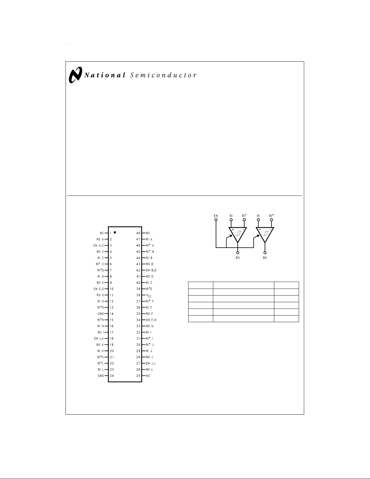
Connection Diagram Function Diagram
48L SSOP
DS89C386
1/6 of package
Truth Table
Enable Inputs Output
EN RI–RI
LXZ
H≥200 mV or OPEN
H ≤ −200 mV L
H +200 mV
†
Not terminated.
>
±
6mA
DS012085-2
*
†
and>−200 mV X
RO
H
DS012085-1
Order Number DS89C386TMEA
See NS Package Number MS48A
TRI-STATE®is a registered trademarkof National Semiconductor Corporation.
© 1998 National Semiconductor Corporation DS012085 www.national.com
Page 2
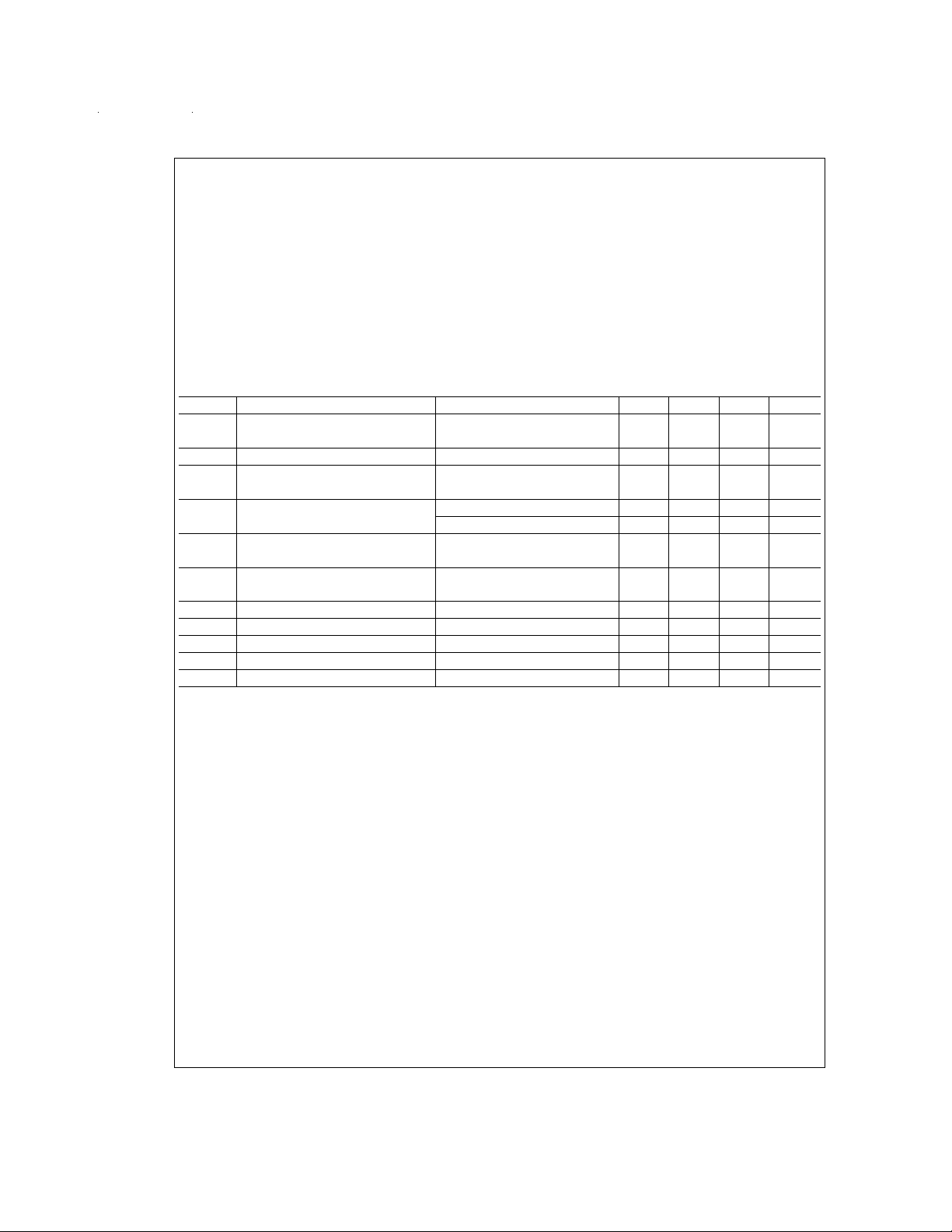
Absolute Maximum Ratings (Notes 1, 2)
If Military/Aerospace specified devices are required,
please contact the National Semiconductor Sales Office/
SSOP Package 1359 mW
±
Current Per Output
25 mA
This device does not meet 2000V ESD rating. (Note 5)
Distributors for availability and specifications.
Supply Voltage (V
Input Common Mode Range (V
Differential Input Voltage (V
Enable Input Voltage (V
Storage Temperature Range (T
) −0.5 to 7V
CC
IN)
)
CM
)
DIFF
) −65˚C to +150˚C
STG
±
14V
±
14V
Lead Temperature (Soldering 4 sec) 260˚C
Operating Conditions
Supply Voltage (V
7V
Operating Temperature Range (T
DS89C386T −40 +85 ˚C
Enable Input Rise or Fall Times 500 ns
) 4.50 5.50 V
CC
)
A
Min Max Unit
Maximum Power Dissipation at 25˚C (Note 4)
DC Electrical Characteristics (Note 3)
=
V
Symbol Parameter Conditions Min Typ Max Units
V
TH
V
HYST
R
IN
I
IN
V
OH
V
OL
V
IH
V
IL
I
OZ
I
I
I
CC
±
10%(unless otherwise specified)
5V
CC
Differential Input Voltage V
Input Hysteresis V
Input Resistance V
=
or V
V
OUT
OH
<
−7V
V
=
0V 70 mV
CM
=
−7V, +7V 5.0 6.8 10 kΩ
IN
OL
<
+7V
CM
−200
±
35 +200 mV
(Other Input=GND)
Input Current V
(Under Test) V
High Level Output Voltage V
Low Level Output Voltage V
Enable High Input Level Voltage 2.0 V
=
+10V, Other Input=GND +1.1 +1.5 mA
IN
=
−10V, Other Input=GND −2.0 −2.5 mA
IN
=
Min., V
CC
=
I
−6.0 mA
OUT
=
Max., V
CC
=
I
6.0 mA
OUT
=
+1V 3.8 4.2 V
(DIFF)
=
−1V 0.2 0.3 V
(DIFF)
CC
V
Enable Low Input Level Voltage GND 0.8 V
TRI-STATE Output Leakage Current V
Enable Input Current V
Quiescent Power Supply Current V
OUT
IN
CC
=
=
V
=
V
CC
Max., V
or GND, EN=V
CC
or GND
=
(DIFF)
IL
+1V 48 69 mA
±
0.5
±
5.0 µA
±
1.0 µA
www.national.com 2
Page 3
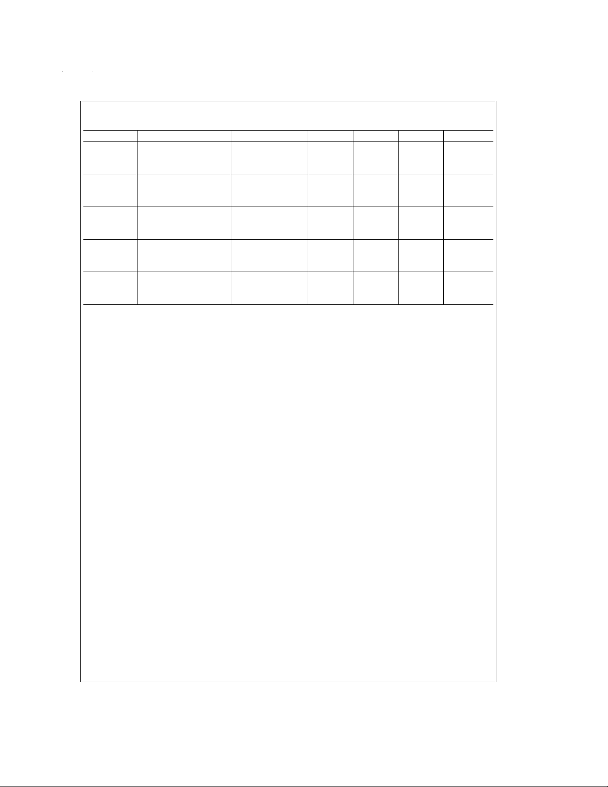
AC Electrical Characteristics (Note 3)
=
V
t
PLH
t
PHL
t
SK
t
RISE
t
FALL
t
PLZ
t
PHZ
t
PZL
t
PZH
Note 1: Absolute Maximum Ratings are those values beyond which the safety of the device cannot be guaranteed. They are not meant to imply that the device
should be operated at these limits. The table of “Electrical Characteristics” provides conditions for actual device operation.
Note 2: Unless otherwise specified, all voltages are referenced to ground.
Note 3: Unless otherwise specified, Min/Max limits apply across the operating temperature range.All typicals are given for V
Note 4: Ratings apply to ambient temperature at 25˚C. Above this temperature derate SSOP (MEA) Package 10.9 mW/˚C.
Note 5: ESD Rating: HEM (1.5 kΩ, 100 pF)
±
10%(
5V
CC
Figures 1, 2, 3
)
Symbol Parameter Conditions Min Typ Max Units
, Propagation Delay C
Input to Output V
Skew C
, Output Rise and C
Fall Times V
, Propagation Delay C
ENABLE to Output R
, Propagation Delay C
ENABLE to Output R
Inputs ≥ 2000V
Outputs ≥ 1000V
EIAJ (0Ω, 200 pF)
All Pins ≥ 350V
=
50 pF
L
=
2.5V 10 19 30 ns
DIFF
=
V
0V
CM
=
50 pF
L
=
V
2.5V 0 2 4 ns
DIFF
=
V
0V
CM
=
50 pF
L
=
2.5V 4 9 ns
DIFF
=
V
0V
CM
=
50 pF
L
=
1000Ω 13 18 ns
L
=
V
2.5V
DIFF
=
50 pF
L
=
1000Ω 13 21 ns
L
=
V
2.5V
DIFF
=
5V and T
CC
=
25˚C.
A
www.national.com3
Page 4

Logic Diagram
Parameter Measurement Information
FIGURE 1. Propagation Delays
www.national.com 4
DS012085-3
DS012085-4
Page 5

Parameter Measurement Information (Continued)
CLIncludes load and test jig capacitance.
for t
, and t
S1=V
CC
S1=GND for t
S1=Open for t
PZL
PZH
PLH,tPHL
, and t
measurements.
PLZ
measurements.
PHZ
, and tSK.
FIGURE 2. Test Circuit for Switching Characteristics
FIGURE 3. TRI-STATE Output Enable and Disable Waveforms
Application Information
*RTis optional although highly recommended to reduce reflections.
FIGURE 4. Two-Wire Balanced System, RS-422
DS012085-5
DS012085-6
DS012085-7
SKEW
Skew may be thought of in a lot of different ways, the next
few paragraphs should clarify what is represented by t
this datasheet and how it is determined. Skew, as used in
SK
this databook, is the absolute value of a mathematical difference between two propagation delays. This is commonlyaccepted throughout the semiconductor industry. However,
there is no standardized method of measuring propagation
delay, from which skew is calculated, of differential line receivers. Elucidating, the voltage level, at which propagation
delays are measured, on both input and output waveforms
are not always consistant. Therefore,skew calculated in this
datasheet, may not be calculated the same as skew defined
in another. This is important to remember whenever making
in
a skew comparison.
Skew may be calculated for the DS89C386, from many dif-
ferent propagation delay measurements. They may be classified into two categories, single-ended and differential.
Single-ended skew is calculated from t
tion delay measurements (see
skew is calculated from t
tion delay measurements (see
PHLD
Figures 5, 6
and t
PLHD
Figures 7, 8
PHL
and t
propaga-
PLH
). Differential
differential propaga-
).
www.national.com5
Page 6

Application Information (Continued)
(Circuit 1)
DS012085-8
FIGURE 5. Circuits for Measuring Single-Ended Propagation Delays (See
Waveforms for Circuit 1
DS012085-10
FIGURE 6. Propagation Delay Waveforms for Circuit 1 and Circuit 2 (See
Figure 6
In
, VX, where X is a number, is the waveform volt-
age level at which the propagation delay measurement either starts or stops. Furthermore, V1 and V2 are normally
identical. The same is true forV3 andV4. However, as mentioned before, these levels are not standardized and may
vary, even with similar devices from other companies. Also
note, V
REF
in
Figure 1
should equal V1 and V2 in
Figure 6
The single-ended skew provides information aboutthe pulse
width distortion of the output waveform. The lower the skew,
the less the output waveform will be distorted. For best case,
skew would be zero, and the output duty cycle would be
50%, assuming the input has a 50%duty cycle.
(Circuit 2)
DS012085-9
Figure 6
)
Waveforms for Circuit 2
DS012085-11
Figure 5
)
Waveforms for Circuit 3
.
(Circuit 3)
DS012085-12
FIGURE 7. Circuit for Measuring Differential
Propagation Delays (See
www.national.com 6
Figure 8
)
DS012085-13
FIGURE 8. Propagation Delay Waveforms
for Circuit 3 (see
Figure 7
)
For differential propagation delays, V1 may not equal V2.
Furthermore, the crossing point of RI and RI
*
corresponds to
zero volts on the differential waveform. (See middle waveform in
Figure 8
.) This is true whether V1 equals V2 or not.
However, if V1 and V2 are specified voltages, then V1 and
V2 are less likely to be equal to the crossing point voltage.
Thus, the differential propagation delays will not be measured from zero volts on the differential waveform.
The differential skew also provides information about the
pulse width distortion of the output waveform relative to the
differential input waveform. The higher the skew, the greater
the distortion of the output waveform.Assuming the differential input has a 50%duty cycle, the output will have a 50
duty cycle if skew equals zero and less than a 50%duty
cycle if skew is greater than zero.
Only t
is specified in this datasheet for the DS89C386. t
SK
is measured singIe-endedly but corresponds to differential
%
SK
Page 7

Application Information (Continued)
skew. Because, for single-ended skew, when V
V1 and V2, t
the crossing point.
PHL
equals t
PHLD
when t
is measured from
PHLD
More information can be calculated from the propagation delays. The channel to channel and device to device skew may
be calculated in addition to the types of skew mentioned previously.These parametersprovide timing performance information beneficial when designing. The channel to channel
skew is calculated from the variation in propagation delay
from receiver to receiver within one package. The device to
device skew is calculated from the variation in propagation
delay from one DS89C386 to another DS89C386.
For the DS89C386, the maximum channel to channel skew
is 20 ns (t
to low propagation delay. The minimum channel to channel
max— tpmin) where tpis the low to high or high
p
skew is 0 ns since it is possible for all 12 receivers to have
identical propagation delays. Note, this is best and worst
case calculations used whenever t
pendently characterized and specified in the datasheet. The
(channel) is not inde-
SK
REF
equals
Typical Performance Characteristics
Receiver Input Voltage vs
Receiver Input Current
(Notes 6, 7)
device to device skew may be calculated in the same way
and the results are identical. Therefore, the device to device
skew is 20 ns and 0 ns maximumand minimum respectively.
TABLE 1. DS89C386 Skew Table
Parameter Min Typ Max Units
t
(diff.) 0 2 4 ns
SK
t
(channel) 0 20 ns
SK
t
(device) 0 20 ns
SK
(diff.) in
Table1
Note t
SK
Also, t
(channel) and tSK(device) are calculations, but are
SK
guaranteed by the propagation delay tests. Both t
nel) and t
specified from characterization data.
(device) would normally be tighter whenever
SK
is the same as tSKin the datasheet.
(chan-
SK
The information in this section of the datasheet is to help
clarify how skew is defined in this datasheet. This should
help when designing the DS89C386 into most applications.
Note 6: The DS89C386 is V.11 compatible. IIN(RI input) is not ≥ 0 when V
conditions.
Note 7: Failsafe (open inputs) is maintained over entire common mode range and operating range
=
3V due to internal failsafe bias resistors (see
IN
DS89C386 Equivalent Input/Output Circuits
FIGURE 9. Receiver Input Equivalent Circuit
DS012085-14
±
10V.
DS012085-15
Figure 6
). See ITU V.11 for complete
www.national.com7
Page 8

DS89C386 Equivalent Input/Output Circuits (Continued)
DS012085-16
FIGURE 10. Receiver Output Equivalent Circuit
FIGURE 11. Receiver Enable Equivalent Circuit
Pin Descriptions
TABLE 2. Device Pin Names and Descriptions
#
Pin
2, 4, 9, 11, 17, 19, 26, RO TTL/CMOS Compatible Receiver Output Pin
28, 33, 35, 41, 43
5, 8, 12, 16, 20, 23, 29, RI Non-Inverting Signal Receiver Input Pin
32, 36, 40, 44, 47
6, 7, 13, 15, 21, 22, 30, RI
31, 37, 39, 45, 46
3, 10, 18, 27, 34, 42 EN Active High Dual Receiver Enabling Pin
38 V
14, 24 GND Device Ground Pin
1, 25, 48 NC Unused Pin (NOT CONNECTED)
www.national.com 8
Pin Name Pin Description
*
CC
DS012085-17
Inverting Signal Receiver Input Pin
Positive Power Supply Pin +5±10
%
Page 9

9
Page 10

Physical Dimensions inches (millimeters) unless otherwise noted
48-Lead (0.300" Wide) Molded Shrink Small Outline Package, JEDEC
Order Number DS89C386TMEA
NS Package Number MS48A
DS89C386 Twelve Channel CMOS Differential Line Receiver
LIFE SUPPORT POLICY
NATIONAL’S PRODUCTS ARE NOT AUTHORIZED FOR USE AS CRITICAL COMPONENTS IN LIFE SUPPORT DEVICES OR SYSTEMS WITHOUT THE EXPRESS WRITTEN APPROVAL OF THE PRESIDENT OF NATIONAL SEMICONDUCTOR CORPORATION. As used herein:
1. Life support devices or systems are devices or systems which, (a) are intended for surgical implant into
the body, or (b) support or sustain life, and whose failure to perform when properly used in accordance
with instructions for use provided in the labeling, can
be reasonably expected to result in a significant injury
to the user.
National Semiconductor
Corporation
Americas
Tel: 1-800-272-9959
Fax: 1-800-737-7018
Email: support@nsc.com
www.national.com
National Semiconductor
Europe
Fax: +49 (0) 1 80-530 85 86
Email: europe.support@nsc.com
Deutsch Tel: +49 (0) 1 80-530 85 85
English Tel: +49 (0) 1 80-532 78 32
Français Tel: +49 (0) 1 80-532 93 58
Italiano Tel: +49 (0) 1 80-534 16 80
2. A critical component in any component of a life support
device or system whose failure to perform can be reasonably expected to cause thefailure ofthe life support
device or system, or to affect its safety or effectiveness.
National Semiconductor
Asia Pacific Customer
Response Group
Tel: 65-2544466
Fax: 65-2504466
Email: sea.support@nsc.com
National Semiconductor
Japan Ltd.
Tel: 81-3-5620-6175
Fax: 81-3-5620-6179
National does not assume any responsibility for use of any circuitry described, no circuit patent licenses are implied and National reserves the right at any time without notice to change said circuitry and specifications.
 Loading...