

Page 1

DS8911/DS8913 AM/FM/TV Sound
Up-Conversion Frequency Synthesizer
General Description
The DS8911 is a digital Phase-Locked Loop (PLL) frequency synthesizer intended for use as a Local Oscillator (LO) in
electronically tuned radios. The device is used in conjunction with a serial data controller, a loop filter, some varactor
diodes and several passive elements to provide the local
oscillator function for both AM and FM tuning.
The conventional superheterodyne AM receiver utilizes a
low IF or down conversion tuning approach whereby the IF
is chosen to be below the frequencies to be received. The
DS8911 PLL on the other hand, utilizes an up-conversion
technique in the AM mode whereby the first IF frequency is
chosen to be well above the RF frequency range to be
tuned. This approach eliminates the need for tuned circuits
in the AM frontend since the image, half IF, and other spurious responses occur far beyond the range of frequencies to
be tuned. Sufficient selectivity and second IF image protection is provided by a crystal filter at the output of the first
mixer.
A significant cost savings can be realized utilizing this upconversion approach to tuning. Removal of the AM tuned
circuits eliminates the cost of expensive matched varactor
diodes and reduces the amount of labor required for alignment down from 6 adjustments to 2. Additional cost savings
are realized because up-conversion enables both the AM
and FM bands to be tuned using a single Voltage Controlled
Oscillator (VCO) operating between 98 and 120 MHz. (The
2 to 1 LO tuning range found in conventional AM down conversion radios is reduced to a 10% tuning range; 9.94 MHz
to 11.02 MHz).
Up-conversion AM tuning is accomplished by first dividing
the VCO signal down by a modulus 10 to obtain the LO
signal. This LO in turn is mixed on chip with the RF signal to
obtain a first IF at the MIXER output pins. This first IF after
crystal filtering is mixed (externally) with a reference frequency provided by the PLL to obtain a 450 kHz second IF
frequency. The DS8911 derives the 450 kHz second IF by
mixing an 11.55 MHz first IF with a 12.00 MHz reference
frequency.
FM and WB (weather band) tuning is done using the conventional down conversion approach. Here the VCO signal
is buffered to produce the LO signal and then mixed on chip
with the RF signal to obtain an IF frequency at the MIXER
output pins. This IF frequency is typically chosen to be 10.7
MHz although placement at 11.50 MHz can further enhance
AM mode performance and minimize IF circuitry.
The PLL provides phase comparator reference frequencies
of 10, 12.5, 25, and 100 kHz. The tuning resolutions resulting from these reference frequencies are determined by dividing the reference by the premix modulus. Table II shows
the tuning resolutions possible.
The DS8911 contains the following logic elements: a voltage controlled oscillator, a reference oscillator, a 14-bit programmable dual-modulus counter, a reference frequency divider chain, a premix divider, a mixer, a phase comparator, a
charge pump, an operational amplifier, and control circuitry
for latched serial data entry.
The DS8913 includes all the above logic elements except
that it requires a 10 MHz reference frequency instead of
12 MHz.
Features
Y
Direct synthesis of LW, MW, SW, FM, and WB
frequencies
Y
Serial data entry for simplified processor control
Y
10, 12.5, 25, and 100 kHz reference frequencies
Y
8 possible tuning resolutions (see Table II)
Y
An op amp with high impedance inputs for loop filtering
Y
Programmable mixer with high dynamic range
DS8911/DS8913 AM/FM/TV Sound Up-Conversion Frequency Synthesizer
April 1990
TRI-STATEÉis a registered trademark of National Semiconductor Corporation.
TM
MICROWIRE
C
1995 National Semiconductor Corporation RRD-B30M105/Printed in U. S. A.
is a trademark of National Semiconductor Corporation.
TL/F/7398
Page 2
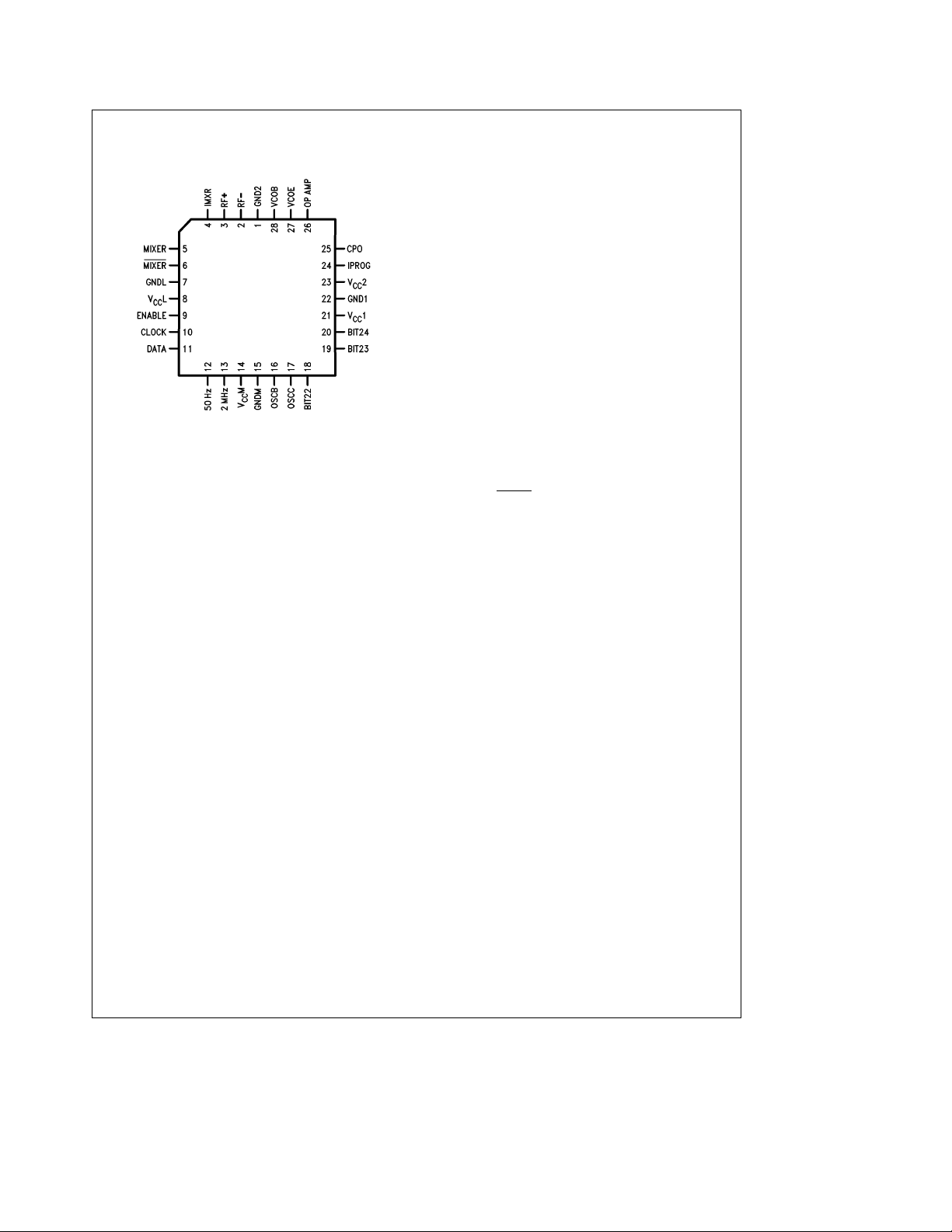
Connection Diagram
Plastic Chip Carrier
Top View
TL/F/7398– 8
Order Number DS8911V/DS8913V
See NS Package Number V28A
Pin Descriptions
V
: The V
CC1
circuitry except the reference divider chain, op amp and mixer sections of the die.
V
: The V
CC2
Op amp.
V
: The V
CCL
for the premix divider and mixer functions.
V
: The V
CCM
reference oscillator and divider chain down through the 50
Hz output, thus enabling low standby current for time-of-day
clock applications.
GND1, GND2, GNDL and GNDM: Provide isolated circuit
ground for the various sections of the device.
DATA and CLOCK: The DATA and CLOCK inputs are for
serial data entry from a controller. They are CMOS inputs
with TTL logic thresholds. The 24-bit data stream is loaded
into the PLL on the positive transition of the CLOCK. The
first 14 bits of the data stream select PLL divide code in
binary form MSB first. The 15th through 24th bits select the
premix modulus, the reference frequency, the bit output
status, and the test/operate modes as shown in Tables I
through V.
ENABLE: The ENABLE input is a CMOS input with a TTL
logic threshold. The ENABLE input enables data when at a
logic ‘‘one’’ and latches data on the transition to a logic
‘‘zero’’.
pin provides a 5V supply source for all
CC1
pin provides a 12V supply source for the
CC2
pin provides an isolated 5V supply source
CCL
pin provides a 5V supply source for the
CCM
BIT Outputs: The open-collector BIT outputs provide either
the status of shift register bits 22, 23, and 24 or enable
access to key internal circuit test nodes. The mode for the
bit outputs is controlled by shift register bits 20 and 21. In
operation, the bit outputs are intended to drive radio functions such as gain, mute, and AM/FM status. These outputs
can also be used to program the loop gain by connection of
an external resistor to IPROG. Bit 24 output can also be
used as a 300 millisecond timer under control of shift register bit 19. During service testing, these pins can be used for
the purpose of either monitoring or driving internal logic
points as indicated in the TEST MODES description under
Table V.
VCOb and VCOe: The Voltage Controlled Oscillator inputs
drive the 14-bit programmable counter and the premix divider. These inputs are the base and emitter leads of a transistor which require connection of a coil, varactor, and several
capacitors to function as a Colpitts oscillator. The VCO is
designed to operate up to 225 MHz. The VCO’s minimum
operating frequency may be limited by the choice of reference frequency and the 961 minimum modulus constraint of
the 31/32 dual modulus counter.
a
RF
and RFb: The Radio Frequency inputs are fed differ-
entially into the mixer.
IMXR: The bias current for the mixer is programmed by connection of an external resistor to this pin. The total mixer
output current equals 4 times the current entering this pin.
MIXER and MIXER
: The MIXER outputs are the collectors
of the double balanced pair mixer transistors. They are intended to operate at voltages greater than V
CC1
.
OSCb and OSCc: The Reference Oscillator inputs are part
of an on-chip Pierce oscillator designed to work in conjunction with 2 capacitors and a crystal resonator. The DS8911
requires a 12 MHz crystal to derive the reference frequencies shown in Table II. The DS8913 requires 10 MHz crystal.
The 12 MHz OSC signal is also used externally as the 2nd
AM LO to obtain a 450 kHz 2nd IF frequency in the AM
mode.
2 MHz: The 2 MHz output is provided to drive a controller’s
clock input.
50 Hz: The 50 Hz output is provided as a time reference for
radios with time-of-day clocks.
IPROG: The IPROG pin enables the charge pump to be
programmed from 0.25 mA to 1.0 mA by connection of an
external resistor to ground.
CPO: The Charge Pump Output circuit sources current if the
VCO frequency is high and sinks current if the VCO frequency is low. The CPO is wired directly to the negative input of
the loop filter op amp.
OP AMP: The OP AMP output is provided for loop filtering.
The op amp has high impedance PMOS gate inputs and is
wired as a transconductance amplifier/filter. The op amp’s
positive input is internally referenced while its negative input
is common with the CPO output.
2
Page 3
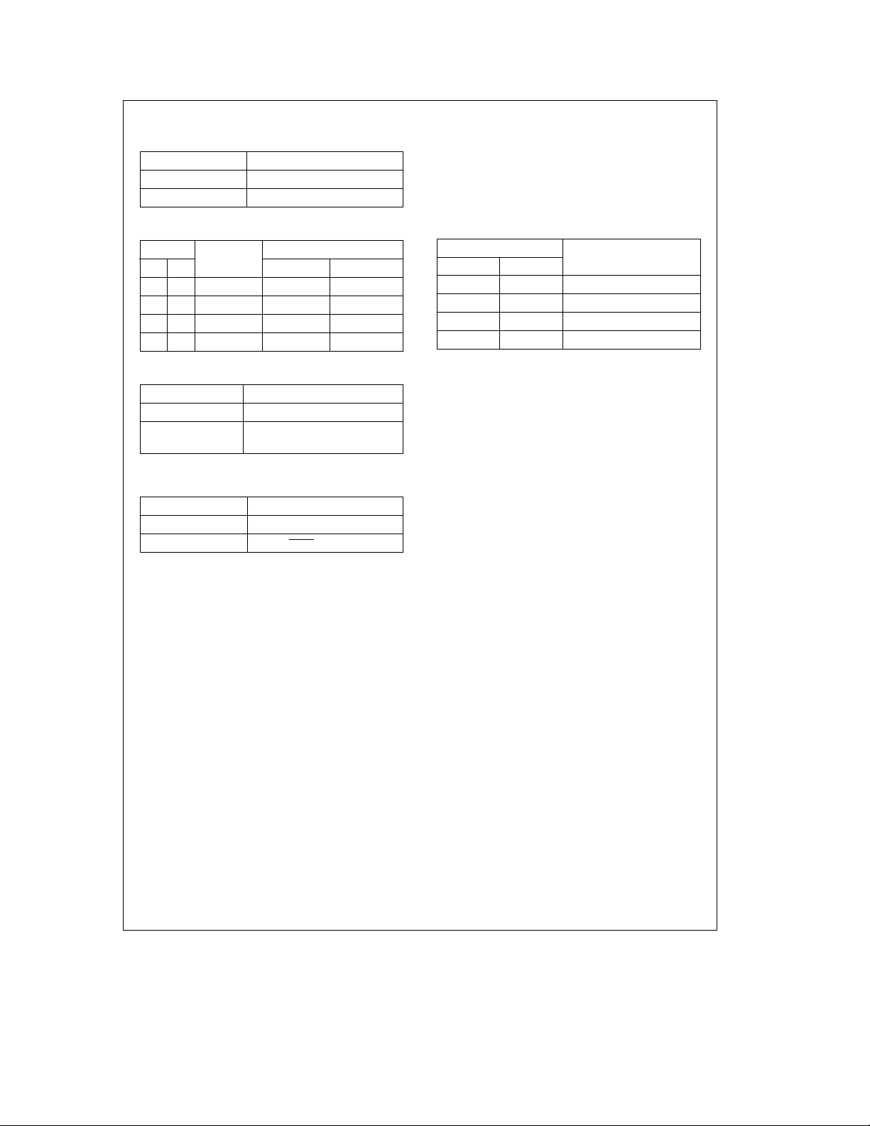
Reference Tables
TABLE I
Bit 15 Premix Modulus
0
1
TABLE II
Bit Reference Tuning Resolution
16 17
Frequency
d
0 0 10 kHz 10 kHz 1 kHz
0 1 12.5 kHz 12.5 kHz 1.25 kHz
1 0 25 kHz 25 kHz 2.5 kHz
1 1 100 kHz 100 kHz 10 kHz
TABLE III
Bit 18 Mode
0 Normal Operation*
1
*The user should always load Bit 18 low.
TABLE IV
Bit 19 Timer
0 Bit 24 Status
1 Bit 24 for 300 ms
TIMER OPERATION
The timer function is provided for use as a retriggerable
‘‘one shot’’ to enable muting for approximately 300 milliseconds after station changes. The timer is enabled at bit 24’s
output if the normal operating mode is selected (shift register bits 20 and 21
e
‘‘LOW’’) and shift register bit 19 data is
latched as a ‘‘HI’’. The timer’s output state will invert immediately upon latching bit 19 ‘‘HI’’ and remain inverted for
approximately 300 milliseconds. If the user readdresses the
device with bit 19 data ‘‘LOW’’ before the timer finishes its
d
1
d
10
1 Premixd10 Premix
Production Test
Mode Only
cycle the timer’s BIT 24 output will finish out the 300 ms
pulse. Readdressing the device with bit 19 ‘‘HI’’ before the
timer finishes its cycle will extend the BIT 24 output pulse
width by 300 ms. Addressing should be performed immediately after the 50 Hz output transitions ‘‘HI’’. BIT 24’s output
state is not guaranteed during the first 300 ms after V
power up as a result of a timer reset in progress.
CC
TABLE V
Bit FUNCTION OF
20 21
PINS 3, 4, & 5
0 0 Status of Bits 22-24
0 1 Test mode 1
1 0 Test mode 2
1 1 Test mode 3
TEST MODE OPERATION
Test Mode 1: Enables the BIT output pins to edge trigger
the phase comparator inputs and monitor an internal lock
detector. BIT 22 negative edge triggers the reference divider input of the phase comparator if the reference divider
state is low. BIT 23 provides the open collector ORing of the
phase comparator’s pump up and down outputs. BIT 24
negative edge triggers the N counter input of the phase
comparator if the N counter state is preconditioned low.
Test Mode 2: Enables the BIT outputs to clock the programmable N counter, monitor its output, and force either its
load or count condition. BIT 22 provides the N counter output which negative edge triggers the phase comparator and
which appears low one N counter clock pulse before it reloads. BIT 23 positive edge triggers the N counter’s clock
input if the prescaler’s output is preconditioned HI. BIT 24
clears the N counter output so that loading will occur on the
next N counter clock edge.
Test Mode 3: Enables the BIT outputs to clock the 50 Hz
and 10 kHz reference dividers and monitor the reference
divider input to the phase comparator. BIT 22 positive edge
clocks the 10 kHz reference divider chain if the 10 kHz output is preconditioned HI. BIT 23 positive edge clocks the 50
Hz divider chain. BIT 24 is the reference divider negative
edge trigger input to the phase comparator.
1
3
Page 4

Absolute Maximum Ratings (Note 1)
If Military/Aerospace specified devices are required,
please contact the National Semiconductor Sales
Office/Distributors for availability and specifications.
Supply Voltage
V
V
V
CCM
CC1
CC2
7V
7V
15V
Input Voltage 7V
Output Voltage
Logic 7V
Op Amp and Mixer Outputs 15V
ESD Sensitivity 1000V
Storage Temperature Range
Lead Temp. (Soldering, 10 seconds) 300§C
Operating Conditions
Min Max Units
V
CCM
V
CC1
V
CC2
Temperature, T
Mixer I
(MixeraMixer Current) 1 20 mA
A
BIAS
3.5 5.5 V
4.5 5.5 V
7.0 12.0 V
b
40
b
65§Ctoa150§C
a
85
C
§
DC Electrical Characteristics (Notes 2 and 3)
Symbol Parameter Test Conditions Min Typ Max Units
V
V
I
I
I
V
V
V
I
I
I
I
I
I
Mixer MixeraMixer V
I
RF
Logic ‘‘1’’ Input Voltage 2.0 V
IH
Logic ‘‘0’’ Input Voltage 0.8 V
IL
Logic ‘‘1’’ Input Current V
IH
Logic ‘‘1’’ Input Current Data, Clock and Enable Inputs, V
I
Logic ‘‘0’’ Input Current Data, Clock and Enable Inputs, V
IL
Logic ‘‘1’’ 2 MHz I
OH
Output Voltage
Op Amp I
Logic ‘‘0’’ 2 MHz I
OL
Output Voltage
50 Hz I
Bit Outputs I
Op Amp I
Op Amp Input VD Op Amp I/O Shorted, V
BIAS
High Level Bit Outputs V
CEX
Output Current
50 Hz V
Mixers V
Charge Pump Program 0.25 mAkI
CPO
Current 2 I
V
CCM
a
CC1
CCL
CC2
BIAS
IN
Note 1: ‘‘Absolute Maximum Ratings’’ are those values beyond which the safety of the device cannot be guaranteed. Except for ‘‘Operating Temperature Range’’,
they are not meant to imply that the device should be operated at these limits.
Note 2: Unless otherwise specified, min/max limits apply across the
Note 3: All currents into device pins are shown as positive, out of device pins as negative, all voltage referenced to ground unless otherwise noted. All values
shown as maximum or minimum on absolute value basis.
Note 4: Total mixer output current (Mixer
Supply Current V
CCM
(Static)
a
V
V
CC1
Supply Current
V
CCL
Supply Current V
CC2
Current (Note 4)
Mixer Input Max Mixer I
Signal Level RF
e
5.5V 10 mA
IN
eb
20 mAV
OH
eb
I
400 mAV
OH
eb
1.0 mA V
OH
e
20 mA 0.3 V
OL
e
I
400 mA 0.4 V
OL
e
250 mA 0.3 V
OL
e
1 mA 0.3 V
OL
e
1.0 mA 1.5 V
OL
e
TRI-STATEÉ, Op Amp IOHvs. IOLApplied
CPO
e
CC1
e
CCM
e
CCL
PROG
Measured I
e
CCM
e
V
5.5V, Bits Hi, I
CC
e
CC2
e
CC1
BIAS
a
or RFbSignal Level
a
Mixer)j4 times the current into the I
e
4.5V, V
3.5V, V
V
CC1
e
8.8V 100 mA
O
e
O
e
4.5V, V
k
1.0 mA Pump-up
CPO
V
CC1/RPROG
to CPO
PROG
5.5V, OSCCeHigh 0.5 1.0 mA
12V 1.5 2.5 mA
e
V
5.5V, MixereMixere12V
CCL
e
20 mA 300 mVrms
b
40§Ctoa85§C temperature range.
e
7V 100 mA
IN
CC1
e
IN
5.5V, V
e
0V
b
0.3 V
CCM
b
2V
CCM
b
1.5 V
CC2
e
12V,
CC2
b
10 mA
200 mV
5.5V 10 mA
e
12V 100 mA
O
,
Pump-down
b
30 2 I
b
30 2 I
PROG
PROG
a
30 %
a
30 %
TRI-STATE 0 100 nA
MXR
and I
Open 25 35 mA
PROG
b
25 4 I
pin.
MXR
MXR
a
25 %
4
Page 5

AC Electrical Characteristics (Note 2)
Symbol Parameter Conditions Min Typ Max Units
t
r
t
f
DATA
DATA
EN
SU
EN
H
EN
PW
CLK
CLK
VCO f
OSC f
SU
H
a
PW
PW
max
max
20%–80% Rise Time 200 ns
80%–20% Fall Time 200 ns
Data Setup Time 100 ns
Data Hold Time
Enable Setup Time 100 ns
V
CC1
e
4.5V to 5.5V
100 ns
Enable Hold Time 100 ns
Enable Positive Pulse Width 200 ns
Clock Positive Pulse Width 200 ns
a
Clock Negative Pulse Width 200 ns
b
VCO Max Frequency See Typical Wiring Diagram 20 225 MHz
Reference Oscillator V
Max Frequency
e
3.5V 12 MHz
CCM
Timing Diagram
MICROWIRETMBus Format
TL/F/7398– 10
TL/F/7398– 19
5
Page 6

TABLE VI. DS8911 Tuning Characteristics
Mode Frequency Range Range
IF Tuning VCO
(MHz) (MHz) (MHz) (kHz) (kHz)
Premix
Modulus
Reference Tuning
Frequency Resolution
Image
(MHz)
LW 11.55/.450 .145 –.290 112.4– 114.1 10 10 1 22–23
MW 11.55/.450 .515 – 1.61 99.4– 110.2 10 10, 12.5, 25, 100 1, 1.25, 2.5, 10 21– 23
SW 11.55/.450 5.94– 6.2 53.5 to 56.1 10 10, 12.5, 25 1, 1.25, 2.5 28 –30
FM 10.7 87.4– 108.1 98.1 –118.8 1 10, 12.5, 25, 100 10, 12.5, 25, 100 109– 130
WB 10.7 162.4 –162.6 151– 152 1 12.5, 25 12.5, 25 140 –142
TV
TV
1
2
10.7 59.75–87.75 70.45– 98.45 1 25 25 81– 109
10.7 179.75–215.75 169.1 –205.1 1 25 25 158 – 194
Input and Output Schematics
TL/F/7398– 11
TL/F/7398– 12
6
Page 7

Input and Output Schematics (Continued)
TL/F/7398– 13
TL/F/7398– 14
TL/F/7398– 15
TL/F/7398– 16
TL/F/7398– 17
TL/F/7398– 18
7
Page 8

Logic Diagram
DS8911/DS8913 PLL Synthesizer
Note 1: The 14 bit programmable N counter is a dual modulus counter with 31/32 prescaler. The minimum continuous modulus of the N counter is
961. (There are a limited number of valid modulus codes below 961.)
*The DS8913 has
d
5
Typical Application Diagram
AM/FM ETR Radio Application
TL/F/7398– 4
TL/F/7398– 5
8
Page 9

Wiring Diagrams
Configuration Using PLL and First Mixer Functions
TL/F/7398– 20
Configuration Using PLL with LO Bypassing Mixer
*The mixer is de-biased by the
100X resistor on the RF
pin to act as an output buffer
for the LO signal.
a
TL/F/7398– 21
9
Page 10

Physical Dimensions inches (millimeters) Lit.
Plastic Chip Carrier (V)
Order Number DS8911V/DS8913V
NS Package Number V28A
Ý
103661
LIFE SUPPORT POLICY
NATIONAL’S PRODUCTS ARE NOT AUTHORIZED FOR USE AS CRITICAL COMPONENTS IN LIFE SUPPORT
DEVICES OR SYSTEMS WITHOUT THE EXPRESS WRITTEN APPROVAL OF THE PRESIDENT OF NATIONAL
SEMICONDUCTOR CORPORATION. As used herein:
DS8911/DS8913 AM/FM/TV Sound Up-Conversion Frequency Synthesizer
1. Life support devices or systems are devices or 2. A critical component is any component of a life
systems which, (a) are intended for surgical implant support device or system whose failure to perform can
into the body, or (b) support or sustain life, and whose be reasonably expected to cause the failure of the life
failure to perform, when properly used in accordance support device or system, or to affect its safety or
with instructions for use provided in the labeling, can effectiveness.
be reasonably expected to result in a significant injury
to the user.
National Semiconductor National Semiconductor National Semiconductor National Semiconductor
Corporation Europe Hong Kong Ltd. Japan Ltd.
1111 West Bardin Road Fax: (
Arlington, TX 76017 Email: cnjwge@tevm2.nsc.com Ocean Centre, 5 Canton Rd. Fax: 81-043-299-2408
Tel: 1(800) 272-9959 Deutsch Tel: (
Fax: 1(800) 737-7018 English Tel: (
National does not assume any responsibility for use of any circuitry described, no circuit patent licenses are implied and National reserves the right at any time without notice to change said circuitry and specifications.
Fran3ais Tel: (
Italiano Tel: (
a
49) 0-180-530 85 86 13th Floor, Straight Block, Tel: 81-043-299-2309
a
49) 0-180-530 85 85 Tsimshatsui, Kowloon
a
49) 0-180-532 78 32 Hong Kong
a
49) 0-180-532 93 58 Tel: (852) 2737-1600
a
49) 0-180-534 16 80 Fax: (852) 2736-9960
 Loading...