

Page 1
0
5
0
www.dalsemi.com
r
www.maxim-ic.com
PRELIMINARY
DS80C400
Network Microcontrolle
GENERAL DESCRIPTION
The DS80C400 is a fast 8051-compatible
microcontroller that executes instructions up to three
times faster than an original 8051 at the same crystal
speed. Its maximum system-clock frequency of
75MHz results in a minimum instruction cycle time
of 54ns. Access to large program or data memory
areas is simplified with a 24-bit addressing scheme
that supports up to 16MB of flat memory. To
accelerate data transfers between the microcontroller
and the 16MB memory map, the DS80C400 provides
four data pointers, each of which can be configured
to automatically increment or decrement upon
execution of certain data pointer-related instructions.
The mircocontroller’s hardware math accelerator
further increases the speed of 32-bit and 16-bit
multiply and divide operations as well as high-speed
shift, normalization, and accumulate functions.
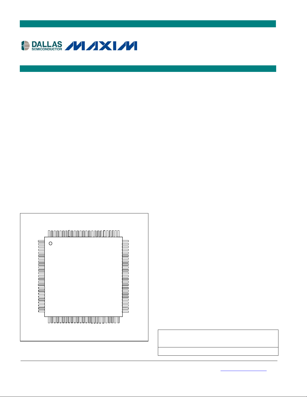
PIN CONFIGURATION
10
1
7
6
7
FEATURES
§ High-Performance Architecture
- Single 8051 instruction cycle in 54ns
- DC to 75MHz clock rate
- Flat 16MB address space
- Four data pointers with auto-increment/
decrement and select-accelerate data movement
- 16/32-bit math accelerator
§ Multitiered Networking and I/O
- 10/100 Ethernet media access controller (MAC)
- CAN 2.0B controller
- 1-Wire
- Three full-duplex hardware serial ports
- Up to eight bidirectional 8-bit ports (64 digital
I/O pins)
§ Robust ROM Firmware
- Supports network boot over Ethernet using
DHCP and TFTP
- Full, application-accessible TCP/IP network
stack
- Supports IPv4 and IPv6
- Implements UDP, TCP, DHCP, ICMP, and
IGMP
- Preemptive, priority-based task scheduler
- MAC address can optionally be acquired from
IEEE-registered DS2502-E48
(Features continued on page 2.)
®
net controller
APPLICATIONS
DS80C400
2
5
2
6
Note: Some revisions of this device may incorporate deviations from published specifications known as errata. Multiple revisions of any device
may be simultaneously available through various sales channels. For information about device errata, click here: www.maxim-ic.com/errata.
LQFP
5
1
5
1 of 125 100902
§ Industrial Control/Automation
§ Vending
§ Data Converters (Serial-to-Ethernet)
§ Data Collection Equipment
§ Environmental Monitoring
§ Home/Office Automation
§ Transaction/Payment Terminals
ORDERING INFORMATION
PART
DS80C400 -40°C to +85°C 75MHz 100 LQFP
TEMP
RANGE
MAX
CLOCK
SPEED
PINPACKAGE
Page 2

FEATURES (continued)
§ 10/100 Ethernet MAC
- Flexible IEEE 802.3 MII (10/100Mbps) and
ENDEC (10Mbps) interfaces allow selection
of PHY
- Low-power operation
- Ultra-low-power sleep mode with Magic
Packet™ and wake-up frame detection
- 8kB on-chip Tx/Rx packet data memory
with buffer control unit reduces load on
CPU
- Half- or full-duplex operation with flow
control
- Multicast/broadcast address filtering with
VLAN support
§ Full-Function CAN 2.0B Controller
- 15 message centers
- Supports standard (11-bit) and extended
(29-bit) identifiers and global masks
- Media byte filtering to support
DeviceNet™, SDS, and higher layer CAN
protocols
- Auto-baud mode and SIESTA low-power
mode
§ Integrated Primary System Logic
- 16 total interrupt sources with 6 external
- Four 16-bit timer/counters
- 2X/4X clock multiplier reduces
electromagnetic interference (EMI)
- Programmable watchdog timer
- Oscillator-fail detection
- Programmable IrDA clock
DS80C400
§ Advanced Power Management
- Energy saving 1.8V Core
- 3.3V I/O operation, 5V tolerant
- Power-management, idle, and stop mode
operations with switchback feature
- Ethernet and CAN shutdown control for
power conservation
- Early warning power-fail interrupt
- Power-fail reset
§ Enhanced Memory Architecture
- Selectable 8/10-bit stack pointer for highlevel language support
- 1kB additional on-chip SRAM usable as
stack/data memory
- 16-bit/24-bit paged/24-bit contiguous
modes
- Selectable multiplexed/nonmultiplexed
external memory interface
- Merged program/data memory space
allows in-system programming
- Defaults to true 8051 memory
compatibility
2 of 125
Page 3
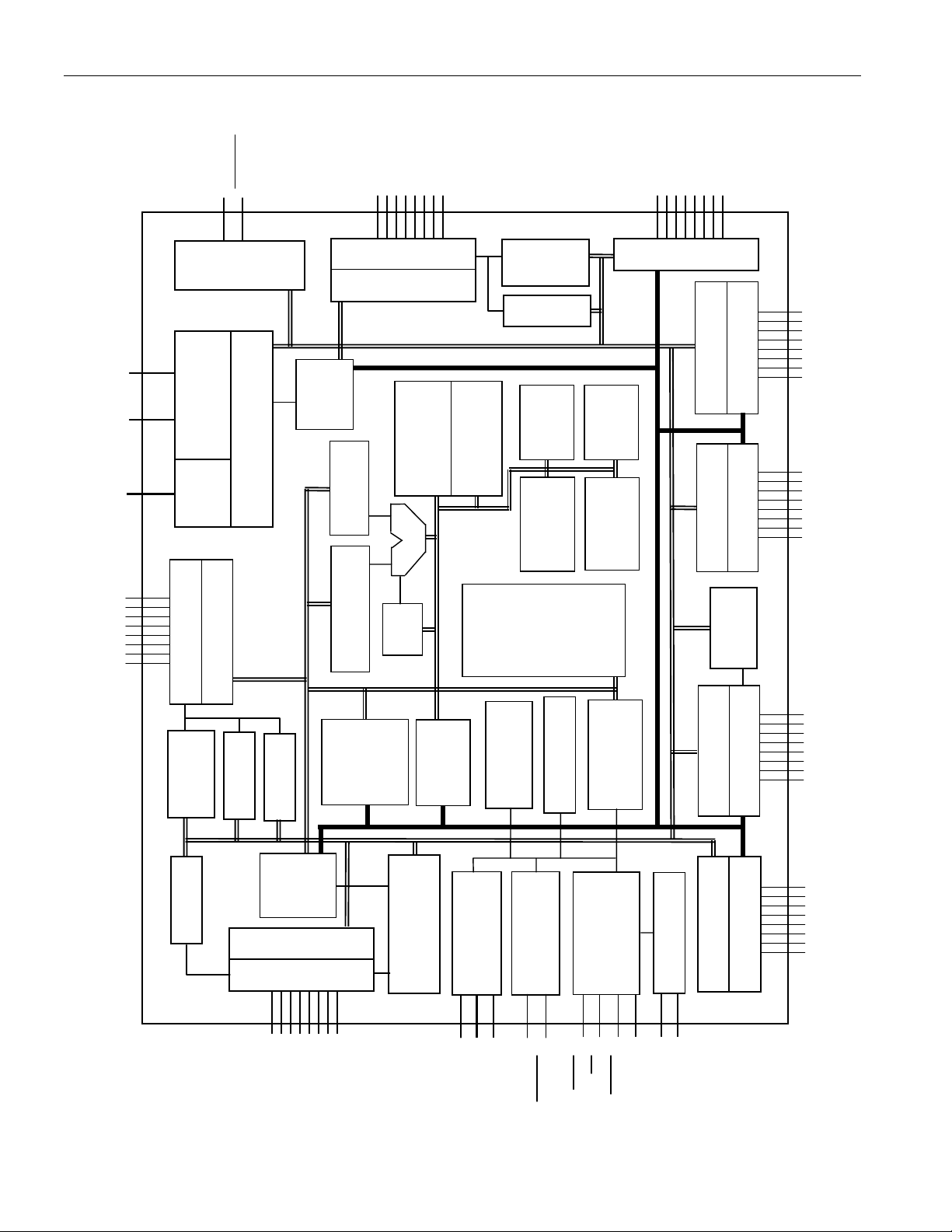
Figure 1. Block Diagram
A
MANAGEMENT
I/O
DS80C400
MDC MDIO
MII I/O (15)
OW
OWSTP
1-WIRE
CONTROLLER
MII
MII
BUFFER CONTROL UNIT
P1.0–P1.7
PORT 1
PORT LATCH
SRAM
9kk x 8
B
P0.0–P0.7
SERIAL
PORT 0
PORT 1
TIMER 2
PORT 7
PORT LATCH
STACK
MATH
ADDER
ONE’S COMP.
ACCELERATOR
POINTER
256 x 8
SFRs/ SRAM
TIMED
INTERRUPT
ACCESS
LOGIC
PORT 2
P2.0–P2.7 P7.0–P7.7
PORT LATCH
P3.0–P3.7
PORT 3
SERIAL
TIMER 3
PORT 0
PORT LATCH
TIMER 0
DATA BUS
TIMER 1
CAN
SRAM
256 x 8
PORT LATCH
PORT 5
P5.0–P5.7
ACCUMULATOR
DPTR0
DPTR1
DPTR2
PSW
DPTR3
CAN 0
CONTROLLER
COUNTER
PROGRAM
POWER
CC
MONITOR
V
(1)
(4)
(4)
SS
CC1
CC3
V
V
V
OSCILLATOR-
FAIL DETECT
ROM
BOOT
64k x 8
WATCHDOG
RESET
CONTROL
RST
RSTOL
REGISTER
INTRUCTION
MEMORY
CONTROL
CLOCK AND
EA
MUX
PSEN
DDRESS BUS
PORT LATCH
PORT LATCH
OSCILLATOR
ALE
XTAL1
XTAL2
SERIAL
PORT 2
PORT 6
PORT 4
P6.0–P6.7
P4.0– 4.7
3 of 125
Page 4

Table 1. Pin Description
PIN NAME FUNCTION
DS80C400
70 V
12, 36,
62, 87
13, 39,
63, 88
68 ALE
CC1
V
CC3
V
SS
+1.8V Core Supply Voltage
+3.3V I/O Supply Voltage
Digital Circuit Ground
Address Latch Enable, Output. When the
MUX pin is low, this pin outputs a clock to
latch the external address LSB from the multiplexed address/data bus on Port 0. This
signal is commonly connected to the latch enable of an external transparent latch. ALE
has a pulse width of 1.5 XTAL1 cycles and a period of four XTAL1 cycles. When the
MUX pin is high, the pin toggles continuously if the ALEOFF bit is cleared. ALE is
forced high when the device is in a reset condition or if the ALEOFF bit is set while the
MUX pin is high.
67
PSEN
Program Store Enable, Output. This signal is the chip enable for external ROM memory.
PSEN provides an active-low pulse and is driven high when external ROM is not being
accessed.
69
40
EA
MUX
External Access Enable, Input. Connect to GND to use external program memory.
Connect to V
to use internal ROM.
CC
Multiplex/Demultiplex Select, Input. This pin selects if the address/data bus operates in
multiplexed (
MUX = 0) or demultiplexed ( MUX = 1) mode. The MUX pin is sampled
only on a power-on reset.
97 RST Reset, Input. The RST input pin contains a Schmitt voltage input to recognize external
active-high reset inputs. The pin also employs an internal pulldown resistor to allow for a
combination of wired-OR external-reset sources. An RC circuit is not required for powerup, as the device provides this function internally.
98
RSTOL
Reset Output Low, Output. This active-low signal is asserted:
when the microcontroller has entered reset through the RST pin; during crystal warm-up
period following power-on or stop mode; during a watchdog timer reset (2 cycles
37,
38
XTAL2,
XTAL1
duration); during an oscillator failure (if OFDE = 1); whenever V
V
RST3
CC1
£ V
XTAL1, XTAL2. Crystal oscillator pins support fundamental mode, parallel resonant, AT
cut crystals. XTAL1 is the input if an external clock source is used in place of a crystal.
RST1
or V
XTAL2 is the output of the crystal amplifier.
AD0–7 (Port 0), I/O. When the MUX pin is connected low, Port 0 is the multiplexed
address/data bus. While ALE is high, the LSB of a memory address is presented. While
ALE falls, the port transitions to a bidirectional data bus. When the
MUX pin is
connected high, Port 0 functions as the bidirectional data bus. Port 0 cannot be modified
by software. The reset condition of Port 0 pins is high. No pullup resistors are needed.
CC3
£
Port Alternate Function
86 AD0/D0 P0.0 AD0/D0 (Address)/Data 0
85 AD1/D1 P0.1 AD1/D1 (Address)/Data 1
84 AD2/D2 P0.2 AD2/D2 (Address)/Data 2
83 AD3/D3 P0.3 AD3/D3 (Address)/Data 3
82 AD4/D4 P0.4 AD4/D4 (Address)/Data 4
81 AD5/D5 P0.5 AD5/D5 (Address)/Data 5
80 AD6/D6 P0.6 AD6/D6 (Address)/Data 6
79 AD7/D7
P0.7 AD7/D7 (Address)/Data 7
4 of 125
Page 5

PIN NAME FUNCTION
P1.0–P1.7 Port 1, I/O. Port 1 can function as either an 8-bit, bidirectional I/O port or as an alternate interface
for internal resources. The reset condition of Port 1 is all bits at logic 1 through a weak pullup. The
logic 1 state also serves as an input mode, since external circuits writing to the port can overdrive
the weak pullup. When software clears any port pin to 0, a strong pulldown is activated that
remains on until either a 1 is written to the port pin or a reset occurs. Writing a 1 after the port has
been at 0 activates a strong transition driver, followed by a weaker sustaining pullup. Once the
momentary strong driver turns off, the port once again becomes the output (and input) high state.
Port Alternate Function
89 P1.0 T2 External I/O for Timer/Counter 2
90 P1.1 T2EX Timer/Counter 2 Capture/Reload Trigger
91 P1.2 RXD1 Serial Port 1 Receive
92 P1.3 TXD1 Serial Port 1 Transmit
93 P1.4 INT2 External Interrupt 2 (Positive Edge Detect)
94
95 P1.6 INT4 External Interrupt 4 (Positive Edge Detect)
96
P1.5
P1.7
A15–A8 (Port 2), Output. Port 2 serves as the MSB for external addressing. The port automatically
asserts the address MSB during external ROM and RAM access. Although the Port 2 SFR exists,
the SFR value never appears on the pins (due to memory access). Therefore, accessing the Port 2
SFR is only useful for MOVX A, @Ri or MOVX @Ri, A instructions, which use the Port 2 SFR
as the external address MSB.
INT3
External Interrupt 3 (Negative Edge Detect)
INT5 External Interrupt 5 (Negative Edge Detect)
DS80C400
Port Alternate Function
66 A8 P2.0 A8 Program/Data Memory Address 8
65 A9 P2.1 A9 Program/Data Memory Address 9
64 A10 P2.2 A10 Program/Data Memory Address 10
61 A11 P2.3 A11 Program/Data Memory Address 11
60 A12 P2.4 A12 Program/Data Memory Address 12
59 A13 P2.5 A13 Program/Data Memory Address 13
58 A14 P2.6 A14 Program/Data Memory Address 14
57 A15 P2.7 A15 Program/Data Memory Address 15
P3.0–P3.7 Port 3, I/O. Port 3 functions as an 8-bit, bidirectional I/O port, and as an alternate interface for
several resources found on the traditional 8051. The reset condition of Port 3 is all bits at logic 1
through a weak pullup. The logic 1 state also serves as an input mode, since external circuits
writing to the port can overdrive the weak pullup. When software clears any port pin to 0, the
device activates a strong pulldown that remains on until either a 1 is written to the port pin or a
reset occurs. Writing a 1 after the port has been at 0 activates a strong transition driver, followed
by a weaker sustaining pullup. Once the momentary strong driver turns off, the port once again
becomes the output (and input) high state.
Port Alternate Function
20 P3.0 RXD0 Serial Port 0 Receive
21 P3.1 TXD0 Serial Port 0 Transmit
22
23
24 P3.4 T0 Timer 0 External Input
25 P3.5 T1/CLKO Timer 1 External Input/External Clock Output
26
27
P3.2
P3.3
P3.6
P3.7
INT0 External Interrupt 0
INT1 External Interrupt 1
WR External Data Memory Write Strobe
RD External Data Memory Read Strobe
5 of 125
Page 6

PIN NAME FUNCTION
P4.0–P4.7 Port 4, I/O. Port 4 can function as an 8-bit, bidirectional I/O port, and as the source for external
address and chip-enable signals for program and data memory. Port pins are configured as I/O or
memory signals through the P4CNT register. The reset condition of Port 4 is all bits at logic 1
through a weak pullup. The logic 1 state also serves as an input mode, since external circuits
writing to the port can overdrive the weak pullup. When software clears any port pin to 0, the
device activates a strong pulldown that remains on until either a 1 is written to the port pin or a
reset occurs. Writing a 1 after the port has been at 0 activates a strong transition driver, followed
by a weaker sustaining pullup. Once the momentary strong driver turns off, the port once again
becomes the output (and input) high state.
Port Alternate Function
48
47
46
45
44 P4.4 A16 Program/Data Memory Address 16
43 P4.5 A17 Program/Data Memory Address 17
42 P4.6 A18 Program/Data Memory Address 18
41 P4.7 A19 Program/Data Memory Address 19
P5.0–P5.7 Port 5, I/O. Port 5 can function as an 8-bit, bidirectional I/O port, the CAN interface, Timer 3
P4.0
P4.1
P4.2
P4.3
input, and/or as peripheral-enable signals. The reset condition of Port 5 is all bits at logic 1 through
a weak pullup. The logic 1 state also serves as an input mode, since external circuits writing to the
port can overdrive the weak pullup. When software clears any port pin to 0, the device activates a
strong pulldown that remains on until either a 1 is written to the port pin or a reset occurs. Writing
a 1 after the port has been at 0 activates a strong transition driver, followed by a weaker sustaining
pullup. Once the momentary strong driver turns off, the port once again becomes the output (and
input) high state.
CE0 Program Memory Chip Enable 0
CE1 Program Memory Chip Enable 1
2CE Program Memory Chip Enable 2
CE3 Program Memory Chip Enable 3
DS80C400
Port Alternate Function
35 P5.0 C0TX CAN0 Transmit Output
34 P5.1 C0RX CAN0 Receive Input
33 P5.2 T3 Timer 3 External Input
32 P5.3 None
31
30
29
28
P5.4
P5.5
P5.6
P5.7
PCE0 Peripheral Chip Enable 0
PCE1 Peripheral Chip Enable 1
PCE2 Peripheral Chip Enable 2
PCE3 Peripheral Chip Enable 3
6 of 125
Page 7

PIN NAME FUNCTION
P6.0–P6.7 Port 6, I/O. Port 6 can function as an 8-bit, bidirectional I/O port, as program and data memory
address/chip-enable signals, and/or a third serial port. The reset condition of Port 6 is all bits at
logic 1 through a weak pullup. The logic 1 state also serves as an input mode, since external
circuits writing to the port can overdrive the weak pullup. When software clears any port pin to 0,
the device activates a strong pulldown that remains on until either a 1 is written to the port pin or a
reset occurs. Writing a 1 after the port has been at 0 activates a strong transition driver, followed
by a weaker sustaining pullup. Once the momentary strong driver turns off, the port once again
becomes the output (and input) high state.
Port Alternate Function
56
55
54
53
52 P6.4 A20 Program/Data Memory Address 20
51 P6.5 A21 Program/Data Memory Address 21
50 P6.6 RXD2 Serial Port 2 Receive
49 P6.7 TXD2 Serial Port 2 Transmit
P6.0
P6.1
P6.2
P6.3
Port 7, I/O. Port 7 can function as either an 8-bit, bidirectional I/O port or the nonmultiplexed A0–
A7 signals (when the
weak pullup. The logic 1 state also serves as an input mode, since external circuits writing to the
port can overdrive the weak pullup. When software clears any port pin to 0, a strong pulldown is
activated that remains on until either a 1 is written to the port pin or a reset occurs. Writing a 1
after the port has been at 0 activates a strong transition driver, followed by a weaker sustaining
pullup. Once the momentary strong driver turns off, the port once again becomes the output (and
input) high state.
CE4 Program Memory Chip Enable 4
CE5 Program Memory Chip Enable 5
CE6 Program Memory Chip Enable 6
CE7 Program Memory Chip Enable 7
MUX pin = 1). The reset condition of Port 7 is all bits at logic 1 through a
DS80C400
Port Alternate Function
78 A0 P7.0 A0 Program/Data Memory Address 0
77 A1 P7.1 A1 Program/Data Memory Address 1
76 A2 P7.2 A2 Program/Data Memory Address 2
75 A3 P7.3 A3 Program/Data Memory Address 3
74 A4 P7.4 A4 Program/Data Memory Address 4
73 A5 P7.5 A5 Program/Data Memory Address 5
72 A6 P7.6 A6 Program/Data Memory Address 6
71 A7 P7.7 A7 Program/Data Memory Address 7
8 TXClk Transmit Clock, Input. The transmit clock is a continuous clock sourced from the Ethernet PHY
controller. It is used to provide timing reference for transferring of TX_EN and TXD[3:0] signals
from the MAC to the external Ethernet PHY controller. The input clock frequency of TXClk
should be 25MHz for 100Mbps operation and 2.5MHz for 10Mbps operation. For ENDEC
operation, TXClk serves the same function, but the input clock frequency should be 10MHz.
7 TX_EN Transmit Enable, Output. The transmit enable is an active-high output and is synchronous with
respect to the TXClk signal. TX_EN is used to indicate valid nibbles of data for transmission on
the MII pins TXD.3–TXD.0. TX_EN is asserted with the first nibble of the preamble and remains
asserted while all nibbles to be transmitted are presented on the TXD.3–TXD.0 pins. TX_EN
negates prior to the first TXClk following the final nibble of the frame. TX_EN serves the same
function for ENDEC operation.
3 TXD.3
4 TXD.2
5 TXD.1
6 TXD.0
Transmit Data, Output. The transmit data outputs provide 4-bit nibbles of data for transmission
over the MII. The transmit data is synchronous with respect to the TXClk signal. For each TXClk
period when TX_EN is asserted,
TXD.3–TXD.0 provides the data for transmission to the Ethernet PHY controller. When TX_EN is
deasserted, the TXD data should be ignored. For ENDEC operation, only TXD.0 is used for
transmission of frames.
7 of 125
Page 8

DS80C400
PIN NAME FUNCTION
10 RXClk Receive Clock, Input. The receive clock is a continuous clock sourced from the Ethernet PHY
controller. It is used to provide timing reference for transferring of RX_DV, RX_ER, and
RXD[3:0] signals from the external Ethernet PHY controller to the MAC. The input clock
frequency of RXClk should be 25MHz for 100Mbps operation and 2.5MHz for 10Mbps operation.
For ENDEC operation, RXClk serves the same function, but the input clock frequency should be
10MHz.
11 RX_DV Receive Data Valid, Input. The receive data valid is an active-high input from the external
Ethernet PHY controller and is synchronous with respect to the RXClk signal. RX_DV is used to
indicate valid nibbles of data for reception on the MII pins RXD.3–RXD.0. RX_DV is asserted
continuously from the first nibble of the frame through the final nibble. RX_DV negates prior to
the first RXClk following the final nibble. RX_DV serves the same function for ENDEC
operation.
9 RX_ER Receive Error, Input. The receive error is an active-high input from the external Ethernet PHY
controller and is synchronous with respect to the RXClk signal. RX_ER is used to indicate to the
MAC that an error (e.g., a coding error, or any error detectable by the PHY) was detected
somewhere in the frame presently being transmitted by the PHY. RX_ER has no effect on the
MAC while RX_DV is deasserted. RX_ER should be low for ENDEC operation.
17 RXD.3
16 RXD.2
15 RXD.1
14 RXD.0
1 CRS Carrier Sense, Input. The carrier sense signal is an active-high input and should be asserted by the
2 COL Collision Detect, Input. The collision detect signal is an active-high input and should be asserted
18 MDC MII Management Clock, Output. The MII management clock is generated by the MAC for use by
19 MDIO MII Management Input/Output, I/O. The MII management I/O is the data pin for serial
99 OW 1-Wire Data, I/O. The 1-Wire data pin is an open-drain, bidirectional data bus for the 1-Wire Bus
100
OWSTP
Receive Data, Input. The receive data inputs provide 4-bit nibbles of data for reception over the
MII. The receive data is synchronous with respect to the RXClk signal. For each RXClk period
when RX_DV is asserted, RXD.3–RXD.0 have the data to be received by the MAC. When
RX_DV is deasserted, the RXD data should be ignored. For ENDEC operation, only RXD.0 is
used for reception of frames.
external Ethernet PHY controller when either the transmit or receive medium is not idle. CRS
should be deasserted by the PHY when the transmit and receive mediums are idle. The PHY
should ensure that the CRS signal remains asserted throughout the duration of a collision
condition. The transitions on the CRS signal need not be synchronous to TXClk or RXClk. CRS
serves the same function for ENDEC operation.
by the external Ethernet PHY controller upon detection of a collision on the medium. The PHY
should ensure that COL remains asserted while the collision condition persists. The transitions on
the COL signal need not be synchronous to TXClk or RXClk. The COL signal is ignored by the
MAC when operating in full-duplex mode. COL serves the same function for ENDEC operation.
the external Ethernet PHY controller as a timing referenced for transferring information on the
MDIO pin. MDC is a periodic signal that has no maximum high or low times. The minimum high
and low times are 160ns each. The minimum period for MDC is 400ns independent of the period
of TXClk and RXClk.
communication with the external Ethernet PHY controller. In a read cycle, data is driven by the
PHY to the MAC synchronously with respect to the MDC clock. In a write cycle, data from the
MAC is output to the external PHY synchronously with respect to the MDC clock.
Master. External 1-Wire slave devices are connected to this pin. This pin must be pulled high by
an external resistor, normally 2.2k.
Strong Pullup Enable, Output. This 1-Wire pin is an open-drain active-low output used to enable
an external strong pullup for the 1-Wire bus. This pin must be pulled high by an external resistor,
normally 10k. This functionality helps recovery times when the 1-Wire bus is operated in
overdrive and long-line standard communication modes. It can optionally be enabled while the bus
master is in the idle state for slave devices requiring sustained high-current operation.
8 of 125
Page 9

DS80C400
DETAILED DESCRIPTION
The DS80C400 is a fast 8051-compatible microcontroller that executes instructions up to three times
faster than an original 8051 at the same crystal speed. Its maximum system-clock frequency of 75MHz
results in a minimum instruction cycle time of 54ns. Access to large program or data memory areas is
simplified with a 24-bit addressing scheme that supports up to 16MB of flat memory. To accelerate data
transfers between the microcontroller and the 16MB memory map, the DS80C400 provides four data
pointers, each of which can be configured to automatically increment or decrement upon execution of
certain data pointer-related instructions. The mircocontroller’s hardware math accelerator further
increases the speed of 32-bit and 16-bit multiply and divide operations as well as high-speed shift,
normalization, and accumulate functions.
With extensive networking and I/O capabilities, the DS80C400 is equipped to serve as a central controller
in a multitiered network. The 10/100 Ethernet media access controller (MAC) enables the DS80C400 to
access and communicate over the Internet. While maintaining a presence on the Internet, the
microcontroller can actively control lower tier networks with dedicated on-chip hardware. These
hardware resources include a full CAN 2.0B controller, a 1-Wire net controller, three full-duplex serial
ports, and eight 8-bit ports (up to 64 digital I/O pins).
Instant connectivity and networking support are provided through an embedded 64kB ROM. This ROM
contains firmware to perform a network boot over an Ethernet connection using DHCP in conjunction
with TFTP. The ROM firmware realizes a full, application-accessible TCP/IP stack, supporting both IPv4
and IPv6, and implements UDP, TCP, DHCP, ICMP, and IGMP. In addition, a priority-based,
preemptive task scheduler is also included. The firmware has been structured so that a MAC address can
optionally be acquired from an IEEE-registered DS2502-E48.
The 10/100 Ethernet MAC featured on the DS80C400 complies with both the IEEE 802.3 MII and
ENDEC PHY interface standards. The MII interface supports 10/100Mbps bus operation, while the
ENDEC interface supports 10Mbps operation. The MAC has been designed for low-power standard
operation and can optionally be placed into an ultra-low-power sleep mode, to be awakened manually or
by detection of a Magic Packet or wake-up frame. Incorporating a buffer control unit reduces the burden
of Ethernet traffic on the CPU. This unit, after initial configuration through an SFR interface, manages all
Tx/Rx packet activity and status reporting through an on-chip 8kB SRAM. To further reduce host
(DS80C400) software intervention, the MAC can be set up to generate a hardware interrupt following
each transmit or receive status report. The DS80C400 MAC can be operated in half-duplex or full-duplex
mode with flow control, and provides multicast/broadcast-address filtering modes as well as VLAN tagrecognition capability.
The DS80C400 features a full-function CAN 2.0B controller. This controller provides 15 total message
centers, 14 of which can be configured as either transmit or receive buffers and one that can serve as a
receive double buffer. The device supports standard 11-bit or 29-extended message identifiers, and offers
two separate 8-bit media masks and media arbitration fields to support the use of higher-level CAN
protocols such as DeviceNet and SDS. A special auto-baud mode allows the CAN controller to quickly
determine required bus timing when inserted into a new network. A SIESTA sleep mode has been made
available for times when the CAN controller can be placed into a power-saving mode.
The DS80C400 has resources that far exceed those normally provided on a standard 8-bit microcontroller.
Many functions, which might exist as peripheral circuits to a microcontroller, have been integrated into
the DS80C400. Some of the integrated functions of the DS80C400 include 16 interrupt sources (six
external), four timer/counters, a programmable watchdog timer, a programmable IrDA output clock, an
oscillator-fail detection circuit, and an internal 2X/4X clock multiplier. This frequency multiplier allows
the microcontroller to operate at full speed with a reduced crystal frequency, reducing EMI.
9 of 125
Page 10

DS80C400
Advanced power-management support positions the DS80C400 for portable and power-conscious
applications. The low-voltage microcontroller core runs from a 1.8V supply while the I/O remains 5V
tolerant, operating from a 3.3V supply. A power-management mode (PMM) allows software to switch
from the standard machine cycle rate of 4 clocks per cycle to 1024 clocks per cycle. For example, 40MHz
standard operation has a machine cycle rate of 10MHz. In PMM, at the same external clock speed,
software can select a 39kHz machine cycle rate, considerably reducing power consumption. The
microcontroller can be configured to automatically switch back from PMM to the faster mode in response
to external interrupts or serial port activity. The DS80C400 provides the ability to place the CPU into an
idle state or an ultra-low-power stop-mode state. As protection against brownout and power-fail
conditions, the microcontroller is capable of issuing an early warning power-fail interrupt and can
generate a power-fail reset.
Defaulting to true 8051-memory compatibility, the microcontroller is most powerful when taking
advantage of its enhanced memory architecture. The DS80C400 has a selectable 10-bit stack pointer that
can address up to 1kB of on-chip SRAM stack space for increased code efficiency. It can be operated in a
24-bit paged or 24-bit contiguous address mode, giving access to a much larger address range than the
standard 16-bit address mode. Support for merged program and data memory access allows in-system
programming, and it can be configured to internally demultiplex data and the lowest address byte, thereby
eliminating the need for an external latch and potentially allowing the use of slower memory devices.
10 of 125
 Loading...