

Datasheet DS80C323-QCD, DS80C323-MCD, DS80C323-ECD, DS80C320-QNL, DS80C320-QNG Datasheet (Dallas Semiconductor)
...Page 1
Note:
Some revisions of this device may incorporate deviations from published specifications known as errata. Multiple
ormation about device errata,
DS80C320/DS80C323
www.m
axim
-
ic.com
FEATURES
§ 80C32-Compatible
- 8051 pin and instruction set compatible
- Four 8-bit I/O ports
- Three 16-bit timer/counters
- 256 bytes scratchpad RAM
- Addresses 64 kB ROM and 64 kB RAM
§ High-speed architecture
- 4 clocks/machine cycle (8032=12)
- DC to 33 MHz (DS80C320)
- DC to 18 MHz (DS80C323)
- Single-cycle instruction in 121 ns
- Uses less power for equivalent work
- Dual data pointer
- Optional variable length MOVX to access
fast/slow RAM/peripherals
§ High integration controller includes:
- Power-fail reset
- Programmable watchdog timer
- Early -warning power-fail interrupt
§ Two full-duplex hardware serial ports
§ 13 total interrupt sources with six external
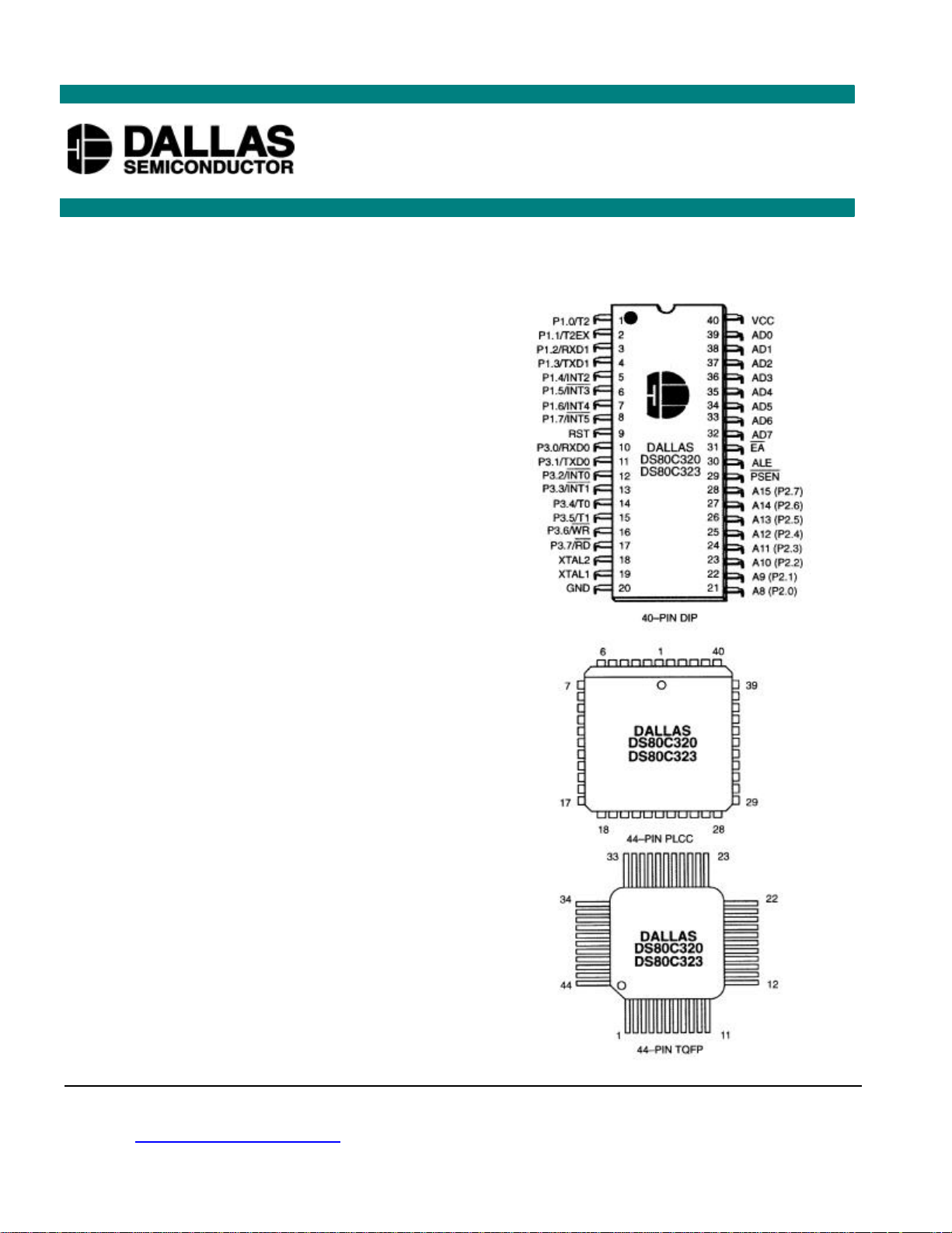
§ Available in 40-pin DIP, 44-pin PLCC and
TQFP
High-Speed/Low-Power Micro
PIN ASSIGNMENT
revisions of any device may be simultaneously available through various sales channels. For inf
click here: http://www.maxim-ic.com/errata.
1 of 42 112299
Page 2
DS80C320/DS80C323
DESCRIPTION
The DS80C320/DS80C323 is a fast 80C31/80C32-compatible microcontroller. Wasted clock and
memory cycles have been removed using a redesigned processor core. As a result, every 8051 instruction
is executed between 1.5 and 3 times faster than the original for the same crystal speed. Typical
applications will see a speed improvement of 2.5 times using the same code and same crystal. The
DS80C320 offers a maximum crystal rate of 33 MHz, resulting in apparent execution speeds of 82.5 MHz
(approximately 2.5X).
The DS80C320/DS80C323 is pin-compatible with all three packages of the standard 80C32 and offers the
same timer/counters, serial port, and I/O ports. In short, the device is extremely familiar to 8051 users but
provides the speed of a 16-bit processor.
The DS80C320 provides several extras in addition to greater speed. These include a second full hardware
serial port, seven additional interrupts, programmable watchdog timer, power-fail interrupt and reset. The
device also provides dual data pointers (DPTRs) to speed block data memory moves. It can also adjust the
speed of off-chip data memory access to between two and nine machine cycles for flexibility in selecting
memory and peripherals.
The DS80C320 operating voltage ranges from 4.25V to 5.5V, making it ideal as a high-performance
upgrade to existing 5V systems. For applications in which power consumption is critical, the DS80C323
offers the same feature set as the DS80C320, but with 2.7V to 5.5V operation.
ORDERING INFORMATION
PART NUMBER PACKAGE MAX CLOCK SPEED TEMPERATURE RANGE
DS80C320-MCG 40-pin plastic DIP 25 MHz 0°C to +70°C
DS80C320-QCG 44-pin PLCC 25 MHz 0°C to +70°C
DS80C320-ECG 44-pin TQFP 25 MHz 0°C to +70°C
DS80C320-MNG 40-pin plastic DIP 25 MHz -40°C to +85°C
DS80C320-QNG 44-pin PLCC 25 MHz -40°C to +85°C
DS80C320-ENG 44-pin TQFP 25 MHz -40°C to +85°C
DS80C320-MCL 40-pin plastic DIP 33 MHz 0°C to +70°C
DS80C320-QCL 44-pin PLCC 33 MHz 0°C to +70°C
DS80C320-ECL 44-pin TQFP 33 MHz 0°C to +70°C
DS80C320-MNL 40-pin plastic DIP 33 MHz -40°C to +85°C
DS80C320-QNL 44-pin PLCC 33 MHz -40°C to +85°C
DS80C320-ENL 44-pin TQFP 33 MHz -40°C to +85°C
DS80C323-MCD 40-pin plastic DIP 18 MHz 0°C to +70°C
DS80C323-QCD 44-pin PLCC 18 MHz 0°C to +70°C
DS80C323-ECD 44-pin TQFP 18 MHz 0°C to +70°C
2 of 42
Page 3
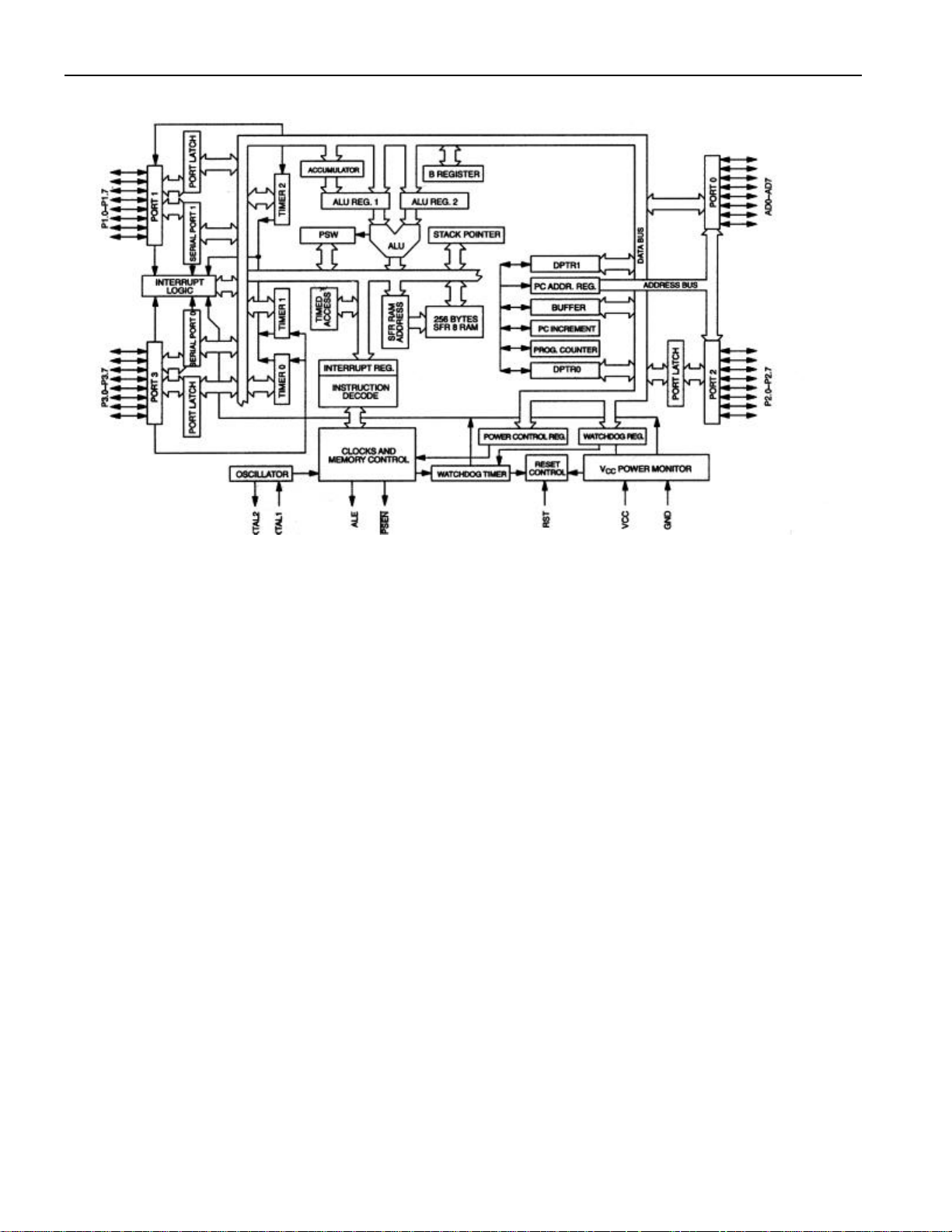
DS80C320 BLOCK DIAGRAM Figure 1
DS80C320/DS80C323
3 of 42
Page 4
DS80C320/DS80C323
commonly connected to external ROM memory as a chip enable.
INT3
INT5
PIN DESCRIPTION Table 1
DIP PLCC TQFP SIGNAL NAME DESCRIPTION
40 44 38 VCC VCC - +5V. (+3V DS80C323)
20 22, 23 16, 17 GND GND - Digital circuit ground.
9 10 4 RST RST - Input. The RST input pin contains a Schmitt voltage input to
recognize external active high Reset inputs. The pin also employs an
internal pulldown resistor to allow for a combination of wired OR
external Reset sources. An RC is not required for power-up, as the
device provides this function internally.
18
19
29 32 26
30 33 27 ALE ALE – Output. The Address Latch Enable output functions as a
39
38
37
36
35
34
33
32
1-8 2-9 40-44
Port Alternate Function
1 2 40 P1.0 T2 External I/O for Timer/Counter 2
2 3 41 P1.1 T2EX Timer/Counter 2 Capture/Reload Trigger
3 4 42 P1.2 RXD1 Serial Port 1 Input
4 5 43 P1.3 TXD1 Serial Port 1 Output
5 6 44 P1.4 INT2 External Interrupt 2 (Positive Edge Detect)
6 7 1
7 8 2 P1.6 INT4 External Interrupt 4 (Positive Edge Detect)
8 9 3
20
21
43
42
41
40
39
38
37
36
14
15
37
36
35
34
33
32
31
30
1-3
XTAL2
XTAL1
XTAL1, XTAL2 - The crystal oscillator pins XTAL1 and XTAL2
provide support for parallel resonant, AT cut crystals. XTAL1 acts
also as an input in the event that an external clock source is used in
place of a crystal. XTAL2 serves as the output of the crystal
amplifier.
PSEN PSEN - Output. The Program Store Enable output. This signal is
PSEN will provide an active low pulse width of 2.25 XTAL1 cycles
with a period of four XTAL1 cycles. PSEN is driven high when data
memory (RAM) is being accessed through the bus and during a reset
condition.
clock to latch the external address LSB from the multiplexed
address/data bus. This signal is commonly connected to the latch
enable of an external 373 family transparent latch. ALE has a pulse
width of 1.5 XTAL1 cycles and a period of four XTAL1 cycles. ALE
is forced high when the device is in a Reset condition.
AD0
AD1
AD2
AD3
AD4
AD5
AD6
AD0-7 (Port 0) - I/O. Port 0 is the multiplexed address/data bus.
During the time when ALE is high, the LSB of a memory address is
presented. When ALE falls, the port transitions to a bi-directional
data bus. This bus is used to read external ROM and read/write
external RAM memory or peripherals. The Port 0 has no true port
latch and can not be written directly by software. The reset condition
of Port 0 is high. No pullup resistors are needed.
AD7
P1.0-P1.7 Port 1 - I/O. Port 1 functions as both an 8-bit bi-directional I/O port
and an alternate functional interface for Timer 2 I/O, new External
Interrupts, and new Serial Port 1. The reset condition of Port 1 is with
all bits at a logic 1. In this state, a weak pullup holds the port high.
This condition also serves as an input mode, since any external
circuit that writes to the port will overcome the weak pullup. When
software writes a 0 to any port pin, the device will activate a strong
pulldown that remains on until either a 1 is written or a reset occurs.
Writing a 1 after the port has been at 0 will cause a strong transition
driver to turn on, followed by a weaker sustaining pullup. Once the
momentary strong driver turns off, the port once again becomes the
output high (and input) state. The alternate modes of Port 1 are
outlined as follows:
P1.5
P1.7
External Interrupt 3 (Negative Edge Detect)
External Interrupt 5 (Negative Edge Detect)
4 of 42
Page 5

DS80C320/DS80C323
INT0
INT1
DIP PLCC TQFP SIGNAL NAME DESCRIPTION
21
22
23
24
25
26
27
28
10-17
Port Alternate Mode
10 11 5 P3.0 RXD0 Serial Port 0 Input
11 13 7 P3.1 TXD0 Serial Port 0 Output
12 14 8
13 15 9
14 16 10 P3.4 T0 Timer 0 External Input
15 17 11 P3.5 T1 Timer 1 External Input
16 18 12
17 19 13
31 35 29
- 12
- 1 39 NC - Reserved. These pins are reserved for additional ground pins
24
25
26
27
28
29
30
31
11,
13-19
34
18
19
20
21
22
23
24
25
5, 7-13 P3.0-P3.7 Port 3 - I/O. Port 3 functions as both an 8-bit bi-directional I/O port
6
28
A8 (P2.0)
A9 (P2.1)
A10 (P2.2)
A11 (P2.3)
A12 (P2.4)
A13 (P2.5)
A14 (P2.6)
A15 (P2.7)
EA EA - Input. This pin must be connected to ground for proper
NC NC - Reserved. These pins should not be connected. They are
A15-A8 (Port 2) - Output . Port 2 serves as the MSB for external
addressing. P2.7 is A15 and P2.0 is A8. The device will
automatically place the MSB of an address on P2 for external ROM
and RAM access. Although Port 2 can be accessed like an ordinary
I/O port, the value stored on the Port 2 latch will never be seen on the
pins (due to memory access). Therefore writing to Port 2 in software
is only useful for the instructions MOVX A, @Ri or MOVX @Ri, A.
These instructions use the Port 2 internal latch to supply the external
address MSB. In this case, the Port 2 latch value will be supplied as
the address information.
and an alternate functional interface for External Interrupts, Serial
Port 0, Timer 0 & 1 Inputs, RD and WR strobes. The reset condition
of Port 3 is with all bits at a logic 1. In this state, a weak pullup holds
the port high. This condition also serves as an input mode, since any
external circuit that writes to the port will overcome the weak pullup.
When software writes a 0 to any port pin, the device will activate a
strong pulldown that remains on until either a 1 is written or a reset
occurs. Writing a 1 after the port has been at 0 will cause a strong
transition driver to turn on, followed by a weaker sustaining pullup.
Once the momentary strong driver turns off, the port once again
becomes both the output high and input state. The alternate modes of
Port 3 are outlined below:
P3.2
P3.3
P3.6 WR External Data Memory Write Strobe
P3.7 RD External Data Memory Read Strobe
operation.
reserved for use with future devices in this family.
on future products.
External Interrupt 0
External Interrupt 1
80C32 COMPATIBILITY
The DS80C320/DS80C323 is a CMOS 80C32-compatible microcontroller designed for high
performance. In most cases it will drop into an existing 80C32 design to significantly improve the
operation. Every effort has been made to keep the device familiar to 8032 users, yet it has many new
features. In general, software written for existing 80C32-based systems will work on the
DS80C320/DS80C323. The exception is critical timing since the High-Speed Microcontroller performs
its instructions much faster than the original. It may be necessary to use memories with faster access
times if the same crystal frequency is used.
Application note 57 “DS80C320 Memory Interface Timing” is a useful tool to help the embedded system
designer select the proper memories for her or his application.
The DS80C320/DS80C323 runs the standard 8051 instruction set and is pin-compatible with an 80C32 in
any of three standard packages. It also provides the same timer/counter resources, full-duplex serial port,
256 bytes of scratchpad RAM and I/O ports as the sta ndard 80C32. Timers will default to a 12 clock per
5 of 42
Page 6
DS80C320/DS80C323
cycle operation to keep timing compatible with original 8051 systems. However, they can be programmed
to run at the new 4 clocks per cycle if desired.
New hardware features are accessed using Special Func tion Registers that do not overlap with standard
80C32 locations. A summary of these SFRs is provided below.
The DS80C320/DS80C323 addresses memory in an identical fashion to the standard 80C32. Electrical
timing will appear different due to the high-speed nature of the product. However, the signals are
essentially the same. Detailed timing diagrams are provided below in the electrical specifications.
This data sheet assumes the user is familiar with the basic features of the standard 80C32. In addition to
these standard features, the DS80C320/DS80C323 includes many new functions. This data sheet provides
only a summary and overview. Detailed descriptions are available in the User’s Guide located in the front
of the High-Speed Microcontroller data book.
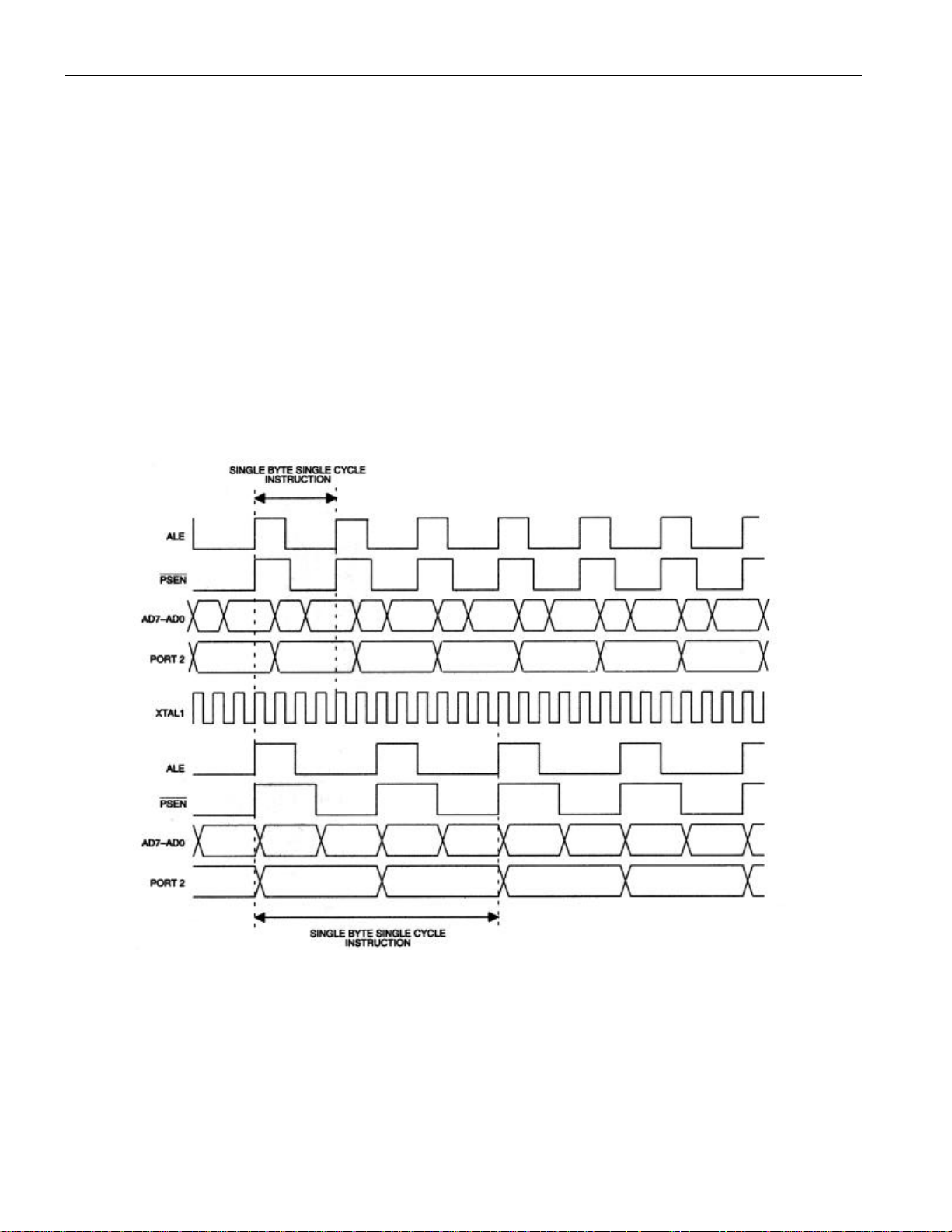
COMPARATIVE TIMING OF THE DS80C320/DS80C323 AND 80C32 Figure 2
DS80C320/DS80C323 TIMING
STANDARD 80C32 TIMING
6 of 42
Page 7

DS80C320/DS80C323
HIGH -SPEED OPERATION
The DS80C320/DS80C323 is built around a high speed 80C32 compatible core. Higher speed comes not
just from increasing the clock frequency, but from a newer, more efficient design.
In this updated core, dummy memory cycles have been eliminated. In a conventional 80C32, machine
cycles are generated by dividing the clock frequency by 12. In the DS80C320/DS80C323, the same
machine cycle is performed in 4 clocks. Thus the fastest instruction, one machine cycle, is executed three
times faster for the same crystal frequency. Note that these are identical instructions. A comparison of the
timing differences is shown in Figure 2. The majority of instructions will see the full 3 to 1 speed
improvement. Some instructions will get between 1.5 and 2.4 X improvement. Note that all instructions
are faster than the original 80C51. Table 2 below shows a summary of the instruction set including the
speed.
The numerical average of all opcodes is approximately a 2.5 to 1 speed improvement. Individual
programs will be affected differently, depending on the actual instructions used. Speed-sensitive
applications would make the most use of instructions that are three times faster. However, the sheer
number of 3 to 1 improved opcodes makes dramatic speed improvements likely for any code. The Dual
Data Pointer feature also allows the user to eliminate wasted instructions when moving blocks of
memory.
INSTRUCTION SET SUMMARY
All instructions in the DS80C320/DS80C323 perform the same functions as their 80C32 counterparts.
Their effect on bits, flags, and other status functions is identical. However, the timing of each instruction
is different. This applies both in absolute and relative number of clocks.
For absolute timing of real-time events, the timing of software loops will need to be calculated using the
table below. However, counter/timers default to run at the older 12 clocks per increment. Therefore, while
software runs at higher speed, timer-based events need no modification to operate as before. Timers can
be set to run at 4 clocks per increment cycle to take advantage of higher speed operation.
The relative time of two instructions might be different in the new architecture than it was previously. For
example, in the original architecture, the “MOVX A, @DPTR” instruction and the “MOV direct, direct”
instruction used two machine cycles or 24 oscillator cycles. Therefore, they required the same amount of
time. In the DS80C320/DS80C323, the MOVX instruction can be done in two machine cycles or eight
oscillator cycles but the “MOV direct, direct” uses three machine cycles or 12 oscillator cycles. While
both are faster than their original counterpa rts, they now have different execution times from each other.
This is because in most cases, the DS80C320/DS80C323 uses one cycle for each byte. The user
concerned with precise program timing should examine the timing of each instruction for familiarity with
the changes. Note that a machine cycle now requires just four clocks, and provides one ALE pulse per
cycle. Many instructions require only one cycle, but some require five. In the original architecture, all
were one or two cycles except for MUL and DIV.
7 of 42
Page 8

DS80C320/DS80C323
INSTRUCTION SET SUMMARY Table 2
Legends:
A - Accumulator
Rn - Register R7 -R0
direct - Internal Register address
@Ri - Internal Register pointed-to by R0 or R1 (except MOVX)
rel - 2’s complement offset byte
bit - direct bit-address
#data - 8-bit constant
#data 16 - 16-bit constant
addr 16 - 16-bit destination address
addr 11 - 11-bit destination address
OSCILLATOR OSCILLATOR
INSTRUCTION BYTE CYCLES INSTRUCTION BYTE CYCLES
Arithmatic Instructions:
ADD A, Rn 1 4 INC A 1 4
ADD A, direct 2 8 INC Rn 1 4
ADD A, @Ri 1 4 INC direct 2 8
ADD A, #data 2 8 INC @Ri 1 4
ADDC A, Rn 1 4 INC DPTR 1 12
ADDC A, direct 2 8 DEC A 1 4
ADDC A, @Ri 1 4 DEC Rn 1 4
ADDC A, #data 2 8 DEC direct 2 8
SUBB A, Rn 1 4 DEC @Ri 1 4
SUBB A, direct 2 8 MUL AB 1 20
SUBB A, @Ri 1 4 DIV AB 1 20
SUBB A, #data 2 8 DA A 1 4
Logical Instructions:
ANL A, Rn 1 4 XRL A, Rn 1 4
ANL A, direct 2 8 XRL A, direct 2 8
ANL A, @Ri 1 4 XRL A, @Ri 1 4
ANL A, #data 2 8 XRL A, #data 2 8
ANL direct, A 2 8 XRL direct, A 2 8
ANL direct, #data 3 12 XRL direct, #data 3 12
ORL A, Rn 1 4 CLR A 1 4
ORL A, direct 2 8 CPL A 1 4
ORL A, @Ri 1 4 RL A 1 4
ORL A, #data 2 8 RLC A 1 4
ORL direct, A 2 8 RR A 1 4
ORL direct, #data 3 12 RRC A 1 4
8 of 42
Page 9

DS80C320/DS80C323
Data Transfer
Instructions:
MOV A, Rn 1 4 MOVC A, @A+DPTR 1 12
MOV A, direct 2 8 MOVC A, @A+PC 1 12
MOV A, @Ri 1 4 MOVX A, @Ri 1 8-36*
MOV A, #data 2 8 MOVX A, @DPTR 1 8-36*
MOV Rn, A 1 4 MOVX @Ri, A 1 8-36*
MOV Rn, direct 2 8 MOVX @DPTR, A 1 8-36*
MOV Rn, #data 2 8 PUSH direct 2 8
MOV direct, A 2 8 POP direct 2 8
MOV direct, Rn 2 8 XCH A, Rn 1 4
MOV direct1, direct2 3 12 XCH A, direct 2 8
MOV direct, @Ri 2 8 XCH A, @Ri 1 4
MOV direct, #data 3 12 XCHD A, @Ri 1 4
MOV @Ri, A 1 4
MOV @Ri, direct 2 8
MOV @Ri, #data 2 8
MOV DPTR, #data 16 3 12
*User Selectable
Bit Manipulation
Instructions:
CLR C 1 4 ANL C, bit 2 8
CLR bit 2 8
SETB C 1 4 ORL C, bit 2 8
SETB bit 2 8
CPL C 1 4 MOV C, bit 2 8
CPL bit 2 8 MOV bit, C 2 8
Program Branching
Instructions:
ACALL addr 11 2 12 CJNE A, direct, rel 3 16
LCALL addr 16 3 16 CJNE A, #data, rel 3 16
RET 1 16 CJNE Rn, #data, rel 3 16
RETI 1 16 CJNE Ri, #data, rel 3 16
AJMP addr 11 2 12 NOP 1 4
LJMP addr 16 3 16 JC rel 2 12
SJMP rel 2 12 JNC rel 2 12
JMP @A+DPTR 1 12 JB bit, rel 3 16
JZ rel 2 12 JNB bit, rel 3 16
JNZ rel 2 12 JBC bit, rel 3 16
DJNZ Rn, rel 2 12
DJNZ direct, rel 3 16
ANL C, bit
ORL C, bit
2 8
2 8
The table above shows the speed for each class of instruction. Note that many of the instructions have
multiple opcodes. There are 255 opcodes for 111 instructions. Of the 255 opcodes, 159 are three times
faster than the original 80C32. While a system that emphasizes those instructions will see the most
improvement, the large total number that receive a 3 to 1 improvement assure a dramatic speed increase
for any system. The speed improvement summary is provided below.
9 of 42
Page 10
DS80C320/DS80C323
SPEED ADVANTAGE SUMMARY
#Opcodes Speed Improvement
159 3.0 x
51 1.5 x
43 2.0 x
2 2.4 x
255 Average: 2.5
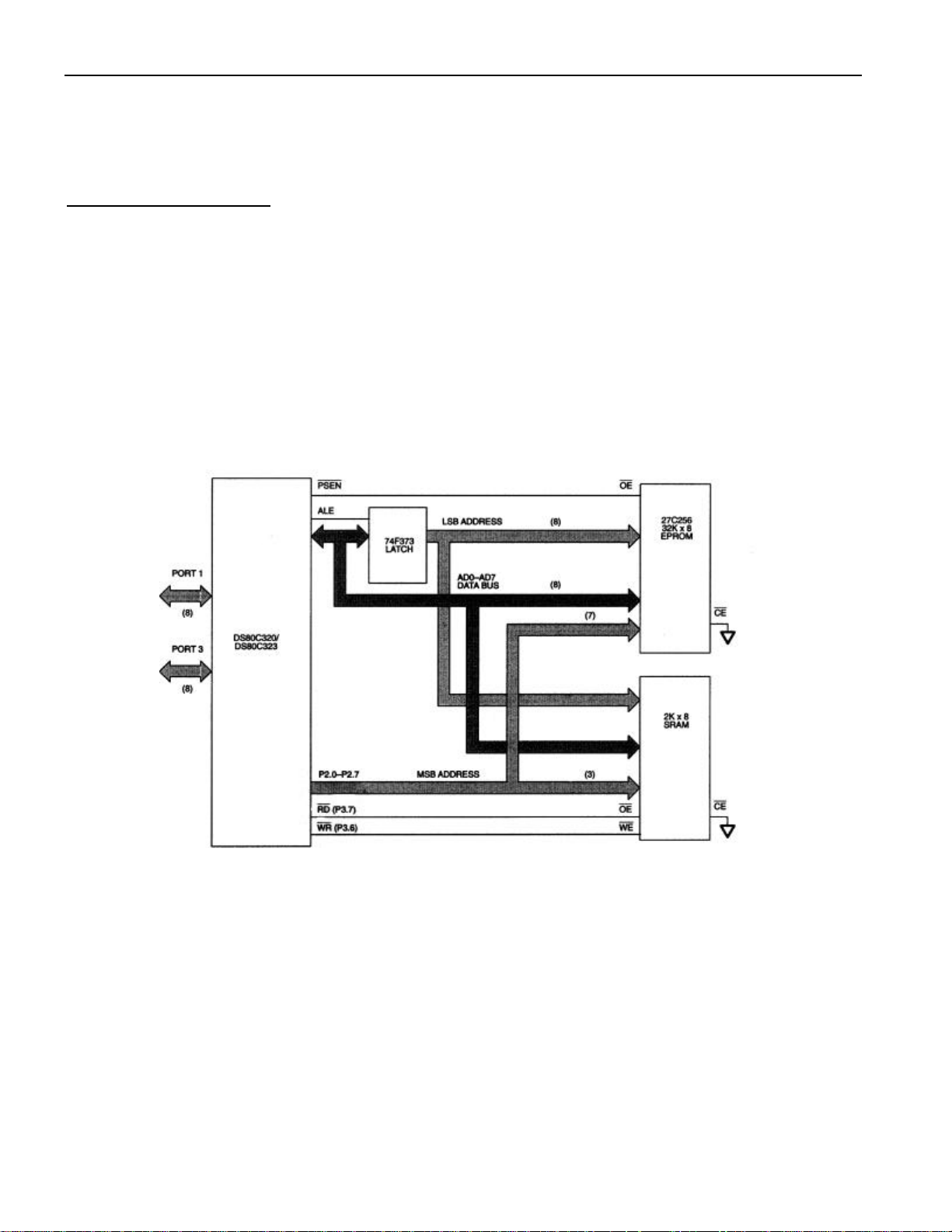
MEMORY ACCESS
The DS80C320/DS80C323 contains no on-chip ROM and 256 bytes of scratchpad RAM. Off-chip
memory is accessed using the multiplexed address/data bus on P0 and the MSB address on P2. A typical
memory connection is shown in Figure 3. Timing diagrams are provided in the Electrical Specifications.
Program memory (ROM) is accessed at a fixed rate determined by the crystal frequency and the actual
instructions. As mentioned above, an instruction cycle requires 4 clocks. Data memory (RAM) is
accessed according to a variable speed MOVX instruction as described below.
TYPICAL MEMORY CONNECTION Figure 3
STRETCH MEMORY CYCLE
The DS80C320/DS80C323 allows the application software to adjust the speed of data memory access.
The microcontroller is capable of performing the MOVX in as little as two instruction cycles. However,
this value can be stretched as needed so that both fast memory and slow memory or peripherals can be
accessed with no glue logic. Even in high-speed systems, it may not be necessary or desirable to perform
data memory access at full speed. In addition, there are a variety of memory mapped peripherals such as
LCD displays or UARTs that are not fast.
The Stretch MOVX is controlled by the Clock Control Register at SFR location 8Eh as described below.
This allows the user to select a stretch value between 0 and 7. A Stretch of 0 will result in a two -machine
cycle MOVX. A Stretch of 7 will result in a MOVX of nine machine cycles. Software can dynamically
change this value depending on the particular memory or peripheral.
10 of 42
Page 11

DS80C320/DS80C323
On reset, the Stretch value will default to a 1, resulting in a three-cycle MOVX. Therefore, RAM access
will not be performed at full speed. This is a convenience to existing designs that may not have fast RAM
in place. When maximum speed is desired, the software should select a Stretch value of 0. When using
very slow RAM or peripherals, a larger stretch value can be selected. Note that this affects data memory
only and the only way to slow program memory (ROM) access is to use a slower crystal.
Using a Stretch value between 1 and 7 causes the microcontroller to stretch the read/write strobe and all
related timing. This results in a wider read/write strobe allowing more time for memory/peripherals to
respond. The timing of the variable speed MOVX is shown in the Electrical Specifications. Note that full
speed access is not the reset default case. Table 3 below shows the resulting strobe widths for each
Stretch value. The memory stretch is implemented using the Clock Control Special Function Register at
SFR location 8Eh. The stretch value is selected using bits CKCON.2-0. In the table, these bits are referred
to as M2 through M0. The first stretch (default) allows the use of common 120 ns or 150 ns RAMs
without dramatically lengthening the memory access.
DATA MEMORY CYCLE STRETCH VALUES Table 3
CKCON.2-0 MEMORY
RD or WR STROBE
MD2 MD1 MD0 CYCLES WIDTH IN CLOCKS TIME @ 25 MHz
0 0 0 2 2 80 ns
0 0 1 3 (default) 4 160 ns
0 1 0 4 8 320 ns
0 1 1 5 12 480 ns
1 0 0 6 16 640 ns
1 0 1 7 20 800 ns
1 1 0 8 24 960 ns
1 1 1 9 28 1120 ns
STROBE WIDTH
11 of 42
Page 12

DS80C320/DS80C323
DUAL DATA POINTER
Data memory block moves can be accelera ted using the Dual Data Pointer (DPTR). The standard 8032
DPTR is a 16-bit value that is used to address off-chip data RAM or peripherals. In the
DS80C320/DS80C323, the standard 16-bit data pointer is called DPTR0 and is located at SFR addresses
82h and 83h. These are the standard locations. The new DPTR is located at SFR 84h and 85h and is
called DPTR1. The DPTR Select bit (DPS) chooses the active pointer and is located at the LSB of the
SFR location 86h. No other bits in register 86h have any effect and are set to 0. The user switches
between data pointers by toggling the LSB of register 86h. The increment (INC) instruction is the fastest
way to accomplish this. All DPTR-related instructions use the currently selected DPTR for any activity.
Therefore only one instruction is required to switch from a source to a destination address. Using the
Dual-Data Pointer saves code from needing to save source and destination addresses when doing a block
move. Once loaded, the software simply switches between DPTR and 1. The relevant register locations
are as follows.
DPL 82h Low byte original DPTR
DPH 83h High byte original DPTR
DPL1 84h Low byte new DPTR
DPH1 85h High byte new DPTR
DPS 86h DPTR Select (LSB)
Sample code listed below illustrates the saving from using the dual DPTR. The example program was
original code written for an 8051 and requires a total of 1869 DS80C320/DS80C323 machine cycles. This
takes 299 µs to execute at 25 MHz. The new code using the Dual DPTR requires only 1097 machine
cycles taking 175.5 µs. The Dual DPTR saves 772 machine cycles or 123.5 µs for a 64-byte block move.
Since each pass through the loop saves 12 machine cycles when compared to the single DPTR approach,
larger blocks gain more efficiency using this feature.
64- BYTE BLOCK MOVE W ITHOUT DUAL DATA POINTER
; SH and SL are high and low byte source address.
; DH and DL are high and low byte of destination address.
# CYCLES
MOV R5, #64d ; NUMBER OF BYTES TO MOVE 2
MOV DPTR, #SHSL ; LOAD SOURCE ADDRESS 3
MOV R1, #SL ; SAVE LOW BYTE OF SOURCE 2
MOV R2, #SH ; SAVE HIGH BYTE OF SOURCE 2
MOV R3, #DL ; SAVE LOW BYTE OF DESTINATION 2
MOV R4, #DH ; SAVE HIGH BYTE OF DESTINATION 2
MOVE:
; THIS LOOP IS PERFORMED THE NUMBER OF TIMES LOADED INTO R5, IN THIS EXAMPLE 64
MOVX A, @DPTR ; READ SOURCE DATA BYTE 2
MOV R1, DPL ; SAVE NEW SOURCE POINTER 2
MOV R2, DPH ; 2
MOV DPL, R3 ; LOAD NEW DESTINATION 2
MOV DPH, R4 ; 2
MOVX @DPTR, A ; WRITE DATA TO DESTINATION 2
INC DPTR ; NEXT DESTINATION ADDRESS 3
MOV R3, DPL ; SAVE NEW DESTINATION POINTER 2
MOV R4, DPH ; 2
MOV DPL, R1 ; GET NEW SOURCE POINTER 2
MOV DPH, R2 ; 2
INC DPTR ; NEXT SOURCE ADDRESS 3
DJNZ R5, MOVE ; FINISHED WITH TABLE? 3
12 of 42
Page 13

DS80C320/DS80C323
64- BYTE BLOCK MOVE WITH DUAL DATA POINTER
; SH and SL are high and low byte source address.
; DH and DL are high and low byte of destination address.
; DPS is the data pointer select. Reset condition is DPS=0, DPTR0 is selected.
# CYCLES
EQU DPS, #86h ; TELL ASSEMBLER ABOUT DPS
MOV R5, #64 ; NUMBER OF BYTES TO MOVE 2
MOV DPTR, #DHDL ; LOAD DESTINATION ADDRESS 3
INC DPS ; CHANGE ACTIVE DPTR 2
MOV DPTR, #SHSL ; LOAD SOURCE ADDRESS 2
MOVE:
; THIS LOOP IS PERFORMED THE NUMBER OF TIMES LOADED INTO R5, IN THIS EXAMPLE 64
MOVX A, @DPTR ; READ SOURCE DATA BYTE 2
INC DPS ; CHANGE DPTR TO DESTINATION 2
MOVX @DPTR, A ; WRITE DATA TO DESTINATION 2
INC DPTR ; NEXT DESTINATION ADDRESS 3
INC DPS ; CHANGE DATA POINTER TO SOURCE 2
INC DPTR ; NEXT SOURCE ADDRESS 3
DJNZ R5, MOVE ; FINISHED WITH TABLE? 3
PERIPHERAL OVERVIEW
Peripherals in the DS80C320/DS80C323 are accessed using Special Function Registers (SFRs). The
device provides several of the most commonly needed peripheral functions in microcomputer-based
systems. These functions are new to the 80C32 family and include a second serial port, Power-fail Reset,
Power-fail Interrupt, and a programmable Watchdog Timer. These are described below, and more details
are available in the High-Speed Microcontroller User’s Guide.
SERIAL PORTS
The DS80C320/DS80C323 provides a serial port (UART) that is identical to the 80C32. Many
applications require serial communication with multiple devices. Therefore a second hardware serial port
is provided that is a full duplicate of the standard one. It optionally uses pins P1.2 (RXD1) and P1.3
(TXD1). This port has duplicate control functions included in new SFR locations. The second serial port
operates in a comparable manner with the first. Both can operate simultaneously but can be at different
baud rates.
The second serial port has similar control registers (SCON1 at C0h, SBUF1 at C1h) to the original. One
difference is that for timer-based baud rates, the original serial port can use Timer 1 or Timer 2 to
generate baud rates. This is selected via SFR bits. The new serial port can only use Timer 1.
TIMER RATE CONTROL
One important difference exists between the DS80C320/DS80C323 and 80C32 regarding timers. The
original 80C32 used a 12 clock per cycle scheme for timers and consequently for some serial baud rates
(depending on the mode). The DS80C320/DS80C323 architecture normally runs using 4 clocks per cycle.
However, in the area of timers, it will default to a 12-clock per cycle scheme on a reset. This allows
existing code with real-time dependencies such as baud rates to operate properly. If an application needs
higher speed timers or serial baud rates, t he timers can be set to run at the 4-clock rate.
The Clock Control register (CKCON - 8Eh) determines these timer speeds. When the relevant CKCON
bit is a logic 1, the device uses 4 clocks per cycle to generate timer speeds. When the control bit is set to a
0, the device uses 12 clocks for timer speeds. The reset condition is a 0. CKCON.5 selects the speed of
13 of 42
Page 14

DS80C320/DS80C323
Timer 2. CKCON.4 selects Timer 1 and CKCON.3 selects Timer 0. Note that unless a user desires very
fast timing, it is unnecessary to alter these bits. Note that the timer controls are independent.
POWER-FAIL RESET
The DS80C320/DS80C323 incorporates a precision band -gap voltage reference to determine when VCC is
out of tolerance. While powering up, internal circuits will hold the device in a reset state until VCC rises
above the V
reset threshold. Once VCC is above this level, the oscillator will begin running. An internal
RST
reset circuit will then count 65536 clocks to allow time for power and the oscillator to stabilize. The
microcontroller will then exit the reset condition. No external components are needed to generate a power
on reset. During power-down or during a severe power glitch, as VCC falls below V
RST
, the
microcontroller will also generate its own reset. It will hold the reset condition as long as power remains
below the threshold. This reset will occur automatically, needing no action from the user or from the
software. Refer to the Electrical Specifications for the exact value of V
RST
.
POWER-FAIL INTERRUPT
The same reference that generates a precision reset threshold can also generate an optional early warning
Power-fail Interrupt (PFI). When enabled by the application software, this interrupt always has the
highest priority. On detecting that the VCC has dropped below V
and that the PFI is enabled, the
PFW
processor will vector to ROM address 0033h. The PFI enable is located in the Watchdog Control SFR
(WDCON - D8h). Setting WDCON.5 to a logic 1 will enable the PFI. The application software can also
read a flag at WDCON.4. This bit is set when a PFI condition has occurred. The flag is independent of
the interrupt enable and software must manually clear it.
WATCHDOG TIMER
For applications that can not afford to run out of control, the DS80C320/DS80C323 incorporates a
programmable watchdog timer circuit. It resets the microcontroller if software fails to reset the watchdog
before the selected time interval has elapsed. The user selects one of four timeout values. After enabling
the watchdog, software must reset the timer prior to expiration of the interval, or the CPU will be reset.
Both the Watchdog Enable and the Watchdog Reset bits are protected by a “Timed Access” circuit. This
prevents accidentally clearing the watchdog. Timeout values are precise since they are related to the
crystal frequency as shown below in Table 4. For reference, the time periods at 25 MHz are also shown.
The watchdog timer also provides a useful option for systems that may not require a reset. If enabled,
then 512 clocks before giving a reset, the watchdog will give an interrupt. The interrupt can also serve as
a convenient time-base generator, or be used to wake-up the processor from Idle mode. The watchdog
function is controlled in the Clock Control (CKCON - 8Eh), Watchdog Control (WDCON - D8h), and
Extended Interrupt Enable (EIE - E8h) SFRs. CKCON.7 and CKCON.6 are called WD1 and WD0
respectively and are used to select the watchdog timeout period as shown in Table 4.
WATCHDOG TIMEOUT VALUES Table 4
INTERRUPT TIME RESET TIME
WD1 WD0 TIMEOUT (@25 MHz) TIMEOUT (@25 MHz)
0 0 217 clocks 5.243 ms 217 + 512 clocks
0 1 220 clocks 41.94 ms 220 + 512 clocks 41.96 ms
5.263 ms j
1 0 223 clocks 335.54 ms 223 + 512 clocks 335.56 ms
1 1 226 clocks 2684.35 ms 226 + 512 clocks 2684.38 ms
14 of 42
Page 15

DS80C320/DS80C323
As shown above, the watchdog timer uses the crystal frequency as a time base. A user selects one of four
counter values to determine the timeout. These clock counter lengths are 2
17
= 131,072 clocks; 2
20
=
1,048,576; 223= 8,388,608 clocks; or 226= 67,108,864 clocks. The times shown in Tab le 4 are with a 25
MHz crystal frequency. Note that once the counter chain has reached a conclusion, the optional interrupt
is generated. Regardless of whether the user enables this interrupt, there are then 512 clocks left until a
reset occurs. There are 5 control bits in special function registers that affect the Watchdog Timer and two
status flags that report to the user. The Reset Watchdog Timer bit (WDCON.0) should be asserted prior to
modifying the Watchdog Timer Mode Select bits (WD1, WD0) to avoid corruption of the watchdog
count.
WDIF (WDCON.3) is the interrupt flag that is set when there are 512 clocks remaining until a reset
occurs. WTRF (WDCON.2) is the flag that is set when a Watchdog reset has occurred. This allows the
application software to determine the source of a reset.
Setting the EWT (WDCON.1) bit enables the Watchdog Timer. The bit is protected by Timed Access
discussed below. Setting the RWT (WDCON.0) bit restarts the Watchdog Timer for another full interval.
Application software must set this bit prior to the timeout. As mentioned previously, WD1 and 0
(CKCON .7 and 6) select the timeout. Finally, the Watchdog Interrupt is enabled using EWDI (EIE.4).
INTERRUPTS
The DS80C320/DS80C323 provides 13 sources of interrupt with three priority levels. The Power-fail
Interrupt (PFI), if enabled, always has the highest priority. There are two remaining user selectable
priorities: high and low. If two interrupts that have the same priority occur simultaneously, the natural
precedence given belo w determines which is a acted upon. Except for the PFI, all interrupts that are new
to the 8051 family have a lower natural priority than the originals.
INTERRUPT PRIORITY Table 5
NAME DESCRIPTION VECTOR NATURAL PRIORITY OLD/NEW
PFI Power-fail Intterupt
INT0
External Interrupt 0 03h 2 OLD
33h j
1 NEW
TF0 Timer 0 0Bh 3 OLD
INT1
External Interrupt 1 13h 4 OLD
TF1 Timer 1 1Bh 5 OLD
SCON0 TI0 or RI0 from serial port 0 23h 6 OLD
TF2 Timer 2 2Bh 7 OLD
SCON1 TI1 or RI1 from serial port 1 3Bh 8 NEW
INT2 External Interrupt 2 43h 9 NEW
INT3
External Interrupt 3 4Bh 10 NEW
INT4 External Interrupt 4 53h 11 NEW
INT5
External Interrupt 5 5Bh 12 NEW
WDTI Watchdog Timeout Interrupt 63h 13 NEW
15 of 42
Page 16

DS80C320/DS80C323
POWER MANAGEMENT
The DS80C320/DS80C323 provides the standard Idle and power-down (Stop) that are available on the
standard 80C32. However the device has enhancements that make these modes more useful, and allow
more power saving.
The Idle mode is invoked by setting the LSB of the Power Control register (PCON - 87h). Idle will leave
internal clocks, serial port and timer running. No memory access will be performed so power is
dramatically reduced. Since clocks are running, the Idle power consumption is related to crystal
frequency. It should be approximately ½ of the operational power. The CPU can exit the Idle state with
any interrupt or a reset.
The power-down or Stop mode is invoked by setting the PCON.1 bit. Stop mode is a lower power state
than Idle since it turns off all internal clocking. The ICC of a standard Stop mode is approximately 1 µA
but is specified in the Electrical Specifications. The CPU will exit Stop mode from an external interrupt
or a reset condition.
Note that internally ge nerated interrupts (timer, serial port, watchdog) are not useful in Idle or Stop since
they require clocking activity.
IDLE MODE ENHANCEMENTS
A simple enhancement to Idle mode makes it substantially more useful. The innovation involves not the
Idle mode itself, but the watchdog timer. As mentioned above, the Watchdog Timer provides an optional
interrupt capability. This interrupt can provide a periodic interval timer to bring the
DS80C320/DS80C323 out of Idle mode. This can be useful even if the Watchdog is not normally used.
By enabling the Watchdog Timer and its interrupt prior to invoking Idle, a user can periodically come out
of Idle perform an operation, then return to Idle until the next operation. This will lower the overall power
consumption. When using the Watchdog Interrupt to cancel the Idle state, make sure to restart the
Watchdog Timer or it will cause a reset.
STOP MODE ENHANCEMENTS
The DS80C320/DS80C323 provides two enhancements to the Stop mode. As documented above, the
device provides a band-gap reference to determine Power-fail Interrupt and Reset thresholds. The default
state is that the band-gap reference is off when Stop mode is invoked. This allows the extremely low
power state mentioned above. A user can optionally choose to have the band-gap enabled during Stop
mode. This means that PFI and power-fail reset will be activated and are valid means for leaving Stop
mode.
In Stop mode with the band -gap on, ICC will be approximately 50 µA compared with 1 µA with the band gap off. If a user does not require a Power-fail Reset or Interrupt while in Stop mode, the band -gap can
remain turned off. Note that only the most power sensitive applications should turn off the band -gap, as
this results in an uncontrolled power down condition.
The control of the band-gap reference is located in the Extended Interrupt Flag register (EXIF - 91h).
Setting BGS (EXIF.0) to a 1 will leave the band -gap reference enabled during Stop mode. The default or
reset condition is with the bit at a logic 0. This results in the band-gap being turned off during Stop mode.
Note that this bit has no control of the reference during full power or Idle modes.
16 of 42
Page 17

DS80C320/DS80C323
The second feature allows an additional power saving option. This is the ability to start instantly when
exiting Stop mo de. It is accomplished using an internal ring oscillator that can be used when exiting Stop
mode in response to an interrupt. The benefit of the ring oscillator is as follows.
Using Stop mode turns off the crystal oscillator and all internal clocks to save power. This requires that
the oscillator be restarted when exiting Stop mode. Actual start-up time is crystal dependent, but is
normally at least 4 ms. A common recommendation is 10 ms. In an application that will wake-up,
perform a short operation, then return to sleep, the crystal start-up can be longer than the real transaction.
However, the ring oscillator will start instantly. The user can perform a simple operation and return to
sleep before the crystal has even stabilized. If the ring is used to start and the processor remains running,
hardware will automatically switch to the crystal once a power-on reset interval (65536 clocks) has
expired. This value is used to guarantee stability even though power is not being cycled.
If the user returns to Stop mode prior to switching of crystal, then all clocks will be turned off again. The
ring oscillator runs at approximately 3 MHz (1.5 MHz at 3V) but will not be a precision value. No realtime precision operations (including serial communication) should be conducted during this ring period.
Figure 7 shows how the operation would compare when using the ring, and when starting up normally.
The default state is to come out of Stop mode without using the ring oscillator.
This function is controlled using the RGSL - Ring Select bit at EXIF.1 (EXIF - 91h). When EXIF.1 is set,
the ring oscillator will be used to come out of Stop mode quickly. As mentioned above, the processor will
automatically switch from the ring (if enabled) to the crystal after a delay of 65536 crystal clocks. For a
3.57 MHz crystal, this is approximately 18 ms. The processor sets a flag called RGMD - Ring Mode to
tell software that the ring is being used. This bit at EXIF.2 will be a logic 1 when the ring is in use. No
serial communication or precision timing should be attempted while this bit is set, since the operating
frequency is not precise.
RING OSCILLATOR START-UP Figure 4
Diagram assumes that the operation following Stop requires less than 18 ms complete.
17 of 42
Page 18

DS80C320/DS80C323
TIMED ACCESS PROTECTION
Selected SFR bits are critical to operation, making it desirable to protect against an accidental write
operation. The Timed Access procedure prevents an errant CPU from accidentally altering a bit that
would cause difficulty. The Timed Access procedure requires that the write of a protected bit be
preceded by the following instructions:
MOV 0C7h, #0AAh
MOV 0C7h, #55h
By writing an AAh followed by a 55h to the Timed Access register (location C7h), the hardware opens a
three-cycle window that allows software to modify one of the protected bits. If the instruction that seeks
to modify the protected bit is not immediately proceeded by these instructions, the write will not take
effect. The protected bits are:
EXIF.0 BGS Band -gap Select
WDCON.6 POR Power-on Re set flag
WDCON.1 EWT Enable Watchdog
WDCON.0 RWT Reset Watchdog
WDCON.3 WDIF Watchdog Interrupt Flag
SPECIAL FUNCTION REGISTERS
Most special features of the DS80C320/DS80C323 or 80C32 are controlled by bits in special function
registers (SFRs). This allows the device to add many features but use the same instruction set. When
writing software to use a new feature, the SFR must be defined to an assembler or compiler using an
equate statement. This is the only change needed to access the new function. The DS80C320/DS80C323
duplicates the SFRs that are contained in the standard 80C32. Table 6 shows the register addresses and bit
locations. Many are standard 80C32 registers. The High-Speed Microcontroller User’s Guide describes
all SFRs.
18 of 42
Page 19

DS80C320/DS80C323
SPECIAL FUNCTION REGI STER LOCATIONS Table 6
REGISTER BIT 7 BIT 6 BIT 5 BIT 4 BIT 3 BIT 2 BIT 1 BIT 0 ADDRESS
SP 81h
DPL 82h
DPH 83h
DPL1 84h
DPH1 85h
DPS 0 0 0 0 0 0 0 SEL 86h
PCON SMOD_0 SMOD0 - - GF1 GF0 STOP IDLE 87h
TCON TF1 TR1 TF0 TR0 IE1 IT1 IE0 IT0 88h
TMOD GATE
TL0 8Ah
TL1 8Bh
TH0 8Ch
TH1 8Dh
CKCON WD1 WD0 T2M T1M T0M MD2 MD1 MD0 8Eh
P1 P1.7 P1.6 P1.5 P1.4 P1.3 P1.2 P1.1 P1.0 90h
EXIF IE5 IE4 IE3 IE2 - RGMD RGSL BGS 91h
SCON0 SM0/FE_0 SM1_0 SM2_0 REN_0 TB8_0 RB8_0 TI_0 RI_0 98h
SBUF0 99h
P2 P2.0 P2.6 P2.5 P2.4 P2.3 P2.2 P2.1 P2.0 A0h
IE EA ES1 ET2 ES0 ET1 EX1 ET0 EX0 A8h
SADDR0 A9h
SADDR1 AAh
P3 P3.7 P3.6 P3.5 P3.4 P3.3 P3.2 P3.1 P3.0 B0h
IP - PS1 PT2 PS0 PT1 PX1 PT0 PX0 B8h
SADEN0 B9h
SADEN1 BAh
SCON1 SM0/FE_0 SM1_0 SM2_0 REN_0 TB8_0 RB8_0 TI_0 RI_0 C0h
SBUF1 C1h
STATUS PIP HIP LIP 1 1 1 1 1 C5h
TA C7h
T2CON TF2 EXF2 RCLK TCLK EXEN2 TR2
T2MOD - - - - - - T2OE DCEN C9h
RCAP2L CAh
RCAP2H CBh
TL2 CCh
TH2 CDh
PSW CY AC F0 RS1 RS0 OV FL P D0h
WDCON SMOD_1 POR EPFI PFI WDIF WTRF EWT RWT D8h
ACC E0h
EIE - - - EWDI EX5 EX4 EX3 EX2 E8h
B F0h
EIP - - - PWDI PX5 PX4 PX3 PX2 F8h
C/ T
M1 M0 GATE
C/ T
M1 M0 89h
C/ T2 CP/ RL2
C8h
19 of 42
Page 20

DS80C320/DS80C323
ELECTRICAL SPECIFICATIONS
ABSOLUTE MAXIMUM RATINGS*
Voltage on Any Pin Relative to Ground -0.3V to (VCC + 0.5V)
Voltage on VCC Relative to Ground -0.3V to +6.0V
Operating Temperature -40°C to +85°C
Storage Temperature -55°C to +125°C
Soldering Temperature 160°C for 10 seconds
* This is a stress rating only and functional operation of the device at these or any other conditions
above those indicated in the operation sections of this specification is not implied. Exposure to
absolute maximum rating conditions for extended periods of time may affect reliability.
DS80C320 DC ELECTRICAL CHARACTERISTICS
PARAMETER SYMBOL MIN TYP MAX UNITS NOTES
Operating Supply Voltage VCC 4.5 5.0 5.5 V 1
Power-fail Warning V
Minimum Operating Voltage V
Supply Current Active Mode
@ 25 MHz
Supply Current Idle Mode
@ 25 MHz
Supply Current Active Mode
@ 33 MHz
Supply Current Idle Mode
@ 33 MHz
Supply Current Stop Mode,
Band-gap Reference Disabled
Supply Current Stop Mode,
Band-gap Reference Enabled
Input Low Level VIL -0.3 +0.8 V 1
Input High Level
(Except XTAL1 and RST)
Input High Level XTAL1 and RST V
Output Low Voltage Ports 1, 3,
@ IOL = 1.6 mA
Output Low Voltage Ports 0, 2,
ALE, PSEN @ IOL = 3.2 mA
Output High Voltage Ports 1, 3,
ALE, PSEN @ IOH = -50 µA
Output High Voltage Ports 1, 3,
@ I
= -1.5 mA
OH
Output High Voltage Ports 0, 2,
ALE, PSEN @ IOH = -8 mA
Input Low Current Ports 1, 3
@ 0.45V
Transition Current from 1 to 0
Ports 1, 3 @ 2V
Input Leakage Port 0, Bus Mode IL -300 +300 µA 9
RST Pulldown Resistance R
4.25 4.38 4.55 V 1
PFW
4.0 4.1 4.25 V 1, 12
RST
ICC 30 45 mA 2
I
15 25 mA 3
IDLE
ICC 35 mA 2
I
20 mA 3
IDLE
I
.01 1 µA 4
STOP
I
50 80 µA 4, 10
SPBG
V
2.0 VCC+0.3 V 1
IH1
3.5 VCC+0.3 V 1
IH2
V
0.45 V 1
OL1
V
0.45 V 1, 5
OL2
V
2.4 V 1, 6
OH1
V
2.4 V 1, 7
OH2
V
2.4 V 1, 5
OH3
IIL -55 µA 11
ITL -650 µA 8
50 170 kO
RST
20 of 42
Page 21

DS80C320/DS80C323
NOTES FOR DS80C320 DC ELECTRICAL CHARACTERISTICS:
All parameters apply to both commercial and industrial temperature operation unless otherwise noted.
1. All voltages are referenced to ground.
2. Active current is measured with a 25 MHz clock source driving XTAL1, VCC=RST=5.5V, all other
pins disconnected.
3. Idle mode current is measured with a 25 MHz clock source driving XTAL1, VCC=5.5V, RST at
ground, all other pins disconnected.
4. Stop mode current measured with XTAL1 and RST grounded, VCC=5.5V, all other pins disconnected.
when addressing external memory.
5. When addressing external memory.
6. RST=VCC. This condition mimics operation of pins in I/O mode.
7. During a 0 to 1 transition, a one-shot drives the ports hard for two clock cycles. This measurement
reflects port in transition mode.
8. Ports 1, 2, and 3 source transition current when being pulled down externally. It reaches its maximum
at approximately 2V.
9. 0.45<VIN<VCC. Not a high impedance input. This port is a weak address holding latch because Port 0
is dedicated as an address bus on the DS80C320. Peak current occurs near the input transition point of
the latch, approximately 2V.
10. Over the industrial temperature range, this specification has a maximum value of 200 µA.
11. This is the current required from an external circuit to hold a logic low level on an I/O pin while the
corresponding port latch bit is set to 1. This is only the current required to hold the low level;
transitions from 1 to 0 on an I/O pin will also have to overcome the transition current.
12. Device operating range is 4.5V to 5.5V; however, device is tested to 4.0V to ensure proper operation
at minimum V
RST
.
21 of 42
Page 22

TYPICAL ICC VERSUS FREQUENCY Figure 5
DS80C320 AC CHARACTERISTICS UP TO 25 MHz
PARAMETER SYMBOL 25
MHz
MIN
Oscillator Freq.
1/t
CLCL
(Ext. Osc.)
(Ext. Crystal)
ALE Pulse Width t
Port 0 Address Valid
50 1.5t
LHLL
t
9 0.5t
AVLL
to ALE Low
Address Hold After
t
5 note 5 0.25t
LLAX1
ALE Low
Address Hold After
t
13 0.5t
LLAX2
ALE Low for MOVX
WR
ALE Low to Valid
t
73 2.5t
LLIV
Instruction In
t
3 0.25t
ALE Low to PSEN Low
PSEN Pulse Width
PSEN Low to Valid
LLPL
t
83 2.25t
PLPH
t
69 2.25t
PLIV
Instruction In
Input Instruction Hold
t
0 0 ns
PXIX
After PSEN
Input Instruction Float
t
35 t
PXIZ
After PSEN
Port 0 Address to Valid
t
93 3t
AVIV1
Instruction In
Port 2 Address to Valid
t
107 3.5t
AVIV2
Instruction In
t
note 5 note 5 ns
PSEN Low to
PLAZ
Address Float
0
1
22 of 42
25
MHz
MAX
25
25
VARIABLE
CLOCK
MIN
0
1
-10 ns
CLCL
-11 ns
CLCL
CLCL
-7 ns
CLCL
CLCL
CLCL
DS80C320/DS80C323
VARIABLE
UNITS
CLOCK
MAX
25
25
MHz
-5 note 5 ns
-27 ns
CLCL
-7 ns
-7 ns
-21 ns
CLCL
-5 ns
CLCL
-27 ns
CLCL
-33 ns
CLCL
Page 23

DS80C320/DS80C323
NOTES FOR AC ELECTRICAL CHARACTERISTICS:
All parameters apply to both commercial and industrial temperature range operation unless otherwise
noted. AC timing characteristics valid for oscillator frequency > 16 MHz.
1. All signals rated over operating temperature at 25 MHz.
2. All signals characterized with load capacitance of 80 pF except Port 0, ALE, PSEN , RD and WR at
100 pF. Note that loading should be approximately equal for valid timing.
3. Interfacing to memory devices with float times (turn off times) over 35 ns may cause contention. This
will not damage the parts, but will cause an increase in operating current.
4. Specifications assume a 50% duty cycle for the oscillator. Port 2 timing will change with the duty
cycle variations.
5. Address is held in a weak latch until over-driven by external memory.
23 of 42
Page 24

DS80C320 MOVX CHARACTERISTICS UP TO 25 MHz
PARAMETER SYMBOL VARIABLE
CLOCK
MIN
RD Pulse Width
WR Pulse Width
RD Low to Valid Data In
Data Hold After Read t
Data Float After Read t
ALE Low to Valid
2t
RLRH
t
2t
WLWH
t
2t
RLDV
0 ns
RHDX
t
RHDZ
t
2.5t
LLDV
CLCL
t
MCS
CLCL
t
MCS
-11
-11
-11
-11
t
Data In
Port 0 Address to Valid
t
AVDV1
3t
Data In
Port 2 Address to Valid
t
AVDV2
3.5t
Data In
ALE Low to RD or WR
Low
Port 0 Address Valid to
RD or WR Low
Port 2 Address Valid to
RD or WR Low
Data Valid to
WR Transition
Data Hold After Write t
RD Low to Address Float
RD or WR High to
ALE High
NOTE: t
value of t
is a time period related to the Stretch memory cycle selection. The following table shows the
MCS
for each Stretch selection.
MCS
0.5t
LLWL
1.5t
t
AVWL1
t
2t
t
AVWL2
1.5t
2.5t
t
-9
QVWX
t
CLCL
t
WHQX
2t
t
note 5
RLAZ
t
0
WHLH
t
CLCL
CLCL
CLCL
CLCL
CLCL
CLCL
CLCL
CLCL
CLCL
-5
-5
-9
-10
-9
-13
-10
-7
-5
-5
t
M2 M1 M0 MOVX CYCLES t
0 0 0 2 machine cycles 0
0 0 1 3 machine cycles (default) 4 t
0 1 0 4 machine cycles 8 t
0 1 1 5 machine cycles 12 t
1 0 0 6 machine cycles 16 t
1 0 1 7 machine cycles 20 t
1 1 0 8 machine cycles 24 t
1 1 1 9 machine cycles 28 t
VARIABLE
CLOCK
MAX
-25
CLCL
t
-25
MCS
-5
CLCL
2t
CLCL
CLCL
1.5t
2t
2.5t
CLCL
CLCL
CLCL
0.5t
1.5t
CLCL
-31+t
CLCL
CLCL
CLCL
-28+t
-24
-34+t
10
t
+11
CLCL
-5
-26
-32
+6
+8
MCS
MCS
MCS
UNITS STRETCH
DS80C320/DS80C323
t
=0
ns
ns
ns
ns
ns
ns
ns
ns
ns
ns
ns
ns
ns
ns
MCS
t
MCS
t
MCS
t
MCS
t
MCS
t
MCS
t
MCS
t
MCS
t
MCS
t
MCS
t
MCS
t
MCS
t
MCS
t
MCS
t
MCS
t
MCS
t
MCS
t
MCS
t
MCS
t
MCS
t
MCS
t
MCS
t
MCS
t
MCS
t
MCS
t
MCS
>0
=0
>0
=0
>0
=0
>0
=0
>0
=0
>0
=0
>0
=0
>0
=0
>0
=0
>0
=0
>0
=0
>0
=0
>0
MCS
CLCL
CLCL
CLCL
CLCL
CLCL
CLCL
CLCL
24 of 42
Page 25

DS80C320/DS80C323
DS80C320 AC CHARACTERISTICS UP TO 33 MHz
PARAMETER SYMBOL 33 MHz
MIN
Oscillator Frequency
(Ext. Osc.)
(Ext. Crystal)
ALE Pulse Width t
Port 0 Address Valid
1/t
CLCL
0
1
35 1.5t
LHLL
t
4 0.5t
AVLL
to ALE Low
Address Hold After
t
2 note 5 0.25t
LLAX1
ALE Low
Address Hold After
t
8 0.5t
LLAX2
ALE Low for MOVX WR
ALE Low to Valid
t
49 2.5t
LLIV
Instruction In
t
0.5 0.25t
ALE Low to PSEN Low
PSEN Pulse Width
PSEN Low to Valid
LLPL
t
61 2.25t
PLPH
t
48 2.25t
PLIV
Instruction In
Input Instruction Hold
t
0 0 ns
PXIX
After PSEN
Input Instruction Float
t
25 t
PXIZ
After PSEN
Port 0 Address to Valid
t
64 3t
AVIV1
Instruction In
Port 2 Address to Valid
t
73 3.5t
AVIV2
Instruction In
t
note 5 note 5 ns
PSEN Low to
PLAZ
Address Float
33 MHz
MAX
33
33
VARIABLE
CLOCK
MIN
0
1
-10 ns
CLCL
-11 ns
CLCL
-5 note 5 ns
CLCL
-7 ns
CLCL
-7 ns
CLCL
-7 ns
CLCL
VARIABLE
CLOCK
MAX
33
33
-27 ns
CLCL
-21 ns
CLCL
-5 ns
CLCL
-27 ns
CLCL
-33 ns
CLCL
UNITS
MHz
NOTES FOR DS80C323 AC ELECTRICAL CHARACTERISTICS:
All parameters apply to both commercial and industrial temperature range operation unless otherwise
noted. AC timing characteristics valid for oscillator frequency > 16 MHz.
1. All signals rated over operating temperature at 33 MHz.
2. All signals characterized with load capacitance of 80 pF except Port 0, ALE, PSEN , RD and WR at
100 pF. Note that loading should be approximately equal for valid timing.
3. Interfacing to memory devices with float times (turn off times) over 30 ns may cause contention. This
will not damage the parts but will cause an increase in operating current.
4. Specifications assume a 50% duty cycle for the oscillator. Port 2 timing will change with the duty
cycle variations.
5. Address is held in a weak latch until over driven by external memory.
25 of 42
Page 26

DS80C320 MOVX CHARACTERISTICS UP TO 33 MHz
PARAMETER SYMBOL VARIABLE
CLOCK
MIN
RD Pulse Width
WR Pulse Width
RD Low to Valid Data In
Data Hold After Read t
Data Float After Read t
ALE Low to Valid
2t
RLRH
t
2t
WLWH
t
2t
RLDV
0 ns
RHDX
t
RHDZ
t
2.5t
LLDV
CLCL
t
MCS
CLCL
t
MCS
-11
-11
-11
-11
t
Data In
Port 0 Address to Valid
t
AVDV1
3t
Data In
Port 2 Address to Valid
t
AVDV2
3.5t
Data In
ALE Low to RD or WR
Low
Port 0 Address Valid to
RD or WR Low
Port 2 Address Valid to
RD or WR Low
Data Valid to
WR Transition
Data Hold After Write t
RD Low to Address Float
RD or WR High to
ALE High
NOTE: t
value of t
is a time period related to the Stretch memory cycle selection. The following table shows the
MCS
for each Stretch selection.
MCS
0.5t
LLWL
1.5t
t
AVWL1
t
2t
t
AVWL2
1.5t
2.5t
t
-9
QVWX
t
CLCL
t
WHQX
2t
t
note 5
RLAZ
t
0
WHLH
t
CLCL
CLCL
CLCL
CLCL
CLCL
CLCL
CLCL
CLCL
CLCL
-5
-5
-9
-10
-9
-13
-10
-7
-5
-5
t
M2 M1 M0 MOVX CYCLES t
0 0 0 2 machine cycles 0
0 0 1 3 machine cycles (default) 4 t
0 1 0 4 machine cycles 8 t
0 1 1 5 machine cycles 12 t
1 0 0 6 machine cycles 16 t
1 0 1 7 machine cycles 20 t
1 1 0 8 machine cycles 24 t
1 1 1 9 machine cycles 28 t
VARIABLE
CLOCK
MAX
-25
CLCL
t
-25
MCS
-5
CLCL
2t
CLCL
CLCL
1.5t
2t
2.5t
CLCL
CLCL
CLCL
0.5t
1.5t
CLCL
-31+t
CLCL
CLCL
CLCL
-28+t
-24
-34+t
10
t
+11
CLCL
-5
-26
-32
+6
+8
MCS
MCS
MCS
UNITS STRETCH
DS80C320/DS80C323
t
=0
ns
ns
ns
ns
ns
ns
ns
ns
ns
ns
ns
ns
ns
ns
MCS
t
MCS
t
MCS
t
MCS
t
MCS
t
MCS
t
MCS
t
MCS
t
MCS
t
MCS
t
MCS
t
MCS
t
MCS
t
MCS
t
MCS
t
MCS
t
MCS
t
MCS
t
MCS
t
MCS
t
MCS
t
MCS
t
MCS
t
MCS
t
MCS
t
MCS
>0
=0
>0
=0
>0
=0
>0
=0
>0
=0
>0
=0
>0
=0
>0
=0
>0
=0
>0
=0
>0
=0
>0
=0
>0
MCS
CLCL
CLCL
CLCL
CLCL
CLCL
CLCL
CLCL
26 of 42
Page 27

DS80C320/DS80C323
DS80C323 DC ELECTRICAL CHARACTERISTICS
PARAMETER SYMBOL MIN TYP MAX UNITS NOTES
Operating Supply Voltage VCC 2.7 3.0 5.5 V 1
Power-fail Warning V
Minimum Operating Voltage V
Supply Current Active Mode
2.6 2.7 2.8 V 1
PFW
2.5 2.6 2.7 V 1, 12
RST
ICC 10 mA 2
@ 18 MHz
Supply Current Idle Mode
I
6 mA 3
IDLE
@ 18 MHz
Supply Current Stop Mode,
I
0.1 µA 2
STOP
Band-gap Reference Disabled
Supply Current Stop Mode,
I
40 µA 4, 10
SPBG
Band-gap Reference Enabled
Input Low Level VIL -0.3 0.2 VCC V 1
Input High Level
V
IH1
0.7 VCC
VCC+0.3 V 1
(Except XTAL1 and RST)
Input High Level XTAL1 and RST V
Output Low Voltage Ports 1, 3,
V
IH2
OL1
0.7 VCC
+0.25V
VCC+0.3 V 1
0.4 V 1
@ IOL = 1.6 mA
Output Low Voltage Ports 0, 2,
PSEN /ALE @ I
= 3.2 mA
OL
Output High Voltage Ports 1, 3,
PSEN /ALE @ I
= -15 µA
OH
Output High Voltage Ports 1, 3,
@ I
= -1.5 mA
OH
Output High Voltage Ports 0, 2,
PSEN /ALE @ I
= -2 mA
OH
Input Low Current Ports 1, 3,
V
0.4 V 1, 5
OL2
V
VDD
OH1
V 1, 6
-0.4V
V
VDD
OH2
V 1, 7
-0.4V
V
VDD
OH3
V 1, 5
-0.4V
IIL -30 µA 11
@ 0.45V
Transition Current from 1 ≥ 0,
ITL -400 µA 8
Ports 1, 3 @ 2V
Input Leakage Port 0, Bus Mode IL -300 +300 µA 9
RST Pulldown Resistance R
50 170 kO
RST
NOTES FOR DS80C323 DC ELECTRICAL CHARACTERISTICS:
All parameters apply to both commercial and industrial temperature operation unless otherwise noted.
Device operating range is 2.7V - 5.5V. DC Electrical specifications are for operation 2.7V - 3.3V.
1. All voltages are referenced to ground.
2. Active mode current is measured with an 18 MHz clock source driving XTAL1, VCC=RST=3.3V, all
other pins disconnected.
3. Idle mode current is measured with an 18 MHz clock source driving XTAL1, VCC=3.3V, all other
pins disconnected.
4. Stop mode current measured with XTAL1 and RST grounded, VCC=3.3V, all other pins disconnected.
27 of 42
Page 28

DS80C320/DS80C323
5. When addressing external memory.
6. RST= VCC. This condition mimics operation of pins in I/O mode.
7. During a 0 to 1 transition, a one-shot drives the ports hard for two clock cycles. This measurement
reflects port in transition mode.
8. Ports 1, 2, and 3 source transition current when being pulled down externally. It reaches its maximum
at approximately 2V.
9. VIN between ground and VCC - 0.3V. Not a high impedance input. This port is a weak address latch
because Port 0 is dedicated as an address bus on the DS80C323. Peak current occurs near the input
transition point of the latch, approximately 2V.
10. Over the industrial temperature range, this specification has a maximum value of 200 µA.
11. This is the current from an external circuit to hold a logic low level on an I/O pin while the
corresponding port latch bit is set to 1. This is only the current required to hold the low level;
transitions from 1 to 0 on an I/O pin will also have to overcome the transition current.
12. Device operating range is 2.7V to 5.5V, however device is tested to 2.5V to ensure proper operation
at minimum V
RST
.
28 of 42
Page 29

DS80C320/DS80C323
DS80C323 AC ELECTRICAL CHARACTERISTICS
PARAMETER SYMBOL 18 MHz
MIN
Oscillator Frequency
(Ext. Osc.)
(Ext. Crystal)
ALE Pulse Width t
Port 0 Address Valid
1/t
CLCL
0
1
73 1.5t
LHLL
t
16 0.5t
AVLL
to ALE Low
Address Hold After
t
8 note 5 0.25t
LLAX1
ALE Low
Address Hold After
t
20 0.5t
LLAX2
ALE Low for MOVX WR
ALE Low to Valid
t
112 2.5t
LLIV
Instruction In
t
6 0.25t
ALE Low to PSEN Low
PSEN Pulse Width
PSEN Low to Valid
LLPL
t
118 2.25t
PLPH
t
104 2.25t
PLIV
Instruction In
Input Instruction Hold
t
0 0 ns
PXIX
After PSEN
Input Instruction Float
t
51 t
PXIZ
After PSEN
Port 0 Address to Valid
t
140 3t
AVIV1
Instruction In
Port 2 Address to Valid
t
162 3.5t
AVIV2
Instruction In
t
note 5 note 5 ns
PSEN Low to
PLAZ
Address Float
18 MHz
MAX
18
18
VARIABLE
CLOCK
MIN
0
1
-10 ns
CLCL
-11 ns
CLCL
-5 note 5 ns
CLCL
-7 ns
CLCL
-7 ns
CLCL
-7 ns
CLCL
VARIABLE
CLOCK
MAX
18
18
-27 ns
CLCL
-21 ns
CLCL
-5 ns
CLCL
-27 ns
CLCL
-33 ns
CLCL
UNITS
MHz
NOTES FOR DS80C323 AC ELECTRICAL CHARACTERISTICS:
All parameters apply to both commercial and industrial temperature range operation unless otherwise
noted. AC timing characteristics valid for oscillator frequency > 16 MHz.
1. All signals rated over operating temperature at 18 MHz.
2. All signals characterized with load capacitance of 80 pF except Port 0, ALE, PSEN , RD and WR at
100 pF. Note that loading should be approximately equal for valid timing.
3. Interfacing to memory devices with float times (turn off times) over 35 ns may cause contention. This
will not damage the parts, but will cause an increase in operating current.
4. Specifications assume a 50% duty cycle for the oscillator. Port 2 timing will change with the duty
cycle variations.
5. Address is held in a weak latch until over-driven by external memory.
29 of 42
Page 30

DS80C323 MOVX CHARACTERISTICS
PARAMETER SYMBOL VARIABLE
CLOCK
MIN
RD Pulse Width
WR Pulse Width
RD Low to Valid Data In
Data Hold After Read t
Data Float After Read t
ALE Low to Valid
2t
RLRH
t
2t
WLWH
t
2t
RLDV
0 ns
RHDX
t
RHDZ
t
2.5t
LLDV
CLCL
t
MCS
CLCL
t
MCS
-11
-11
-11
-11
t
Data In
Port 0 Address to Valid
t
AVDV1
3t
Data In
Port 2 Address to Valid
t
AVDV2
3.5t
Data In
ALE Low to RD or WR
Low
Port 0 Address Valid to
RD or WR Low
Port 2 Address Valid to
RD or WR Low
Data Valid to
WR Transition
Data Hold After Write t
RD Low to Address Float
RD or WR High to
ALE High
NOTE: t
value of t
is a time period related to the Stretch memory cycle selection. The following table shows the
MCS
for each Stretch selection.
MCS
0.5t
LLWL
1.5t
t
AVWL1
t
2t
t
AVWL2
1.5t
2.5t
t
-9
QVWX
t
CLCL
t
WHQX
2t
t
note 5
RLAZ
t
0
WHLH
t
CLCL
CLCL
CLCL
CLCL
CLCL
CLCL
CLCL
CLCL
CLCL
-5
-5
-9
-10
-9
-13
-10
-7
-5
-5
t
M2 M1 M0 MOVX CYCLES t
0 0 0 2 machine cycles 0
0 0 1 3 machine cycles (default) 4 t
0 1 0 4 machine cycles 8 t
0 1 1 5 machine cycles 12 t
1 0 0 6 machine cycles 16 t
1 0 1 7 machine cycles 20 t
1 1 0 8 machine cycles 24 t
1 1 1 9 machine cycles 28 t
VARIABLE
CLOCK
MAX
-25
CLCL
t
-25
MCS
-5
CLCL
2t
CLCL
CLCL
1.5t
2t
2.5t
CLCL
CLCL
CLCL
0.5t
1.5t
CLCL
-31+t
CLCL
CLCL
CLCL
-28+t
-24
-34+t
10
t
+11
CLCL
-5
-26
-32
+6
+8
MCS
MCS
MCS
UNITS STRETCH
DS80C320/DS80C323
t
=0
ns
ns
ns
ns
ns
ns
ns
ns
ns
ns
ns
ns
ns
ns
MCS
t
MCS
t
MCS
t
MCS
t
MCS
t
MCS
t
MCS
t
MCS
t
MCS
t
MCS
t
MCS
t
MCS
t
MCS
t
MCS
t
MCS
t
MCS
t
MCS
t
MCS
t
MCS
t
MCS
t
MCS
t
MCS
t
MCS
t
MCS
t
MCS
t
MCS
>0
=0
>0
=0
>0
=0
>0
=0
>0
=0
>0
=0
>0
=0
>0
=0
>0
=0
>0
=0
>0
=0
>0
=0
>0
MCS
CLCL
CLCL
CLCL
CLCL
CLCL
CLCL
CLCL
30 of 42
Page 31

DS80C320/DS80C323
DS80C320/DS80C323 EXTERNAL CLOCK CHARACTERISTICS
PARAMETER SYMBOL MIN TYP MAX UNITS NOTES
Clock High Time t
Clock Low Time t
Clock Rise Time t
Clock Fall Time t
10 ns
CHCX
10 ns
CLCX
5 ns
CLCH
5 ns
CHCL
DS80C320/DS80C323 SERIAL PORT MODE 0 TIMING CHARACTERISTICS
PARAMETER SYMBOL MIN TYP MAX UNITS NOTES
Serial Port Clock Cycle Time
SM2=0 12 clocks per cycle
t
XLXL
12t
4t
CLCL
CLCL
ns
SM2=1 4 clocks per cycle
Output Data Setup to Clock
Rising Edge
t
QVXH
10t
3t
CLCL
CLCL
ns
SM2=0 12 clocks per cycle
SM2=1 4 clocks per cycle
Output Data Hold from Clock
Rising
t
XHQX
2t
t
CLCL
CLCL
ns
SM2=0 12 clocks per cycle
SM2=1 4 clocks per cycle
Input Data Hold after Clock
Rising
t
XHDX
t
CLCL
t
CLCL
ns
SM2=0 12 clocks per cycle
SM2=1 4 clocks per cycle
Clock Rising Edge to Input
Data Valid
t
XHDV
11t
2t
CLCL
CLCL
ns
SM2=0 12 clocks per cycle
SM2=1 4 clocks per cycle
EXPLANATION OF AC SYMBOLS
In an effort to remain compatible with the original 8051 family, this device specifies the same parameter
as such devices, using the same symbols. For completeness, the following is an explanation of the
symbols.
t Time
A Address
C Clock
D Input data
H Logic level high
L Logic level low
I Instruction
P PSEN
Q Output data
R RD signal
V Valid
W WR signal
X No longer a valid logic level
Z Tristate
31 of 42
Page 32

DS80C320/DS80C323
DS80C320/DS80C323 POWER CYCLE TIMING CHARACTERISTICS
PARAMETER SYMBOL MIN TYP MAX UNITS NOTES
Crystal Start-up Time t
Power-on Reset Delay t
1.8 ms 1
CSU
65536 t
POR
2
CLCL
NOTES FOR POWER CYCLE TIMING CHARACTERISTICS:
1. Start-up time for crystals varies with load capacitance and manufacturer. Time shown is for an
11.0592 MHz crystal manufactured by Fox crystal.
2. Reset delay is a synchronous counter of crystal oscillations after crystal start-up. Counting begins
when the level on the XTAL1 input meets the V
criteria. At 25 MHz, this time is 2.62 ms.
IH2
PROGRAM MEMORY READ CYCLE
32 of 42
Page 33

DATA MEMORY READ CYCLE
DS80C320/DS80C323
DATA MEMORY W RITE CYCLE
33 of 42
Page 34

DATA MEMORY WRITE WITH STRETCH=1
DS80C320/DS80C323
34 of 42
Page 35

DATA MEMORY WRITE WITH STRETCH=2
DS80C320/DS80C323
EXTERNAL CLOCK DRIVE
FOUR CYCLE DATA MEMORY WRITE
STRETCH VALUE=2
35 of 42
Page 36

SERIAL PORT MODE 0 TIMING
SERIAL PORT 0 (SYNCHRONOUS MODE)
HIGH SPEED OPERATION SM2=1=> TXD CLOCK=XTAL/4
SERIAL PORT 0 (SYNCHRONOUS MODE)
SM2=0=> TXD CLOCK=XTAL/12
DS80C320/DS80C323
36 of 42
Page 37

POWER CYCLE TIMING
DS80C320/DS80C323
37 of 42
Page 38

40- PIN PDIP (600-MIL)
PKG 40-PIN
DIM MIN MAX
A - 0.200
A1 0.015 -
A2 0.140 0.160
b 0.014 0.022
c 0.008 0.012
D 1.980 2.085
E 0.600 0.625
E1 0.530 0.555
e 0.090 0.110
L 0.115 0.145
eB 0.600 0.700
56-G5000-000
DS80C320/DS80C323
ALL DIMENSIONS ARE IN INCHES.
38 of 42
Page 39

44- PIN TQFP
NOTES:
DIMENSIONS D1 AND E1 INCLUDE MOLD MISMATCH, BUT DO NOT
INCLUDE MOLD PROTRUSION; ALLOWABLE PROTRUSION IS 0.25
DETAILS OF PIN 1 IDENTIFIER ARE OPTIONAL BUT MUST BE
LE DAMBAR PROTRUSION IS 0.08 MM TOTAL IN EXCESS
OF THE B DIMENSION; AT MAXIMUM MATERIAL CONDITION.
PROTRUSION NOT TO BE LOCATED ON LOWER RADIUS OR FOOT OF
DS80C320/DS80C323
1.
MM PER SIDE.
2.
LOCATED WITHIN THE ZONE INDICATED.
3. ALLOWAB
LEAD.
4. CONTROLLING DIMENSIONS: MILLIMETERS.
PKG 44-PIN
DIM MIN MAX
A - 1.20
A1 0.05 0.15
A2 0.95 1.05
D 11.80 12.20
D1 10.00 BSC
E 11.80 12.20
E1 10.00 BSC
L 0.45 0.75
e 0.80 BSC
B 0.30 0.45
C 0.09 0.20
39 of 42
Page 40

44- PIN PLCC
NOTES:
1. PIN-1 IDENTIFIER TO BE LOCATED IN ZONE INDICATED.
2. CONTROLLING DIMENSIONS ARE IN INCHES.
DS80C320/DS80C323
PKG 44-PIN
DIM MIN MAX
A 0.165 0.180
A1 0.090 0.120
A2 0.020 -
B 0.026 0.033
B1 0.013 0.021
c 0.009 0.012
CH1 0.042 0.048
D 0.685 0.695
D1 0.650 0.656
D2 0.590 0.630
E 0.685 0.695
E1 0.650 0.656
E2 0.590 0.630
e1 0.050 BSC
N 0.44 -
56-G4003-001
40 of 42
Page 41

DS80C320/DS80C323
DATA SHEET REVISION SUMMARY
The following represent the key differences between the 041896 and the 052799 version of the
DS80C320 data sheet. Please review this summary carefully.
1. Corrected VCC pin description to show DS80C323 operation at +3V.
2. Corrected Timed Access description to show three cycle window.
3. Modified absolute Maximum Ratings for any pin relative to around, VCC relative to ground.
4. Changed minimum oscillator frequency to 1 MHz when using external crystal.
5. Clarified that t
The following represent the key differences between the 103196 and the 041896 version of the
DS80C320 data sheet. Please review this summary carefully.
1. Update DS80C320 25 MHz AC Characteristics.
The following represent the key differences between the 041895 and the 031096 version of the
DS80C320 data sheet. Please review this summary carefully.
1. Remove Port 0, Port 2 from V
2. V
3. Add t
test specification clarified (RST = VCC).
OH1
marking to External Memory Read Cycle figure.
AVWL2
4. Correct TQFP drawing to read 44-pin TQFP.
5. Rotate page 1 TQFP illustration to match assembly specifications.
The following represent the key differences between the 031096 and the 052296 version of the
DS80C320 data sheet. Please review this summary carefully.
1. Add Data Sheet Revision Summary.
The following represent the key differences between 05/23/96 and 05/22/96 version of the DS80C320
data sheet and between 05/23/96 and 03/27/95 version of the DS80C323 data sheet. Please review this
summary carefully.
DS80C320:
1. Add DS80C323 Characteristics.
2. Change DS80C320 V
3. Update DS80C320 33 MHz AC Characteristics.
DS80C323:
1. Delete Data Sheet. Contents moved to DS80C320/DS80C323.
The following represent the key differences between the 05/22/96 and the 10/21/97 version of the
DS80C320 data sheet. Please review this summary carefully.
DS80C320
1. Added note to clarify IIL specification.
begins when XTAL1 reaches V
POR
specification (PCN B60802).
OH1
specification from 4.5V to 4.55V (PCN E62802).
PFW
IH2
.
41 of 42
Page 42

DS80C320/DS80C323
2. Added note to clarify AC timing conditions.
3. Corrected erroneous t
label on figure “Serial Port Mode 0 Timing” to read t
QVXL
QVXH
.
4. Added note to prevent accidental corruption of Watchdog Timer count while changing counter length.
DS80C323
1. Added note to clarify IIL specification.
2. Remove port 2 from V
3. IOH for V
specification changed from -3 mA to -2 mA.
OH3
specification, add port 3.
OH1
4. Added note to clarify AC timing conditions.
42 of 42
 Loading...