

Page 1
www.dalsemi.com
DS80C310
High-Speed Micro
FEATURES
80C32-compatible
- 8051 pin- and instruction set-compatible
- Full duplex serial port
- Three 16-bit timer/counters
- 256 bytes scratchpad RAM
- Multiplexed address/data bus
- Addresses 64 kB ROM and 64 kB RAM
High-Speed Architecture
- 4 clocks/machine cycle (8051 = 12)
- Runs DC to 33 MHz clock rates
- Single-cycle instruction in 121 ns
- Dual data pointer
- Optional variable length MOVX to access
fast/slow RAM /peripherals
10 total interrupt sources with 6 external
Internal power-on reset circuit
Upwardly compatible with the DS80C320
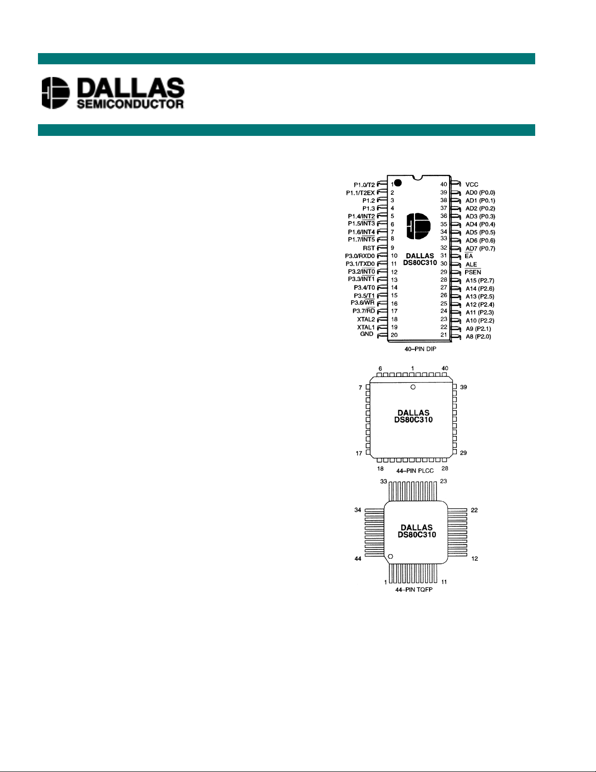
Available in 40-pin PDIP, 44-pin PLCC, and
44-pin TQFP
PACKAGE OUTLINE
DESCRIPTION
The DS80C310 is a fast 80C31/80C32-compatible microcontroller. It features a redesigned processor
core without wasted clock and memory cycles. As a result, it executes every 8051 instruction between 1.5
and 3 times faster than the original architecture for the same crystal speed. Typical applications will see a
speed improvement of 2.5 times using the same code and the same crystal. The DS80C310 offers a
maximum crystal speed of 33 MHz, resulting in apparent execution speeds of 82.5 MHz (approximately
2.5X).
1 of 23 112299
Page 2
DS87C520/DS83C520
The DS80C310 is pin-compatible with the standard 80C32 and includes standard resources such as three
timer/counters, 256 bytes of RAM, and a serial port. It also provides dual data pointers (DPTRs) to speed
block data memory moves. It also can adjust the speed of MOVX data memory access between two and
nine machine cycles for flexibility in selecting external memory and peripherals. The DS80C310 offers
upward compatibility with the DS80C320.
ORDERING INFORMATION:
PART
NUMBER
DS80C310-MCG
DS80C310-QCG
DS80C310-ECG
DS80C310-MCL
DS80C310-QCL
DS80C310-ECL
PACKAGE MAX. CLOCK SPEED
40-pin plastic DIP
44-pin PLCC
44-pin TQFP
40-pin plastic DIP
44-pin PLCC
44-pin TQFP
25 MHz
25 MHz
25 MHz
33 MHz
33 MHz
33 MHz
TEMPERATURE
RANGE
0°C to 70°C
0°C to 70°C
0°C to 70°C
0°C to 70°C
0°C to 70°C
0°C to 70°C
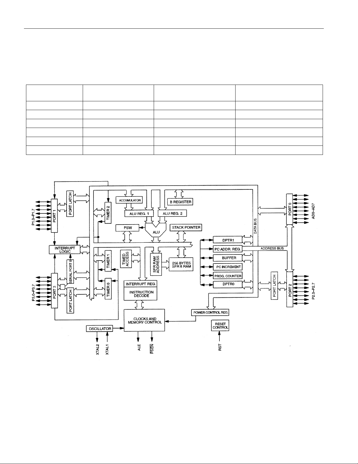
DS80C310 BLOCK DIAGRAM Figure 1
2 of 23
Page 3
DS87C520/DS83C520
PIN DESCRIPTION Table 1
DIP PLCC TQFP SIGNAL
NAME
40 44 38 V
20 22,23116,17,
GND GND- Digital circuit ground.
CC
VCC -+5V.
39
910 4 RSTRST - Input. The RST input pin contains a Schmitt voltage
input to recognize external active high reset inputs. The pin
also employs an internal pulldown resistor to allow for a
combination of wired OR external Reset sources.
18
19
20
21
14
15
XTAL2
XTAL1
XTAL1, XTAL2 - The crystal oscillator pins XTAL1 and
XTAL2 provide support for parallel resonant, AT cut
crystals. XTAL1 acts also as an input in the event that an
external clock source is used in place of a crystal. XTAL2
serves as the output of the crystal amplifier.
29 32 26
PSEN PSEN - Output. The Program Store Enable output. This
signal is commonly connected to external ROM memory as a
chip enable.
PSEN is active low. PSEN is driven high
when data memory (RAM) is being accessed through the bus
and during a reset condition.
30 33 27 ALE ALE - Output. The Address Latch Enable output functions
as clock to latch the external address LSB from the
multiplexed address/data bus on Port 0. This signal is
commonly connected to the latch enable of an external 373
family transparent latch.ALE is forced high when the
DS80C310 is in a Reset condition.
39
38
37
36
35
34
33
32
43
42
41
40
39
38
37
36
37
36
35
34
33
32
31
30
1-8 2-9 40-44
1-3
AD0 (P0.0)
AD1 (P0.1)
AD2 (P0.2)
AD3 (P0.3)
AD4 (P0.4)
AD5 (P0.5)
AD6 (P0.6)
AD7 (P0.7)
AD0-7 (Port 0) - I/O. Port 0 is the multiplexed address/data
bus. During the time when ALE is high, the LSB of a
memory address is presented. When ALE falls to a logic 0,
the port transitions to a bidirectional data bus. This bus is
used to read external ROM and read/write external RAM
memory or peripherals. Port 0 has no true port latch and can
not be written directly by software. The reset condition of
Port 0 is high.
P1.0-P1.7 Port 1 - I/O. Port 1 functions as both an 8-bit bidirectional
I/O port and an alternate functional interface for Timer 2 I/O
and new External Interrupts. The reset condition of Port 1 is
with all bits at a logic 1. In this state, a weak pullup holds the
port high. This condition also serves as an input mode, since
any external circuit that writes to the port will overcome the
weak pullup. When software writes a 0 to any port pin, the
DS80C310 will activate a strong pulldown that remains on
until either a 1 is written or a reset occurs. Writing a 1 after
the port has been at 0 will cause a strong transition dr iver to
turn on, followed by a weaker sustaining pullup. Once the
momentary strong driver turns off, the port once again
becomes the output high (and input) state. The alternate
modes of Port 1 are outlined as follows:
DESCRIPTION
3 of 23
Page 4
DS87C520/DS83C520
DIP PLCC TQFP SIGNAL
NAME
1
2
3
4
5
6
7
8
21
22
23
24
25
26
27
28
10-17
2
3
4
5
6
7
8
9
24
25
26
27
28
29
30
31
11,
40
41
42
43
44
1
2
3
18
19
20
21
22
23
24
25
5,7-13
A8 (P2.0)
A9 (P2.1)
A10(P2.2)
A11(P2.3)
A12(P2.4)
A13 P2.5)
A14(P2.6)
A15(P2.7)
P3.0-3.7 Port 3 - I/O. Port 3 functions as both an 8-bit bidirectional I/O
13-19
10
11
12
13
14
15
16
17
11
13
14
15
16
17
18
19
31 35 29
-12346
5
7
8
9
10
11
12
13
EA
NC NC - Reserved. These pins should not be connected. They
28
DESCRIPTION
Port Alternate Function
P1.0 T2 External I/O for Timer/Counter 2
P1.1 T2EX Timer/Counter 2 Capture/Reload Trigger
P1.2 none (DS80C320 has a serial port RXD)
P1.3 none (DS80C320 has a serial port TXD)
P1.4 INT2 External Interrupt 2 (Positive Edge Detect)
P1.5
INT3 External Interrupt 3 (Negative Edge Detect)
P1.6 INT4 External Interrupt 4 (Positive Edge Detect)
P1.7
INT5 External Interrupt 5 (Negative Edge Detect)
A8-15 (Port 2) -Output. Port 2 serves as the MSB for external
addressing. P2.7 is A15 and P2.0 is A8. The DS80C310 will
automatically place the MSB of an address on P2 for external
ROM and RAM access. Although Port 2 can be accessed like
an ordinary I/O port, the value stored on the Port 2 latch will
never be seen on the pins (due to memory access). Therefore
writing to Port 2 in software is only usef ul for the instructions
MOVX A, @ Ri or MOVX @ Ri, A. These instructions use the
Port 2 internal latch to supply the external address MSB; the
Port 2 latch value will be supplied as the address information.
port and an alternate functional interface for external Interrupts,
Serial Port 0, Timer 0 and 1 Inputs,
RD and WR strobes. The
reset condition of Port 3 is with all bits at a logic 1. In this
state, a weak pullup holds the port high. This condition also
serves as an input mode, since any external circuit that writes
to the port will overcome the weak pullup. When software
writes a 0 to any port pin, the DS80C310 will activate a strong
pulldown that remains on until either a 1 is written or a reset
occurs. Writing a 1 after the port has been at 0 will cause a
strong transition driver to turn on, followed by a weaker
sustaining pullup. Once the momentary strong driver turns off,
the port once again becomes both the output high and input
state. The alternate modes of Port 3 are outlined below.
Port Alternate Mode
P3.0 RXD0 Serial Port 0 Input
P3.1 TXD0 Serial Port 0 Output
P3.2
P3.3
INT0 External Interrupt 0
INT1 External Interrupt 1
P3.4 T0 Timer 0 External Input
P3.5 T1 Timer 1 External Input
P3.6
P3.7
WR External Data Memory Write Strobe
RD External Data Memory Read Strobe
EA - Input. This pin must be connected to ground for proper
operation.
are reserved for use with future devices in this family.
4 of 23
Page 5

DS87C520/DS83C520
COMPATIBILITY
The DS80C310 is a fully static CMOS 8051-compatible microcontroller designed for high p erformance.
In most cases the DS80C310 can drop into an existing socket for the 80C31 or 80C32 to improve the
operation significantly. In general, software written for existing 8051-based systems works without
modification on the DS80C310. The exception is critical timing since the High-Speed Micro performs its
instructions much faster than the original for any given crystal selection. The DS80C310 runs the
standard 8051 family instruction set and is pin compatible with DIP, PLCC or TQFP packages. The
DS80C310 is a streamlined version of the DS80C320. It maintains upward compatibility but has fewer
peripherals.
The DS80C310 provides three 16-bit timer/counters, a full-duplex serial port, and 256 bytes of direct
RAM. I/O ports have the same operation as a standard 8051 product. Timers will default to a 12-clock per
cycle operation to keep their timing compatible with original 8051 family systems. However, timers are
individually programmable to run at the new 4 clocks per cycle if desired.
The DS80C310 provides several new hardware functions that are controlled by Special Function
registers. A summary of the Special Function Registers is provided in Table 2.
PERFORMANCE OVERVIEW
The DS80C310 features a high-speed 8051 compatible core. Higher spe ed comes not just from incr easin g
the clock frequency, but from a newer, more efficient design.
This updated core does not have the dummy memory cycles that are present in a standard 8051. A
conventional 8051 generates machine cycles using the clock frequenc y divided by 12. In the DS80C310,
the same machine cycle takes four clocks. Thus the fastest instructi on, 1 machine cycle, executes three
times faster for the same crystal frequency. Note that these are identical instructions. The majority of
instructions on the DS80C310 will see the full 3 to 1 speed improvement. Some instructions will get
between 1.5 and 2.4 to 1 improvement. All instructions are faster than the original 8051.
The numerical average of all opcodes gives approximately a 2.5 to 1 speed improvement. Improvement of
individual programs will depend on the actual instructions used. Speed-sensitive applications would make
the most use of instructions that are three times faster. However, the sheer number of 3 to 1 improved
opcodes makes dramatic speed improvements likely for any code. These archite cture improvements and
0.8
µm CMOS produce a peak instruction cycle in 121 ns (8.25 MIPs). The Dual Data Pointer feature
also allows the user to eliminate wasted instructions when moving blocks of memory.
INSTRUCTION SET SUMMARY
All instructions in the DS80C310 perform the same functions as their 8051 counterparts. Their effect on
bits, flags, and other status functions is identical. However, the timing of each instruction is different.
This applies both in absolute and relative number of clocks.
For absolute timing of real time events, the timing of software loops can be calculated using a table in the
High-Speed Microcontroller User’s Guide. However, counter/timers default to run at the older 12 clocks
per increment. In this way, t imer-based events occur at the standard intervals with software executing at
higher speed. Timers optionally can run at 4 clocks per increment to take advantage of faster processor
operation.
The relative time of two instructions might be different in the new architecture than it was previously. For
example, in the original architecture the “MOVX A, @ DPTR” i nstruction and the “MOV direct , direct”
instruction used two machine cycles or 24 oscillator cycles. Therefore, they required the same amount of
5 of 23
Page 6

DS87C520/DS83C520
time. In the DS80C310, the MOVX instruction takes as little as two machine cycles or eight oscillator
cycles but the “MOV direct, direct” uses three machine cycles or 12 oscillator cycles. While both are
faster than their original counterparts, they now have different execution times. This is because the
DS80C310 usually uses one instruction cycle for each instruction byte. The user concerned with precise
program timing should examine the timing of each instruction for familiarity with the changes. Note that
a machine cycle now requires just four clocks, and provides one ALE pulse per cycle. Many instructions
require only one cycle, but some require five. In the original architecture, all were one or two cycles
except for MUL and DIV. Refer to the High-Speed Microcontroller User’s Guide for details and
individual instruction timing.
6 of 23
Page 7
DS87C520/DS83C520
SPECIAL FUNCTION REGISTERS
Special Function Registers (SFRs) control most special features of the DS80C310. The High-Speed
Microcontroller User’s Guide describes all SFRs. Functions that are not part of the standa rd 80C32 are in
bold.
SPECIAL FUNCTION REGISTERS Table 2
REGISTER BIT 7 BIT 6 BIT 5 BIT 4 BIT 3 BIT 2 BIT 1 BIT 0 ADDRESS
SP
DPL
DPH
DPL1
DPH1
DPS
PCON SMOD SM0D0 - - GF1 GF0 STOP IDLE
TCON TF1 TR1 TF0 TR0 IE1 IT1 IE0 IT0
TMOD GATE
TL0
TL1
TH0
TH1
CKCON - - T2M T1M T0M MD2 MD1 MD0
P1 P1.7 P1.6 P1.5 P1.4 P1.3 P1.2 P1.1 P1.0
EXIF IE5 IE4 IE3 IE2
SCON SMO/FE SM1 SM2 REN TB8 RB8 TI RI
SBUF
P2 P2.7 P2.6 P2.5 P2.4 P2.3 P2.2 P2.1 P2.0
IE EA - ET2 ES0 ET1 EX1 ET0 EX0
SADDR0
P3 P3.7 P3.6 P3.5 P3.4 P3.3 P3.2 P3.1 P3.0
IP - - PT2 PSO PT1 PX1 PT0 PX0
SADEN0
STATUS 0 HIP LIP 1 1 1 1 1
T2CON TF2 EXF2 RCLK TCLK EXEN2 TR2
T2MOD - - - - - - T2OE DCEN
RCAP2L
RCAP2H
TL2
TH2
PSW CY AC F0 RS1 RS0 OV FL P
WDCON
ACC
EIE
B
EIP
0000000SEL
C/
T
M1 M0 GATE
C/
T
M1 M0
----
T2 CP/RL2
C/
-
POR
----
----
-- --- -
EX5 EX4 EX3 EX2
PX5 PX4 PX3 PX2
7 of 23
Page 8

DS87C520/DS83C520
MEMORY ACCESS
The DS80C310 contains no on-chip ROM, and 256 bytes of scratchpad RAM. Off-chip memory is
accessed using the multiplexed address/data bus on P0 and the MSB address on P2. Timing diagrams are
provided in the Electrical Specifications. Program memory (ROM) is accessed at a fixed rate dete rmined
by the crystal frequency and the actual instructions. As mentioned above, an instruction cycle requires
four clocks. Data memory (RAM) is accessed according to a variable speed MOVX instruction as
described below.
STRETCH MEMORY CYCLE
The DS80C310 allows the application software to adjust the speed of data memory access. The micro is
capable of performing the MOVX in as few as two instruction cycles. However, this value can be
stretched as needed so that both fast memory and slow memory or peripherals can be accessed with no
glue logic. Even in highspeed systems, it may not be necessary or desirable to perform data memory
access at full speed. In addition, there a re a variet y of memory mapped periphe rals such as LCD displa ys
or UARTs that are not fast.
The Stretch MOVX is controlled b y the Clock Control Register at SFR locati on 8Eh as described below.
This allows the user to select a stretch value between 0 and 7. A Stretch of 0 will result in a two-machine
cycle MOVX. A Stretch of 7 will result in a MOVX of nine machine cycles. Software can dynamically
change this value depending on the particular memory or peripheral.
On reset, the Stretch value will default to a one resulting in a three-cycle MOVX. Therefore, RAM a ccess
will not be performed at full speed. This is a convenience to existing designs that may not have fast RAM
in place. When maximum speed is desired, the software should select a Stretch value o f 0. When using
very slow RAM or peripherals, a larger stretch value can be selected. Note that this affects data memory
only and the only way to slow program memory (ROM) access is to use a slower crystal.
Using a Stretch value between 1 and 7 causes the microcontroller to stretch the read/write strobe and all
related timing. This results in a wider read/write strobe allowing more time for memory/peripherals to
respond. The timing of the variable speed MOVX is shown in the Electrical Specifications. Note that full
speed access is not the reset default case. Table 3 shows the resulting strobe widths for each Stretch value.
The memory stretch is implemented using the Clock Control Special Function Register at SFR location
8Eh. The stretch value is selected using bits CKCON.2-0. In the table, these bits are referred to as M2
through M0. The first stretch (default) allows the use of common 120 ns or 150 ns RAMs without
dramatically lengthening the memory access.
DATA MEMORY CYCLE STRETCH VALUES Table 3
CKCON.2-0 RD OR WR STROBE STROBE WIDTH TIME
M2 M1 M0 MEMORY CYCLES WIDTH IN CLOCKS @ 25 MHz @ 33 MHz
0 0 0 2 2 80 ns 60ns
0 0 1 3(default) 4 160 ns 121ns
0 1 0 4 8 320 ns 242ns
0 1 1 5 12 480 ns 364ns
1 0 0 6 16 640 ns 485ns
1 0 1 7 20 800 ns 606ns
1 1 0 8 24 960 ns 727ns
1 1 1 9 28 1120 ns 848ns
8 of 23
Page 9

DS87C520/DS83C520
DUAL DATA POINTER
Data memory block moves can be accelerated using the DS80C310 Dual Data Pointer (DPTR). The
standard 8032 DPTR is a 16-bit value that is used to address off-chip data RAM o r peripherals. In the
DS80C310, the standard data pointer is called DPTR and is located at SFR addresses 82h and 83h. The se
are the standard locations. No modification of standard code is needed to use DPTR. The new DPTR is
located at SFR 84h and 85h and is called DPTR1. The DPTR Select bit (DPS) chooses the active pointer
and is located at the lsb of the SFR location 86h. No other bits in register 86h have any effect and ar e set
to 0. The user switches between data pointers by toggling the lsb of register 86h. The increment (INC)
instruction is the fastest way to accomplish this. All DPTR-related instructions use the currently selected
DPTR for any activity. Therefore only one instruction is required to switch from a source to a destination
address. Using the Dual Data Pointer saves code from needing to save source and destination addresses
when doing a block move. Once loaded, the software simply switches between DPTR0 and 1. The
relevant register locations are as follows.
DPL 82h Low byte original DPTR
DPH 83h High byte original DPTR
DPL1 84h Low byte new DPTR
DPH1 85h High byte new DPTR
DPS 86h DPTR Select (lsb)
STOP MODE ENHANCEMENTS
Setting bit 1 of the Power Control register (PCON; 87h) invokes the Stop mode. Stop mode is the lowest
power state since it turns off all internal clocki n g. The I
(but is specified in the Electrical Specifications). The CPU will exit Stop mode from an external interrupt
or a reset condition. Internally generated interrupts are not useful since they require clocking activity.
The DS80C310 allows a resume from Stop using an INT2-5, which are edge-triggered interrupts. The
start-up timing is managed by an internal crystal counter. A delay of 65,536 clocks occurs to give the
crystal enough time to start and stabilize.
of a standard Stop mode is approximately 1 µA
CC
PERIPHERAL OVERVIEW
The DS80C310 provides the same peripheral functions as the standard 80C32. It is compatible with the
DS80C320 but does not offer all of the peripherals.
TIMER RATE CONTROL
There is one important difference between the DS80C310 and 8051 regarding timers. The original 8051
used 12 clocks per cycle for timers as well as for machine cycles. The DS80C310 architecture normall y
uses 4 clocks per machine cycle. However, in the area of timers and serial ports, the DS80C310 will
default to 12 clocks per cycle on reset. This allows existing code with real-time dependencies such as
baud rates to operate properly.
If an application needs higher speed timers or serial baud rates, the user can select individual timers to run
at the 4-clock rate. The Clock Cont rol register (CKCON; 8Eh) determines thes e timer speeds. When t he
relevant CKCON bit is a logic 1, the DS80C310 uses 4 clocks per cycle to generate timer speeds. When
the bit is a 0, the DS80C310 uses 12 clocks for timer speeds. The reset condition is a 0. CKCON.5 selects
the speed of Timer 2. CKCON.4 selects Timer 1 and CKCON.3 selects Timer 0. Note that unless a user
desires very fast timing, it is unnecessary to alter these bits. Note that the timer controls are independent.
9 of 23
Page 10

DS87C520/DS83C520
POWER ON RESET
The DS80C310 will hold itself in reset during a power-up until 65,536 clock cycles have elapsed. The
power-on reset used by the DS80C310 differs somewhat from other members of the High-Speed
Microcontroller family. The crystal oscillator may start anywhere between 1.0V and 4.5V but is not
specified. This eliminates the need for an RC reset circuit. For voltage-specific precision brownout
detection, an external component will be needed. When the device goes through a power-on reset, the
POR flag will be set in the WDCO N (D8h) register at bit 6.
INTERRUPTS
The DS80C310 provides 10 interrupt sources with two priority levels. Software can assign high or low
priority to all sources. All interrupts that are new to the 8051 have a lower natural priority than the
originals.
INTERRUPT SOURCES AND PRIORITIES Table 4
NAME DESCRIPTION VECTOR
INT0
TF0 Timer 0 0Bh 2
INT1
TF1 Timer 1 1Bh 4
SCON T1 or R1 from the serial port 23h 5
TF2 Timer 2 2Bh 6
INT2 External Interrupt 2 43h 7
INT3
INT4 External Interrupt 4 53h 9
INT5
External Interrupt 0 03h 1
External Interrupt 1 13h 3
External Interrupt 3 4Bh 8
External Interrupt 5 5Bh 10
NATURAL
PRIORITY
10 of 23
Page 11

DS87C520/DS83C520
ABSOLUTE MAXIMUM RATINGS*
Voltage on Any Pin Relative to Ground -0.3V to +7.0V
Operating Temperature 0
Storage Temperature -55
Soldering Temperature 260
°C to 70°C
°C to +125°C
°C for 10 seconds
∗ This is a stress rating only and functional operation of the device at these or any other conditions
above those indicated in the operation sections of this specification is not implied. Exposure to
absolute maximum rating conditions for extended per iods of time may affect reliability.
DC ELECTRICAL CHARACTERISTICS
PARAMETER SYMBOL MIN TYP MAX UNITS NOTES
Supply Voltage V
Supply Current Active Mode
@ 33 MHz
Supply Current Idle Mode
@ 33 MHz
Supply Current Stop Mode
I
I
IDLE
I
STOP
Input Low Level V
Input High Level (Except
XTAL1 and RST)
V
Input High Level XTAL1 and RST V
Output Low Voltage Ports 1,3
@ I
= 1.6 mA
OL
V
Output Low Voltage Port 0,2,
V
ALE,
PSEN @ I
=3.2 mA
OL
Output High Voltage Port 1, 3,
V
ALE,
PSEN @ I
Output High Voltage
@ I
=-1.5mA Ports 1,3
OH
=-50 µA
OH
V
Output High Voltage Port 0, 2,
V
ALE,
PSEN @ I
=-8 mA
OH
Input Low Current Ports 1, 3
@ 0.45V
Transition Current from 1 to 0
Ports 1,3 @ 2V
I
Input Leakage Port 0, Bus Mode
RST Pulldown Resistance
R
CC
CC
IH2
OL1
OL2
OH1
OH2
OH3
I
IL
TL
I
L
RST
IL
IH
4.0 5.0 5.5 V 1
30 mA 2
15 mA 3
1
µA
-0.3 +0.8 V 1
2.0 VCC+0.3 V 1
3.5 VCC+0.3 V 1
0.15 0.45 V 1
0.15 0.45 V 1, 5
2.4 V 1, 6
2.4 V 1, 7
2.4 V 1, 5
-55
-650
-300 300
50 170
µA
µA
µA
K
Ω
10
4
8
9
NOTES FOR DC ELECTRICAL CHARACTERISTICS:
All parameters apply to both commercial and industrial temperature operation unless otherwise noted.
1.
All voltages are referenced to ground.
2.
Active current is measured with a 33 MHz clock source driving XTAL1, V
pins disconnected.
11 of 23
=RST=5.5V, all other
CC
Page 12

DS87C520/DS83C520
3.
Idle mode current is measured with a 33 MHz clock source driving XTAL1, V
=5.5V, RST at
CC
ground, all other pins disconnected.
4.
Stop mode current measured with XTAL1 and RST grounded, V
=5.5V, all other pins
CC
disconnected.
5.
When addressing external memory.
6.
RST=V
7.
During a 0 to 1 transition, a one-shot drives the ports hard for two clock cycles. This measurement
. This condition mimics operation of pins in I/O mode.
CC
reflects port in transition mode.
8.
Ports 1 and 3 source transition current when being pulled down externally. It reaches its m aximum at
approximately 2V.
9.
0.45<V
<VCC. Not a high-impedance input. This port is a weak address holding latch because Port 0
IN
is dedicated as an address bus on the DS80C310. Peak current occurs near the input transition point of
the latch, approximately 2V.
10.
Current required from external circuit to hold a logic low level on an I/O pin while the corresponding
port latch bit is set to 1. This is only the current required to hold the low level; transitions from 1 to 0
on an I/O pin will also have to overcome the transition current.
TYPICAL I
VERSUS FREQUENCY Figure 2
CC
12 of 23
Page 13

AC ELEC TRICAL CHAR ACTERI STICS
L
L
L
L
PARAMETER SYMBOL
Oscillator Freq. (Ext. Osc.)
(Ext. Crystal)
ALe Pulse Width t
Port 0 Address Valid to ALE Low t
Address Hold after ALE Low t
ALE Low to Valid Instruction In t
ALE Low to PSEN Low
PSEN Pulse Width
PSEN Low to Valid Instr. In
Input Instruction Hold after PSEN
Input Instruction Float after PSEN
Port 0 Address to Valid Instr. In t
Port 2 Address to Valid Instr. In t
PSEN Low to Address Float
1/t
LHLL
AVLL
LLAX1
LLIV
t
LLPL
t
PLPH
t
PLIV
t
PXIX
t
PXIZ
AVIV
AVIV2
t
PLAZ
CLCL
DS87C520/DS83C520
25 MHz VARIABLE CLOCK
MIN MAX MIN MAX
0
1
40 1.5t
10 0.5t
10 0.5t
10 0.5t
55 2t
33
33
0
1
-5 ns
CLC
-5 ns
CLC
-5 ns
CLC
56 2.5t
-5 ns
CLC
-5 ns
CLCL
41 2t
33
33
CLCL
CLCL
-20 ns
NOTES
MHz
-20 ns
00 ns
26 t
71 3t
81 3.5t
-5 ns
CLCL
-20 ns
CLCL
-25 ns
CLCL
00ns
NOTES FOR AC ELECTRICAL CHARACTERISTICS
All parameters apply to both commercial and industrial temperature range operation unless otherwise
noted. All signals
100 pF. Interfacing to
This will not damage the parts, but
50% duty cycle for the oscillator. Port 2 and ALE
characterized with load capacitance of 80 pF except Po rt 0, A LE, PSEN , and WR with
memory devices with float times (turn off times) over 25 ns ma y cause contention.
will cause an increase in operating current. Specifications assume a
timing will change in relation to duty cycle variation.
13 of 23
Page 14

MOVX CHARACTERISTICS
PARAMETER SYMBOL
Data Access ALE Pulse Width
Address Hold after ALE Low for
MOVX Write
RD Pulse Width
WR Pulse Width
RD Low to Valid Data In
Data Hold after Read t
Data Float after Read
ALE Low to Valid Data In
Port 0 Address to Valid Data In
Port 2 Address to Valid Data In
ALE Low to RD or WR Low
Port 0 Address to RD or WR Low
Port 2 Address to RD or WR Low
Data Valid to WR Transition
Data Hold after Write
RD Low to Address Float
RD or WR High to ALE High
t
LHLL2
t
LLAX2
t
RLRH
t
WLWH
t
RLDV
RHDX
t
RHDZ
t
LLDV
t
AVDV1
t
AVDV2
t
LLWL
t
AVWL1
t
AVWL2
t
QVWX
t
WHQX
t
RLAZ
t
WHLH
DS87C520/DS83C520
VARIABLE CLOCK
MIN MAX
1.5t
2t
0.5t
t
2t
t
2t
t
CLCL
CLCL
CLCL
CLCL
CLCL
MCS
CLCL
MCS
-5
-5
-5
-5
-5
-10
-5
-10
2t
t
CLCL
MCS
-20
-20
UNITS STRETCH
=0
t
ns
ns
ns
ns
ns
MCS
t
MCS
t
MCS
t
MCS
t
MCS
t
MCS
t
MCS
t
MCS
t
MCS
t
MCS
>0
=0
>0
=0
>0
=0
>0
=0
>0
0ns
t
0.5t
t
t
2t
1.5t
2.5t
CLCL
CLCL
CLCL
CLCL
CLCL
CLCL
-5
-5
-5
-5
-10
-10
CLCL
2t
CLCL
2.5t
CLCL
t
CLCL+tMCS
3t
CLCL
1.5t
CLCL+ tMCS
20
3.5t
CLCL
2t
CLCL+ tMCS
0.5t
CLCL
t
CLCL
-5
-5
-20
-20
-20
+5
-40
+5
-20
ns
ns
-
ns
ns
ns
ns
ns
t
MCS
t
MCS
t
MCS
t
MCS
t
MCS
t
MCS
t
MCS
t
MCS
t
MCS
t
MCS
t
MCS
t
MCS
t
MCS
t
MCS
=0
>0
=0
>0
=0
>0
=0
>0
=0
>0
=0
>0
=0
>0
-5 ns
t
2t
t
CLCL
CLCL
0
CLCL
-5
-5
-5
-0.5t
t
CLCL
-5 ns
CLCL
10
+5
ns
ns
t
MCS
t
MCS
t
MCS
t
MCS
=0
>0
=0
>0
NOTE: t
value of t
M2 M1 M0 MOVX CYCLES t
is a time period related to the Stretch memory cycle selection. The following table shows the
MCS
for each Stretch selection.
MCS
MCS
0 0 0 2 machine cycles 0
0 0 1 3 machine cycles (default) 4 t
0 1 0 4 machine cycles 8 t
0 1 1 5 machine cycles 12 t
1 0 0 6 machine cycles 16 t
1 0 1 7 machine cycles 20 t
1 1 0 8 machine cycles 24 t
1 1 1 9 machine cycles 28 t
14 of 23
CLCL
CLCL
CLCL
CLCL
CLCL
CLCL
CLCL
Page 15

DS87C520/DS83C520
L
L
EXTERNAL CLOCK CHARACTERISTICS
PARAMETER SYMBOL MIN TYP MAX UNITS NOTES
Clock High Time t
Clock Low Time t
Clock Rise Time t
Clock Fall Time t
CHCX
CLCX
CLCL
CHCL
10 ns
10 ns
5ns
5ns
SERIAL PORT MODE 0 TIMING CHARACTERISTICS
PARAMETER SYMBOL MIN TYP MAX UNITS NOTES
Serial Port Clock Cycle Time
SM2=0, 12 clocks per cycle
SM2=1, 4 clocks per cycle
Output Data Setup to Clock
Rising
SM2=0, 12 clocks per cycle
SM2=1, 4 clocks per cycle
Output Data Hold from
Clock Rising
SM2=0, 12 clocks per cycle
SM2=1, 4 clocks per cycle
Input Data Hold after Clock
Rising
SM2=0, 12 clocks per cycle
SM2=1, 4 clocks per cycle
Clock Rising Edge to Input
Data Valid
SM2=0, 12 clocks per cycle
SM2=1, 4 clocks per cycle
t
XLXL
t
QVXH
t
XHQX
t
XHDX
t
XHDV
12t
4t
10t
3t
2t
t
t
t
11t
3t
CLC
CLCL
CLCL
CLC
CLCL
CLCL
CLCL
CLCL
CLCL
CLCL
ns
ns
ns
ns
ns
ns
ns
ns
ns
ns
EXPLANATION OF AC SYMBOLS
In an effort to remain compatible with the original 8051 family, this device specifies the same parameters
as such devices, using the same symbols. For completeness, the following is an explanation of the
symbols.
t Time
A Address
C Clock
D Input data
H Logic level high
L Logic level low
I Instruction
P
Q Output data
R
V Valid
W
X No longer a valid logic level
Z Tristate
PSEN
RD signal
WR signal
15 of 23
Page 16

EXTERNAL PROGRAM MEMORY READ CYCLE
DS87C520/DS83C520
EXTERNAL DATA MEMORY READ CYCLE
16 of 23
Page 17

DATA MEMORY WRITE CYCLE
DS87C520/DS83C520
DATA MEMORY WRITE WITH STRETCH=1
17 of 23
Page 18

DATA MEMORY WRITE WITH STRETCH=2
DS87C520/DS83C520
EXTERNAL CLOCK DRIVE
18 of 23
Page 19

SERIAL PORT MODE 0 TIMING
SERIAL PORT 0 (SYNCHRONOUS MODE)
HIGH-SPEED OPERATION SM2=1=>TXD CLOCK=XTAL/4
DS87C520/DS83C520
19 of 23
Page 20

40-PIN PDIP (600-MIL)
DS87C520/DS83C520
PKG 40-PIN
DIM MIN MAX
A - 0.200
A1 0.015 A2 0.140 0.160
b 0.014 0.022
c 0.008 0.012
D 1.980 2.085
E 0.600 0.625
E1 0.530 0.555
e 0.090 0.110
L 0.115 0.145
eB 0.600 0.700
ALL DIMENSIONS ARE IN INCHES.
20 of 23
Page 21

44-PIN PLCC
DS87C520/DS83C520
PKG 44-PIN
DIM MIN MAX
A 0.165 0.180
A1 0.090 0.120
A2 0.020 -
B 0.026 0.033
B1 0.013 0.021
c 0.009 0.012
CH1 0.042 0.048
D 0.685 0.695
D1 0.650 0.656
D2 0.590 0.630
E 0.685 0.695
E1 0.650 0.656
E2 0.590 0.630
e1 0.050 BSC
N44 -
21 of 23
Page 22

44-PIN TQFP
DS87C520/DS83C520
22 of 23
Page 23

DS87C520/DS83C520
PKG 44-PIN
DIM MIN MAX
A - 1.20
A1 0.05 0.15
A2 0.95 1.05
D 11.80 12.20
D1 10.00 BSC
E 11.80 12.20
E1 10.00 BSC
L 0.45 0.75
e 0.80 BSC
B 0.30 0.45
C 0.09 0.20
56-G4012-001
DATA SHEET REVISION SUMMARY
The following represent the key differences between 02/19/98 and 09/01/98 version of the DS80C310
data sheet. Please review this summary carefully.
1.
Add note to clarify I
2.
Change serial port mode 0 timing diagram label from t
3.
Changed minimum oscillator frequency to 1 MHz when using external crystal.
4.
Corrected “Data memory write with stretch” diagrams to show falling edge of ALE coincident with
specification.
IL
QVXL
to t
QVXH
.
rising edge of C3 clock.
23 of 23
 Loading...