

Page 1
DS78C20/DS88C20
Dual CMOS Compatible Differential Line Receiver
DS78C20/DS88C20 Dual CMOS Compatible Differential Line Receiver
May 1998
General Description
The DS78C20 and DS88C20 are high performance, dual differential, CMOS compatible line receivers for both balanced
and unbalanced digital data transmission. The inputs are
compatible with EIA and Federal Standards.
Input specifications meet or exceed those of the popular
DS7820/DS8820 line receiver, and the pinout is identical.
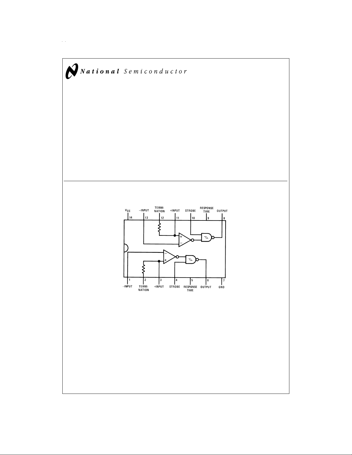
A response pin is provided for controlling sensitivity to input
noise spikes with an external capacitor. Each receiver includes a 180Ω terminating resistor, which may be used optionally on twisted pair lines. The DS78C20 is specified over
a −55˚C to +125˚C operating temperature range, and the
DS88C20 over a 0˚C to +70˚C range.
Connection Diagram
Dual-In-Line Package
Features
n Meets requirements of EIA Standards RS-232-C RS-422
and RS-423, and Federal Standards 1020 and 1030
n Input voltage range of
common-mode)
n Separate strobe input for each receiver
1
n
⁄2VCCstrobe threshold for CMOS compatibility
n 5k typical input impedance
n 50 mV input hysteresis
n 200 mV input threshold
n Operation voltage range=4.5V to 15V
n DS7830/DS8830 recommended driver
±
15V (differential or
DS005798-1
Top View
Order Number DS88C20N
See NS Package Numbers N14A
For Complete Military Product Specifications,
refer to the appropriate SMD or MDS.
Order Number DS78C20J/883
See NS Package Number J14A
© 1998 National Semiconductor Corporation DS005798 www.national.com
Page 2

Absolute Maximum Ratings (Note 2)
If Military/Aerospace specified devices are required,
please contact the National Semiconductor Sales Office/
Distributors for availability and specifications.
Supply Voltage 18V
Common-Mode Voltage
Differential Input Voltage
Strobe Voltage 18V
Output Sink Current 50 mA
Maximum Power Dissipation (Note 1) at 25˚C
Cavity Package 1364 mW
±
25V
±
25V
Lead Temperature (Soldering, 4 seconds) 260˚C
Operating Conditions
Supply Voltage (V
Temperature (T
) 4.5 15 V
CC
)
A
DS78C20 −55 +125 ˚C
DS88C20 0 +70 ˚C
Common-Mode Voltage (V
Note 1: Derate cavity package 9.1 mW/˚C; derate molded package 10.2
mW/˚C above 25˚C.
Min Max Units
) −15 +15 V
CM
Molded Package 1280 mW
Storage Temperature Range −65˚C to
+150˚C
Electrical Characteristics (Notes 3, 4)
Symbol Parameter Conditions Min Typ Max Units
V
R
R
I
V
V
V
I
I
I
V
V
I
Differential Threshold I
TH
Voltage V
Input Resistance −15V ≤ VCM≤ 15V 5 kΩ
IN
Line Termination
T
Resistance
Data Input Current V
IND
(Unterminated) V
Input Balance I
THB
Logical “1” Output Voltage I
OH
Logical “0” Output Voltage I
OL
Power Supply Current 15V ≤ VCM≤ −15V, V
CC
Logical “1” Strobe Input
IN(1)
Current
Logical “0” Strobe Input
IN(0)
Current
Logical “1” Strobe Input I
IH
Voltage V
Logical “0” Strobe Input I
IL
Voltage V
Output Short-Circuit
OS
Current
=
−200 µA, −10V ≤ V
OUT
≥ VCC−1.2V −15V ≤ VCM≤ 15V 0.06 0.3 V
OUT
=
I
OUT
1.6 mA, V
≤ 0.5V −10V ≤ VCM≤ 10V −0.08 −0.2 V
OUT
−15V ≤ V
=
T
25˚C 100 180 300 Ω
A
=
10V 2 3.1 mA
CM
=
0V 0 −0.5 mA
CM
=
V
−10V −2 −3.1 mA
CM
OUT
V
CC
=
200 µA, V
−1.2V, R
≥ −7V ≤ VCM≤ 7V
OUT
=
500Ω, 0.1 0.4 V
S
≤ 10V 0.06 0.2 V
CM
≤ 15V −0.08 −0.3 V
CM
(Note 6)
=
I
1.6 mA, V
OUT
=
R
500Ω, (Note 6)
S
=
−200 µA, V
OUT
=
1.6 mA, V
OUT
=
V
−0.5V V
DIFF
≤ 0.5V, −7V ≤ VCM≤ 7V −0.1 −0.4 V
OUT
=
1V V
DIFF
=
−1V 0.25 0.5 V
DIFF
=
5.5V 8 15 mA
CC
=
15V 15 30 mA
CC
−1.2 VCC−0.75 V
CC
(Both Receivers)
=
V
STROBE
V
STROBE
OUT
OUT
OH
V
15V, V
=
0V, V
=
1.6 mA, V
=
−200 µA, V
=
−1.2V V
V
CC
=
0V, V
OUT
DIFF
OL
=
CC
=
3V V
DIFF
=
−3V V
≤ 0.5V V
15V, V
STROBE
=
15V 15 100 µA
CC
=
15V −0.5 −100 µA
CC
=
5V 3.5 2.5 V
CC
=
10V 8.0 5.0 V
CC
=
V
15V 12.5 7.5 V
CC
=
5V 2.5 1.5 V
CC
=
10V 5.0 2.0 V
CC
=
V
15V 7.5 2.5 V
CC
=
0V, (Note 5) −5 −20 −40 mA
www.national.com 2
Page 3

Switching Characteristics
=
V
CC
Symbol Parameter Conditions Min Typ Max Units
t
pd0(D)
t
pd1(D)
t
pd0(S)
t
pd1(S)
Note 2: “Absolute Maximum Ratings”are those values beyond which the safety of the device cannot be guaranteed. Except for “Operating Temperature Range” they
are not meant to imply that the devices should be operated at these limits. The table of “Electrical Characteristics” provides conditions for actual device operation.
Note 3: Unless otherwise specified min/max limits apply across the −55˚C to +125˚C temperature range for the DS78C20 and across the 0˚C to +70˚C range for the
DS88C20. All typical values are for T
Note 4: All currents into device pins shown as positive, out of device pins as negative, all voltages referenced to ground unless otherwise noted. All values shown
as max or min on absolute value basis.
Note 5: Only one output at a time should be shorted.
Note 6: Refer to EIA-RS-422 for exact conditions.
=
5V, T
25˚C
A
Differential Input to “0” Output C
Differential Input to “1” Output C
Strobe Input to “0” Output C
Strobe Input to “1” Output C
=
A
25˚C, V
=
CC
5V and V
=
50 pF 60 100 ns
L
=
50 pF 100 150 ns
L
=
50 pF 30 70 ns
L
=
50 pF 100 150 ns
L
=
0V.
CM
Typical Applications
RS-422/RS-423 Application
DS005798-2
Note 7: (Optional internal termination resistor.)
a) Capacitor in series with internal line termination resistor, terminates the line and saves termination power. Exact value depends on line length.
b) Pin 1 connected to pin 2; terminates the line.
c) Pin 2 open; no internal line termination.
d) Transmission line may be terminated elsewhere or not at all.
Note 8: Optional to control response time.
Note 9: V
4.5V to 15V for the DS78C20. For further information on line drivers and line receivers, refer to applicaton notes AN-22, AN-83 and AN-108.
CC
RS-232-C Application with Hysteresis
DS005798-4
For signals which require fail-safe or have slow rise and fall times, use R1
and D1 as shown above. Otherwise, the positive input (pin 3 or 11) may be
connected to ground.
DS005798-3
www.national.com3
Page 4

Typical Applications (Continued)
AC Test Circuit
=
=
t
t
≤ 10 ns
r
f
PRR=1 MHz
Note 10: Includes probe and jig capacitance
Switching Time Waveforms
V
R1±5
CC
5V 4,3 kΩ
10V 15 kΩ
15V 24 kΩ
%
DS005798-5
www.national.com 4
DS005798-6
Page 5

Physical Dimensions inches (millimeters) unless otherwise noted
Ceramic Dual-In-Line Package (J)
Order Number DS78C20J/883
NS Package Number J14A
Molded Dual-In-Line Package (N)
Order Number DS88C20N
NS Package Number N14A
www.national.com5
Page 6

DS78C20/DS88C20 Dual CMOS Compatible Differential Line Receiver
LIFE SUPPORT POLICY
NATIONAL’S PRODUCTS ARE NOT AUTHORIZED FOR USE AS CRITICAL COMPONENTS IN LIFE SUPPORT DEVICES OR SYSTEMS WITHOUT THE EXPRESS WRITTEN APPROVAL OF THE PRESIDENT OF NATIONAL SEMICONDUCTOR CORPORATION. As used herein:
1. Life support devices or systems are devices or systems which, (a) are intended for surgical implant into
the body, or (b) support or sustain life, and whose failure to perform when properly used in accordance
with instructions for use provided in the labeling, can
be reasonably expected to result in a significant injury
to the user.
National Semiconductor
Corporation
Americas
Tel: 1-800-272-9959
Fax: 1-800-737-7018
Email: support@nsc.com
www.national.com
National does not assume any responsibility for use of any circuitry described, no circuit patent licenses are implied and National reserves the right at any time without notice to change said circuitry and specifications.
National Semiconductor
Europe
Fax: +49 (0) 1 80-530 85 86
Email: europe.support@nsc.com
Deutsch Tel: +49 (0) 1 80-530 85 85
English Tel: +49 (0) 1 80-532 78 32
Français Tel: +49 (0) 1 80-532 93 58
Italiano Tel: +49 (0) 1 80-534 16 80
2. A critical component in any component of a life support
device or system whose failure to perform can be reasonably expected to cause the failure of the life support
device or system, or to affect its safety or effectiveness.
National Semiconductor
Asia Pacific Customer
Response Group
Tel: 65-2544466
Fax: 65-2504466
Email: sea.support@nsc.com
National Semiconductor
Japan Ltd.
Tel: 81-3-5620-6175
Fax: 81-3-5620-6179
 Loading...