

Page 1
DS78C120
Dual CMOS Compatible Differential Line Receiver
General Description
The DS78C120 is a high performance, dual differential,
CMOS compatible line receiver for both balanced and unbalanced digital data transmission. The inputs are compatible
with EIA, Federal and MIL standards.
Input specifications meet or exceed those of the popular
DS7820 line receiver.
The line receiver will discriminate a
±
200 mV input signal
over a common-mode range of
±
10V and a±300 mV signal
over a range of
±
15V.
Circuit features include hysteresis and response control for
applications where controlled rise and fall times and/or high
frequency noise rejection are desirable. Threshold offset
control is provided for fail-safe detection, should the input be
open or short. Each receiver includes a 180Ω terminating resistor and theoutputgatecontainsalogicstrobe for time discrimination. The DS78C120 is specified over a −55˚C to
+125˚C temperature range.
Features
n Full compatibility with EIA Standards RS232-C, RS422
and RS423, Federal Standards 1020, 1030 and
MIL-188-114
n Input voltage range of
±
15V (differential or
common-mode)
n Separate strobe input for each receiver
n 1/2 V
CC
strobe threshold for CMOS compatibility
n 5k typical input impedance
n 50 mV input hysteresis
n 200 mV input threshold
n Operation voltage range=4.5V to 15V
n Separate fail-safe mode
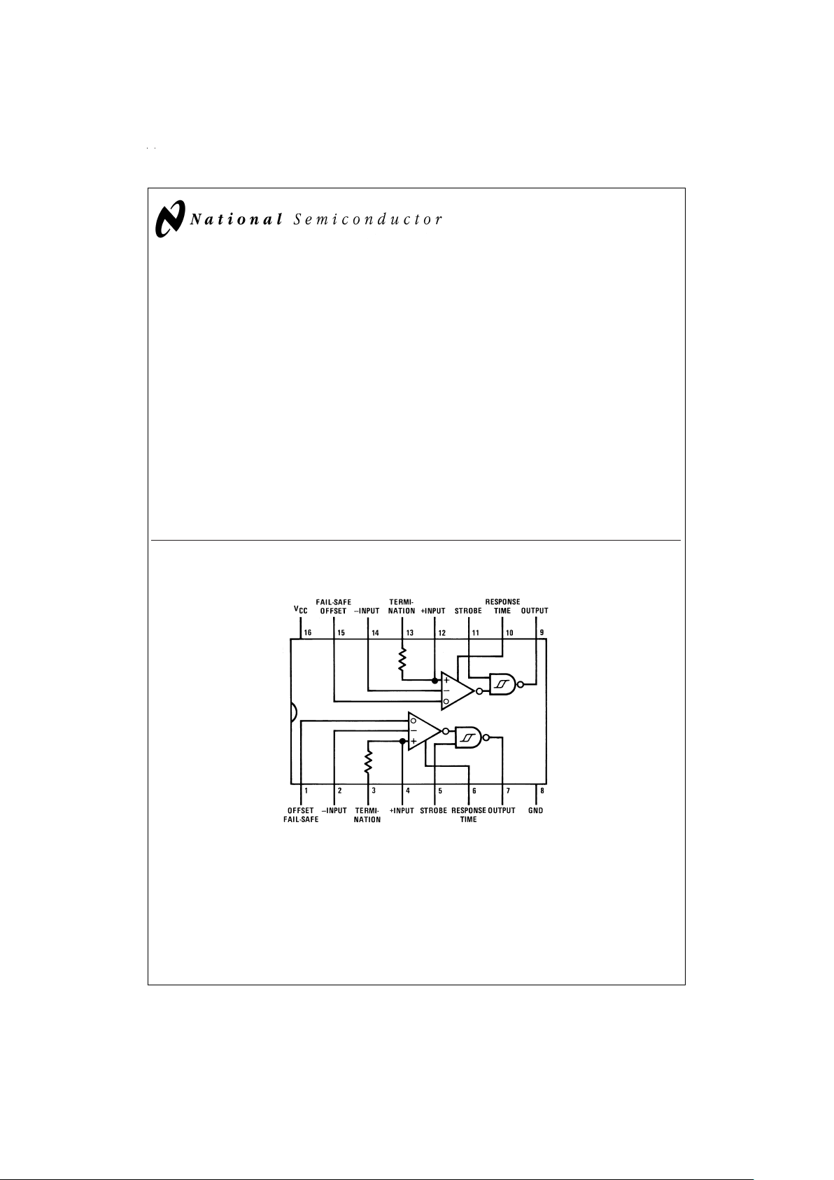
Connection Diagram
TRI-STATE®is a registered trademark of National Semiconductor Corporation.
Dual-In-Line Package
DS005801-1
Top View
For Complete Military Product Specifications,
refer to the appropriate SMD or MDS.
Order Number DS78C120J/883
See NS Package Number J16A
May 1999
DS78C120 Dual CMOS Compatible Differential Line Receiver
© 1999 National Semiconductor Corporation DS005801 www.national.com
Page 2
Absolute Maximum Ratings (Note 2)
If Military/Aerospace specified devices are required,
please contact the National Semiconductor Sales Office/
Distributors for availability and specifications.
Supply Voltage 18V
Input Voltage
±
25V
Strobe Voltage 18V
Output Sink Current 50 mA
Maximum Power Dissipation (Note 1) at 25˚C
Cavity Package 1433 mW
Molded Package 1362 mW
Storage Temperature Range −65˚C to +150˚C
Lead Temperature (Soldering, 4 seconds) 260˚C
Operating Conditions
Min Max Units
Supply Voltage (V
CC
) 4.5 15 V
Temperature (T
A
)
DS78C120 −55 +125 ˚C
Common-Mode Voltage (V
CM
) −15 +15 V
Note 1: Derate cavity package 9.6 mW/˚C; derate molded package
10.9 mW/˚C above 25˚C.
Electrical Characteristics (Notes 3, 4)
Symbol Parameter Conditions Min Typ Max Units
V
TH
Differential Threshold I
OUT
=
−200 µA, −7V ≤ V
CM
≤ 7V 0.06 0.2 V
Voltage V
OUT
≥ VCC− 1.2V −15V ≤ VCM≤ 15V 0.06 0.3 V
V
TL
Differential Threshold I
OUT
=
1.6 mA,V
OUT
≤ 0.5V −7V ≤ VCM≤ 7V −0.08 −0.2 V
Voltage −15V ≤ V
CM
≤ 15V −0.08 −0.3 V
V
TH
Differential Threshold I
OUT
=
−200 µA, −7V ≤ V
CM
≤ 7V 0.47 0.7 V
Voltage Fail-Safe V
OUT
≥ VCC− 1.2V
V
TL
Offset=5V I
OUT
=
1.6 mA,V
OUT
≤ 0.5V −7V ≤ VCM≤ 7V 0.2 0.42 V
R
IN
Input Resistance −15V ≤VCM≤ 15V, 0V ≤ VCC≤ 15V 4 5 kΩ
R
T
Line Termination
Resistance
T
A
=
25˚C 100 180 300 Ω
R
O
Offset Control Resistance T
A
=
25˚C 56 kΩ
I
IND
Data Input Current 0V ≤ VCC≤ 15V V
CM
=
10V 2 3.1 mA
(Unterminated) V
CM
=
0V 0 −0.5 mA
V
CM
=
−10V −2 −3.1 mA
V
THB
Input Balance I
OUT
=
200 µA, V
OUT
≥ −7V ≤ VCM≤ 7V 0.1 0.4 V
(Note 6) V
CC
− 1.2V, R
S
=
500Ω
I
OUT
=
1.6 mA,V
OUT
≤ 0.5V −7V ≤ VCM≤ 7V −0.1 −0.4 V
R
S
=
500Ω
V
OH
Logical “1” Output Voltage I
OUT
=
−200 µA, V
DIFF
=
1V V
CC
− 1.2 VCC− 0.75 V
V
OL
Logical “0” Output Voltage I
OUT
=
1.6 mA, V
DIFF
=
−1V 0.25 0.5 V
I
CC
Power Supply Current 15V ≤ VCM≤ −15V, V
CC
=
5.5V 8 15 mA
V
DIFF
=
−0.5V
(Both Receivers)
V
CC
=
15V 15 30 mA
I
IN(1)
Logical “1” Strobe Input
Current
V
STROBE
=
15V, V
DIFF
=
3V
15 100 µA
I
IN(0)
Logical “0” Strobe Input
Current
V
STROBE
=
0V, V
DIFF
=
−3V
−0.5 −100 µA
V
IH
Logical “1” Strobe Input VOL≤ 0.5V, I
OUT
=
1.6 mA V
CC
=
5V 3.5 2.5 V
Voltage V
CC
=
10V 8.0 5.0 V
V
CC
=
15V 12.5 7.5 V
V
IL
Logical “0” Strobe Input
Voltage
VOHVCC− 1.2V, V
CC
=
5V 2.5 1.5 V
I
OUT
=
−200 µA V
CC
=
10V 5.0 2.0 V
V
CC
=
15V 7.5 2.5 V
I
OS
Output Short-Circuit
Current
V
OUT
=
0V, V
CC
=
15V, V
STROBE
=
0V, (Note 5) −5 −20 −40 mA
Note 2: “Absolute Maximum Ratings” are those values beyond which the safety of the device cannot be guaranteed. Except for “Operating TemperatureRange”they
are not meant to imply that the devices should be operated at these limits. The table of “Electrical Characteristics” provides conditions for actual device operation.
Note 3: Unless otherwise specified min/max limits apply across the −55˚C to +125˚C temperature range for the DS78C120. All typical values for T
A
=
25˚C, V
CC
=
5V and V
CM
=
0V.
www.national.com 2
Page 3
Electrical Characteristics (Notes 3, 4) (Continued)
Note 4: All currents into device pins shown as positive, out of device pins as negative, all voltages referenced to ground unless otherwise noted. All values shown
as max or min on absolute value basis.
Note 5: Only one output at a time should be shorted.
Note 6: Refer to EIA-RS422 for exact conditions.
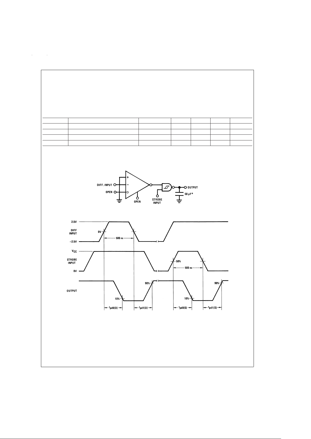
Switching Characteristics
V
CC
=
5V, T
A
=
25˚C
Symbol Parameter Conditions Min Typ Max Units
t
pd0(D)
Differential Input to “0” Output C
L
=
50 pF 60 100 ns
t
pd1(D)
Differential Input to “1” Output C
L
=
50 pF 100 150 ns
t
pd0(S)
Strobe Input to “0” Output C
L
=
50 pF 30 70 ns
t
pd1(S)
Strobe Input to “1” Output C
L
=
50 pF 100 150 ns
AC Test Circuit and Switching Time Waveforms
Differential and Strobe Input Signal
DS005801-3
*Includes probe and test fixture capacitance
DS005801-4
t
r
=
t
f
≤ 10 ns
PRR=1 MHz
Note: Optimum switching response is obtained by minimizing stray capacitance on Response Control pin (no external connection).
www.national.com3
Page 4

Schematic Diagram (
1
⁄2Circuit Shown)
DS005801-2
www.national.com 4
Page 5

Application Hints
The DS78C120 may be used a level transistor to interface between±12V MOS, ECL, TTL and CMOS. Toconfigure, bias either
input to voltage equal to
1
⁄2the voltage of the input signal, and the other input to the driving gate.
Balanced Data Transmission
DS005801-5
Unbalanced Data Transmission
DS005801-6
Logic Level Translator
DS005801-7
DS005801-8
www.national.com5
Page 6

Application Hints (Continued)
LINE DRIVERS
Line drivers which will interface with the DS78C120 are
listed below.
Balanced Drivers
DS26LS31Quad RS-422 Line Driver
DS7830, DS8830Dual TTL
DS7831, DS8831Dual TRI-STATE
®
TTL
DS7832, DS8832Dual TRI-STATE TTL
DS1691A, DS3691- Dual RS-422
DS1692, DS3692 Dual TRI-STATE
RS-422
DS3587, DS3487Quad TRI-STATE RS-422
Unbalanced Drivers
DS1488Quad RS-232
DS14C88Quad RS-232
DS75150Dual RS-232
RESPONSE CONTROL AND HYSTERESIS
In unbalanced (RS-232/RS-423) applications it is recommended that the rise time and fall time of the line driver be
controlled to reduce cross-talk. Elimination of switching
noise is accomplished in the DS78C120 by the 50 mV of
hysteresis incorporated in the output gate. This eliminates
the oscillations which may appear in a line receiver due to
the input signal slowly varying about the threshold level for
extended periods of time.
High frequency noise which is superimposed on the input
signal which may exceed 50 mV can be reduced in amplitude by filtering the device input. On the DS78C120, a high
impedance response control pin in the input amplifier is
available to filter the input signal without affecting the termination impedance of the transmission line. Noise pulse width
rejection vs the value of the response control capacitor is
shown in
Figure 1
and
Figure 2
. This combination of filters
followed by hysteresis will optimize performance in a worse
case noise environment.
TRANSMISSION LINE TERMINATION
On a transmission line which is electrically long, it is advisable to terminate the line in its characteristic impedance to
prevent signal reflection and its associated noise/cross-talk.
A180Ω termination resistor is provided in the DS78C120 line
receiver. To use the termination resistor, connect pins 2 and
3 together and pins 13 and 14 together. The 180Ω resistor
provides a good compromise between line reflections, power
dissipation in the driver, and IR drop in the transmission line.
If power dissipation and IR drop are still a concern, a capacitor may be connected in series with the resistor to minimize
power loss.
The value of the capacitor is recommended to be the line
length (time) divided by 3 times the resistor value. Example:
if the transmission line is 1,000 feet long, (approximately
1000 ns) the capacitor value should be 1852 pF. For additional application details, refer to application notes AN-22
and AN-108.
FAIL-SAFE OPERATION
Communication systems require elements of a system to detect the presence of signals in the transmission lines, and it
is desirable to have the system shut-down in a fail-safe
mode if the transmission line is open or shorted. To facilitate
the detection of input opens or shorts, the DS78C120 incorporates an input threshold voltage offset. This feature will
force the line receiver to a specific logic state if presence of
either fault is a condition.
Given that the receiver input threshold is
±
200 mV, an input
signal greater than
±
200 mV insures the receiver will be in a
specific logic state. When the offset control input (pins 1 and
15) is connected to V
CC
=
5V,the input thresholds are offset
from 200 mV to 700 mV, referred to the non-inverting input,
or −200 mV to −700 mV, referred to the inverting input.
Therefore, if the input is open or shorted, the input will be
greater than the input threshold and the receiver will remain
in a specified logic state.
DS005801-9
FIGURE 1. Noise Pulse Width vs
Response Control Capacitor
DS005801-10
DS005801-11
FIGURE 2.
www.national.com 6
Page 7

Application Hints (Continued)
The input circuit of the receiver consists of a 5k resistor terminated to ground through 120Ω on both inputs. This network acts as an attenuator, and permits operation with
common-mode input voltages greater than
±
15V.The offset
control input is actually another input to the attenuator,but its
resistor value is 56k. The offset control input is connected to
the inverting input side of the attenuator, and the input voltage to the amplifier is the sum of the inverting input plus 0.09
times the voltage on the offset control input. When the offset
control input is connected to 5V the input amplifier will see
V
IN(INVERTING)
+ 0.45V or V
IN(INVERTING)
+ 0.9V when the
control input is connected to 10V.The offset control input will
not significantly affect the differential performance of the receiver over its common-mode operating range, and will not
change the input impedance balance of the receiver.
It is recommended that the receiver be terminated (500Ω or
less) to insure it will detect an open circuit in the presence of
noise.
The offset control can be used to insure fail-safe operation
for unbalanced interface (RS-423) or for balanced interface
(RS-422) operation.
For unbalanced operation, the receiver would be in an indeterminate logic state if the offset control input was open.
Connecting the offset to 5V offsets the receiver threshold
0.45V.The output is forced to a logic zero state if the input is
open or shorted.
For balanced operation with inputs shorted or open, receiver
C will be in an indeterminate logic state. Receivers A and B
will be in a logic zero state allowing the NOR gate to detect
the short or open condition. The strobe will disable receivers
A and B and may therefore be used to sample the fail-safe
detector.Another method of fail-safe detection consists of filtering the output of the NOR gate D so it would not indicate
a fault condition when receiver inputs pass through the
threshold region, generating an output transient.
In a communications system, only the control signals are required to detect input fault condition. Advantages of a balanced data transmission system over an unbalanced transmission system are:
1. High noise immunity
2. High data ratio
3. Long line lengths
Unbalanced RS-423 and RS-232 Fail-Safe
DS005801-12
www.national.com7
Page 8

Application Hints (Continued)
Truth Table
(For Balanced Fail-Safe)
Input Strobe A-OUT B-OUT C-OUT D-OUT
0 1 0100
1 1 1010
X 1 00X1
0 0 1100
1 0 1100
X 0 1100
Balanced RS-422 Fail Safe
DS005801-13
DS005801-14 DS005801-15
DS005801-16
www.national.com 8
Page 9

Physical Dimensions inches (millimeters) unless otherwise noted
LIFE SUPPORT POLICY
NATIONAL’S PRODUCTS ARE NOT AUTHORIZED FOR USE AS CRITICAL COMPONENTS IN LIFE SUPPORT
DEVICES OR SYSTEMS WITHOUT THE EXPRESS WRITTEN APPROVAL OF THE PRESIDENT AND GENERAL
COUNSEL OF NATIONAL SEMICONDUCTOR CORPORATION. As used herein:
1. Life support devices or systems are devices or
systems which, (a) are intended for surgical implant
into the body, or (b) support or sustain life, and
whose failure to perform when properly used in
accordance with instructions for use provided in the
labeling, can be reasonably expected to result in a
significant injury to the user.
2. A critical component is any component of a life
support device or system whose failure to perform
can be reasonably expected to cause the failure of
the life support device or system, or to affect its
safety or effectiveness.
National Semiconductor
Corporation
Americas
Tel: 1-800-272-9959
Fax: 1-800-737-7018
Email: support@nsc.com
National Semiconductor
Europe
Fax: +49 (0) 1 80-530 85 86
Email: europe.support@nsc.com
Deutsch Tel: +49 (0) 1 80-530 85 85
English Tel: +49 (0) 1 80-532 78 32
Français Tel: +49 (0) 1 80-532 93 58
Italiano Tel: +49 (0) 1 80-534 16 80
National Semiconductor
Asia Pacific Customer
Response Group
Tel: 65-2544466
Fax: 65-2504466
Email: sea.support@nsc.com
National Semiconductor
Japan Ltd.
Tel: 81-3-5639-7560
Fax: 81-3-5639-7507
www.national.com
Ceramic Dual-In-Line Package (J)
Order Number DS78C120J/883
NS Package Number J16A
DS78C120 Dual CMOS Compatible Differential Line Receiver
National does not assume any responsibility for use of any circuitry described, no circuit patent licenses are implied and National reserves the right at any time without notice to change said circuitry and specifications.
 Loading...