

Page 1
TL/F/7560
DS75365 Quad TTL-to-MOS Driver
June 1992
DS75365 Quad TTL-to-MOS Driver
General Description
The DS75365 is a quad monolithic integrated TTL-to-MOS
driver and interface circuit that accepts standard TTL input
signals and provides high-current and high-voltage output
levels suitable for driving MOS circuits. It is used to drive
address, control, and timing inputs for several types of MOS
RAMs including the 1103.
The DS75365 operates from the TTL 5V supply and the
MOS V
SS
and VBBsupplies in many applications. This de-
vice has been optimized for operation with V
CC2
supply volt-
age from 16V to 20V, and with nominal V
CC3
supply voltage
from 3V to 4V higher than V
CC2
. However, it is designed so
as to be usable over a much wider range of V
CC2
and V
CC3
.
In some applications the V
CC3
power supply can be elimi-
nated by connecting the V
CC3
to the V
CC2
pin.
Features
Y
Quad positive-logic NAND TTL-to-MOS driver
Y
Versatile interface circuit for use between TTL and
high-current, high-voltage systems
Y
Capable of driving high-capacitance loads
Y
Compatible with many popular MOS RAMs
Y
Interchangeable with Intel 3207
Y
V
CC2
supply voltage variable over side range to 24V
maximum
Y
V
CC3
supply voltage pin available
Y
V
CC3
pin can be connected to V
CC2
pin in some
applications
Y
TTL compatible diode-clamped inputs
Y
Operates from standard bipolar and MOS supply
voltages
Y
Two common enable inputs per gate-pair
Y
High-speed switching
Y
Transient overdrive minimizes power dissipation
Y
Low standby power dissipation
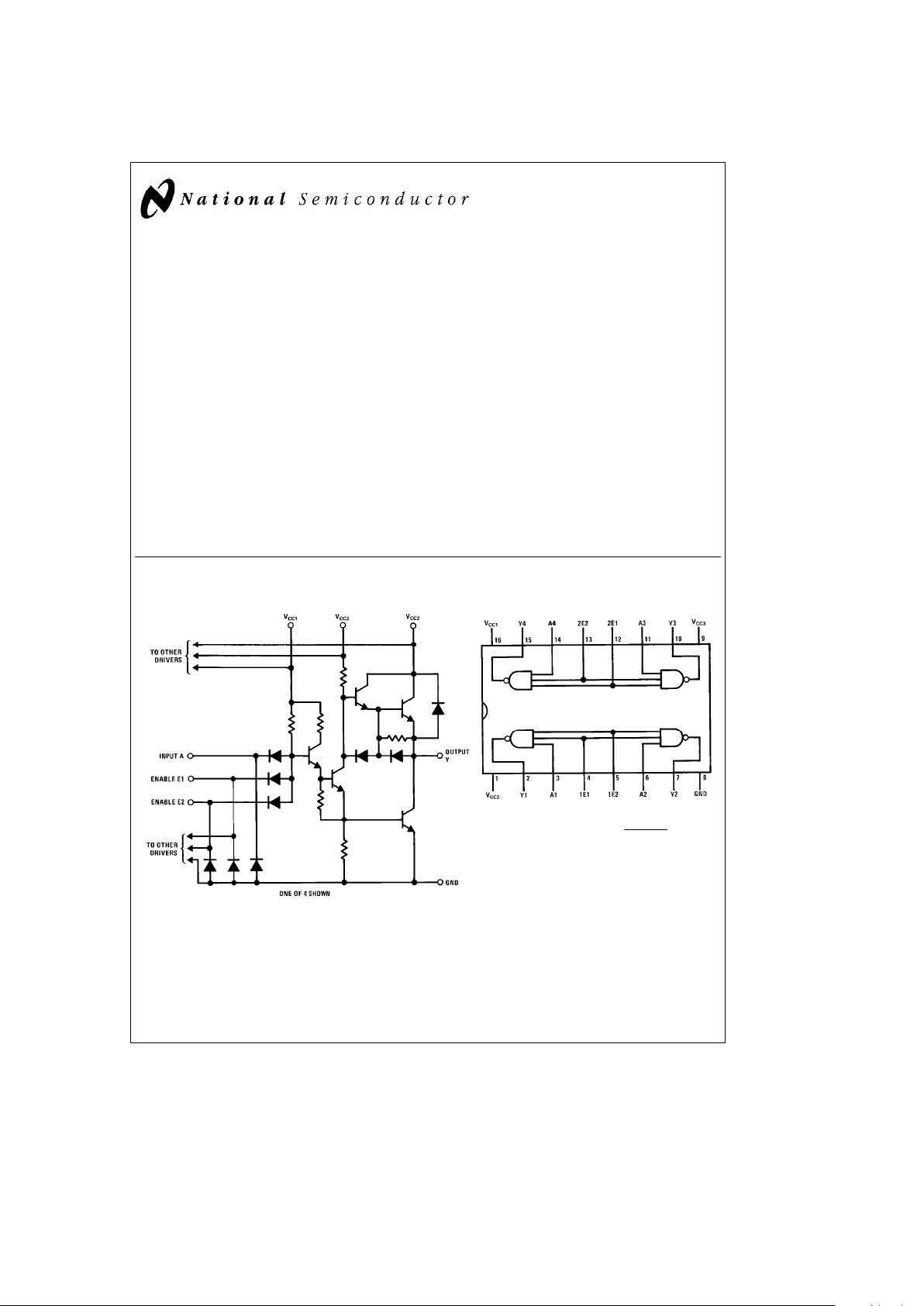
Schematic and Connection Diagrams
TL/F/7560– 1
Dual-In-Line Package
TL/F/7560– 2
Top View
Positive Logic: Y
e
A#E1#E2
Order Number DS75365N or DS75365WM
See NS Package Number M16B or N16A
C
1995 National Semiconductor Corporation RRD-B30M105/Printed in U. S. A.
Page 2
Absolute Maximum Ratings (Note 1)
If Military/Aerospace specified devices are required,
please contact the National Semiconductor Sales
Office/Distributors for availability and specifications.
Supply Voltage Range of V
CC1
b
0.5V to 7V
Supply Voltage Range of V
CC2
b
0.5V to 25V
Supply Voltage Range of V
CC3
b
0.5V to 30V
nput Voltage 5.5V
Inter-Input Voltage (Note 4) 5.5V
Storage Temperature Range
b
65§Ctoa150§C
Maximum Power Dissipation* at 25
§
C
Cavity Package 1509 mW
Molded Package 1476 mW
SO Package 1488 mW
Lead Temperature (Soldering, 10 sec) 300
§
C
* Derate cavity package 10.1 mW/§C above 25§C; derate molded package
11.8 mW/
§
C above 25§C, derate SO package 11.9 mW/§C above 25§C.
Operating Conditions
Min Max Units
Supply Voltage (V
CC1
) 4.75 5.25 V
Supply Voltage (V
CC2
) 4.75 24 V
Supply Voltage (V
CC3
)V
CC2
28 V
Voltage Difference Between 0 10 V
Supply Voltages: V
CC3–VCC2
Operating Ambient Temperature 0 70§C
Range (T
A
)
Electrical Characteristics (Notes 2 and 3)
Symbol Parameter Conditions Min Typ Max Units
V
IH
High-Level Input Voltage 2 V
V
IL
Low-Level Input Voltage 0.8 V
V
I
Input Clamp Voltage I
I
eb
12 mA
b
1.5 V
V
OH
High-Level Output Voltage V
CC3
e
V
CC2
a
3V, V
IL
e
0.8V, I
OH
eb
100 mAV
CC2
b
0.3 V
CC2
b
0.1 V
V
CC3
e
V
CC2
a
3V, V
IL
e
0.8V, I
OH
eb
10 mA V
CC2
b
1.2 V
CC2
b
0.9 V
V
CC3
e
V
CC2,VIL
e
0.8V, I
OH
eb
50 mAV
CC2
b
1V
CC2
b
0.7 V
V
CC3
e
V
CC2,VIL
e
0.8V, I
OH
eb
10 mA V
CC2
b
2.3 V
CC2
b
1.8 V
V
OL
Low-Level Output Voltage V
IH
e
2V, I
OL
e
10 mA 0.15 0.3 V
V
CC3
e
15V to 28V, V
IH
e
2V, I
OL
e
40 mA 0.25 0.5 V
V
O
Output Clamp Voltage V
I
e
0V, I
OH
e
20 mA V
CC2
a
1.5 V
I
I
Input Current at Maximum V
I
e
5.5V
1mA
Input Voltage
I
IH
High-Level Input Current V
I
e
2.4V A Inputs 40 mA
E1 and E2 Inputs 80 mA
I
IL
Low-Level Input Current V
I
e
0.4V A Inputs
b
1
b
1.6 mA
E1 and E2 Inputs
b
2
b
3.2 mA
I
CC1(H)
Supply Current from V
CC1,VCC1
e
5.25V, V
CC2
e
24V
48mA
All Outputs High V
CC3
e
28V, All Inputs at 0V, No Load
I
CC2(H)
Supply Current from V
CC2
,
b
2.2
a
0.25 mA
All Outputs High
b
2.2
b
3.2 mA
I
CC3(H)
Supply Current from V
CC3
,
2.2 3.5 mA
All Outputs High
I
CC1(L)
Supply Current from V
CC1,VCC1
e
5.25V, V
CC2
e
24V
31 47 mA
All Outputs Low V
CC3
e
28V, All Inputs at 5V, No Load
I
CC2(L)
Supply Current from V
CC2
,
3mA
All Outputs Low
I
CC3(L)
Supply Current from V
CC3
,
16 25 mA
All Outputs Low
I
CC2(H)
Supply Current from V
CC2,VCC1
e
5.25V, V
CC2
e
24V
0.25 mA
All Outputs High V
CC3
e
24V, All Inputs at 0V, No Load
I
CC3(H)
Supply Current from V
CC3
,
0.5 mA
All Outputs High
2
Page 3
Electrical Characteristics (Notes 2, 3) (Continued)
Symbol Parameter Conditions Min Typ Max Units
I
CC2(S)
Supply Current from V
CC2
,V
CC1
e
0V, V
CC2
e
24V
0.25 mA
Stand-By Condition V
CC3
e
24V, All Inputs at 5V, No Load
I
CC3(S)
Supply Current from V
CC3
,
0.5 mA
Stand-By Condition
Note 1: ‘‘Absolute Maximum Ratings’’ are those values beyond which the safety of the device cannot be guaranteed. Except for ‘‘Operating Temperature Range’’
they are not meant to imply that the devices should be operated at these limits. The table of ‘‘Electrical Characteristics’’ provides conditions for actual device
operation.
Note 2: Unless otherwise specified, min/max limits apply across the 0
§
Ctoa70§C range for the DS75365. All typical values are for T
A
e
25§C and V
CC1
e
5V and
V
CC2
e
20V and V
CC3
e
24V.
Note 3: All currents into device pins shown as positive, out of device pins as negative, all voltages referenced to ground unless otherwise noted. All values shown
as max or min on absolute value basis.
Note 4: This rating applies between any two inputs of any one of the gates.
Switching Characteristics V
CC1
e
5V, V
CC2
e
20V, V
CC3
e
24V, T
A
e
25§C
Symbol Parameter Conditions Min Typ Max Units
t
DLH
Delay Time, Low-to-High Level Output C
L
e
200 pF 11 20 ns
t
DHL
Delay Time, High-to-Low Level Output
R
D
e
24X
10 18 ns
t
TLH
Transition Time, Low-to-High Level Output
(
Figure 1
)
20 33 ns
t
THL
Transition Time, High-to-Low Level Output 20 33 ns
t
PLH
Propagation Delay Time, Low-to-High Level Output 10 31 48 ns
t
PHL
Propagation Delay Time, High-to-Low Level Output 10 30 46 ns
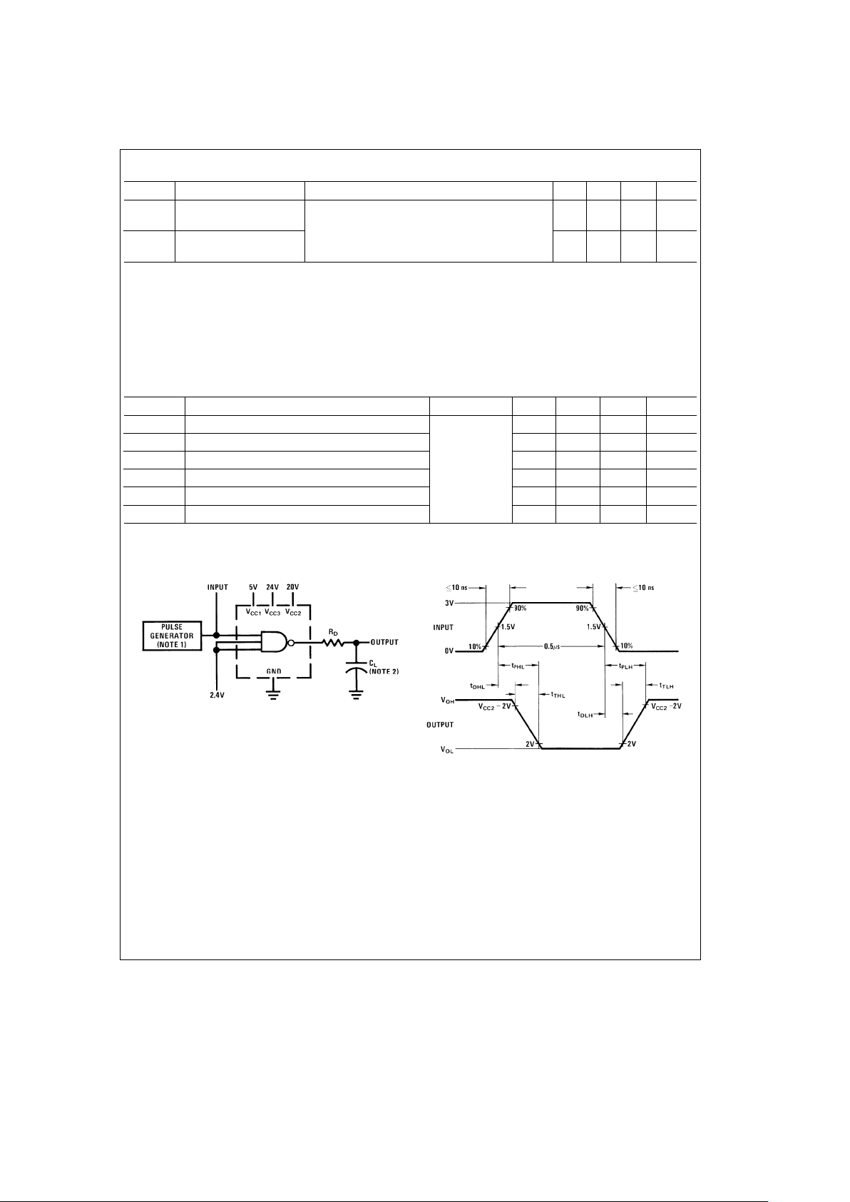
AC Test Circuit and Switching Time Waveforms
TL/F/7560– 3
TL/F/7560– 4
Note 1: The pulse generator has the following characteristics: PRRe1 MHz, Z
OUT
e
58X.
Note 2: C
L
includes probe and jig capacitance.
FIGURE 1. Switching Times, Each Driver
3
Page 4

Typical Performance Characteristics
Output Current
High-Level Output Voltage vs
Output Current
High-Level Output Voltage vs
Output Current
Low-Level Output Voltage
TL/F/7560– 5
Characteristics
Voltage Transfer
Drivers) vs Frequency
Total Dissipation (All Four
vs Ambient Temperature
Low-to-High Level Output
Propagation Delay Time,
High-to-Low Level Output
vs Ambient Temperature
Propagation Delay Time,
V
CC2
Supply Voltage
Low-to-High Level Output vs
Propagation Delay Time,
vs V
CC2
Supply Voltage
High-to-Low Level Output
Propagation Delay Time,
Load Capacitance
Low-to-High Level Output vs
Propagation Delay Time,
Load Capacitance
High-to-Low Level Output vs
Propagation Delay Time,
TL/F/7560– 6
4
Page 5

TL/F/7560– 7
FIGURE 2. Interconnection of DS75365 Devices
with 1103-Type Silicon-Gate MOS RAM
Typical Applications
The fast switching speeds of this device may produce undesirable output transient overshoot because of load or wiring
inductance. A small series damping resistor may be used to
reduce or eliminate this output transient overshoot. The optimum value of the damping resistor depends on the specific
load characteristics and switching speed. A typical value
would be between 10X and 30X (
Figure 3
).
Note: R
D
j
10X to 30X (Optional)
TL/F/7560– 8
FIGURE 3. Use of Damping Resistor to Reduce or
Eliminate Output Transient Overshoot in Certain
DS75365 Applications
Thermal Information
POWER DISSIPATION PRECAUTIONS
Significant power may be dissipated in the DS75365 driver
when charging and discharging high-capacitance loads over
a wide voltage range at high frequencies. The total dissipation curve shows the power dissipated in a typical DS75365
as a function of load capacitance and frequency. Average
power dissipation by this driver can be broken into three
components:
P
T(AV)
e
P
DC(AV)
a
P
C(AV)
a
P
S(AV)
where P
DC(AV)
is the steady-state power dissipation with the
output high or low, P
C(AV)
is the power level during charging
or discharging of the load capacitance, and P
S(AV)
is the
power dissipation during switching between the low and
high levels. None of these include energy transferred to the
load and all are averaged over a full cycle.
The power components per driver channel are:
P
DC(AV)
e
PLt
L
a
PHt
H
T
P
C(AV)jCVC
2
f
P
S(AV)
e
PLHt
LH
a
PHLt
HL
T
where the times are as defined in
Figure 4
.
PL,PH,PLH, and PHLare the respective instantaneous levels of power dissipation and C is load capacitance.
The DS75365 is so designed that P
S
is a negligible portion
of P
T
in most applications. Except at very high frequencies,
t
L
a
t
H
n
t
LH
a
tHLso that P
S
can be neglected. The total
dissipation curve for no load demonstrates this point. The
power dissipation contributions from all four channels are
then added together to obtain total device power.
The following example illustrates this power calculation
technique. Assume all four channels are operating identically with C
e
100 pF, f
e
2 MHz, V
CC1
e
5V, V
CC2
e
20V,
V
CC3
e
24V and duty cyclee60% outputs high
(t
H
/Te0.6). Also, assume V
OH
e
20V, V
OL
e
0.1V, PSis
negligible, and that the current from V
CC2
is negligible when
the output is low.
On a per-channel basis using data sheet values:
P
DC(AV)
e
Ð
(5V)
#
4mA
4
J
a
(20V)
#
b
2.2 mA
4
J
a
(24V)
#
2.2 mA
4
J(
(0.6)
a
Ð
(5V)
#
31 mA
4
J
a
(20V)
#
0mA
4
J
a
(24V)
#
16 mA
4
J(
(0.4)
P
DC(AV)
e
58 mW per channel
P
C(AV)
j
(100 pF) (19.9V)
2
(2 MHz)
P
C(AV)
j
79 mW per channel.
For the total device dissipation of the four channels:
P
T(AV)
j
4 (58
a
79)
P
T(AV)
j
548 mW typical for total package.
TL/F/7560– 9
FIGURE 4. Output Voltage Waveform
5
Page 6

6
Page 7

Physical Dimensions inches (millimeter)
Molded Dual-In-Line Package (M)
Order Number DS75365WM
NS Package Number M16B
7
Page 8

DS75365 Quad TTL-to-MOS Driver
Physical Dimensions inches (millimeter) (Continued)
Molded Dual-In-Line Package (N)
Order Number DS75365N
NS Package Number N16A
LIFE SUPPORT POLICY
NATIONAL’S PRODUCTS ARE NOT AUTHORIZED FOR USE AS CRITICAL COMPONENTS IN LIFE SUPPORT
DEVICES OR SYSTEMS WITHOUT THE EXPRESS WRITTEN APPROVAL OF THE PRESIDENT OF NATIONAL
SEMICONDUCTOR CORPORATION. As used herein:
1. Life support devices or systems are devices or 2. A critical component is any component of a life
systems which, (a) are intended for surgical implant support device or system whose failure to perform can
into the body, or (b) support or sustain life, and whose be reasonably expected to cause the failure of the life
failure to perform, when properly used in accordance support device or system, or to affect its safety or
with instructions for use provided in the labeling, can effectiveness.
be reasonably expected to result in a significant injury
to the user.
National Semiconductor National Semiconductor National Semiconductor National Semiconductor
Corporation Europe Hong Kong Ltd. Japan Ltd.
1111 West Bardin Road Fax: (
a
49) 0-180-530 85 86 13th Floor, Straight Block, Tel: 81-043-299-2309
Arlington, TX 76017 Email: cnjwge@tevm2.nsc.com Ocean Centre, 5 Canton Rd. Fax: 81-043-299-2408
Tel: 1(800) 272-9959 Deutsch Tel: (
a
49) 0-180-530 85 85 Tsimshatsui, Kowloon
Fax: 1(800) 737-7018 English Tel: (
a
49) 0-180-532 78 32 Hong Kong
Fran3ais Tel: (
a
49) 0-180-532 93 58 Tel: (852) 2737-1600
Italiano Tel: (
a
49) 0-180-534 16 80 Fax: (852) 2736-9960
National does not assume any responsibility for use of any circuitry described, no circuit patent licenses are implied and National reserves the right at any time without notice to change said circuitry and specifications.
 Loading...