

Page 1

DS75160A/DS75161A
IEEE-488 GPIB Transceivers
DS75160A/DS75161A IEEE-488 GPIB Transceivers
May 1999
General Description
This family of high-speed-Schottky 8-channel bi-directional
transceivers is designed to interface TTL/MOS logic to the
IEEE Standard 488-1978 General Purpose Interface Bus
(GPIB). PNP inputs are usedatalldriver inputs for minimum
loading, and hysteresis is provided at all receiver inputs for
added noise margin. The IEEE-488 required bus termination
is provided internally with an active turn-off feature which disconnects the termination from the bus when V
The General Purpose Interface Bus is comprised of 16 signal lines — 8 for data and 8 for interface management. The
data lines are always implemented with DS75160A, and the
management lines are either implemented with DS75161A in
a single-controller system.
is removed.
CC
Connection Diagrams
Dual-In-Line Package
Features
n 8-channel bi-directional non-inverting transceivers
n Bi-directional control implemented with TRI-STATE
output design
n Meets IEEE Standard 488-1978
n High-speed Schottky design
n Low power consumption
n High impedance PNP inputs (drivers)
n 500 mV (typ) input hysteresis (receivers)
n On-chip bus terminators
n No bus loading when V
n Pin selectable open collector mode on DS75160A driver
outputs
n Accommodates multi-controller systems
Dual-In-Line Package
Order Number DS75161AN or DS75161AWM
See NS Package Number M20B or N20B
is removed
CC
®
DS005804-16
DS005804-1
Order Number DS75160AN or DS75160AWM
See NS Package Number M20B or N20A
TRI-STATE®is a registered trademark of National Semiconductor Corporation.
© 1999 National Semiconductor Corporation DS005804 www.national.com
Top View
Page 2
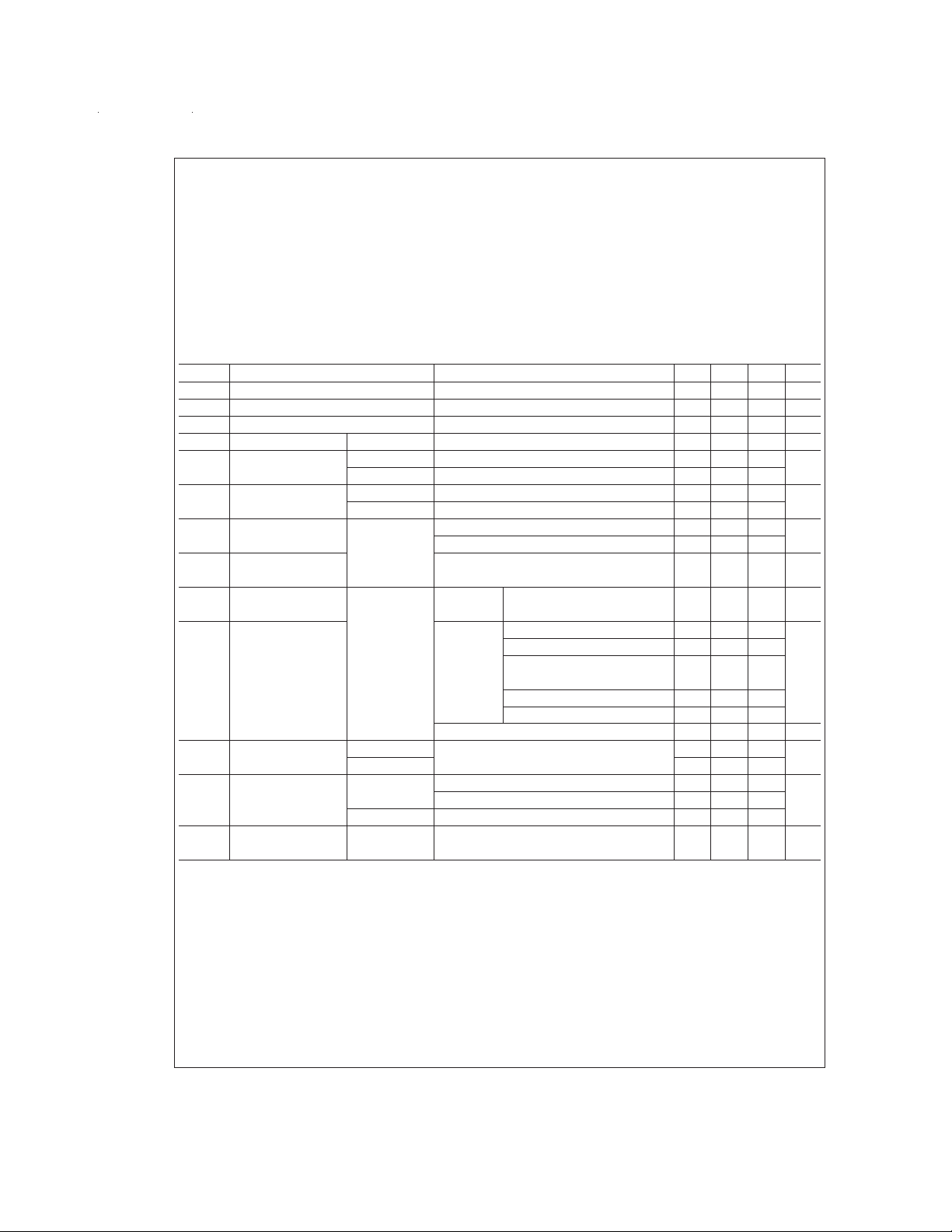
Absolute Maximum Ratings (Note 2)
If Military/Aerospace specified devices are required,
please contact the National Semiconductor Sales Office/
Distributors for availability and specifications.
Supply Voltage, V
CC
Input Voltage 5.5V
Storage Temperature Range −65˚C to +150˚C
Lead Temperature (Soldering, 4 sec.) 260˚C
7.0V
Molded Package 1897 mW
Min Max Units
, Supply Voltage 4.75 5.25 V
V
CC
, Ambient Temperature 0 70 ˚C
T
A
, Output Low Current
I
OL
Bus 48 mA
Terminal 16 mA
Note 1: Derate molded package 15.2 mW/˚C above 25˚C.
Maximum Power Dissipation (Note 1) at 25˚C
Electrical Characteristics (Notes 3, 4)
Symbol Parameter Conditions Min Typ Max Units
V
IH
V
IL
V
IK
V
HYS
V
OH
V
OL
I
IH
I
IL
V
BIAS
I
LOAD
I
OS
I
CC
C
IN
Note 2: “Absolute Maximum Ratings” are those values beyond which the safety of the device cannot be guaranteed. They are not meant to imply that the device
should be operated at these limits. The table of “Electrical Characteristics” provides conditions for actual device operation.
Note 3: Unless otherwise specified, min/max limits apply across the 0˚C to +70˚C temperature range and the 4.75V to 5.25V power supply range. All typical values
are for T
Note 4: All currents into device pins are shown as positive; all currents out of device pins are shown as negative; all voltages are referenced to ground, unless otherwise specified. All values shown as max or min are so classified on absolute value basis.
Note 5: Only one output at a time should be shorted.
Note 6: This characteristic does not apply to outputs on DS75161A that are open collector.
High-Level Input Voltage 2 V
Low-Level Input Voltage 0.8 V
Input Clamp Voltage I
=
−18 mA −0.8 −1.5 V
I
Input Hysteresis Bus 400 500 mV
High-Level Terminal I
Output Voltage Bus (Note 4) I
Low-Level Terminal I
Output Voltage Bus I
High-Level Terminal and V
Input Current TE, PE, DC, V
Low-Level SC Inputs V
=
−800 µA 2.7 3.5 V
OH
=
−5.2 mA 2.5 3.4
OH
=
16 mA 0.3 0.5 V
OL
=
48 mA 0.4 0.5
OH
=
5.5V 0.2 100 µA
I
=
2.7V 0.1 20
I
=
0.5V −10 −100 µA
I
Input Current
Terminator Bias Driver I
=
0 (No Load) 2.5 3.0 3.7 V
I(bus)
Voltage at Bus Port Disabled
Terminator V
Bus Loading V
Current Bus Driver V
=
−1.5V to 0.4V −1.3
I(bus)
=
0.4V to 2.5V 0 −3.2
I(bus)
=
2.5V to 3.7V 2.5 mA
I(bus)
Disabled −3.2
=
V
3.7V to 5V 0 2.5
I(bus)
=
V
5V to 5.5V 0.7 2.5
I(bus)
0V, V
=
0V to 2.5V 40 µA
I(bus)
=
0V (Note 5) −15 −35 −75 mA
O
Short-Circuit Terminal V
=
V
CC
=
2V, V
I
Output Current Bus (Note 6) −35 −75 −150
Supply Current DS75160A Transmit, TE=2V, PE=2V, V
Receive, TE=0.8V, PE=2V, V
DS75161A TE=0.8V, DC=0.8V, V
Bus-Port Bus V
=
CC
5V or 0V, V
=
0V to 2V, 20 30 pF
I
=
0.8V 85 125
I
=
0.8V 70 100 mA
I
=
0.8V 84 125
I
Capacitance f=1 MHz
=
A
25˚C and V
=
5.0V.
CC
www.national.com 2
Page 3
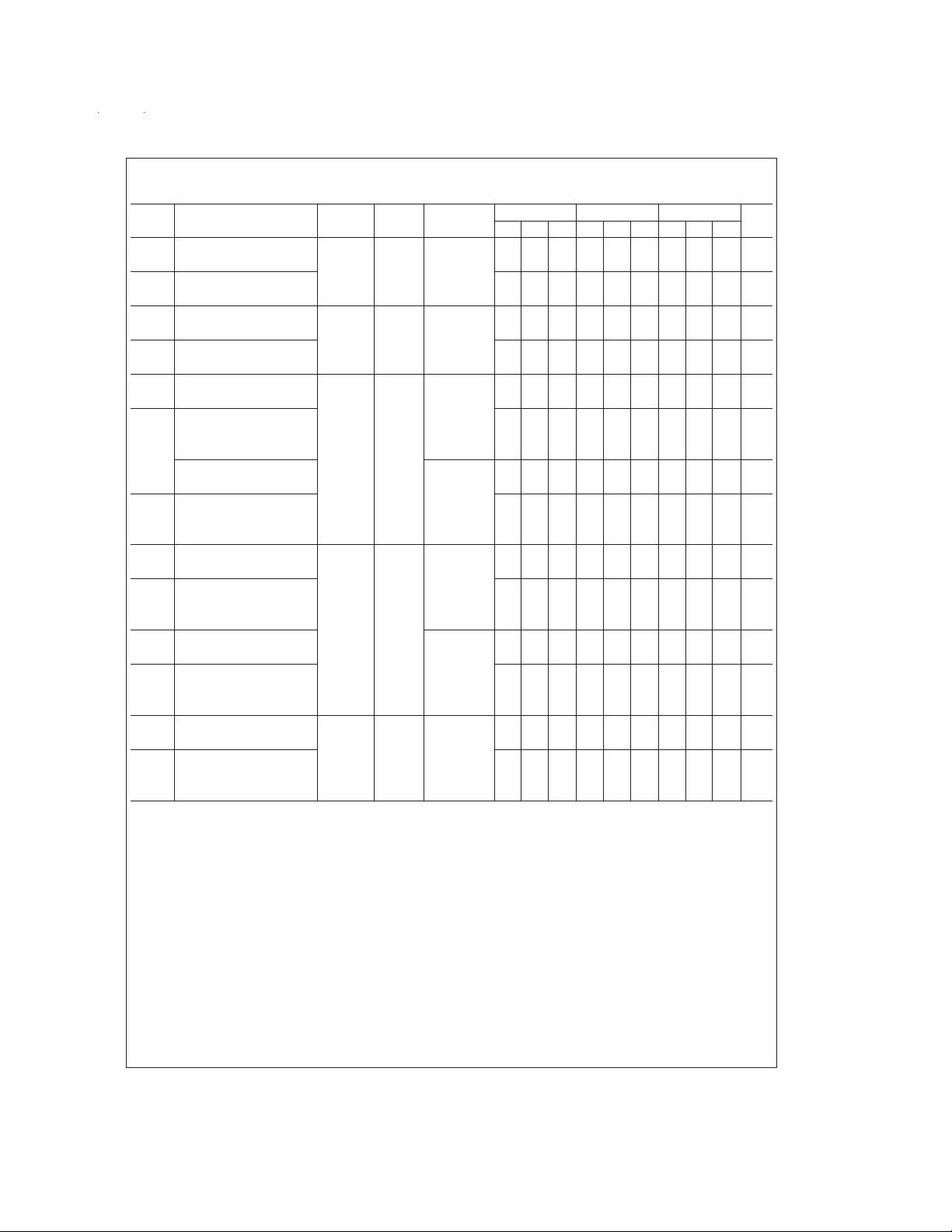
Switching Characteristics (Note 7)
=
V
5.0V
CC
Symbol Parameter From To Conditions DS75160A DS75161A DS75162A Units
Propagation Delay Time, V
t
PLH
Low to High Level Output Terminal Bus R
t
Propagation Delay Time, C
PHL
High to Low Level Output
t
Propagation Delay Time, V
PLH
Low to High Level Output Bus Terminal R
t
Propagation Delay Time, C
PHL
High to Low Level Output
t
Output Enable Time V
PZH
to High Level V
t
Output Disable Time TE, DC, R
PHZ
From High Level or SC C
t
Output Enable Time (Note 8) Bus V
PZL
to Low Level (Note 9) V
t
Output Disable Time R
PLZ
From Low Level C
t
Output Enable Time V
PZH
to High Level V
t
Output Disable Time TE, DC, R
PHZ
From High Level or SC Terminal C
t
Output Enable Time (Note 8) V
PZL
to Low Level (Note 9) V
t
Output Disable Time R
PLZ
From Low Level C
t
Output Pull-Up Enable V
PZH
Time (DS75160A Only) PE Bus V
t
Output Pull-Up Disable (Note 8) R
PHZ
Time (DS75160A Only) C
Note 7: Typical values are for V
Note 8: Refer to Functional Truth Tables for control input definition.
Note 9: Test configuration should be connected to only one transceiver at a time due to the high current stress caused by the V
nected to that input becomes active.
±
5%,T
=
0˚C to 70˚C
A
CC
=
5.0V and T
=
L
=
L
=
L
Figure 1
=
L
=
L
=
L
Figure 2
=
I
=
L
=
L
=
L
Figure 1
=
I
=
L
=
L
=
L
Figure 1
=
I
=
L
=
L
=
L
Figure 1
=
I
=
L
=
L
=
L
Figure 1
=
I
=
L
=
L
=
L
Figure 1
=
25˚C and are meant for reference only.
A
Min Typ Max Min Typ Max Min Typ Max
2.3V 10 20 10 20 10 20 ns
38.3Ω
30 pF 14 20 14 20 14 20 ns
5.0V 14 20 14 20 14 20 ns
240Ω
30 pF 10 20 10 20 10 20 ns
3.0V 19 32 23 40 23 40 ns
0V
480Ω 15 22 15 25 15 25 ns
15 pF
0V 24 35 28 48 28 48 ns
2.3V
38.3Ω 17 25 17 27 17 27 ns
15 pF
3.0V 17 33 18 40 18 40 ns
0V
3kΩ 15 25 22 33 22 33 ns
15 pF
0V 25 39 28 52 28 52 ns
5V
280Ω 15 27 20 35 20 35 ns
15 pF
3V 10 17 NA NA ns
0V
480Ω 10 15 NA NA ns
15 pF
voltage source when the output con-
I
www.national.com3
Page 4

Switching Load Configurations
VClogic high=3.0V
logic low=0V
V
C
includes jig and probe capacitance
*C
L
FIGURE 1.
Connection Diagrams
DS005804-8
VClogic high=3.0V
logic low=0V
V
C
includes jig and probe capacitance
*C
L
Dual-In-Line Package
DS005804-9
FIGURE 2.
Top View
Functional Description
DS75160A
This device is an 8-channel bi-directional transceiver with
one common direction control input, denoted TE. When used
to implement the IEEE-488 bus, this device is connected to
the eight data bus lines, designated DIO
connections to the bus lines have internal terminators, in accordance with the IEEE-488 Standard, that are deactivated
when the device is powered down. This feature guarantees
no bus loading when V
have a control mode that either enables or disables the ac-
=
0V. The bus port outputs also
CC
tive upper stage of the totem-pole configuration. When this
control input, denoted PE, is in the high state, the bus outputs operate in the high-speed totem-pole mode. When PE
is in the low state, the bus outputs operate as open collector
outputs which are necessary for parallel polling.
DS75161A
www.national.com 4
–DIO8. The port
1
DS005804-2
This device is also an 8-channel bi-directional transceiver
which is specifically configured to implement the eight management signal lines of the IEEE-488 bus. This device,
paired with the DS75160A, forms the complete 16-line interface between the IEEE-488 bus and a single controller instrumentation system. In compliance with the system organization of the management signal lines, the SRQ, NDAC, and
NRFD bus port outputs are open collector. In contrast to the
DS75160A, these open collector outputs are a fixed configuration. The direction control is divided into three groups. The
DAV, NDAC, and NRFD transceiver directions are controlled
by the TE input. The ATN, SRQ, REN, and IFC transceiver
directions are controlled by the DC input. The EOI transceiver direction is a function of both the TE and DC inputs, as
well as the logic level present on the ATN channel. The port
connections to the bus lines have internal terminators identical to the DS75160A.
Page 5

Functional Description (Continued)
Table of Signal Line Abbreviations
Signal Line Mne-
Classi- monic Definition Device
fication
DC Direction Control DS75161A
Control PE Pull-Up Enable DS75160A
Signals TE Talk Enable All
SC System Controller
Data B1–B8 Bus Side of Device
I/O Ports D1–D8 Terminal Side DS75160A
of Device
ATN Attention
DAV Data Valid
EOI End or Identify
Management IFC Interface Clear DS75161A
Signals NDAC Not Data Accepted
NRFD Not Ready for Data
REN Remote Enable
SRQ Service Request
Logic Diagrams
DS75160A
DS005804-4
www.national.com5
Page 6

Logic Diagrams (Continued)
DS75161A
Switching Waveforms
Transmit Propagation Delays
www.national.com 6
DS005804-5
DS005804-7
DS005804-10
Page 7

Switching Waveforms (Continued)
Terminal Enable/Disable Times
Receive Propagation Delays
DS005804-11
DS005804-12
Bus Enable/Disable Times
*Input signal: f=1.0 MHz, 50%duty cycle, t
=
≤ 5ns
t
r
f
Performance Characteristics
Refer to Electrical Characteristics table
DS005804-13
Bus Port Load Characteristics
DS005804-14
www.national.com7
Page 8

Functional Truth Tables
DS75160A
Control Input Data Transceivers
TE PE Direction Bus Port Configuration
H H T Totem-Pole Output
H L T Open Collector Output
L X R Input
DS75161A
Control Input Level Transceiver Signal Direction
TE DC ATN
HH R RRTRRT
HL T TTRRRT
LHRRRTTTR
LL T TTRTTR
HXH T
LXH R
XHL R
XLL T
=
H
High level input
L=Low level input
X=Don’t care
T=Transmit, i.e., signal outputted to bus
R=Receive, i.e., signal outputted to terminal
*
The ATN signal level is sensed for internal multiplex control of EOI transmission direction logic.
Level
*
EOI REN IFC SRQ NRFD NDAC DAV
www.national.com 8
Page 9

Physical Dimensions inches (millimeters) unless otherwise noted
Order Number DS75160AWM
NS Package Number M20B
www.national.com9
Page 10

Physical Dimensions inches (millimeters) unless otherwise noted (Continued)
Molded Dual-In-Line Package (N)
Order Number DS75160AN or DS75161AN
NS Package Number N20A
DS75160A/DS75161A IEEE-488 GPIB Transceivers
LIFE SUPPORT POLICY
NATIONAL’S PRODUCTS ARE NOT AUTHORIZED FOR USE AS CRITICAL COMPONENTS IN LIFE SUPPORT
DEVICES OR SYSTEMS WITHOUT THE EXPRESS WRITTEN APPROVAL OF THE PRESIDENT AND GENERAL
COUNSEL OF NATIONAL SEMICONDUCTOR CORPORATION. As used herein:
1. Life support devices or systems are devices or
systems which, (a) are intended for surgical implant
into the body, or (b) support or sustain life, and
whose failure to perform when properly used in
accordance with instructions for use provided in the
2. A critical component is any component of a life
support device or system whose failure to perform
can be reasonably expected to cause the failure of
the life support device or system, or to affect its
safety or effectiveness.
labeling, can be reasonably expected to result in a
significant injury to the user.
National Semiconductor
Corporation
Americas
Tel: 1-800-272-9959
Fax: 1-800-737-7018
Email: support@nsc.com
www.national.com
National does not assume any responsibility for use of any circuitry described, no circuit patent licenses are implied and National reserves the right at any time without notice to change said circuitry and specifications.
National Semiconductor
Europe
Fax: +49 (0) 1 80-530 85 86
Email: europe.support@nsc.com
Deutsch Tel: +49 (0) 1 80-530 85 85
English Tel: +49 (0) 1 80-532 78 32
Français Tel: +49 (0) 1 80-532 93 58
Italiano Tel: +49 (0) 1 80-534 16 80
National Semiconductor
Asia Pacific Customer
Response Group
Tel: 65-2544466
Fax: 65-2504466
Email: sea.support@nsc.com
National Semiconductor
Japan Ltd.
Tel: 81-3-5639-7560
Fax: 81-3-5639-7507
 Loading...