

Page 1

1 of 6 102299
FEATURES
§ Factory calibrated for sensitivity of +6.20
mV/°C and thermometer accuracy of ±2.0°C
over the 0°C to 85°C range and ±3°C over the
40°C to 0°C and +85°C to +125°C range
§ Measurement range of -40°C to +125°C
§ Integrated temperature sensor and voltage
reference
§ Two independent temperature setpoints with
respective logic outputs with set hysteresis
§ Narrow-body SO8 (150-mil) package
§ Wide power supply range (2.7V ≤ VDD ≤
5.5V)
§ Functionally compatible with LM56xIM
§ Applications include monitoring disk drives,
printers, office equipment, HVAC,
appliances, or any power/cost/temperaturesensitive environments.
PIN ASSIGNMENT
PIN DESCRIPTION
V
REF
- Bandgap Voltage Reference
Output
V
T2
- Temperature Trip Point 2
V
T1
- Temperature Trip Point 1
GND - Ground
V
TEMP
- Temp Sensor Output Voltage
T
OUT2
- Thermostat output for Trip
Point 2
T
OUT1
- Thermostat output for Trip
Point 1
V
DD
- Power Supply Voltage (2.7V
to 5.5V)
DESCRIPTION
The DS56 Dual Temperature Comparator has two independent open-drain thermostat outputs and
respective trip point inputs. The trip points are set with external resistors that divide down the 1.25V
internal bandgap voltage reference. The voltage resulting from this resistive division is compared with the
voltage corresponding to the device’s junction temperature to define the thermostat output logic state. The
internal temperature sensor has a typical sensitivity of +6.2mV/°C and DC offset of +395 mV at 0°C.
Both thermostat outputs have 5°C of hysteresis.
For applications that require temperature measurement as well as control, the temperature sensor voltage
is brought out to a pin.
The DS56 is packaged in a compact 150-mil, 8-pin SOIC. Applications include disk drives, printers,
office equipment, HVAC, appliances, or any power/cost/temperature-sensitive environments.
DS56
Dual Temperature Comparator
PRELIMINARY
www.dalsemi.com
1
2
3
4
8
7
6
5
V
DD
T
OUT1
T
OUT2
V
TEMP
V
REF
V
T2
V
T1
GND
DS56S 8-Pin SOIC (150-mil)
Page 2
DS56
2 of 6 102299
DETAILED PIN DESCRIPTION Table 1
PIN SYMBOL TYPE DESCRIPTION
1 V
REF
Analog output Bandgap output 1.25V (nom) voltage reference output.
2 V
T2
Analog input Trip point 2 input associated with thermostat output 2.
3 V
T1
Analog input Trip point 1 input associated with thermostat output 1.
4 GND GND
Ground pin.
5 V
TEMP
Analog output Temperature sensor output. (+6.2 T
DegC
+ 395) mV.
6 T
OUT2
Digital output
(open-drain)
Thermostat output 2. Active low output corresponding to trip
point 2. Typical hysteresis is 5.0°C.
7 T
OUT1
Digital output
(open-drain)
Thermostat output 1. Active low output corresponding to trip
point 1. Typical hysteresis is 5.0°C.
8 V
DD
V
DD
Supply Voltage 2.7V - 5.5V input power pin.
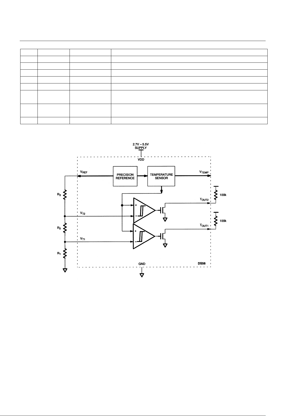
DS56 FUNCTIONAL BLOCK DIAGRAM Figure 1
Page 3
DS56
3 of 6 102299
OVERVIEW
A block diagram of the DS56 is shown in Figure 1. The DS56 consists of three major components:
1. Precision bandgap voltage reference
2. Temperature sensor
3. Thermostat comparators
The DS56 incorporates an internal temperature sensor with a typical transfer function of (in mV with T
expressed in °C):
V
TEMP
(T) = 6.2 T + 395
The voltage associated with this transfer function is output on the V
TEMP
pin, which has a typical output
impedance of 1.5 kΩ.
The DS56 has two independent temperature comparators, each with its own input (or trip point) and
output. The comparison voltage (the V
TEMP
transfer function) is the same for both comparators.
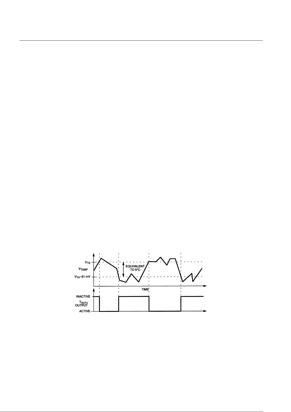
Additionally, the hysteresis for both comparators is typically 5°C (31.0 mV).
The DS56 bandgap voltage reference is available on pin 1 to allow for a designer to set the trip point(s)
by resistively dividing the reference voltage. One possible scenario is illustrated in Figure 1. For optimum
performance, the VREF pin should be connected to a 50 µA load.
The comparator outputs are taken off-chip via open-drain FETs, thus requiring external pullups. The
thermostat transfer function is illustrated in Figure 2.
The supply range of the DS56 is 2.7V to 5.5V, allowing for applications ranging from industrial control
to battery-powered portable equipment.
THERMOSTAT OUTPUT TRANSFER FUNCTION Figure 2
Page 4

DS56
4 of 6 102299
ABSOLUTE MAXIMUM RATINGS*
Voltage on V
DD
(GND-0.3V) to +7.0V
Input Current at any pin 5.0 mA
Package Input Current 20 mA
Operating Temperature -40°C to +125°C
Storage Temperature -55°C to 150°C
ESD Susceptibility (Human Body Model) 1kV
Soldering Temperature (Note 2) 215°C for 60 seconds (Vapor Phase)
220°C for 15 seconds (IR)
* This is a stress rating only and functional operation of the device at these or any other conditions
above those indicated in the operation sections of this specification is not implied. Exposure to
absolute maximum rating conditions for extended periods of time may affect reliability.
The Dallas Semiconductor DS56 is built to the highest quality standards and manufactured for long-term
reliability. All Dallas Semiconductor devices are made using the same quality materials and
manufacturing methods. However, the DS56 is not exposed to environmental stresses, such as burn-in,
that some industrial applications require. For specific reliability information on this product, please
contact the factory in Dallas at (972) 371-4448.
RECOMMENDED DC OPERATING CONDITIONS:
(-40°C to +125°C; 2.7V ≤ VDD ≤ 5.5V)
PARAMETER SYMBOL CONDITION MIN TYP MAX UNITS NOTES
Supply Voltage V
DD
2.7 5.5 V 1
DC ELECTRICAL CHARACTERISTICS:
Power Supply (Note 3) (-40°C to +125°C; 2.7V ≤ VDD ≤ 5.5V)
PARAMETER SYMBOL CONDITION MIN TYP MAX UNITS NOTES
Supply Current I
DD
225 µA
DC ELECTRICAL CHARACTERISTICS:
Temperature Sensor (Note 3) (-40°C to +125°C; 2.7V ≤ VDD ≤ 5.5V)
PARAMETER SYMBOL CONDITION MIN TYP MAX UNITS NOTES
-40°C≤TA≤125°C ±3
Trip Point
Accuracy
TP
ERR
0°C≤TA≤85°C
±2
°C 4
-40°C≤TA≤125°C ±3
V
TEMP
Accuracy T
ERR
0°C≤TA≤85°C
±2
°C 5
V
TEMP
DC Offset T=0°C 395 mV
Sensor Gain
?V/?T
6.25 mV/°C
Trip Point
Hysteresis
TP
HYST
3.0 5.0 7.0 °C
2.7V≤VDD≤3.3V
±2.3 mV
Power Supply
Regulation
3.0V≤VDD≤5.5V
±0.3 mV/V
V
TEMP
Output
Impedance
1500
Ω
Page 5

DS56
5 of 6 102299
DC ELECTRICAL CHARACTERISTICS:
Bandgap Voltage Reference V
REF
(-40°C to +125°C; 2.7V ≤ VDD ≤ 5.5V)
PARAMETER SYMBOL CONDITION MIN TYP MAX UNITS NOTES
V
REF
Output V
REF
1.238 1.25 1.263 V
2.7V≤VDD≤3.3V
±1.45 mV
Power Supply
Regulation
?V
REF
/
?V
DD
30V≤VDD≤5.5V
±0.2 mV/V
Load Regulation
?V
REF
/
?I
L
+3.0µA≤IL≤
+50µA
0.15 mV/µA
DC ELECTRICAL CHARACTERISTICS:
Trip Point Inputs VT1/V
T2
(-40°C to +125°C; 2.7V ≤ VDD ≤ 5.5V)
PARAMETER SYMBOL CONDITION MIN TYP MAX UNITS NOTES
Input Bias Current I
BIAS
300 nA
Input Range V
TIN
0
(V
DD
-1.0)
V
DC ELECTRICAL CHARACTERISTICS:
Thermostat Outputs T
OUT1/TOUT2
(-40°C to +125°C; 2.7V ≤ VDD ≤ 5.5V)
PARAMETER SYMBOL CONDITION MIN TYP MAX UNITS NOTES
Logic 1 Output
Leakage Current
I
OUT1
VDD = 5.0V 1.0 µA
LOGICAL 0
Output Voltage
V
OUT0
I
OUT
= +50 µA 0.4 V
NOTES:
1. All voltages are referenced to ground, unless otherwise specified.
2. Solder according to IPC standards.
3. Specified for V
TEMP
sourcing 1.0 µA (max) and V
REF
load current = 50 µA.
4. Includes error associated with internal temperature sensor, bandgap voltage V
REF
, and comparator
offset. External resistance tolerance and temperature coefficient not included in this spec.
5. Thermometer error (expressed in °C) is the difference between [VO(T) - 395]/6.20 and the DS56 case
temperature at VDD = 3.0V, thus taking into account sensor error, DC offset error, sensor amplifier
gain variations, and amplifier nonlinearity.
TYPICAL DS56 THERMOMETER ERROR Figure 3
TBD
TYPICAL DS56 V
TEMP
TRANSFER FUNCTION Figure 4
TBD
Page 6
DS56
6 of 6 102299
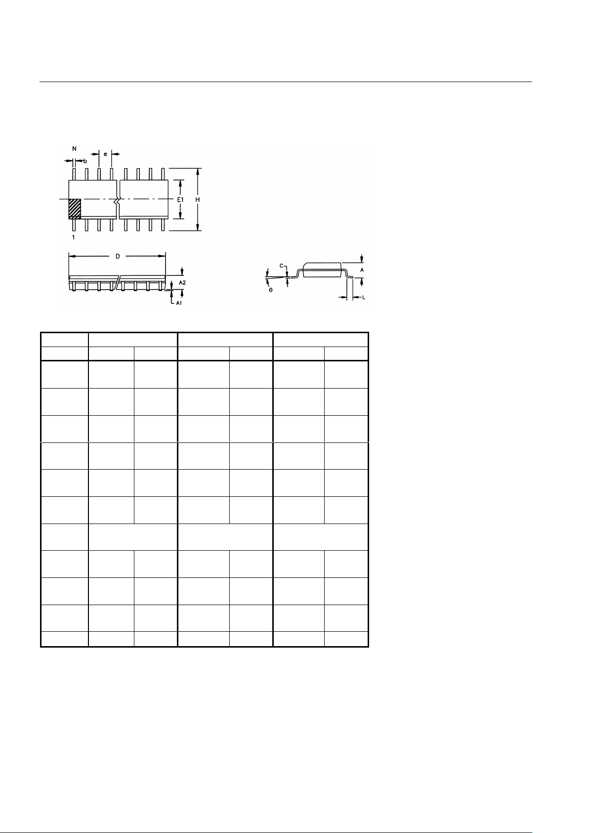
DS56 PHYSICAL DIMENSIONS
8-, 14-, AND 16-PIN SOIC (.150” BODY WIDTH)
PKG 8-PIN 14-PIN 16-PIN
DIM MIN MAX MIN MAX MIN MAX
A IN.
MM
0.053
1.35
0.069
1.75
0.053
1.35
0.069
1.75
0.053
1.35
0.069
1.75
A1 IN.
MM
0.004
0.10
0.010
0.25
0.004
0.10
0.010
0.25
0.004
0.10
0.010
0.25
A2 IN.
MM
0.048
1.24
0.062
1.57
0.048
1.24
0.062
1.57
0.048
1.24
0.062
1.57
b IN.
MM
0.012
0.030
0.020
0.50
0.012
0.30
0.020
0.50
0.012
0.30
0.020
0.50
C IN.
MM
0.007
0.17
0.011
0.28
0.007
0.17
0.011
0.28
0.007
0.17
0.011
0.28
D IN.
MM
0.188
4.78
0.196
4.98
0.337
8.55
0.344
8.74
0.386
9.80
0.393
9.98
e IN.
MM
0.050 BSC
1.27 BSC
0.050 BSC
1.27 BSC
0.050 BSC
1.27 BSC
E1 IN.
MM
0.150
3.81
0.158
4.01
0.150
3.81
0.158
4.01
0.150
3.81
0.158
4.01
H IN.
MM
0.230
5.84
0.244
6.20
0.230
5.84
0.244
6.20
0.230
5.84
0.244
6.20
L IN.
MM
0.016
0.40
0.050
0.89
0.016
0.40
0.050
0.89
0.016
0.40
0.050
0.89
Θ
0° 8° 0° 8° 0° 8°
 Loading...