

Page 1

www.dalsemi.com
A
3
PRELIMINARY
DS4802
Low Voltage, Micro Power, High
Performance, Rail-To-Rail Dual Op-Amp
FEATURES
Very low operating power:
12 µA typical per amplifier
High output sink/source capability
Supply Voltage Range 1.8 to 5.5V
Rail-to-Rail Output Swing
Input offset voltage: 0.95 mV max.
ORDERING INFORMATION
Part Number Description
DS4802 8-pin DIP
DS4802S 8-pin SOIC
DS4802U
DS4802X 8-bump Flip-Chip
For mechanical dimensions see website.
8-pin µ-SOP
PACKAGES/PINOUTS
1
AOUT
2
AIN-
A
-
+
3
AIN+
45
GND
300-mil DIP
150-mil SOIC
118-mil µ-SOP
VDD
OUT
2
+
AIN-
AIN+
-
5
8
VDD
7
BOUT
B
-
+
6
BIN-
BIN+
6
+
4
BOUT
B
7
8
BIN+
-
GND
8-bump Flip-Chip
DESCRIPTION
The DS4802 BiCMOS dual operational amplifier combines low input offset voltage, very low power
consumption, rail-to-rail output swing, and excellent DC precision. With a maximum input offset voltage
of 0.95 mV, a maximum I
for measurement, medical, and industrial applications. The DS4802 is also ideal for portable applications
with 1.8 volt to 5.5 volt single supply voltage operation and low power consumption.
of 25 µA/amplifier, and 10 pA typical input bias current, the DS4802 is ideal
DD
1 of 19 081000
Page 2

ABSOLUTE MAXIMUM RATINGS
Supply Voltage, VDD (see Note 1) 5.5V
DS4802
Differential Input Voltage (see Note 2)
Input Voltage Range, VI (see Note 1) -0.3V to V
Input Current, I
Output Current, I
Total current into V
DD
O
DD
Total current out of GND
± V
DD
± 4 mA
± 50 mA
± 50 mA
± 50 mA
DD
Duration of short-circuit current (See Note 3) unlimited
Operating Temperature 0
o
C to 70oC
Storage Temperature -55oC to +125oC
Soldering Temperature 260oC for 10 seconds
Notes:
1. Relative to GND.
2. Non-inverting input relative to inverting input. Excessive current flows when input is brought below
GND - 0.3V.
3. The output may be shorted to either supply. Temperature and/or supply voltages must be limited to
ensure that the maximum dissipation rating is not exceeded.
RECOMMENDED OPERATING CONDITIONS
PARAMETER SYMBOL MIN TYP MAX UNITS NOTES
Supply Voltage V
Input Voltage Range V
Common-Mode Input Voltage V
Free-Air Operating Temperature T
DD
I
IC
A
1.8 5.5 V 1
GND VDD - 1.0 V 1
GND VDD - 1.0 V
070
o
C
Notes:
1. Voltage referenced to GND.
2 of 19
Page 3

DS4802
L
ELECTRICAL CHARACTERISTICS (TA: 0°C – 70°C. VDD = 1.8V)
PARAMETER SYMBOL MIN TYP MAX UNITS NOTES
Input Offset Voltage
(V
= 0.5V, RS = 50Ω, V
IC
OUT
= VDD/2)
Temperature Coefficient of Input
Offset Voltage
(V
= 0.5V, RS = 50Ω, V
IC
OUT
= VDD/2)
Input Offset Current
(RS = 50Ω)
Input Bias Current
(R
= 50Ω)
S
Common-mode Input Voltage Range
(|VIO| ≤ 5 mV, RS = 50Ω)
High Level Output Voltage
(IOH = -50 µA)
(IOH = -500 µA)
Low Level Output Voltage
(IOL = 50 µA)
(IOL = 500 µA)
Large Signal Differential Voltage
Amplification
(V
= 0.5V, 0.4V ≤ VO ≤ 1.4V) RL =
IC
100 kΩ
(V
= 0.5V, 0.4V ≤ VO ≤ 1.4V) RL =
IC
10 kΩ
Input Resistance
Common Mode Input Capacitance
Common Mode Rejection Ratio
(0V ≤ V
/2)
V
DD
≤ 0.8V, RS = 50Ω, VO =
IC
Supply Voltage Rejection Ratio
(1.8V ≤ V
≤ 3.6V, V
DD
= VDD/2, no
IC
load)
Amplifier Supply Current (per
channel)
(VO = VDD/2, no load)
Slew Rate at Unity Gain
(R
= 100 kΩ, CL = 100 pF tied to
VDD/2)
V
αV
I
I
V
V
V
IO
IO
IB
ICR
OH
OL
IO
0 to 1
1.5
0.1 0.95 mV
2
µV/°C
5 500 pA
10 500 pA
-0.3 to
1.2
1.785
1.65
10
V
V
mV
100 200
A
R
c
VD
IN
i(c)
65
55
75
65
12
>10
24.0 pF
dB
Ω
CMRR 60 75 dB
k
SVR
I
DD
70 85 dB
12 25 µA
SR 10 15 V/ms
3 of 19
Page 4

DS4802
PARAMETER SYMBOL MIN TYP MAX UNITS NOTES
Equivalent Input Noise Voltage
(f = 10 Hz)
(f = 1 kHz)
V
N
120
60
nV/√Hz
Unity Gain Bandwidth Product
(RL = 100 kΩ, CL = 100 pF tied to
UGBW 31 kHz
VDD/2)
Phase Margin at Unity Gain
(RL = 100 kΩ, CL = 100 pF tied to
φ
M
60 Degree
VDD/2)
Gain Margin
(RL = 100 kΩ, CL = 100 pF tied to
17 dB
VDD/2)
ELECTRICAL CHARACTERISTICS cont. (TA: 0°C – 70°C. VDD = 3.0V)
PARAMETER SYMBOL MIN TYP MAX UNITS NOTES
Input Offset Voltage
(V
= 1.5V, RS = 50Ω, V
IC
OUT
= VDD/2)
V
IO
0.1 0.95 mV
Temperature Coefficient of Input
Offset Voltage
(V
= 1.5V, RS = 50Ω, V
IC
OUT
= VDD/2)
αV
IO
2
µV/°C
Input Offset Current
(RS = 50Ω)
I
IO
5 500 pA
Input Bias Current
(RS = 50Ω)
Common-mode Input Voltage Range
(|VIO| ≤ 5 mV, R
= 50Ω)
S
V
I
IB
ICR
0 to 2
10 500 pA
-0.3 to
2.2
V
High Level Output Voltage
= -200 µA)
(I
OH
(IOH = -2 mA)
V
OH
2.4
2.97
2.7
V
Low Level Output Voltage
(V
= 1.5V, IOL = 200 µA)
IC
(V
= 1.5V, IOL = 2 mA)
IC
V
OL
24
240 500
mV
Large Signal Differential Voltage
Amplification
= 1.5V, 0.5V ≤ VO ≤ 2.5V) RL =
(V
IC
100 kΩ
(V
= 1.5V, 0.5V ≤ VO ≤ 2.5V) RL =
IC
A
VD
70
60
80
70
dB
10kΩ
Input Resistance
Common Mode Input Capacitance
R
c
IN
I(c)
12
>10
24.0 pF
Ω
Common Mode Rejection Ratio CMRR 65 80 dB
4 of 19
Page 5

DS4802
L
PARAMETER SYMBOL MIN TYP MAX UNITS NOTES
(0V ≤ V
≤ 2V, RS = 50Ω, VO =
IC
VDD/2)
Supply Voltage Rejection Ratio
(1.8V ≤ V
≤ 3.6V, V
DD
= VDD/2, no
IC
load)
Amplifier Supply Current (per
channel)
(VO = VDD/2, no load)
Slew Rate at Unity Gain
(R
= 100 kΩ, CL = 100 pF tied to
VDD/2)
Equivalent Input Noise Voltage
(f = 10 Hz)
(f = 1 kHz)
Unity Gain Bandwidth Product
(RL = 100 kΩ, CL = 100 pF tied to
VDD/2)
Phase Margin at Unity Gain
(RL = 100 kΩ, CL = 100 pF tied to
VDD/2)
Gain Margin
(RL = 100 kΩ, CL = 100 pF tied to
VDD/2)
k
SVR
I
DD
70 85 dB
12 25 µA
SR 10 15 V/ms
V
N
120
nV/√Hz
60
UGBW 35 kHz
φ
M
60 Degree
17 dB
5 of 19
Page 6

DIS T RIBUTION OF DS4 8 0 2
INPUT OFFSET VO LTAG E
35
30
25
VDD = 1. 8 V
R
= 10K
L
= 25oC
T
A
20
15
10
Percentage of Amplifiers - %
5
0
-1000 -800 -600 -400 -200 0 200 400 600 800 1000
V
- I nput O f f set Vol t age - uV
IO
Figure 1.0
DS4802
DIS T RIBUTION OF DS4 8 0 2
INPUT O FFSET VOLTA GE
35
30
25
VDD = 3.0 V
R
= 10K
L
= 25oC
T
A
20
15
10
Percentage of Amplifiers - %
5
0
-1000 -800 -600 -400 -200 0 200 400 600 800 1000
- I nput O ffs et Vol t a ge - uV
V
IO
Figure 2.0
6 of 19
Page 7

DS4802
V
V
INPUT OFFSET VOLTAGE
vs
COM MO N-M ODE I NPUT VOLTAG E
2
VDD = 1. 8 V
T
= 25oC
A
1
0
- Input Offset Voltage - m
IO
V
-1
-0.500.511.52
V
- Comm on- M ode I nput Vol t age - V
IC
Figure 3.0
INPUT O FFSET VO LTAG E
vs
COMM O N-M ODE I NPUT VOLTAG E
2
VDD = 3. 0 V
T
= 25oC
A
1
0
- Input Offset Voltage - m
IO
V
-1
-0.5 0 0.5 1 1.5 2 2.5
V
- Comm on- M ode I nput Vol t a ge - V
IC
Figure 4.0
7 of 19
Page 8

DS4802
DISTRIBUTION OF DS4802
INPUT OFFSET VOLTAGE
TEMPERATURE COEFFICIENT
25%
VDD = 1.8 V
= 10K
R
20%
L
T
= 25oC
A
15%
10%
5%
0%
-20-15-10-5 0 5 101520
αααα
- Temperature Coefficient - uV/oC
V
IO
Figure 5.0
DISTRIBUTION OF DS4802
INPUT OFFSET VOLTAGE
TEMPERATURE COEFFICIENT
18%
16%
14%
12%
10%
8%
6%
4%
2%
0%
-20 -15 -10 -5 0 5 10 15 20
αααα
V
- Temperatur e Co efficient - u V/oC
IO
VDD = 3.0 V
= 10K
R
L
= 25oC
T
A
Figure 6.0
8 of 19
Page 9

DS4802
V
V
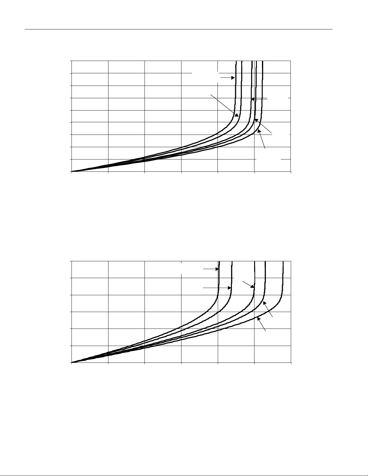
HIG H- LEVEL OUTPUT VO LTAG E
vs
HIGH- LEVEL OUTPUT CURRENT
2
1.8
VDD = 1. 8 V
1.6
1.4
-40oC
1.2
0oC
1
0.8
85oC
0.6
- High-Level Output Voltage -
OH
V
0.4
0.2
125oC
0
0.00 0.20 0.40 0.60 0.80 1.00 1.20 1.40 1.60 1.80
I
- High-Level Output Current - mA
OH
Figure 7.0
HIG H- L EVEL O UTPUT VO LTAGE
vs
HIG H- LEVEL OUTPUT CURRENT
3.5
25oC
3
VDD = 3. 0 V
2.5
2
-40oC
0oC
1.5
25oC85oC
1
- High-Level Output Voltage -
OH
V
0.5
125oC
0
0.00 1.00 2.00 3.00 4.00 5.00 6.00 7.00 8.00
- Hi gh- Le ve l O ut p ut Cur r e nt - mA
I
OH
Figure 8.0
9 of 19
Page 10
1.8
1.6
1.4
1.2
1.0
0.8
DS4802
LOW-LEVEL OUTPUT VOLTAGE
vs
LOW -LEVEL OUTPUT CURRE NT
VDD = 1.8 V
125oC
85oC
25oC
0.6
0.4
- Low-Level Output Voltage - V
OL
V
0.2
-40oC
0.0
0.0 0.5 1.0 1.5 2.0 2.5 3.0
- Low-Level O ut put Curr ent - m A
I
OL
Figure 9.0
LOW-LEVEL O UTPUT VO LT A GE
vs
LOW -LEVE L OUTPUT CURRENT
3.0
VDD = 3.0 V
2.5
2.0
125oC
25oC
85oC
0oC
1.5
0oC
1.0
-40oC
- Low-Level Output Voltage - V
0.5
OL
V
0.0
024681012
I
- Low-Level O ut put Current - m A
OL
Figure 10.0
10 of 19
Page 11

DS4802
A
A
SHORT - CIRCUIT OUTP UT CURRE NT
vs
FREE-AIR TEMPERATURE
3
2
I
OSL
1
VDD = 1. 8 V
0
-1
- Short-Circuit Output Current - m
OS
I
I
OSH
-2
-50 -25 0 25 50 75 100 125
T
- Free- A ir Temper at ur e - oC
A
Figure 11.0
SHORT - CIRCUI T OUTPUT CURRENT
vs
FREE-AIR TEMPERA T URE
12
8
I
OSL
4
VDD = 3.0 V
0
-4
- Short-Circuit Output Current - m
OS
I
I
OSH
-8
-50-25 0 255075100125
T
- Free-Air Temperatur e - oC
A
Figure 12.0
11 of 19
Page 12

B
40
B
DS4802
LA RG E-SI GNA L DIFFERENTIAL VOLTAGE AMPLIFI CATI ON
AND PHASE MARGIN
vs
FREQUENCY
90
20
Phase
A
VD
VDD = 1. 8 V
= 25oC
T
A
= 100K
R
L
= 100pF
C
L
0
- Gain Margin - d
VD
-20
A
-40
1K 10K 100K 1M
f - Frequency - Hz
Figure 13.0
LARGE-SIG NAL DIFFERENTIA L VOLTAGE AMPLIFICA TION
AND PHASE MARGI N
vs
FREQUENCY
40
45
0
-45
Phase Margin - degrees
-90
90
20
Phase
A
VD
0
VDD = 3. 0 V
= 25oC
T
A
= 100K
R
L
= 100pF
C
L
45
0
- Gain Margin - d
VD
A
-20
-40
-45
Phase Margin - degrees
-90
1K 10K 100K 1M
f - Frequency - Hz
Figure 14.0
12 of 19
Page 13

100
80
DS4802
COMMON-MO DE RE JE CT IO N RATIO
vs
FREQUENCY
VDD = 3.0 V
60
VDD = 1.8 V
40
CMRR - Common-Mode Rejection Ratio - dB
20
0
10 100 1K 10K 100K
f - Frequency - Hz
Figure 15.0
SUPPLY-V OLTAG E REJ EC TION RATIO
vs
100
k
80
SVR
FREQUENCY
+
60
40
k
-
SVR
20
- Supply-Voltage Rejection Ratio - dB
SVR
k
0
-20
100 1K 10K 100K
f - Fre quency - Hz
Figure 16.0
13 of 19
Page 14

0.600
0.580
0.560
0.540
0.520
0.500
0.480
0.460
- Output Voltage - V
O
V
0.440
0.420
0.400
0 200 400 600 800 1000
VOLTAGE -FOLLOWER
SMALL-SIGNAL PULSE RESPONSE
t - Time - us
VDD = 1. 8 V
A
= +1
V
= 100K
R
L
C
= 100pF
L
= 25oC
T
A
DS4802
1.100
1.050
1.000
- Output Voltage - V
O
0.950
V
0.900
0 200 400 600 800 1000
Figure 17.0
VOLTAGE-FOLLOWER
SMA L L- SI GNAL PULSE RESPONSE
VDD = 3. 0 V
A
= +1
V
R
= 100K
L
= 100pF
C
L
T
= 25oC
A
t - Time - us
Figure 18.0
14 of 19
Page 15

1.000
0.900
0.800
0.700
0.600
0.500
0.400
0.300
- Output Voltage - V
O
V
0.200
0.100
0.000
0 200 400 600 800 1000
VOLTAGE-FOLLOWER
LA RG E- SI GNAL PULSE RESPONSE
t - Time - us
VDD = 1.8 V
= +1
A
V
R
= 10 0K
L
= 10 0pF
C
L
= 25oC
T
A
DS4802
2.000
VDD = 3.0 V
A
1.750
1.500
= +1
V
R
= 100 K
L
C
= 100 pF
L
T
= 25oC
A
1.250
1.000
- Output Voltage - V
0.750
O
V
0.500
0.250
0 200 400 600 800 1000
Figure 19.0
VOLTAGE-FOLLOWER
LA RGE-SIGNA L PULSE RESPONSE
t - Time - us
Figure 20.0
15 of 19
Page 16

0.600
0.580
0.560
0.540
0.520
0.500
0.480
0.460
- Output Voltage - V
O
V
0.440
0.420
0.400
0 200 400 600 800 1000
INVERTING SMA L L-SI GNAL
PULSE RESPONSE
t - Time - us
VDD = 1. 8 V
= -1
A
V
= 100K
R
L
C
= 100pF
L
= 25oC
T
A
DS4802
1.100
1.050
1.000
- Output Voltage - V
O
0.950
V
0.900
0 200 400 600 800 1000
Figure 21.0
INVERTING SMALL-SI GNA L
PULSE RESPO NSE
VDD = 3.0 V
= -1
A
V
= 100K
R
L
= 100pF
C
L
= 25oC
T
A
t - Time - us
Figure 22.0
16 of 19
Page 17

1.000
0.900
0.800
0.700
0.600
0.500
0.400
0.300
- Output Voltage - V
O
V
0.200
0.100
0.000
0 200 400 600 800 1000
INVERTING L ARGE-SIG NAL
PULSE RESPONSE
t - Time - us
VDD = 1.8 V
= -1
A
V
= 10 0K
R
L
C
= 10 0pF
L
= 25oC
T
A
DS4802
2.000
1.750
1.500
1.250
1.000
0.750
- Output Voltage - V
O
V
0.500
0.250
0 200 400 600 800 1000
Figure 23.0
INVERTI NG LARGE- SIG NAL
PULSE RESP O N SE
VDD = 3.0 V
A
= -1
V
R
= 100K
L
C
= 100pF
L
T
= 25oC
A
t - Time - us
Figure 24.0
17 of 19
Page 18

40
30
20
VIC = 30% V
DS4802
SUPPLY CURRENT
vs
SUPPLY V OLTAG E
DD
125oC
85oC
- Supply Current - uA
DD
I
10
-40oC
0oC
25oC
0
0 0.5 1 1.5 2 2.5 3 3.5 4 4 .5 5
V
- Suplly Voltage - V
DD
Figure 25.0
UNITY-GAIN BANDWIDTH
vs
LOAD CAPACITANCE
40
35
30
25
20
VDD = 3.0 V
R
= 100K
L
= 25oC
T
A
15
10
5
0
10 100 1K 10K
C
- Load Capacitance - p F
L
Figure 26.0
18 of 19
Page 19

70
60
50
40
VDD = 3.0 V
= 100K
R
L
= 25oC
T
A
PHASE M ARGI N
vs
LOAD CAPA CITANCE
R
= 10K R
null
= 4.7K
null
DS4802
30
20
Phase Margin - degrees
10
25
20
15
10
Gain Margin - dB
5
AC
+VDD/2
+
-
-VDD/2
R
NULL
C
R
LOAD
LOAD
R
= 2. 2K
null
R
= 0
null
0
10 100 1K
C
- Load Capacitance - pF
L
Figure 27.0
GAIN MARGIN
vs
LOAD CAPACITA NCE
VDD = 3.0 V
R
= 100K
L
T
= 25oC
A
AC
+VDD/2
+
-
-VDD/2
R
NULL
C
R
LOAD
LOAD
R
null
= 10K
R
null
= 2.2K
R
= 4.7K
null
R
= 0
null
0
10 100 1K
- Load Capacitance - pF
C
L
Figure 28.0
19 of 19
 Loading...