

Page 1
查询DS40MB200供应商
DS40MB200
Dual 4 Gb/s 1:2 Mux/Buffer with Input Equalization and
Output Pre-Emphasis
DS40MB200 Dual 4 Gb/s 1:2 Mux/Buffer with Input Equalization and Output Pre-Emphasis
August 2005
General Description
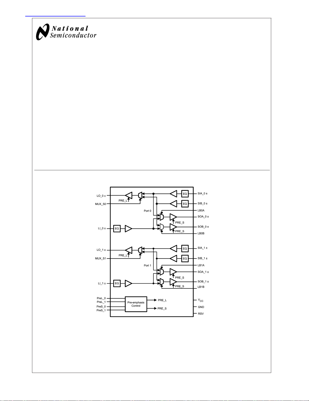
The DS40MB200 is a dual signal conditioning 2:1 multiplexer and 1:2 fan-out buffer designed for use in backplane
redundancy applications. Signal conditioning features include input equalization and programmable output preemphasis that enable data communication in FR4 backplanes up to 4 Gb/s. Each input stage has a fixed equalizer
to reduce ISI distortion from board traces. All output drivers
have 4 selectable steps of pre-emphasis to compensate for
transmission losses from long FR4 backplanes and reduce
deterministic jitter. The pre-emphasis levels can be independently controlled for the line-side and switch-side drivers.
The internal loopback paths from switch-side input to switchside output enable at-speed system testing. All receiver
inputs and driver outputs are internally terminated with 100Ω
differential terminating resistors
Functional Block Diagram
Features
n Dual 2:1 multiplexer and 1:2 buffer
n 1– 4 Gbps fully differential data paths
n Fixed input equalization
n Programmable output pre-emphasis
n Independent switch and line side pre-emphasis controls
n Programmable switch-side loopback mode
n On-chip terminations
n +3.3V supply
n Low power, 1W max
n Lead-less LLP-48 package (7mmx7mmx0.8mm, 0.5mm
pitch)
n 0˚C to +85˚C operating temperature range
20021733
© 2005 National Semiconductor Corporation DS200217 www.national.com
Page 2
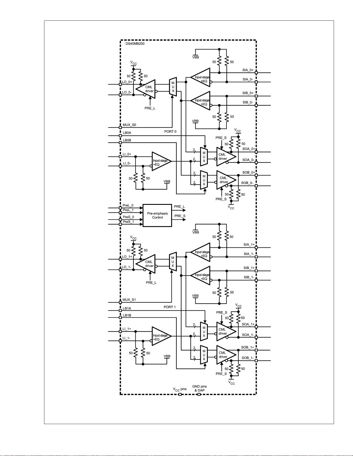
Simplified Block Diagram
DS40MB200
www.national.com 2
20021731
Page 3
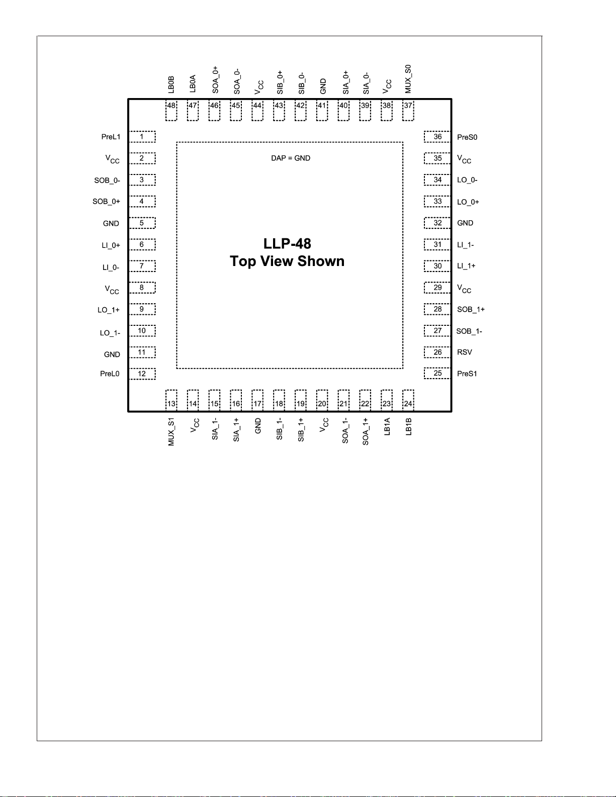
Connection Diagram
DS40MB200
Order number DS40MB200SQ
See NS Package Number SQA48D
20021732
www.national.com3
Page 4
Pin Descriptions
Pin Name
DS40MB200
LINE SIDE HIGH SPEED DIFFERENTIAL IO’s
LI_0+
LI_0−
LO_0+
LO_0−
LI_1+
LI_1−
LO_1+
LO_1−
Pin
Number
6
7
33
34
30
31
9
10
I/O Description
I Inverting and non-inverting differential inputs of port_0 at the line side. LI_0+ and LI_0−
have an internal 50Ω connected to an internal reference voltage.
O Inverting and non-inverting differential outputs of port_0 at the line side. LO_0+ and LO_0−
have an internal 50Ω connected to V
.
CC
I Inverting and non-inverting differential inputs of port_1 at the line side. LI_1+ and LI_1−
have an internal 50Ω connected to an internal reference voltage.
O Inverting and non-inverting differential outputs of port_1 at the line side. LO_1+ and LO_1−
have an internal 50Ω connected to V
.
CC
SWITCH SIDE HIGH SPEED DIFFERENTIAL IO’s
SOA_0+
SOA_0−
SOB_0+
SOB_0−
SIA_0+
SIA_0−
SIB_0+
SIB_0−
SOA_1+
SOA_1−
SOB_1+
SOB_1−
SIA_1+
SIA_1−
SIB_1+
SIB_1−
46
45
40
39
43
42
22
21
28
27
16
15
19
18
O Inverting and non-inverting differential outputs of mux_0 at the switch_A side. SOA_0+ and
SOA_0− have an internal 50Ω connected to V
4
3
O Inverting and non-inverting differential outputs of mux_0 at the switch_B side. SOB_0+ and
SOB_0− have an internal 50Ω connected to VCC.
.
CC
I Inverting and non-inverting differential inputs to the mux_0 at the switch_A side. SIA_0+
and SIA_0− have an internal 50Ω connected to an internal reference voltage.
I Inverting and non-inverting differential inputs to the mux_0 at the switch_B side. SIB_0+
and SIB_0− have an internal 50Ω connected to an internal reference voltage.
O Inverting and non-inverting differential outputs of mux_1 at the switch_A side. SOA_1+ and
SOA_1− have an internal 50Ω connected to V
.
CC
O Inverting and non-inverting differential outputs of mux_1 at the switch_B side. SOB_1+ and
SOB_1− have an internal 50Ω connected to V
.
CC
I Inverting and non-inverting differential inputs to the mux_1 at the switch_A side. SIA_1+
and SIA_1− have an internal 50Ω connected to an internal reference voltage.
I Inverting and non-inverting differential inputs to the mux_1 at the switch_B side. SIB_1+
and SIB_1− have an internal 50Ω connected to an internal reference voltage.
CONTROL (3.3V LVCMOS)
MUX_S0 37 I A logic low at MUX_S0 selects mux_0 to switch B. MUX_S0 is internally pulled high.
Default state for mux_0 is switch A.
MUX_S1 13 A logic low at MUX_S1 selects mux_1 to switch B. MUX_S0 is internally pulled high.
Default state for mux_1 is switch A.
PREL_0
PREL_1
12
I PREL_0 and PREL_1 select the output pre-emphasis of the line side drivers (LO_0
±
1
). PREL_0 and PREL_1 are internally pulled high. See Table 3 for line side
LO_1
pre-emphasis levels.
PRES_0
PRES_1
36
25
I PRES_0 and PRES_1 select the output pre-emphasis of the switch side drivers (SOA_0
±
SOB_0
, SOA_1±and SOB_1±). PRES_0 and PRES_1 are internally pulled high. See
Table 4 for switch side pre-emphasis levels.
LB0A 47 I A logic low at LB0A enables the internal loopback path from SIA_0±to SOA_0±. LB0A is
internally pulled high.
±
LB0B 48 I A logic low at LB0B enables the internal loopback path from SIB_0
to SOB_0±. LB0B is
internally pulled high.
±
LB1A 23 I A logic low at LB1A enables the internal loopback path from SIA_1
to SOA_1±. LB1A is
internally pulled high.
LB1B 24 I A logic low at LB1B enables the internal loopback path from SIB_1±to SOB_1±. LB1B is
internally pulled high.
RSV 26 I Reserve pin to support factory testing. This pin can be left open, or tied to GND, or tied to
GND through an external pull-down resistor.
±
and
±
,
www.national.com 4
Page 5
Pin Descriptions (Continued)
DS40MB200
Pin Name
POWER
V
CC
GND 5, 11, 17,
GND DAP P Die Attach Pad (DAP) is the metal contact at the bottom side, located at the center of the
Note: I = Input, O = Output, P = Power
Pin
Number
2, 8, 14,
20, 29, 35,
38, 44
32, 41
I/O Description
PV
P Ground reference. Each ground pin should be connected to the ground plane through a low
= 3.3V±5%.
CC
Each V
typically with a via located as close as possible to the landing pad of the V
It is recommended to have a 0.01 µF or 0.1 µF, X7R, size-0402 bypass capacitor from
each V
inductance path, typically with a via located as close as possible to the landing pad of the
GND pin.
LLP-48 package. It should be connected to the GND plane with at least 4 via to lower the
ground impedance and improve the thermal performance of the package.
pin should be connected to the VCCplane through a low inductance path,
CC
CC
pin to ground plane.
CC
pin.
Functional Descriptions
The DS40MB200 is a signal conditioning 2:1 multiplexer and a 1:2 buffer designed to support port redundancy up to 4 Gb/s. Each
input stage has a fixed equalizer that provides equalization to compensate about 5 dB of transmission loss from a short backplane
trace (about 10 inches backplane). The output driver has pre-emphasis (driver-side equalization) to compensate the transmission
loss of the backplane that it is driving. The driver conditions the output signal such that the lower frequency and higher frequency
pulses reach approximately the same amplitude at the end of the backplane, and minimize the deterministic jitter caused by the
amplitude disparity. The DS40MB200 provides 4 steps of user-selectable pre-emphasis ranging from 0, -3, -6 and –9 dB to handle
different lengths of backplane. Figure 1 shows a driver pre-emphasis waveform. The pre-emphasis duration is 200ps nominal,
corresponds to 0.75 bit-width at 4 Gb/s. The pre-emphasis levels of switch-side and line-side can be individually programmed.
The high speed inputs are self-biased to about 1.5V and are designed for AC coupling. The inputs are compatible to most AC
coupling differential signals such as LVDS, LVPECL and CML.
TABLE 1. LOGIC TABLE FOR MULTIPLEX CONTROLS
MUX_S0 Mux Function
0 MUX_0 select switch_B input, SIB_0
1 (default) MUX_0 select switch_A input, SIA_0
MUX_S1 Mux Function
0 MUX_1 select switch_B input, SIB_1
1 (default) MUX_1 select switch_A input, SIA_0
TABLE 2. LOGIC TABLE FOR LOOPBACK Controls
LB0A Loopback Function
0 Enable loopback from SIA_0
1 (default) Normal mode. Loopback disabled.
LB0B Loopback Function
0 Enable loopback from SIB_0
1 (default) Normal mode. Loopback disabled.
LB1A Loopback Function
0 Enable loopback from SIA_1
1 (default) Normal mode. Loopback disabled.
LB1B Loopback Function
0 Enable loopback from SIB_1
1 (default) Normal mode. Loopback disabled.
±
to SOA_0±.
±
to SOB_0±.
±
to SOA_1±.
±
to SOB_1±.
±
.
±
.
±
.
±
.
www.national.com5
Page 6

Functional Descriptions (Continued)
TABLE 3. LINE-SIDE PRE-EMPHASIS CONTROLS
DS40MB200
0 0 1200 1200 0 10 inches
0 1 1200 850 −3 20 inches
1 0 1200 600 −6 30 inches
1 1 (default) 1200 426 −9 40 inches
0 0 1200 1200 0 10 inches
0 1 1200 850 −3 20 inches
1 0 1200 600 −6 30 inches
1 1 (default) 1200 426 −9 40 inches
PreL_[1:0]
PreS_[1:0]
Pre-Emphasis Level in
mV
PP
(VODB)
TABLE 4. SWITCH-SIDE PRE-EMPHASIS CONTROLS
Pre-Emphasis Level in
mV
PP
(VODB)
De-Emphasis Level
in mV
PP
(VODPE)
De-Emphasis Level
in mV
PP
(VODPE)
Pre-Emphasis in dB
(VODPE/VODB)
Pre-Emphasis in dB
(VODPE/VODB)
Typical FR4 board
trace
Typical FR4 board
trace
FIGURE 1. Driver Pre-Emphasis Differential Waveform (showing all 4 pre-emphasis steps)
www.national.com 6
20021737
Page 7

DS40MB200
Absolute Maximum Ratings (Note 1)
If Military/Aerospace specified devices are required,
please contact the National Semiconductor Sales Office/
Distributors for availability and specifications.
Supply Voltage (V
) −0.3V to 4V
CC
Thermal Resistance, θ
Thermal Resistance, θ
Thermal Resistance,Φ
ESD Rating HBM, 1.5 kΩ, 100 pF 2.5 kV
ESD Rating Machine Model 250V
CMOS/TTL Input Voltage −0.3V to
+0.3V)
(V
CC
CML Input/Output Voltage −0.3V to
Recommended Operating Ratings
(VCC+0.3V)
Junction Temperature +125˚C
Storage Temperature −65˚C to +150˚C
Lead Temperature
Soldering, 4 sec +260˚C
Thermal Resistance, θ
JA
33.7˚C/W
Supply Voltage (V
CC
Supply Noise Amplitude
10 Hz to 2 GHz
Ambient Temperature 0 85 ˚C
Case Temperature 100 ˚C
Electrical Characteristics
Over recommended operating supply and temperature ranges unless otherwise specified.
Symbol Parameter Conditions Min
LVCMOS DC SPECIFICATIONS
V
IH
V
IL
I
IH
I
IL
R
PU
RECEIVER SPECIFICATIONS
V
ID
V
ICM
R
ITD
R
ITSE
DRIVER SPECIFICATIONS
VODB Output Differential
High Level Input
Voltage
Low Level Input
Voltage
High Level Input
VIN=V
CC
−0.3 0.8 V
Current
Low Level Input
VIN= GND
Current
Pull-High Resistance 35 kΩ
Differential Input
Voltage Range
AC Coupled Differential Signal
Below 1.25 Gb/s
At 1.25 Gbps–3.125 Gbps
Above 3.125 Gbps
This parameter is not production tested.
Common Mode
Voltage at Receiver
Measured at receiver inputs reference to
ground. 1.3 V
Inputs
Input Differential
Termination
Input Termination
(single-end)
Voltage Swing
without
Pre-Emphasis
On-chip differential termination between IN+
or IN−.
On-chip termination IN+ or IN− to GND for
>
frequency
= 100Ω±1%
R
L
100 MHz.
PRES_1=PRES_0=0
PREL_1=PREL_0=0
Driver pre-emphasis disabled.
1000 1200 1400 mV
Running K28.7 pattern at 4 Gbps.
See Figure 5 for test circuit.
JC-top
JC-bottom
JB
20.7˚C/W
5.8˚C/W
18.2˚C/W
Min Typ Max Units
-GND) 3.135 3.3 3.465 V
20 mV
Typ
(Note 2)
2.0
Max Units
V
CC
+0.3
−10 10 µA
75 94 124 µA
100
100
100
1750
1560
1200
mV
mV
mV
84 100 116 Ω
50 Ω
PP
V
P-P
P-P
P-P
P-P
www.national.com7
Page 8

Electrical Characteristics (Continued)
Over recommended operating supply and temperature ranges unless otherwise specified.
Symbol Parameter Conditions Min
DS40MB200
DRIVER SPECIFICATIONS
V
PE
t
PE
R
OTSE
R
OTD
∆R
OTSE
V
OCM
POWER DISSIPATION
P
D
AC CHARACTERISTICS
t
R
t
F
t
PLH
t
PHL
t
SKP
t
SKO
t
SKPP
Output Pre-Emphasis
Voltage Ratio
20*log(VODPE/VODB)
= 100Ω±1%
R
L
Running K28.7 pattern at 4 Gbps
PREx_[1:0]=00
PREx_[1:0]=01
PREx_[1:0]=10
PREx_[1:0]=11
x=S for switch side pre-emphasis control
x=L for line side pre-emphasis control
See Figure 1 on waveform.
See Figure 5 for test circuit.
Pre-Emphasis Width
(Note 8)
Tested at −9 dB pre-emphasis level,
PREx[1:0]=11
x=S for switch side pre-emphasis control
x=L for line side pre-emphasis control
See Figure 4 on measurement condition.
Output Termination On-chip termination from OUT+ or OUT− to
V
CC
Output Differential
Termination
Mis-Match in Output
Termination
On-chip differential termination between OUT+
and OUT−
Mis-match in output terminations at OUT+ and
OUT− 5 %
Resistors
Output Common
Mode Voltage
Power Dissipation VDD= 3.465V
±
All outputs terminated by 100Ω
1%.
PREL_[1:0]=0, PRES_[1:0]=0
7
-1 pattern at 4 Gbps
Differential Low to
High Transition Time
Running PRBS 2
Measured with a clock-like pattern at
100 MHz, between 20% and 80% of the
differential output voltage. Pre-emphasis
Differential High to
Low Transition Time
disabled.
Transition time is measured with fixture as
shown in Figure 5, adjusted to reflect the
transition time at the output pins.
Differential Low to
High Propagation
Measured at 50% differential voltage from
input to output. 0.5 2 ns
Delay
Differential High to
Low Propagation
Delay
Pulse Skew (Note 8) |t
Output Skew
(Notes 7, 8)
Part-to-Part Skew
(Note 8)
PHL–tPLH
Difference in propagation delay among data
paths in the same device.
Difference in propagation delay between the
same output from devices operating under
|20ps
identical condition.
Typ
(Note 2)
0
−3
−6
−9
Max Units
dB
dB
dB
dB
125 200 250 ps
42 50 58 Ω
100 Ω
2.7 V
1W
80 ps
80 ps
0.5 2 ns
200 ps
500 ps
www.national.com 8
Page 9

Electrical Characteristics (Continued)
Over recommended operating supply and temperature ranges unless otherwise specified.
Symbol Parameter Conditions Min
AC CHARACTERISTICS
t
SM
Mux Switch Time Measured from VIHor VILof the mux-control
or loopback control to 50% of the valid
differential output.
RJ Device Random Jitter
(Note 5) (Note 8)
See Figure 5 for test circuit.
Alternating-1-0 pattern.
Pre-emphasis disabled.
At 1.25 Gbps
At 4 Gbps
DJ Device Deterministic
Jitter (Note 6) (Note
8)
DR
MAX
Maximum Data Rate
(Note 8)
Note 1: “Absolute Maximum Ratings” are the ratings beyond which the safety of the device cannot be guaranteed. They are not meant to imply that the device
should be operated at these limits.
Note 2: Typical parameters measured at V
Note 3: IN+ and IN− are generic names refer to one of the many pairs of complimentary inputs of the DS40MB200. OUT+ and OUT− are generic names refer to
one of the many pairs of the complimentary outputs of the DS40MB200. Differential input voltage V
defined as |OUT+–OUT−|.
Note 4: K28.7 pattern is a 10-bit repeating pattern of K28.7 code group {001111 1000}
K28.5 pattern is a 20-bit repeating pattern of +K28.5 and −K28.5 code groups {110000 0101 001111 1010}
Note 5: Device output random jitter is a measurement of the random jitter contribution from the device. It is derived by the equation sqrt(RJ
RJ
is the total random jitter measured at the output of the device in psrms, RJINis the random jitter of the pattern generator driving the device.
OUT
Note 6: Device output deterministic jitter is a measurement of the deterministic jitter contribution from the device. It is derived by the equation (DJ
DJ
is the total peak-to-peak deterministic jitter measured at the output of the device in pspp, DJINis the peak-to-peak deterministic jitter of the pattern generator
OUT
driving the device.
Note 7: t
between port 0 and port 1. An example is the output skew among data paths from SIA_0
Another example is the output skew among data paths from LI_0
delay skew of the loopback paths of the same port and between similar data paths between port 0 and port 1. An example is the output skew among data paths
SIA_0
Note 8: Guaranteed by desigh and characterization using statistical analysis.
is the magnitude difference in the propagation delays among data paths between switch A and switch B of the same port and similar data paths
SKO
±
to SOA_0±, SIB_0±to SOB_0±, SIA_1±to SOA_1±and SIB_1±to SOB_1±.
See Figure 5 for test circuit.
Pre-emphasis disabled.
At 4 Gbps, PRBS7 pattern 30 pspp
Tested with alternating-1-0 pattern
= 3.3V, TA= 25˚C. They are for reference purposes and are not production-tested.
CC
ID
±
±
to SOA_0±, LI_0±to SOB_0±, LI_1±to SOA_1±and LI_1±to SOB_1±.t
to LO_0±, SIB_0±to LO_0±, SIA_1±to LO_1±and SIB_1±to LO_1±.
4 Gbps
is defined as |IN+–IN−|. Differential output voltage VODis
Typ
(Note 2)
Max Units
1.8 6 ns
2
2
2
–RJ
OUT
–DJIN), where
OUT
also refers to the
SKO
psrms
psrms
2
), where
IN
DS40MB200
Timing Diagrams
20021736
FIGURE 2. Driver Output Transition Time
www.national.com9
Page 10

Timing Diagrams (Continued)
DS40MB200
20021735
FIGURE 3. Propagation Delay from input to output
FIGURE 4. Test condition for output pre-emphasis duration
FIGURE 5. AC Test Circuit
The DS40MB200 input equalizer provides equalization to
compensate about 5 dB of transmission loss from a short
backplane transmission line. For characterization purposes,
a 25-inch FR4 coupled micro-strip board trace is used in
place of the short backplane link. The 25-inch microstrip
board trace has approximately 5 dB of attenuation between
20021739
20021734
375 MHz and 1.875 GHz, representing closely the transmission loss of the short backplane transmission line. The 25inch microstrip is connected between the pattern generator
and the differential inputs of the DS40MB200 for AC measurements.
www.national.com 10
Page 11

Timing Diagrams (Continued)
DS40MB200
Trace Length
Finished Trace
Width W
Separation between
Traces Dielectric Height H
Dielectric Constant
e
R
Loss Tangent
25 inches 8.5 mil 11.5 mil 6 mil 3.8 0.022
FIGURE 6. Data input and output eye patterns with driver set to 0 dB pre-emphasis
20021742
www.national.com11
Page 12

Timing Diagrams (Continued)
DS40MB200
20021743
FIGURE 7. Data input and output eye patterns with driver set to 9dB pre-emphasis
www.national.com 12
Page 13

Application Information
DS40MB200
FIGURE 8. Application diagram (showing data paths of port 0)
20021740
www.national.com13
Page 14

Physical Dimensions inches (millimeters) unless otherwise noted
LLP-48 Package
National does not assume any responsibility for use of any circuitry described, no circuit patent licenses are implied and National reserves
the right at any time without notice to change said circuitry and specifications.
For the most current product information visit us at www.national.com.
LIFE SUPPORT POLICY
NATIONAL’S PRODUCTS ARE NOT AUTHORIZED FOR USE AS CRITICAL COMPONENTS IN LIFE SUPPORT DEVICES OR SYSTEMS
WITHOUT THE EXPRESS WRITTEN APPROVAL OF THE PRESIDENT AND GENERAL COUNSEL OF NATIONAL SEMICONDUCTOR
CORPORATION. As used herein:
1. Life support devices or systems are devices or systems
which, (a) are intended for surgical implant into the body, or
(b) support or sustain life, and whose failure to perform when
properly used in accordance with instructions for use
2. A critical component is any component of a life support
device or system whose failure to perform can be reasonably
expected to cause the failure of the life support device or
system, or to affect its safety or effectiveness.
provided in the labeling, can be reasonably expected to result
in a significant injury to the user.
BANNED SUBSTANCE COMPLIANCE
National Semiconductor manufactures products and uses packing materials that meet the provisions of the Customer Products
Stewardship Specification (CSP-9-111C2) and the Banned Substances and Materials of Interest Specification (CSP-9-111S2) and contain
no ‘‘Banned Substances’’ as defined in CSP-9-111S2.
Leadfree products are RoHS compliant.
DS40MB200 Dual 4 Gb/s 1:2 Mux/Buffer with Input Equalization and Output Pre-Emphasis
National Semiconductor
Americas Customer
Support Center
Email: new.feedback@nsc.com
Tel: 1-800-272-9959
www.national.com
National Semiconductor
Europe Customer Support Center
Fax: +49 (0) 180-530 85 86
Email: europe.support@nsc.com
Deutsch Tel: +49 (0) 69 9508 6208
English Tel: +44 (0) 870 24 0 2171
Français Tel: +33 (0) 1 41 91 8790
National Semiconductor
Asia Pacific Customer
Support Center
Email: ap.support@nsc.com
National Semiconductor
Japan Customer Support Center
Fax: 81-3-5639-7507
Email: jpn.feedback@nsc.com
Tel: 81-3-5639-7560
 Loading...