

Page 1
July 2007
DS38EP100
1 to 5 Gbps, Power-Saver Equalizer for Backplanes and
Cables
General Description
National’s Power-saver equalizer compensates for transmission medium losses and minimizes medium-induced deterministic jitter. Performance is guaranteed over the full range
of 1 to 5 Gbps. The DS38EP100 requires no power to operate.
The equalizer operates anywhere in the data path to minimize
media-induced deterministic jitter in both FR4 and cable applications. Symmetric I/O structures support full duplex or half
duplex applications. Linear compensation is provided independent of line coding or protocol. The device is ideal for both
bi-level and multi-level signaling.
The equalizer is available in a 6 pin leadless LLP package
with a space saving 2.2 mm X 2.5 mm footprint. This tiny
package provides maximum flexibility in placement and routing of the Power-saver equalizer.
Features
■
1 to 5 Gbps Operation
■
No Power or Ground Required
■
Equalization effective anywhere in data path
■
Equalizes CML, LV-PECL, LVDS signals
■
Symmetric I/O structures provide equal boost for bidirectional operation
■
7 dB Maximum Boost
■
Code independent, 8b/10b or Scrambled
■
Supports both bi-level and multi-level signaling
■
Extends reach over backplanes and cables
■
Compatible with PCI-Express Gen1 and Gen2
■
Compatible with XAUI
■
Operates in series with existing active Equalizer
■
Easy to handle 6 pin LLP
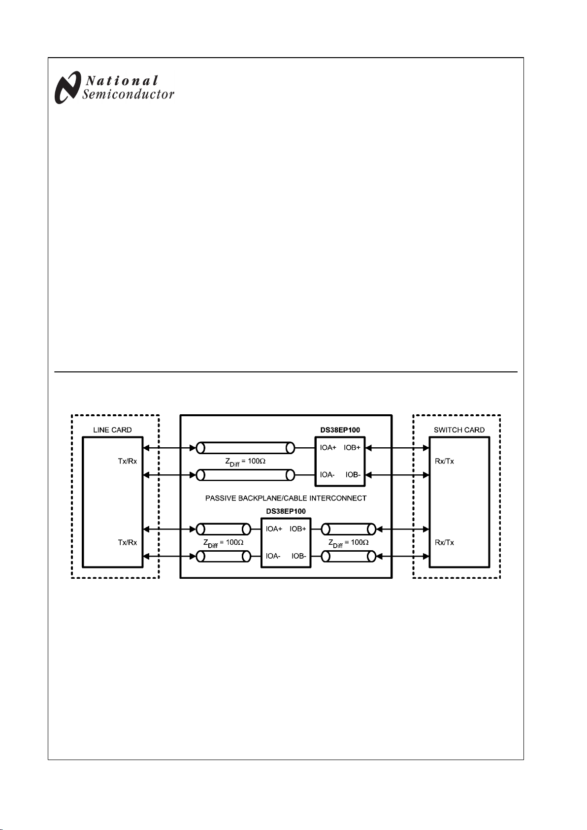
Simplified Application Diagram
30029201
Note:
The DS38EP100 provides the flexibility of passing the data from either side of the device. It can be placed anywhere in the data path..
© 2007 National Semiconductor Corporation 300292 www.national.com
DS38EP100 1 to 5 Gbps, Power-Saver Equalizer for Backplanes and Cables
Page 2
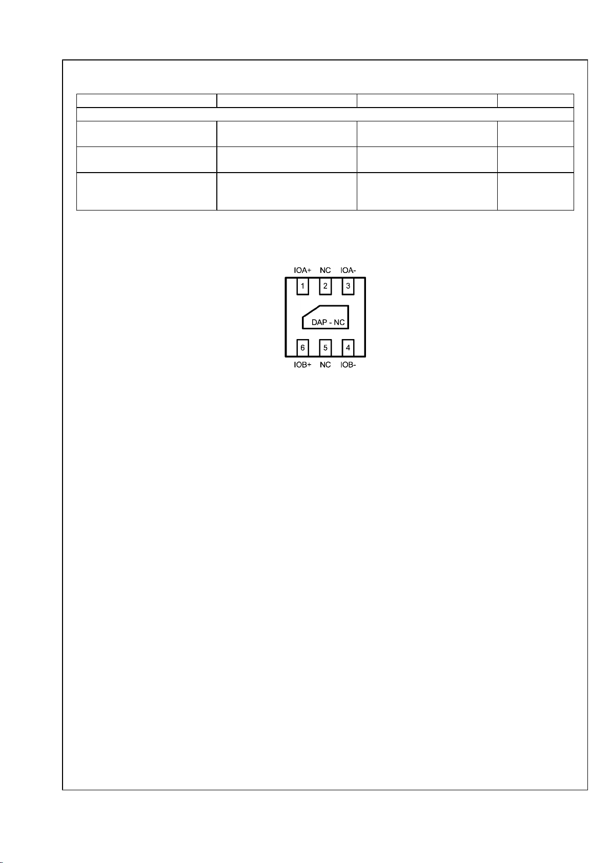
Pin Descriptions
Pin Name Pin Number I/O, Type Description
High Speed Differential I/O
IOAIOA+
3
1
I/O Symmetric
differential I/O.
IOBIOB+
4
6
I/O Symmetric
differential I/O.
NC
Exposed
Pad
2, 5
DAP
N/A Reserved.
Do not connect.
Note:
I = Input / O = Output
Pin Diagram
30029205
Bottom View shown
2.2mm x 2.5mm 6-Pin LLP Package
Order number DS38EP100
www.national.com 2
DS38EP100
Page 3
Absolute Maximum Ratings (Note 1)
If Military/Aerospace specified devices are required,
please contact the National Semiconductor Sales Office/
Distributors for availability and specifications.
INPUT/OUTPUT
(IOA+ and IOB+) or (IOA- and IOB-) +2V
(IOA+ and IOA-) or (IOB+ and IOB-) +4V
(IOA+ and IOB-) or (IOA- and IOB+) +4V
Junction Temperature +150°C
Storage Temperature −65°C to +150°C
Lead Temperature
Soldering, 4 sec +260°C
ESD Rating
HBM, 1.5 kΩ, 100 pF 1.3kV
Recommended Operating
Conditions
Min Typ Max Units
Operating Temperature −40 25 +85 °C
Bit Rate 1 5 Gbps
Electrical Characteristics (Note 6) Over recommended operating conditions unless other specified. All
parameters are guaranteed by test, statistical analysis or design.
Symbol Parameter Conditions Min
Typ
(Note 2)
Max Units
V
IN
Input voltage swing See (Note 3)
1000 3600 mVp-p
Equalization 2.5 GHz relative to 100MHz 6 dB
R
LI
Differential input return
loss
100 MHz – 2.5 GHz, with fixture's effect deembedded
15 dB
R
LO
Differential output
return loss
100 MHz – 2.5 GHz, with fixture's effect deembedded. IOA+,or IOB+ = static high.
15 dB
R
IN
Input Impedance
Differential across IOA+ and IOA-, or IOB+ and
IOB-, ZLOAD = 100Ω
100
Ω
R
O
Output Impedance
Differential across IOA+ and IOA-, or IOB+ and
IOB-, ZSOURCE = 100Ω
100
Ω
Through Response Relative to ideal load, see Figure 2 for setup See Figure 3 and Table 1 for limits
R1
Resistance IOA+ to
IOA- and IOB+ to IOB- No load, high impedance on all ports
150
Ω
R2
Resistance IOA+ to
IOB+ and IOA- to IOB- No load, high impedance on all ports
50
Ω
R3
Resistance IOA+ to
IOB- and IOA- to IOB+ No load, high impedance on all ports
150
Ω
DC Gain
Z
LOAD = 100Ω
0.4
(IOA/IOB or IOB/IOA)
DJ1
Residual deterministic
jitter
2.5 Gbps, 40 in of 6mil microstrip FR4
0.1 UIp-p
See (Note 4)
DJ2
Residual deterministic
jitter
3.125 Gbps, 40 in of 6mil microstrip FR4
0.1 0.15 UIp-p
See (Notes 4, 5)
DJ3
Residual deterministic
jitter
3.8 Gbps, 40 in of 6mil microstrip FR4
0.1 0.15 UIp-p
See (Notes 4, 5)
DJ4
Residual deterministic
jitter
5 Gbps, 30 in of 6mil microstrip FR4
0.1 UIp-p
See (Note 4)
3 www.national.com
DS38EP100
Page 4

Note 1: “Absolute Maximum Ratings” indicate limits beyond which damage to the device may occur, including inoperability and degradation of device reliability
and/or performance. Functional operation of the device and/or non-degradation at the Absolute Maximum Ratings or other conditions beyond those indicated in
the Recommended Operating Conditions is not implied. The Recommended Operating Conditions indicate conditions at which the device is functional and the
device should not be operated beyond such conditions.
Note 2: Typical values represent most likely parametric norms, TA = +25 degC, and at the Recommended Operating Conditions at the time of product
characterization and are not guaranteed.
Note 3: Differential signal to Equalizer, measured at the input to a transmission line, see point A of Figure 1. The transmission line is Z0 = 100Ω, 6-mil, microstrip
in FR4 material.
Note 4: Deterministic jitter is measured at the differential outputs (point C of Figure 1), minus the deterministic jitter before the test channel (point A of Figure 1).
Test pattern: PRBS- 7 .
Note 5: Specification is guaranteed by characterization and is not tested in production.
Note 6: The Electrical Characteristics tables list guaranteed specifications under the listed Recommended Operating Conditions except as otherwise modified
or specified by the Electrical Characteristics Conditions and/or Notes. Typical specifications are estimations only and are not guaranteed.
www.national.com 4
DS38EP100
Page 5
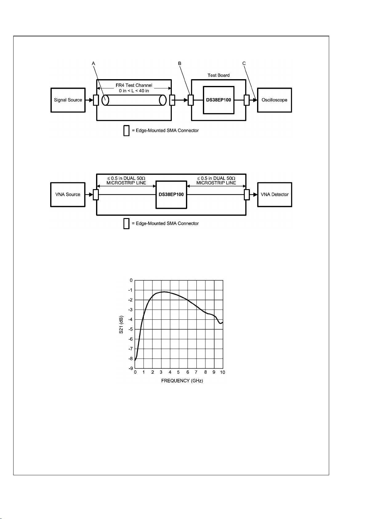
Test Setup Diagrams
30029203
FIGURE 1. Transient Test Setup Diagram
30029204
FIGURE 2. Frequency Response Test Circuit
Typical Equalizer Transfer Function
30029206
FIGURE 3. Typical Equalizer Transfer Function
5 www.national.com
DS38EP100
Page 6

TABLE 1. Typical Through Response
Frequency (GHz) DS38EP100 Attenuation Typ (dB)
0.1 -7.98
0.5 -5.93
1 -3.53
1.5 -2.25
2 -1.58
3 -1.14
4 -1.26
5 -1.54
6 -1.99
7 -2.62
8 -3.26
9 -3.61
10 -4.26
Block Diagram
30029202
FIGURE 4. Simplified Block Diagram
www.national.com 6
DS38EP100
Page 7

Application Information
DS38EP100 DEVICE DESCRIPTION
The DS38EP100 Power-Saver equalizer is a passive network
circuit composed of resistive, capacitive, and inductive components (See Figure 4). A differential bridged T-network compensates for the transmission medium losses and minimizes
medium-induced deterministic jitter with FR4 and cables. The
equalizer attenuates low frequency signals and is a bandpass
filter at the resonant frequency. The response is linear and
symmetric.
I/O TERMINATIONS
The DS38EP100 I/O impedance is 100Ω differential. The
equalizer is designed for 100Ω-balanced differential signals
and is not intended for single-ended transmission.
LINEAR COMPENSATION
The unique linear compensation feature of the DS38EP100
combined with the tiny package allows maximum flexibility in
placement. The equalizer can be placed anywhere in the data
path and will provide the same compensation at the receiving
circuit. (See Simplified Application Diagram)
SYMMETRIC I/O STRUCTURES
The symmetry of the passive equalization network allows bidirectional operation. Signals receive equal compensation
regardless of the direction of data flow. (See Figure 4).
PCB LAYOUT CONSIDERATIONS FOR DIFFERENTIAL
PAIRS AND NO CONNECT PADS
The differential I/Os must have a controlled differential
impedance of 100Ω. It is preferable to route all differential
lines exclusively on one layer of the board. The use of vias
should be avoided if possible. If vias must be used, they
should be used sparingly and must be placed symmetrically
for each side of a given differential pair. Differential signals
should be routed away from other signals and noise sources
on the printed circuit board. Pin 2, Pin 5, and the center DAP
have to be left as a no connect. Therefore, do not connect the
landing pads of these pins to the power or ground plane. See
AN-1187 for additional information on the LLP package.
7 www.national.com
DS38EP100
Page 8

Typical Performance Characteristics
30029207
Residual Deterministic Jitter vs. FR4 Length
30029208
Residual Deterministic Jitter vs. FR4 Length
30029209
Eye Height vs. FR4 Length
30029210
Eye Height vs. FR4 Length
www.national.com 8
DS38EP100
Page 9

Typical Eye Diagrams — Includes Transmitter Setup, Interconnect, and
Device Total Jitter
30029211
FIGURE 5. Unequalized Signal (40in FR4, 2.5Gbps,
PRBS7)
30029212
FIGURE 6. Equalized Signal (40in FR4, 2.5Gbps, PRBS7)
30029213
FIGURE 7. Equalized Signal (Zoom) (40in FR4, 2.5Gbps,
PRBS7)
30029214
FIGURE 8. Unequalized Signal (40in FR4, 3.125Gbps,
PRBS7)
9 www.national.com
DS38EP100
Page 10

30029215
FIGURE 9. Equalized Signal (40in FR4, 3.125Gbps,
PRBS7)
30029216
FIGURE 10. Equalized Signal (Zoom) (40in FR4,
3.125Gbps, PRBS7)
30029217
FIGURE 11. Unequalized Signal (40in FR4, 3.8Gbps,
PRBS7)
30029218
FIGURE 12. Equalized Signal (40in FR4, 3.8Gbps, PRBS7)
30029219
FIGURE 13. Equalized Signal (Zoom) (40in FR4, 3.8Gbps,
PRBS7)
30029220
FIGURE 14. Unequalized Signal (30in FR4, 4.25Gbps,
PRBS7)
www.national.com 10
DS38EP100
Page 11

30029221
FIGURE 15. Equalized Signal (30in FR4, 4.25Gbps,
PRBS7)
30029222
FIGURE 16. Equalized Signal (Zoom) (30in FR4,
4.25Gbps, PRBS7)
30029223
FIGURE 17. Unequalized Signal (30in FR4, 5Gbps,
PRBS7)
30029224
FIGURE 18. Equalized Signal (30in FR4, 5Gbps, PRBS7)
30029225
FIGURE 19. Equalized Signal (Zoom) (30in FR4, 5Gbps,
PRBS7)
30029226
FIGURE 20. Unequalized Signal (34in Tyco XAUI
Backplane, 3.125Gbps, PRBS7)
11 www.national.com
DS38EP100
Page 12

30029227
FIGURE 21. Equalized Signal (34in Tyco XAUI Backplane,
3.125Gbps, PRBS7)
30029228
FIGURE 22. Equalized Signal (Zoom) (34in Tyco XAUI
Backplane, 3.125Gbps, PRBS7)
30029229
FIGURE 23. Unequalized Signal (5m 28AWG HDMI Cable,
3.4Gbps, PRBS7)
30029230
FIGURE 24. Equalized Signal (5m 28AWG HDMI Cable,
3.4Gbps, PRBS7)
30029231
FIGURE 25. Equalized Signal (Zoom) (5m 28AWG HDMI
Cable, 3.4Gbps, PRBS7)
30029232
FIGURE 26. Unequalized Signal (10m 26AWG HDMI
Cable, 2.25Gbps, PRBS7)
www.national.com 12
DS38EP100
Page 13

30029233
FIGURE 27. Equalized Signal (10m 26AWG HDMI Cable,
2.25Gbps, PRBS7)
30029234
FIGURE 28. Equalized Signal (Zoom) (10m 26AWG HDMI
Cable, 2.25Gbps, PRBS7)
30029235
FIGURE 29. Unequalized Signal (10m 24AWG PCIe Cable,
2.5Gbps, PRBS7)
30029236
FIGURE 30. Equalized Signal (10m 24AWG PCIe Cable,
2.5Gbps, PRBS7)
30029237
FIGURE 31. Equalized Signal (Zoom) (10m 24AWG PCIe
Cable, 2.5Gbps, PRBS7)
30029238
FIGURE 32. Unequalized Signal (10m 24AWG PCIe Cable,
5Gbps, PRBS7)
13 www.national.com
DS38EP100
Page 14

30029239
FIGURE 33. Equalized Signal (10m 24AWG PCIe Cable,
5Gbps, PRBS7)
30029240
FIGURE 34. Equalized Signal (Zoom) (10m 24AWG PCIe
Cable, 5Gbps, PRBS7)
www.national.com 14
DS38EP100
Page 15

Physical Dimensions inches (millimeters) unless otherwise noted
Order number DS38EP100
See NS Package SDB06A
15 www.national.com
DS38EP100
Page 16

Notes
DS38EP100 1 to 5 Gbps, Power-Saver Equalizer for Backplanes and Cables
THE CONTENTS OF THIS DOCUMENT ARE PROVIDED IN CONNECTION WITH NATIONAL SEMICONDUCTOR CORPORATION
(“NATIONAL”) PRODUCTS. NATIONAL MAKES NO REPRESENTATIONS OR WARRANTIES WITH RESPECT TO THE ACCURACY
OR COMPLETENESS OF THE CONTENTS OF THIS PUBLICATION AND RESERVES THE RIGHT TO MAKE CHANGES TO
SPECIFICATIONS AND PRODUCT DESCRIPTIONS AT ANY TIME WITHOUT NOTICE. NO LICENSE, WHETHER EXPRESS,
IMPLIED, ARISING BY ESTOPPEL OR OTHERWISE, TO ANY INTELLECTUAL PROPERTY RIGHTS IS GRANTED BY THIS
DOCUMENT.
TESTING AND OTHER QUALITY CONTROLS ARE USED TO THE EXTENT NATIONAL DEEMS NECESSARY TO SUPPORT
NATIONAL’S PRODUCT WARRANTY. EXCEPT WHERE MANDATED BY GOVERNMENT REQUIREMENTS, TESTING OF ALL
PARAMETERS OF EACH PRODUCT IS NOT NECESSARILY PERFORMED. NATIONAL ASSUMES NO LIABILITY FOR
APPLICATIONS ASSISTANCE OR BUYER PRODUCT DESIGN. BUYERS ARE RESPONSIBLE FOR THEIR PRODUCTS AND
APPLICATIONS USING NATIONAL COMPONENTS. PRIOR TO USING OR DISTRIBUTING ANY PRODUCTS THAT INCLUDE
NATIONAL COMPONENTS, BUYERS SHOULD PROVIDE ADEQUATE DESIGN, TESTING AND OPERATING SAFEGUARDS.
EXCEPT AS PROVIDED IN NATIONAL’S TERMS AND CONDITIONS OF SALE FOR SUCH PRODUCTS, NATIONAL ASSUMES NO
LIABILITY WHATSOEVER, AND NATIONAL DISCLAIMS ANY EXPRESS OR IMPLIED WARRANTY RELATING TO THE SALE
AND/OR USE OF NATIONAL PRODUCTS INCLUDING LIABILITY OR WARRANTIES RELATING TO FITNESS FOR A PARTICULAR
PURPOSE, MERCHANTABILITY, OR INFRINGEMENT OF ANY PATENT, COPYRIGHT OR OTHER INTELLECTUAL PROPERTY
RIGHT.
LIFE SUPPORT POLICY
NATIONAL’S PRODUCTS ARE NOT AUTHORIZED FOR USE AS CRITICAL COMPONENTS IN LIFE SUPPORT DEVICES OR
SYSTEMS WITHOUT THE EXPRESS PRIOR WRITTEN APPROVAL OF THE CHIEF EXECUTIVE OFFICER AND GENERAL
COUNSEL OF NATIONAL SEMICONDUCTOR CORPORATION. As used herein:
Life support devices or systems are devices which (a) are intended for surgical implant into the body, or (b) support or sustain life and
whose failure to perform when properly used in accordance with instructions for use provided in the labeling can be reasonably expected
to result in a significant injury to the user. A critical component is any component in a life support device or system whose failure to perform
can be reasonably expected to cause the failure of the life support device or system or to affect its safety or effectiveness.
National Semiconductor and the National Semiconductor logo are registered trademarks of National Semiconductor Corporation. All other
brand or product names may be trademarks or registered trademarks of their respective holders.
Copyright© 2007 National Semiconductor Corporation
For the most current product information visit us at www.national.com
National Semiconductor
Americas Customer
Support Center
Email:
new.feedback@nsc.com
Tel: 1-800-272-9959
National Semiconductor Europe
Customer Support Center
Fax: +49 (0) 180-530-85-86
Email: europe.support@nsc.com
Deutsch Tel: +49 (0) 69 9508 6208
English Tel: +49 (0) 870 24 0 2171
Français Tel: +33 (0) 1 41 91 8790
National Semiconductor Asia
Pacific Customer Support Center
Email: ap.support@nsc.com
National Semiconductor Japan
Customer Support Center
Fax: 81-3-5639-7507
Email: jpn.feedback@nsc.com
Tel: 81-3-5639-7560
www.national.com
 Loading...