

Page 1
DS36C280
Slew Rate Controlled CMOS EIA-RS-485 Transceiver
General Description
The DS36C280 is a low power differential bus/line transceiver designed to meet the requirements of RS-485 Standard for multipoint data transmission. In addition, it is compatible with TIA/EIA-422-B.
The slew ratecontrol feature allows the user to set the driver
rise and fall times by using an external resistor. Controlled
edge rates can reduce switching EMI.
The CMOS design offers significant power savings over its
bipolar andALS counterparts without sacrificing ruggedness
against ESD damage. The device is ideal for use in battery
powered or power conscious applications. I
CC
is specified at
500 µA maximum.
The driver and receiver outputs feature TRI-STATE
®
capability.The driver outputs operate over the entire common mode
range of −7V to +12V. Bus contention or fault situations are
handled by a thermal shutdown circuit, which forces the
driver outputs into the high impedance state.
The receiver incorporates a fail safe circuit which guarantees
a high output state when the inputs are left open (Note 1) .
Features
n 100%RS-485 compliant
— Guaranteed RS-485 device interoperation
n Low power CMOS design: I
CC
500 µA max
n Adjustable slew rate control
— Minimizes EMI affects
n Built-in power up/down glitch-free circuitry
— Permits live transceiver insertion/displacement
n DIP and SOIC packages available
n Industrial temperature range: −40˚C to +85˚C
n On-board thermal shutdown circuitry
— Prevents damage to the device in the event of
excessive power dissipation
n Wide common mode range: −7V to +12V
n Receiver open input fail-safe (Note 1)
n
1
⁄4unit load (DS36C280): ≥128 nodes
n
1
⁄2unit load (DS36C280T): ≥64 nodes
n ESD (human body model): ≥2kV
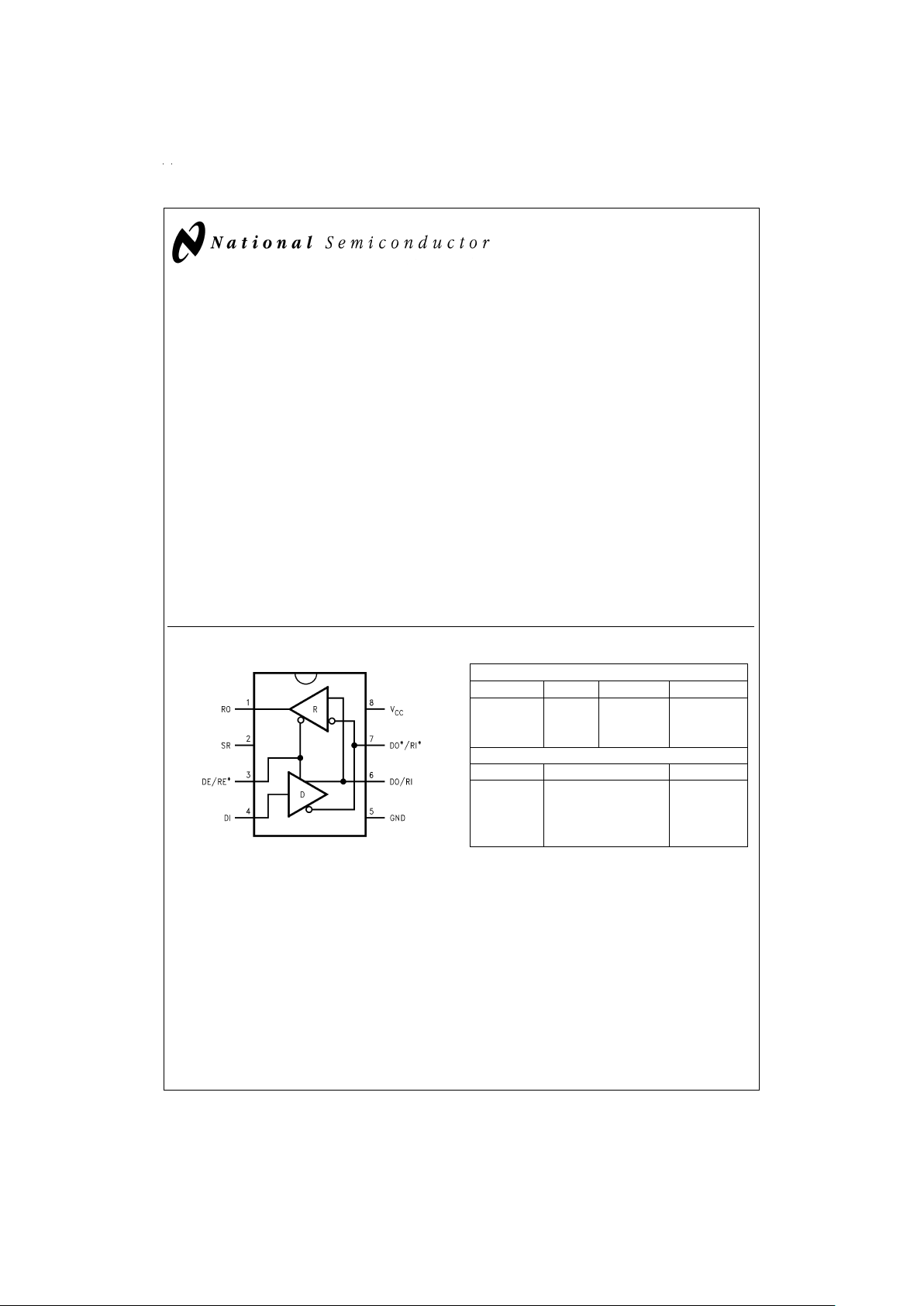
Connection and Logic Diagram Truth Table
DRIVER SECTION
DE/RE* DI DO/RI DO*/RI*
HHH L
HLL H
LXZ Z
RECEIVER SECTION
DE/RE* RI-RI* RO
L ≥+0.2V H
L ≤−0.2V L
HX Z
L OPEN (Note 1) H
Note 1: Non-terminated, Open Inputs only
TRI-STATE®is a registered trademark of National Semiconductor Corporation.
DS012052-1
Order Number DS36C280TM, DS36C280TN
DS36C280M and DS36C280N
See NS Package Number M08A or N08E
July 1998
DS36C280 Slew Rate Controlled CMOS EIA-RS-485 Transceiver
© 1999 National Semiconductor Corporation DS012052 www.national.com
Page 2
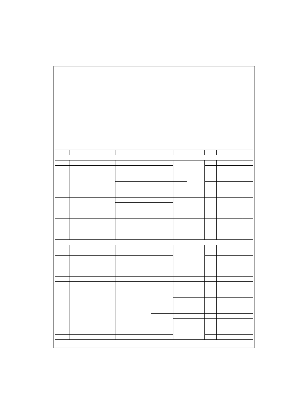
Absolute Maximum Ratings (Note 2)
If Military/Aerospace specified devices are required,
please contact the National Semiconductor Sales Office/
Distributors for availability and specifications.
Supply Voltage (V
CC
) +12V
Input Voltage (DE/RE*, & DI) −0.5V to (V
CC
+0.5V)
Common Mode (V
CM
)
Driver Output/Receiver Input
±
15V
Input Voltage (DO/RI, DO*/RI*)
±
14V
Receiver Output Voltage −0.5V to (V
CC
+0.5V)
Maximum Package Power Dissipation
@
+25˚C
M Package 1190 mV, derate 9.5 mW/˚C above +25˚C
N Package 794 mV, derate 6.0 mW/˚C above +25˚C
Storage Temperature Range −65˚C to +150˚C
Lead Temperature +260˚C
(Soldering 4 sec.)
Recommended Operating
Conditions
Min Typ Max Units
Supply Voltage (V
CC
) +4.75 +5.0 +5.25 V
Bus Voltage −7 +12 V
Operating Free Air Temperature (T
A
)
DS36C280T −40 +25 +85 ˚C
DS36C280 0 +25 +70 ˚C
Electrical Characteristics (Notes 3, 4)
Over Supply Voltage and Operating Temperature ranges, unless otherwise specified
Symbol Parameter Conditions Reference Min Typ Max Units
DIFFERENTIAL DRIVER CHARACTERISTICS
V
OD1
Differential Output Voltage IO= 0 mA (No Load)
(422)
(485)
1.5 5.0 V
V
OD0
Output Voltage IO= 0 mA 0 5.0 V
V
OD0*
Output Voltage (Output to GND) 0 5.0 V
V
OD2
Differential Output Voltage
(Termination Load)
RL=50Ω (422)
Figure 1
2.0 2.8 V
R
L
=27Ω (485) 1.5 2.3 5.0 V
∆V
OD2
Balance of V
OD2
RL=27Ωor 50Ω (Note 5) −0.2 0.1 +0.2 V
|V
OD2−VOD2*
| (422, 485)
V
OD3
Differential Output Voltage
(Full Load)
R1=54Ω,R2=375Ω
Figure 2
1.5 2.0 5.0 V
V
TEST
= −7V to +12V
V
OC
Driver Common Mode
Output Voltage
RL=27Ω (485)
Figure 1
0 3.0 V
R
L
=50Ω (422) 0 3.0 V
∆V
OC
Balance of V
OC
RL=27Ωor (Note 5) −0.2 +0.2 V
|V
OC−VOC*
|R
L
=50Ω (422, 485)
I
OSD
Driver Output Short-Circuit
Current
VO= +12V (485)
Figure 4
200 +250 mA
V
O
= −7V (485) −190 −250 mA
RECEIVER CHARACTERISTICS
V
TH
Differential Input High
Threshold Voltage
VO=VOH,IO= −0.4 mA
(Note 6)
(422, 485)
+0.035 +0.2 V
−7V ≤ V
CM
≤ +12V
V
TL
Differential Input Low
Threshold Voltage
VO=VOL,IO= 0.4 mA −0.2 −0.035 V
−7V ≤ V
CM
≤ +12V
V
HST
Hysteresis VCM=0V 70 mV
R
IN
Input Resistance −7V ≤ VCM≤ +12V DS36C280T 24 68 kΩ
R
IN
Input Resistance −7V ≤ VCM≤ +12V DS36C280 48 68 kΩ
I
IN
Line Input Current
(Note 8)
Other Input = 0V DS36C280 VIN= +12V 0 0.19 0.25 mA
DE=V
IL
,RE*=V
IL
VIN= −7V 0 −0.1 −0.2 mA
V
CC
= 4.75 to 5.25 DS36C280T VIN= +12V 0 0.19 0.5 mA
or 0V V
IN
= −7V 0 −0.1 −0.4 mA
I
ING
Line Input Current
Glitch (Note 8)
Other Input = 0V DS36C280 VIN= +12V 0 0.19 0.25 mA
DE=V
IL
,RE*=V
IL
VIN= −7V 0 −0.1 −0.2 mA
V
CC
= +3.0V DS36C280T VIN= +12V 0 0.19 0.5 mA
or 0V T
A
= 25˚C VIN= −7V 0 −0.1 −0.4 mA
I
B
Input Balance Test RS = 500Ω (422) (Note 10)
±
400 mV
V
OH
High Level Output Voltage IOH= −4 mA, VID= +0.2V RO
Figure 11
3.5 4.6 V
V
OL
Low Level Output Voltage IOL= +4 mA, VID= −0.2V 0.3 0.5 V
www.national.com 2
Page 3
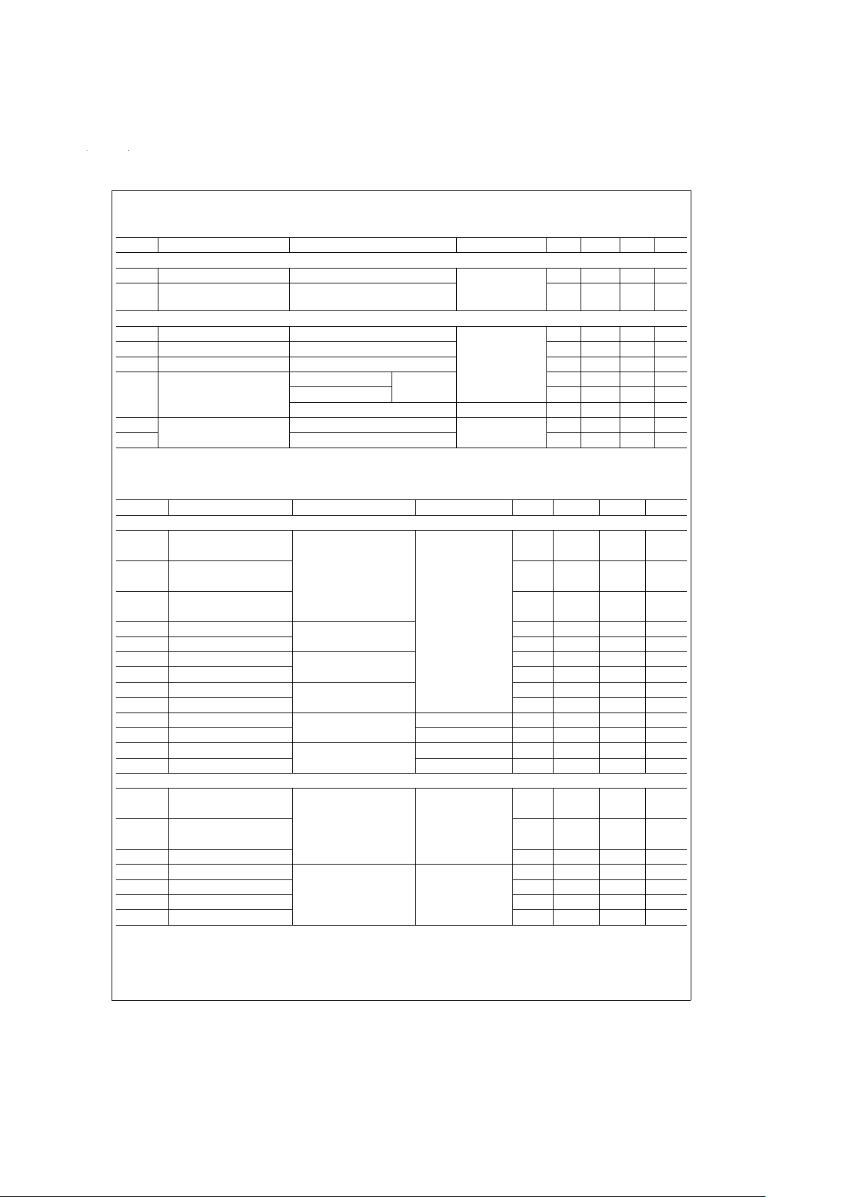
Electrical Characteristics (Notes 3, 4) (Continued)
Over Supply Voltage and Operating Temperature ranges, unless otherwise specified
Symbol Parameter Conditions Reference Min Typ Max Units
RECEIVER CHARACTERISTICS
I
OSR
Short Circuit Current VO= GND RO 7 35 85 mA
I
OZR
TRI-STATE Leakage
Current
VO= 0.4V to 2.4V
±
1µA
DEVICE CHARACTERISTICS
V
IH
High Level Input Voltage
DE/RE*,
DI
2.0 V
CC
V
V
IL
Low Level Input Voltage GND 0.8 V
I
IH
High Level Input Current VIH=V
CC
2µA
I
IL
Low Level Input Current VCC= 5.0V
V
IL
=0V
−2 µA
V
CC
= +3.0V −2 µA
SR=0V SR −1 mA
I
CCR
Power Supply Current
(No Load)
Driver OFF, Receiver ON
V
CC
200 500 µA
I
CCD
Driver ON, Receiver OFF 200 500 µA
Switching Characteristics (Notes 4, 9, 11)
Over Supply Voltage and Operating Temperature ranges, unless otherwise specified
Symbol Parameter Conditions Reference Min Typ Max Units
DRIVER CHARACTERISTICS
t
PHLD
Differential Propagation
Delay High to Low
RL=54Ω,CL= 100 pF
Figures 5, 6
10 399 1000 ns
t
PLHD
Differential Propagation
Delay Low to High
10 400 1000 ns
t
SKD
Differential Skew 0 1 10 ns
|t
PHLD−tPLHD
|
t
r
Rise Time SR = Open 2870 ns
t
f
Fall Time 3070 ns
t
r
Rise Time SR = 100 kΩ 1590 ns
t
f
Fall Time 1640 ns
t
r
Rise Time SR = Short 100 337 1000 ns
t
f
Fall Time 100 348 1000 ns
t
PHZ
Disable Time High to Z CL=15pF
Figures 7, 8
1100 2000 ns
t
PLZ
Disable Time Low to Z
Figures 9, 10
500 800 ns
t
PZH
Enable Time Z to High CL= 100 pF
Figures 7, 8
300 500 ns
t
PZL
Enable Time Z to Low
Figures 9, 10
300 500 ns
RECEIVER CHARACTERISTICS
t
PHL
Propagation Delay
High to Low
CL=15pF
Figures 12, 13
30 210 400 ns
t
PLH
Propagation Delay
Low to High
30 190 400 ns
t
SK
Skew, |t
PHL−tPLH
| 0 20 50 ns
t
PLZ
Output Disable Time CL=15pF
Figures 14, 15, 16
50 150 ns
t
PHZ
55 150 ns
t
PZL
Output Enable Time 40 150 ns
t
PZH
45 150 ns
Note 2: “Absolute Maximum Ratings” are those values beyond which the safety of the device cannot be guaranteed. They are not meant to imply that the devices
should be operated at these limits. The table of “Electrical Characteristics” specifies conditions of device operation.
Note 3: Current into device pins is definedas positive. Current out of device pins is defined as negative. All voltages are referenced to ground except V
OD1
and V
OD2
.
Note 4: All typicals are given for: V
CC
= +5.0V, TA= + 25˚C.
Note 5: Delta |V
OD2
| and Delta |VOC| are changes in magnitude of V
OD2
and VOC, respectively, that occur when input changes state.
www.national.com3
Page 4

Switching Characteristics (Notes 4, 9, 11) (Continued)
Note 6: Threshold parameter limits specified as an algebraic value rather than by magnitude.
Note 7: Hysteresis defined as V
HST=VTH−VTL
.
Note 8: I
IN
includes the receiver input current and driver TRI-STATE leakage current.
Note 9: C
L
includes probe and jig capacitance.
Note 10: For complete details of test, see RS-485.
Note 11: SR = GND for all Switching Characteristics unless otherwise specified.
Parameter Measurement Information
DS012052-2
FIGURE 1. Driver V
OD2
and V
OC
DS012052-18
FIGURE 2. Driver V
OD3
DS012052-3
FIGURE 3. Driver VOHand V
OL
DS012052-4
Vtest = −7V to +12V
FIGURE 4. Driver I
OSD
DS012052-5
FIGURE 5. Driver Differential
Propagation Delay Test Circuit
DS012052-6
FIGURE 6. Driver Differential Propagation Delays
and Differential Rise and Fall Times
DS012052-7
FIGURE 7. TRI-STATE Test Circuit (t
PZH,tPHZ
)
www.national.com 4
Page 5

Parameter Measurement
Information
(Continued)
DS012052-8
FIGURE 8. TRI-STATE Waveforms (t
PZH,tPHZ
)
DS012052-9
FIGURE 9. TRI-STATE Test Circuit (t
PZL,tPLZ
)
DS012052-10
FIGURE 10. TRI-STATE Waveforms (t
PZL,tPLZ
)
DS012052-11
FIGURE 11. Receiver VOHand V
OL
DS012052-12
FIGURE 12. Receiver Differential
Propagation Delay Test Circuit
DS012052-13
FIGURE 13. Receiver Differential Propagation Delay Waveforms
DS012052-14
FIGURE 14. Receiver TRI-STATE Test Circuit
www.national.com5
Page 6

Parameter Measurement Information (Continued)
Typical Application Information
TABLE 1. Device Pin Descriptions
Pin#Name Description
1 RO Receiver Output: When DE/RE* (Receiver Enable) is LOW, the receiver is enabled (ON), if DO/RI ≥
DO*/RI* by 200 mV, RO will be HIGH. If DO/RI ≤ DO*/RI* by 200 mV, RO will be LOW. Additionally RO
will be HIGH for OPEN (Non-terminated) inputs.
2 SR Slew Rate Control: A resistor connected to Ground controls the Driver Output rising and falling edge
rates.
3 DE/RE* Combined Driver and Receiver Output Enable: When signal is LOW the receiver output is enabled and
the driver outputs are in TRI-STATE (OFF). When signaI is HlGH, the receiver output is in TRI-STATE
(OFF) and the driver outputs are enabled.
4 DI Driver Input: When DE/RE* is HlGH, the driver is enabled, if DI is LOW, then DO/RI will be LOW and
DO*/RI* will be HIGH. If DI is HIGH, then DO/RI is HIGH and DO*/RI* is LOW.
DS012052-15
FIGURE 15. Receiver Enable and Disable Waveforms (t
PLZ,tPZL
)
DS012052-16
FIGURE 16. Receiver Enable and Disable Waveforms (t
PHZ,tPZH
)
DS012052-17
FIGURE 17. Typical Pin Connection
www.national.com 6
Page 7

Typical Application Information (Continued)
TABLE 1. Device Pin Descriptions (Continued)
Pin#Name Description
5 GND Ground Connection
6 DO/RI Driver Output/Receiver Input, 485 Bus Pin.
7 DO*/RI* Driver Output/Receiver Input, 485 Bus Pin.
8V
CC
Positive Power Supply Connection: Recommended operating range for VCCis +4.75V to +5.25V.
Unit Load
A unit load for a RS-485 receiver is defined by the input current versus the input voltage curve. The gray shaded region
is the defined operating range from −7V to +12V. The top
border extending from −3V at 0 mA to +12V at +1 mA is defined as one unit load. Likewise, the bottom border extending
from +5V at 0 mA to −7V at −0.8 mA is also defined as one
unit load (see
Figure 18
).A RS-485 driver is capable of driving up to 32 unit loads. This allows upto 32 nodes on a single
bus. Although sufficient for many applications, it is sometime
desirable to have even more nodes. For example an aircraft
that has 32 rows with 4 seats per row could benefit from having 128 nodes on one bus. This would allow signals to be
transferred to and from each individual seat to 1 main station. Usually there is one or two less seats in the last row of
the aircraft near the restrooms and food storage area. This
frees the node for the main station.
The DS36C278, the DS36C279, and the DS36C280 all have
1
⁄2unit load and1⁄4unit load (UL) options available. These
devices will allow upto 64 nodes or 128 nodes guaranteed
over temperature depending upon which option is selected.
The
1
⁄2UL option is available in industrial temperature and
the
1
⁄4UL is available in commercial temperature.
First, for a
1
⁄2UL device the top and bottom borders shown in
Figure 18
are scaled. Both 0 mA reference points at +5V and
−3V stay the same. The other reference points are +12V at
+0.5 mA for the top border and −7V at −0.4 mA for the bottom border (see
Figure 18
). Second, for a1⁄4UL device the
top and bottom borders shown in
Figure 18
are scaled also.
Again, both 0 mA reference points at +5V and −3V stay the
same. The other reference points are +12V at +0.25 mA for
the top border and −7V at −0.2 mA for the bottom border
(see
Figure 18
).
The advantage of the
1
⁄2UL and1⁄4UL devices is the increased number of nodes on one bus. In a single master
multi-slave type of application were the number of slaves exceeds 32, the DS36C278/279/280 may save in the cost of
extra devices like repeaters, extra media like cable, and/or
extra components like resistors.
The DS36C279 and DS36C280 have addition feature which
offer more advantages. The DS36C279 has an automatic
sleep mode function for power conscious applications. The
DS36C280 has a slew rate control for EMI conscious applications. Refer to the sleep mode and slew rate control portion of the application information section in the corresponding datasheet for more information on these features.
Slew Rate Control
The DS36C280 features an adjustable slew rate control.
This feature allows more control over EMl levels than tradition fixed edge rate devices. The slew rate control may be
adjusted with or without any external components. The
DS36C280 offers both low power (I
CC
500 µA max) and low
EMI for an RS-485 interface.
The slew rate control is located at pin two of the device and
only controls the driver output edges. The slew rate control
pin (SR) may be left open or shorted to ground, with or without a resistor. When the SR pin is shorted to ground without
a resistor, the driver output edges will transition typically
350 ns. When the SR pin is left open, the driver output edges
will transition typically 3 µs. When the SR pin is shorted to
ground with a resistor, the driver output edges will transition
between 350 ns and 3 µs depending on the resistor value.
Refer to the slew rate versus resistor value curve in this
datasheet for determining resistor values and expected typical slew rate value. Please note, when slowing the edge
rates of the device (see
Figure 19
) will decrease the maxi-
mum data rate also.
DS012052-19
FIGURE 18. Input Current vs Input Voltage
Operating Range
www.national.com7
Page 8

Slew Rate Control (Continued)
Differential Rise/Fall Time
vs Slew Rate Resistor
DS012052-20
FIGURE 19. Slew Rate Resistor
vs Rise/Fall Time
www.national.com 8
Page 9

Physical Dimensions inches (millimeters) unless otherwise noted
8-Lead (0.150" Wide) Molded Small Outline Package, JEDEC
Order Number DS36C280TM
NS Package Number M08A
8-Lead (0.300" Wide) Molded Dual-In-Line Package
Order Number DS36C280TN
NS Package Number N08E
www.national.com9
Page 10

LIFE SUPPORT POLICY
NATIONAL’S PRODUCTS ARE NOT AUTHORIZED FOR USE AS CRITICAL COMPONENTS IN LIFE SUPPORT DEVICES OR SYSTEMS WITHOUT THE EXPRESS WRITTEN APPROVAL OF THE PRESIDENT OF NATIONAL SEMICONDUCTOR CORPORATION. As used herein:
1. Life support devices or systems are devices or systems which, (a) are intended for surgical implant into
the body, or (b) support or sustain life, and whose failure to perform when properly used in accordance
with instructions for use provided in the labeling, can
be reasonably expected to result in a significant injury
to the user.
2. A critical component is any component of a life support
device or system whose failure to perform can be reasonably expected to cause the failure of the life support
device or system, or to affect its safety or effectiveness.
National Semiconductor
Corporation
Americas
Tel: 1-800-272-9959
Fax: 1-800-737-7018
Email: support@nsc.com
www.national.com
National Semiconductor
Europe
Fax: +49 (0) 1 80-530 85 86
Email: europe.support@nsc.com
Deutsch Tel: +49 (0) 1 80-530 85 85
English Tel: +49 (0) 1 80-532 78 32
Français Tel: +49 (0) 1 80-532 93 58
Italiano Tel: +49 (0) 1 80-534 16 80
National Semiconductor
Asia Pacific Customer
Response Group
Tel: 65-2544466
Fax: 65-2504466
Email: sea.support@nsc.com
National Semiconductor
Japan Ltd.
Tel: 81-3-5639-7560
Fax: 81-3-5639-7507
DS36C280 Slew Rate Controlled CMOS EIA-RS-485 Transceiver
National does not assume any responsibility for use of any circuitry described, no circuit patent licenses are implied and National reserves the right at any time without notice to change said circuitry and specifications.
 Loading...