

Page 1
DS36C200
Dual High Speed Bi-Directional Differential Transceiver
General Description
The DS36C200 is a dual transceiver device optimized for
high data rate and low power applications. This device provides a single chip solution for a dual high speed
bi-directional interface.Also,both control pins may be routed
together for single bit control of datastreams. Both control
pins are adjacent to each other for ease of routing them together. The DS36C200 is compatible with IEEE 1394 physical layer and may be used as an economical solution with
some considerations. Please reference the application information on 1394 for more information. The device is in a
14-lead small outline package. The differential driver outputs
provides low EMI with its low output swings typically 210 mV.
The receiver offers
±
100 mV threshold sensitivity, in addition
to common-mode noise protection.
Features
n Optimized for DSS to DVHS interface link
n Compatible IEEE 1394 signaling voltage levels
n Operates above 100 Mbps
n Bi-directional transceivers
n 14-lead SOIC package
n Ultra low power dissipation
n
±
100 mV receiver sensitivity
n Low differential output swing typical 210 mV
n High impedance during power off
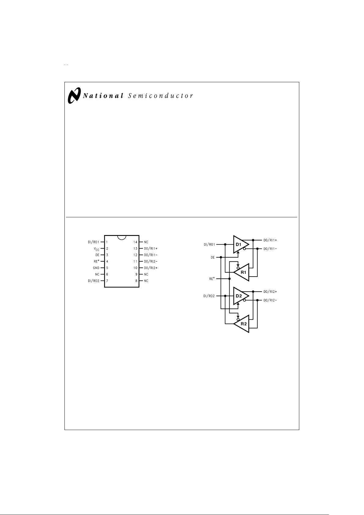
Connection Diagram Functional Diagram
TRI-STATE®is a registered trademark of National Semiconductor Corporation.
DS012621-1
Note:*denotes active LOW pin
Order Number DS36C200M
See NS Package Number M14A
DS012621-2
June 1998
DS36C200 Dual High Speed Bi-Directional Differential Transceiver
© 1998 National Semiconductor Corporation DS012621 www.national.com
Page 2
Absolute Maximum Ratings (Note 1)
If Military/Aerospace specified devices are required,
please contact the National Semiconductor Sales Office/
Distributors for availability and specifications.
Supply Voltage (V
CC
) −0.3V to +6V
Enable Input Voltage
(DE, RE
*
) −0.3V to (VCC+ 0.3V)
Voltage (DI/RO) −0.3V to +5.9V
Voltage (DO/RI
±
) −0.3V to +5.9V
Maximum Package Power Dissipation
@
+25˚C
M Package 1255 mW
Derate M Package 10.04 mW/˚C above +25˚C
Storage Temperature Range −65˚C to +150˚C
Lead Temperature Range
(Soldering, 4 sec.) +260˚C
ESD Rating (Note 4)
(HBM, 1.5 kΩ, 100 pF) ≥ 3.5 kV
(EIAJ, 0 Ω, 200 pF) ≥ 300V
Recommended Operating
Conditions
Min Typ Max Units
Supply Voltage (V
CC
) +4.5 +5.0 +5.5 V
Receiver Input Voltage 0 2.4 V
Operating Free Air
Temperature (T
A
) 0 25 70 ˚C
Electrical Characteristics (Notes 2, 3, 7)
Over supply voltage and operating temperature ranges, unless otherwise specified
Symbol Parameter Conditions Pin Min Typ Max Units
DIFFERENTIAL DRIVER CHARACTERISTICS (RE
*
=
V
CC
)
V
OD
Output Differential Voltage R
L
=
55Ω,(
Figure 1
) DO+,
DO−
172 210 285 mV
∆V
OD
VODMagnitude Change 0 4 35 mV
V
OH
Output High Voltage 1.36 V
V
OL
Output Low Voltage 1.15 V
V
OS
Offset Voltage 1.0 1.25 1.6 V
∆V
OS
Offset Magnitude Change 0 5 25 mV
I
OZD
TRI-STATE®Leakage V
OUT
=
V
CC
or GND −10
±
1 +10 µA
I
OXD
Power-Off Leakage V
OUT
=
5.5V or GND, V
CC
=
0V −10
±
1 +10 µA
I
OSD
Output Short Circuit Current V
OUT
=
0V −4 −9 mA
DIFFERENTIAL RECEIVER CHARACTERISTICS (DE=GND)
V
TH
Input Threshold High V
CM
=
0V to 2.3V RI+,
RI−
+100 mV
V
TL
Input Threshold Low −100 mV
I
IN
Input Current V
IN
=
+2.4V or 0V −10
±
1 +10 µA
V
OH
Output High Voltage I
OH
=
−400 µA RO 3.8 4.9 V
Inputs Open 3.8 4.9 V
Inputs Terminated, R
t
=
55Ω 3.8 4.9 V
Inputs Shorted, V
ID
=
0V 4.9 V
V
OL
Output Low Voltage I
OL
=
2.0 mA, V
ID
=
−200 mV 0.1 0.4 V
I
OSR
Output Short Circuit Current V
OUT
=
0V −15 −60 −100 mA
DEVICE CHARACTERISTICS
V
IH
Input High Voltage DI,
DE
RE
*
2.0 V
CC
V
V
IL
Input Low Voltage GND 0.8 V
I
IH
Input High Current V
IN
=
V
CC
or 2.4V
±
1
±
10 µA
I
IL
Input Low Current V
IN
=
GND or 0.4V
±
1
±
10 µA
V
CL
Input Clamp Voltage I
CL
=
−18 mA −1.5 −0.8 V
I
CCD
Power Supply Current No Load, DE=RE
*
=
V
CC
V
CC
37mA
R
L
=
55Ω,DE=RE
*
=
V
CC
11 17 mA
I
CCR
DE=RE
*
=
0V 6 10 mA
Note 1: “Absolute Maximum Ratings” are those values beyond which the safety of the device cannot be guaranteed. They are not meant to imply that the devices
should be operated at these limits. The table of “Electrical Characteristics” specifies conditions of device operation.
Note 2: Current into device pins is defined as positive. Current out of device pins is defined as negative. All voltages are referenced to ground except V
OD
and VID.
Note 3: All typicals are given for V
CC
=
+5.0V and T
A
=
+25˚C.
Note 4: ESD Rating: HBM (1.5 kΩ, 100 pF) ≥ 3.5 kV
EIAJ (0Ω, 200 pF) ≥ 300V
Note 5: C
L
includes probe and fixture capacitance.
www.national.com 2
Page 3
Electrical Characteristics (Notes 2, 3, 7) (Continued)
Note 6: Generator waveform for all tests unless otherwise specified: f=1 MHz, Z
O
=
50Ω,t
r
≤1 ns, tf≤ 1ns(0%–100%).
Note 7: The DS36C200 is a current mode device and only function with datasheet specification when a resistive load is applied to the drivers outputs.
Switching Characteristic
Over supply voltage and operating temperature ranges, unless otherwise specified. (Notes 5, 6)
Symbol Parameter Conditions Min Typ Max Units
DIFFERENTIAL DRIVER CHARACTERISTICS
t
PHLD
Differential Propagation Delay High to Low R
L
=
55Ω,C
L
=
10 pF
(
Figure 2
and
Figure 3
)
1.0 2.5 5.5 ns
t
PLHD
Differential Propagation Delay Low to High 1.0 2.6 5.5 ns
t
SKD
Differential Skew |t
PHLD–tPLHD
| 0 0.1 2 ns
t
TLH
Transition Time Low to High 0 0.5 2 ns
t
THL
Transition Time High to Low 0 0.5 2 ns
t
PHZ
Disable Time High to Z R
L
=
55Ω
(
Figure 4
and
Figure 5
)
0.3 5 20 ns
t
PLZ
Disable Time Low to Z 0.3 5 20 ns
t
PZH
Enable Time Z to High 0.3 10 30 ns
t
PZL
Enable Time Z to Low 0.3 10 30 ns
DIFFERENTIAL RECEIVER CHARACTERISTICS
t
PHLD
Differential Propagation Delay High to Low C
L
=
10 pF, V
ID
=
200 mV
(
Figure 6
and
Figure 7
)
1.5 5 9 ns
t
PLHD
Differential Propagation Delay Low to High 1.5 4.6 9 ns
t
SKD
Differential Skew |t
PHLD–tPLHD
| 0 0.4 3 ns
t
r
Rise Time 0 1.5 5 ns
t
f
Fall Time 0 1.5 5 ns
t
PHZ
Disable Time High to Z C
L
=
10 pF
(
Figure 8
and
Figure 9
)
1 5 20 ns
t
PLZ
Disable Time Low to Z 1 5 20 ns
t
PZH
Enable Time Z to High 0.3 10 30 ns
t
PZL
Enable Time Z to Low 0.3 10 30 ns
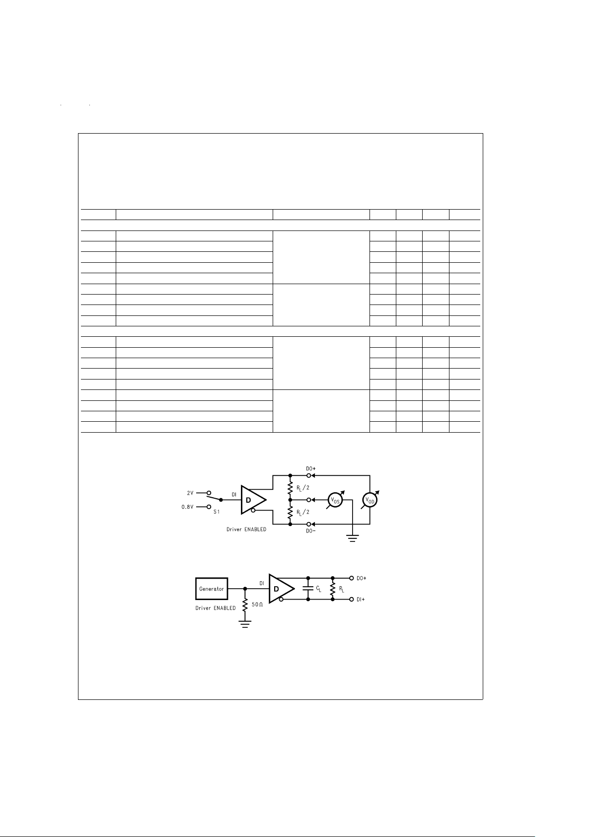
Parameter Measurement Information
DS012621-3
FIGURE 1. Differential Driver DC Test Circuit
DS012621-4
FIGURE 2. Differential Driver Propagation Delay and Transition Time Test Circuit
www.national.com3
Page 4

Parameter Measurement Information (Continued)
DS012621-5
FIGURE 3. Differential Driver Propagation Delay and Transition Time Waveforms
DS012621-6
FIGURE 4. Driver TRI-STATE Delay Test Circuit
DS012621-7
FIGURE 5. Driver TRI-STATE Delay Waveforms
DS012621-8
FIGURE 6. Receiver Propagation Delay and Transition Time Test Circuit
www.national.com 4
Page 5

Parameter Measurement Information (Continued)
Application Information
TRUTH TABLES
The DS36C200 has two enable pins DE and RE
*
, however,
the driver and receiver should never be enabled simultaneously.Enabling both could cause multiple channel contention between the receiver output and the driving logic. It is
recommended to route the enables together on the PC
board. This will allow a single bit [DE/RE
*
] to control the
chip. This DE/RE
*
bit toggles the DS36C200 between Receive mode and Transmit mode. When the bit is asserted
HIGH the device is in Transmit mode. When the bit is asserted LOW the device is in Receive mode. The mode determines the function of the I/O pins: DI/RO, DO/RI+, and
DO/RI−.Please note that some of the pins have been identified by its function in the corresponding mode in the three
tables below.For example, in Transmit mode the DO/RI+ pin
is identified as DO+. This was done for clarity in the tables
only and should not be confused with the pin identification
throughout the rest of this document. Also note that a logic
low on the DE/RE
*
bit corresponds to a logic low on both the
DE pin and the RE
*
pin. Similarly, a logic high on the
DE/RE
*
bit corresponds to a logic high on both the DE pin
and the RE
*
pin.
DS012621-9
FIGURE 7. Receiver Propagation Delay and Transition Time Waveforms
DS012621-10
FIGURE 8. Receiver TRI-STATE Delay Test Circuit
DS012621-11
FIGURE 9. Receiver TRI-STATE Delay Waveforms
www.national.com5
Page 6

Application Information (Continued)
Receive Mode
Input(s) Input/Output
DE RE
*
[RI+] − [RI−] RO
LL
>
+100 mV H
LL
<
−100 mV L
L L 100 mV
>&>
−100 mV X
LH X Z
Transmit Mode
Input(s) Input/Output
DE RE
*
DI DO+ DO−
HH L L H
HHHHL
HH2
>
&
>
0.8 X X
LH X Z Z
H
=
Logic high level
L=Logic low level
X=Indeterminant state
Z=High impedance state
TABLE 1. Device Pin Descriptions
Pin
#
Name Mode Description
(In mode only)
3 DE Transmit Driver Enable: When asserted low driver is disabled. And when
asserted high driver is enabled.
1, 7 DI TTL/CMOS driver input pins
10, 13 DO+ Non-inverting driver output pin
11, 12 DO− Inverting driver output pin
4RE
*
Receive Receiver Enable: When asserted low receiver is enabled. And when
asserted high receiver is disabled.
1, 7 RO Receiver output pin
10, 13 RI+ Positive receiver input pin
11, 12 RI− Negative receiver input pin
5 GND Transmit and Ground pin
2V
CC
Receive Positive power supply pin, +5V±10
%
6, 8, 9, 14 NC No Connect
IEEE 1394
The DS36C200 drives and receives IEEE 1394 physical
layer signal levels. The current mode driver is capable of
driving a 55Ω load with V
OD
between 172 mV and 285 mV.
The DS36C200 is not designed to work with a link layer controller IC requiring full 1394 physical layer compliancy to the
standard. No clock generator, no arbitration, and no encode/
decode logic is provided with this device. For a 1394 link
where speed sensing, bus arbitration, and other functions
are not required, a controller and the DS36C200 will provide
a cost effective, high speed dedicated link. This is shown in
Figure 10
. In applications that require fully compliant 1394
protocol, a link layer controller and physical layer controller
will be required as shown in
Figure 10
. The physical layer
controller supports up to three DC36C200 devices (not
shown).
The DS36C200 drivers are current mode drivers and intended to work with a two 110Ω termination resistors in parallel with each other. The termination resistors should match
the characteristic impedance of the transmission media. The
drivers are current mode devices therefore the resistors are
required. Both resistors are required for half duplex operation and should be placed as close to the DO/RI+ and DO/
RI− pins as possible at opposite ends of the bus. However,if
your application only requires simplex operation, only one
termination resistor is required. In addition, note the voltage
levels will vary from those in the datasheet due to different
loading. Also, AC or unterminated configurations are not
used with this device. Multiple node configurations are pos-
sible as long as transmission line effects are taken into account. Discontinuities are caused by mid-bus stubs, connectors, and devices that affect signal integrity.
The differential line driver is a balanced current source design. A current mode driver, generally speaking has a high
output impedance and supplies a constant current for a
range of loads (a voltage mode driver on the other hand supplies a constant voltage for a range of loads). Current is
switched through the load in one direction to produce a logic
state and in the other direction to produce the other logic
state. The typical output current is mere 3.8 mA, a minimum
of 3.1 mA, and a maximum of 5.2 mA. The current mode re-
quires that a resistive termination be employed to terminate
the signal and to complete the loop as shown in
Figure 11
.
The 3.8 mA loop current will develop a differential voltage of
210 mV across the 55Ω termination resistor which the receiver detects with a 110mV minimum differential noise margin neglecting resistive line losses (driven signal minus receiver threshold (210 mV – 100 mV=110 mV)). The signal
is centered around +1.2V (Driver Offset, V
OS
) with respect to
ground as shown in
Figure 7
.
The current mode driver provides substantial benefits over
voltage mode drivers, such as an RS-422 driver. Its quiescent current remains relatively flat versus switching frequency.Whereas the RS-422 voltage mode driver increases
exponentially in most case between 20 MHz–50 MHz. This
is due to the overlap current that flows between the rails of
the device when the internal gates switch. Whereas the current mode driver switches a fixed current between its output
without any substantial overlap current. This is similar to
www.national.com 6
Page 7

Application Information (Continued)
some ECL and PECL devices, but without the heavy static
I
CC
requirements of the ECL/PECL designs. LVDS requires
>
80%less current than similar PECL devices. AC specifications for the driver are a tenfold improvement over other existing RS-422 drivers.
Fail-safe Feature:
The LVDS receiver is a high gain, high speed device that
amplifies a small differential signal (20mV) to CMOS logic
levels. Due to the high gain and tight threshold of the receiver,care should be taken to prevent noise from appearing
as a valid signal.
The receiver’s internal fail-safe circuitry is designed to
source/sink a small amount of current, providing fail-safe
protection (a stable known state of HIGH output voltage) for
floating, terminated or shorted receiver inputs.
1. Open Input Pins. The DS36C200 is a dual transceiver
device, and if an application requires only one receiver,
the unused channel inputs should be left OPEN. Do not
tie the receiver inputs to ground or any other voltages.
The input is biased by internal high value pull up or pull
down resistors to set the output to a HIGH state. This internal circuitry will guarantee a HIGH, stable output state
for open inputs.
2. Terminated Input. If the driver is disconnected (cable
unplugged), or if the driver is in a TRI-STATE or
power-off condition, the receiver output will again be in a
HIGH state, even with the end of the cable 100Ω termination resistor across the input pins. The unplugged
cable can become a floating antenna which can pick up
noise. If the cable picks up more than 10mV of differential noise, the receiver may see the noise as a valid signal and switch. To insure that any noise is seen as
common-mode and not differential, a balanced interconnect should be used. Twisted pair cable will offer better
balance than flat ribbon cable.
3. Shorted Inputs. If a fault condition occurs that shorts
the receiver inputs together, thus resulting in a 0V differential input voltage, the receiver output will remain in a
HIGH state. Shorted input fail-safe is not supported
across the common-mode range of the device (GND to
2.4V). It is only supported with inputs shorted and no external common-mode voltage applied.
DS012621-14
FIGURE 10. (A) Dedicated IEEE 1394 Link
(B) Full IEEE 1394 Compliant Link
www.national.com7
Page 8

Application Information (Continued)
DS012621-12
FIGURE 11. Typical in Home Application
DS012621-13
FIGURE 12. Typical Interface Connection (Note 7)
www.national.com 8
Page 9

9
Page 10

Physical Dimensions inches (millimeters) unless otherwise noted
LIFE SUPPORT POLICY
NATIONAL’S PRODUCTS ARE NOT AUTHORIZED FOR USE AS CRITICAL COMPONENTS IN LIFE SUPPORT DEVICES OR SYSTEMS WITHOUT THE EXPRESS WRITTEN APPROVAL OF THE PRESIDENT OF NATIONAL SEMICONDUCTOR CORPORATION. As used herein:
1. Life support devices or systems are devices or systems which, (a) are intended for surgical implant into
the body, or (b) support or sustain life, and whose failure to perform when properly used in accordance
with instructions for use provided in the labeling, can
be reasonably expected to result in a significant injury
to the user.
2. A critical component in any component of a life support
device or system whose failure to perform can be reasonably expected to cause the failure of the life support
device or system, or to affect its safety or effectiveness.
National Semiconductor
Corporation
Americas
Tel: 1-800-272-9959
Fax: 1-800-737-7018
Email: support@nsc.com
www.national.com
National Semiconductor
Europe
Fax: +49 (0) 1 80-530 85 86
Email: europe.support@nsc.com
Deutsch Tel: +49 (0) 1 80-530 85 85
English Tel: +49 (0) 1 80-532 78 32
Français Tel: +49 (0) 1 80-532 93 58
Italiano Tel: +49 (0) 1 80-534 16 80
National Semiconductor
Asia Pacific Customer
Response Group
Tel: 65-2544466
Fax: 65-2504466
Email: sea.support@nsc.com
National Semiconductor
Japan Ltd.
Tel: 81-3-5620-6175
Fax: 81-3-5620-6179
14-Lead (0.150" Wide) Molded Small Outline Package, JEDEC
Order Number DS36C200M
NS Package Number M14A
DS36C200 Dual High Speed Bi-Directional Differential Transceiver
National does not assume any responsibility for use of any circuitry described, no circuit patent licenses are implied and National reserves the right at any time without notice to change said circuitry and specifications.
 Loading...