

Page 1
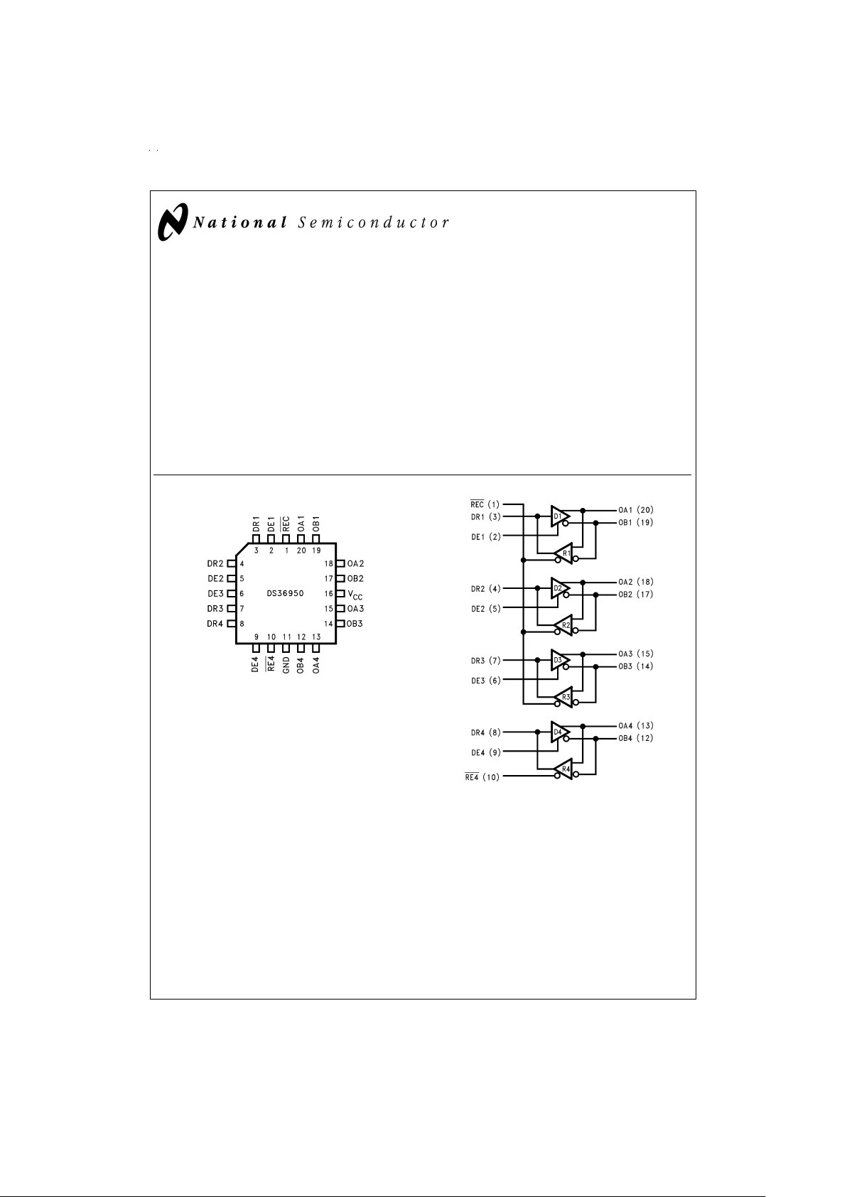
DS36950
Quad Differential Bus Transceiver
General Description
The DS36950 is a low power, space-saving quad EIA-485
differential bus transceiver especially suited for high speed,
parallel, multipoint, computer I/O bus applications. A compact 20-pin surface mount PLCC package provides high
transceiver integration and a very small PC board footprint.
Timing uncertainty across an interface using multiple devices, a typical problem in a parallel interface, is
specified—minimum and maximum propagation delay
times are guaranteed.
Six devices canimplement a complete IPI master or slaveinterface. Three transceivers in a package are pinned out for
connection to a parallel databus. The fourth transceiver, with
the flexibility provided by its individual enables, can serve as
a control bus transceiver.
Features
n Pinout for IPI interface
n Compact 20-pin PLCC package
n Meets EIA-485 standard for multipoint bus transmission
n Greater than 60 mA source/sink
n Thermal Shutdown Protection
Pinout and Logic Diagram
TRI-STATE®is a registered trademark of National Semiconductor Corporation.
DS010602-1
Order Number DS36950
See NS Package Number V20A
DS010602-2
July 1998
DS36950 Quad Differential Bus Transceiver
© 1999 National Semiconductor Corporation DS010602 www.national.com
Page 2
Absolute Maximum Ratings (Note 1)
If Military/Aerospace specified devices are required,
please contact the National Semiconductor Sales Office/
Distributors for availability and specifications.
Supply Voltage 7V
Control Input Voltage V
CC
+ 0.5V
Driver Input Voltage V
CC
+ 0.5V
Driver Output Voltage/Receiver
Input Voltage −10V to +15V
Receiver Output Voltage 5.5V
Continuous Power Dissipation
@
25˚C
V Package 1.73W
Derate V Package 13.9 mW/˚C above 25˚C
Storage Temp. Range −65˚C to +150˚C
Lead Temp. (Soldering 4 Sec.) 260˚C
Recommended Operating
Conditions
Supply Voltage, V
CC
4.75V to 5.25V
Bus Voltage −7V to +12V
Operating Free Air Temp. (T
A
) 0˚C to +70˚C
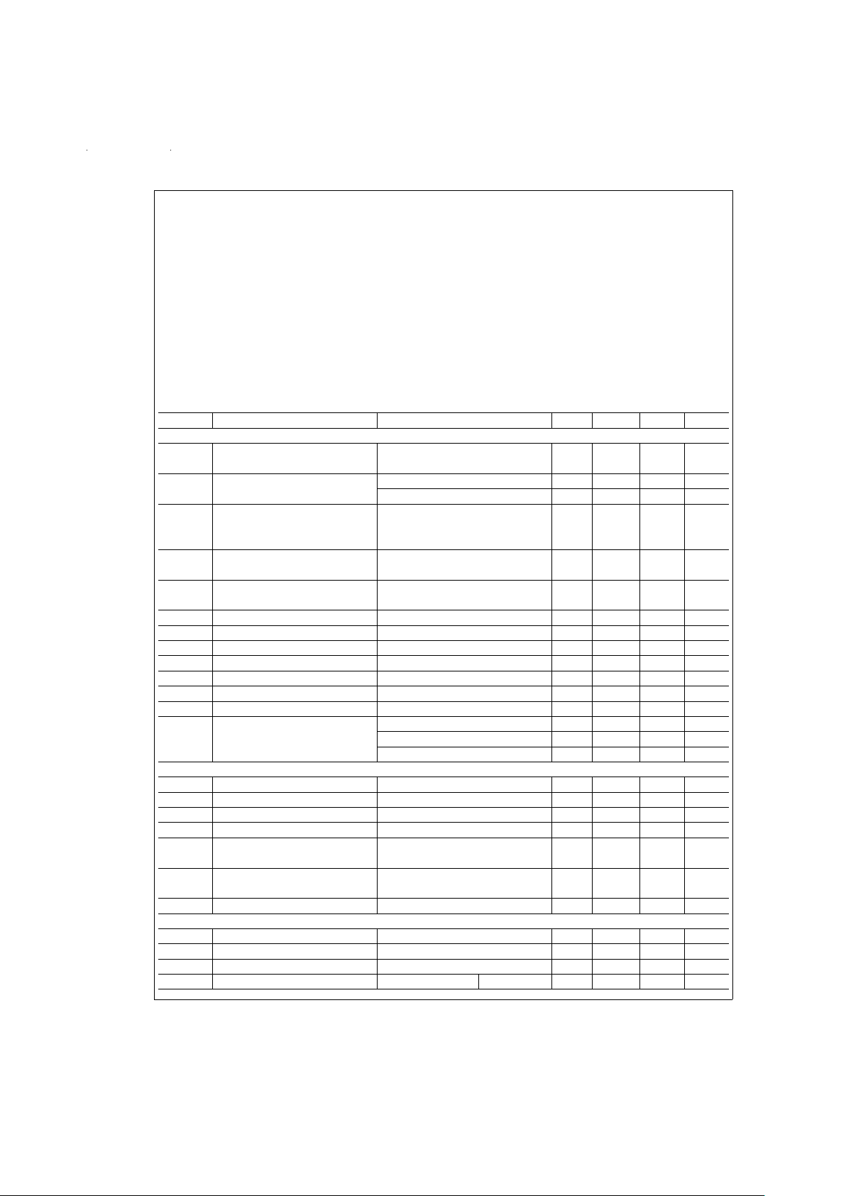
Electrical Characteristics (Note 2)
Over Supply Voltage and Operating Temperature ranges, unless otherwise specified
Symbol Parameter Conditions Min Typ Max Units
DRIVER CHARACTERISTICS
V
ODL
Differential Driver Output I
L
=
60 mA 1.5 1.9 V
Voltage (Full Load) V
CM
=
0V
V
OD
Differential Driver Output R
L
=
100Ω (EIA-422) 2.0 3.5 V
Voltage (Termination Load) R
L
=
54Ω (EIA-485) 1.5 3.2 V
∆IV
OD
I Change in Magnitude of Driver R
L
=
54Ω or 100Ω
Differential Output Voltage for (Note 4) (
Figure 1
) 0.2 V
Complementary Output States (EIA-485)
V
OC
Driver Common Mode Output R
L
=
54Ω 3.0 V
Voltage (Note 5) (
Figure 1
) (EIA-485)
∆IV
OC
I Change in Magnitude of Common (Note 4) (
Figure 1
) 0.2 V
Mode Output Voltage (EIA-485)
V
OH
Output Voltage HIGH I
OH
=
−55 mA 2.7 3.2 V
V
OL
Output Voltage LOW I
OL
=
55 mA 1.4 1.7 V
V
IH
Input Voltage HIGH 2.0 V
V
IL
Input Voltage LOW 0.8 V
V
CL
Input Clamp Voltage I=−18 mA −1.5 V
I
IH
Input High Current V
I
=
2.4V (Note 3) 20 µA
I
IL
Input Low Current V
I
=
0.4V (Note 3) −20 µA
I
OSC
Driver Short-Circuit V
O
=
−7V (EIA-485) −130 −250 mA
Output Current V
O
=
0V (EIA-422) −90 −150 mA
(Note 9) V
O
=
+12V (EIA-485) 130 250 mA
RECEIVER CHARACTERISTICS
I
OSR
Short Circuit Output Current V
O
=
0V (Note 9) −15 −28 −75 mA
I
OZ
TRI-STATE®Output Current V
O
=
0.4V to 2.4V 20 µA
V
OH
Output Voltage High V
ID
=
0.20V, I
OH
=
−0.4 mA 2.4 3.0 V
V
OL
Output Voltage Low V
ID
=
−0.20V, I
OL
=
4 mA 0.35 0.5 V
V
TH
Differential Input High V
O
=
V
OH,IO
=
−0.4 mA 0.03 0.20 V
Threshold Voltage (EIA-422/485)
V
TL
Differential Input Low V
O
=
V
OL,IO
=
4.0 mA −0.20 −0.03 V
Threshold Voltage (Note 6) (EIA-422/485)
V
HST
Hysteresis (Note 7) V
CM
=
0V 35 60 mV
DRIVER AND RECEIVER CHARACTERISTICS
V
IH
Enable Input Voltage High 2.0 V
V
IL
Enable Input Voltage Low 0.8 V
V
CL
Enable Input Clamp Voltage I=−18 mA −1.5 V
I
IN
Line Input Current Other Input=0V V
I
=
+12V 0.5 1 mA
www.national.com 2
Page 3
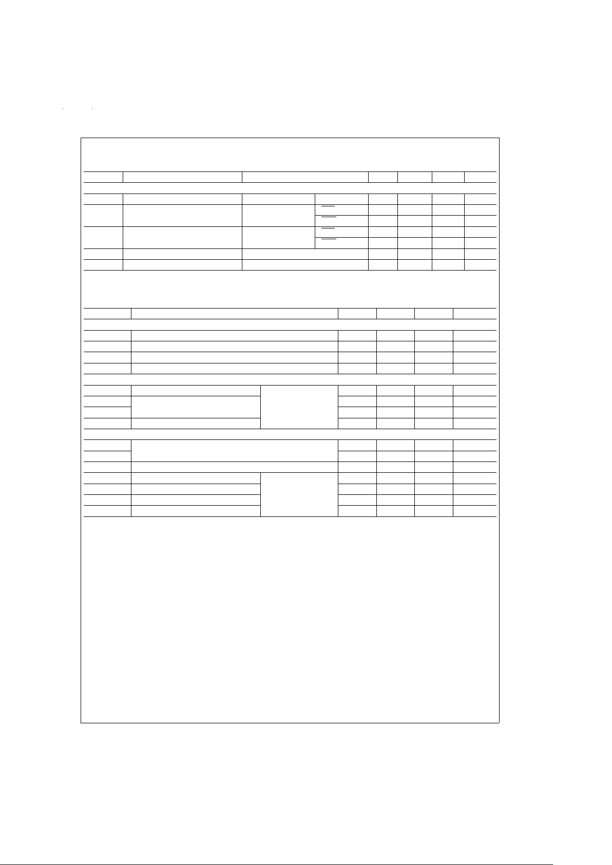
Electrical Characteristics (Note 2) (Continued)
Over Supply Voltage and Operating Temperature ranges, unless otherwise specified
Symbol Parameter Conditions Min Typ Max Units
DRIVER AND RECEIVER CHARACTERISTICS
(Note 8) V
I
=
−7V −0.45 −0.8 mA
I
IH
Enable Input Current High V
OH
=
2.4V RE4 or DE
20 µA
REC
60 µA
I
IL
Enable Input Current Low V
OL
=
0.4V RE4 or DE
−20 µA
REC
−60 µA
I
CC
Supply Current (Note 10) No Load, Outputs Enabled 75 90 mA
I
CCZ
Supply Current (Note 10) No Load, Outputs Disabled 50 70 mA
Switching Characteristics
Over Supply Voltage and Operating Temperature ranges, unless otherwise specified
Symbol Conditions Min Typ Max Units
DRIVER SINGLE-ENDED CHARACTERISTICS
t
PZH
R
L
=
110Ω (
Figure 4
)3540ns
t
PZL
R
L
=
110Ω (
Figure 5
)2540ns
t
PHZ
R
L
=
110Ω (
Figure 4
)1525ns
t
PLZ
R
L
=
110Ω (
Figure 5
)3540ns
DRIVER DIFFERENTIAL CHARACTERISTICS
t
R,tF
Rise & Fall Time R
L
=
54Ω 13 16 ns
t
PLHD
Differential Propagation C
L
=
50 pF 9 15 19 ns
t
PHLD
Delays (Note 15) C
D
=
15 pF 9 15 19 ns
t
SKD
|t
PLHD−tPHLD
| Differential Skew (
Figures 3, 8
)36ns
RECEIVER CHARACTERISTICS
t
PLHD
Differential Propagation Delays 9 14 19 ns
t
PHLD
C
L
=
15 pF, V
CM
=
1.5V (
Figure 6
) 9 14 19 ns
t
SKD
|t
PLHD−tPHLD
| Differential Receiver Skew 1 3 ns
t
ZH
Output Enable Time to High Level 15 22 ns
t
ZL
Output Enable Time to Low Level C
L
=
15 pF 20 30 ns
t
HZ
Output Disable Time from High Level (
Figure 7
)1017ns
t
LZ
Output Disable Time from Low Level 17 25 ns
Note 1: “Absolute Maximum Ratings” are those values beyond which the safety of the device cannot be guaranteed. They are not meant to imply that the devices
should be operated at these limits. The tables of “Electrical Characteristics” specify conditions for device operation.
Note 2: Current into device pins is define as positive. Current out of device pins is defined as negative. All voltages are referenced to ground unless otherwise specified.
Note 3: I
IH
and IILincludes driver input current and receiver TRI-STATE leakage current.
Note 4: ∆IV
OD
I and ∆IVOCI are changes in magnitude of VODand VOC, respectively, that occur when the input changes state.
Note 5: In EIA Standards EIA-422 and EIA-485, V
OC
, which is the average of the two output voltages with respect to ground, is called output offset voltage, VOS.
Note 6: Threshold parameter limits specified as an algebraic value rather than by magnitude.
Note 7: Hysteresis defined as V
HST
=
V
TH−VTL
.
Note 8: I
IN
includes the receiver input current and driver TRI-STATE leakage current.
Note 9: Short one output at a time.
Note 10: Total package supply current.
Note 11: All typicals are given for V
CC
=
5.0V and T
A
=
25˚C.
www.national.com3
Page 4

Parameter Measurement Information
DS010602-3
FIGURE 1. Driver VODand V
OC
DS010602-4
FIGURE 2. Receiver VOHand V
OL
DS010602-5
DS010602-6
FIGURE 3. Driver Differential Propagation Delay and Transition Timing
DS010602-9
S1 to OA for DI=3V
S1 to OB for DI=0V
DS010602-10
FIGURE 4. Driver Enable and Disable Timing (t
PZH,tPHZ
)
DS010602-11
S1 to OA for DI=0V
S1 to OB for DI=3V
DS010602-12
FIGURE 5. Driver Enable and Disable Timing (t
PZL,tPLZ
)
www.national.com 4
Page 5

Parameter Measurement Information (Continued)
DS010602-13
DS010602-14
FIGURE 6. Receiver Differential Propagation Delay Timing
DS010602-15
DS010602-16
S1 1.5V
S2 OPEN
S3 CLOSED
DS010602-17
S1 −1.5V
S2 CLOSED
S3 OPEN
DS010602-18
S1 1.5V
S2 CLOSED
S3 CLOSED
DS010602-19
S1 −1.5V
S2 CLOSED
S3 CLOSED
FIGURE 7. Receiver Enable and Disable Timing
www.national.com5
Page 6

Parameter Measurement Information (Continued)
Note 12: The input pulse is supplied by a generator having the following characteristics:
f=1.0 MHz, 50%Duty Cycle, t
f
and t
r
<
6.0 ns, Z
O
=
50Ω
Note 13: C
L
includes probe and stray capacitance.
Note 14: Diodes are 1N916 or equivalent.
Note 15: Differential propagation delays are calculated from single-ended propagation delays measured from driver input to the 20%and 80%levels on the driver
outputs (See
Figure 8
).
Typical Performance Characteristics
DS010602-20
TCP=Crossing Point
Tra, Trb, Tfa, and Tfb are propagation delay
measurements to the 20%and 80%levels.
FIGURE 8. Propagation Delay Timing for Calculation of Driver Differential Propagation Delays
Driver Differential Propagation
Delay vs Temperature
DS010602-23
Driver Differential Propagation
Delay vs V
CC
DS010602-24
Driver Transition Time
vs Temperature
DS010602-25
Driver Transition Time
vs V
CC
DS010602-27
Driver VOHvs I
OH
vs Temperature
DS010602-26
Driver VOHvs I
OH
vs V
CC
DS010602-28
www.national.com 6
Page 7

Typical Performance Characteristics (Continued)
Driver V
OL
vs I
OL
vs Temperature
DS010602-29
Driver VOLvs I
OL
vs V
CC
DS010602-30
Driver VODvs I
O
vs Temperature
DS010602-31
Driver VODvs I
O
vs V
CC
DS010602-32
Receiver Differential
Propagation Delay
vs Temperature
DS010602-33
Receiver Differential
Propagation
Delay vs V
CC
DS010602-34
Receiver VOHvs I
OH
vs Temperature
DS010602-35
Receiver VOHvs I
OH
vs V
CC
DS010602-36
Receiver VOLvs I
OL
vs Temperature
DS010602-37
www.national.com7
Page 8

Typical Performance Characteristics (Continued)
Receiver V
OL
vs I
OL
vs V
CC
DS010602-38
Supply Current
vs Temperature
DS010602-39
Power Supply Current vs
Power Supply Voltage
DS010602-40
Driver ICCvs Switching
Frequency
DS010602-41
www.national.com 8
Page 9

9
Page 10

Physical Dimensions inches (millimeters) unless otherwise noted
LIFE SUPPORT POLICY
NATIONAL’S PRODUCTS ARE NOT AUTHORIZED FOR USE AS CRITICAL COMPONENTS IN LIFE SUPPORT DEVICES OR SYSTEMS WITHOUT THE EXPRESS WRITTEN APPROVAL OF THE PRESIDENT OF NATIONAL SEMICONDUCTOR CORPORATION. As used herein:
1. Life support devices or systems are devices or systems which, (a) are intended for surgical implant into
the body, or (b) support or sustain life, and whose failure to perform when properly used in accordance
with instructions for use provided in the labeling, can
be reasonably expected to result in a significant injury
to the user.
2. A critical component is any component of a life support
device or system whose failure to perform can be reasonably expected to cause the failure of thelife support
device or system, or to affect its safety or effectiveness.
National Semiconductor
Corporation
Americas
Tel: 1-800-272-9959
Fax: 1-800-737-7018
Email: support@nsc.com
www.national.com
National Semiconductor
Europe
Fax: +49 (0) 1 80-530 85 86
Email: europe.support@nsc.com
Deutsch Tel: +49 (0) 1 80-530 85 85
English Tel: +49 (0) 1 80-532 78 32
Français Tel: +49 (0) 1 80-532 93 58
Italiano Tel: +49 (0) 1 80-534 16 80
National Semiconductor
Asia Pacific Customer
Response Group
Tel: 65-2544466
Fax: 65-2504466
Email: sea.support@nsc.com
National Semiconductor
Japan Ltd.
Tel: 81-3-5639-7560
Fax: 81-3-5639-7507
Order Number DS36950
NS Package Number V20A
DS36950 Quad Differential Bus Transceiver
National does not assume any responsibility for use of any circuitry described, no circuit patent licenses are implied and National reserves the right at any time without notice to change said circuitry and specifications.
 Loading...