

Page 1
DS3669 Quad High Current Peripheral Driver
DS3669 Quad High Current Peripheral Driver
July 1992
General Description
The DS3669 is a non-inverting quad peripheral driver similar
to the DS3658. These drivers are designed for those applications where low operating power, high breakdown voltage, high output current and low output ON voltage are required. A unique input circuit combines TTL compatibility
with high impedance. In fact, its extreme low input current
allows it to be driven directly by a CMOS device.
The outputs are capable of sinking 600 mA each and offer a
70V breakdown. However, for inductive loads the output
should be clamped to 35V or less to avoid latch-up during
turn off (inductive fly back protectionÐrefer AN-213). An onchip clamp diode capable of handling 800 mA is provided at
each output for this purpose. In addition, the DS3669 incorporates circuitry that guarantees glitch-free power up or
down operation.
The molded package is specifically constructed to allow increased power dissipation over conventional packages. The
four ground pins are directly connected to the device chip
with a special copper lead frame. When the quad driver is
soldered into a PC board, the power rating of the device
improves significantly.
Applications
Y
Relay drivers
Y
Lamp drivers
Y
Solenoid drivers
Y
Hammer drivers
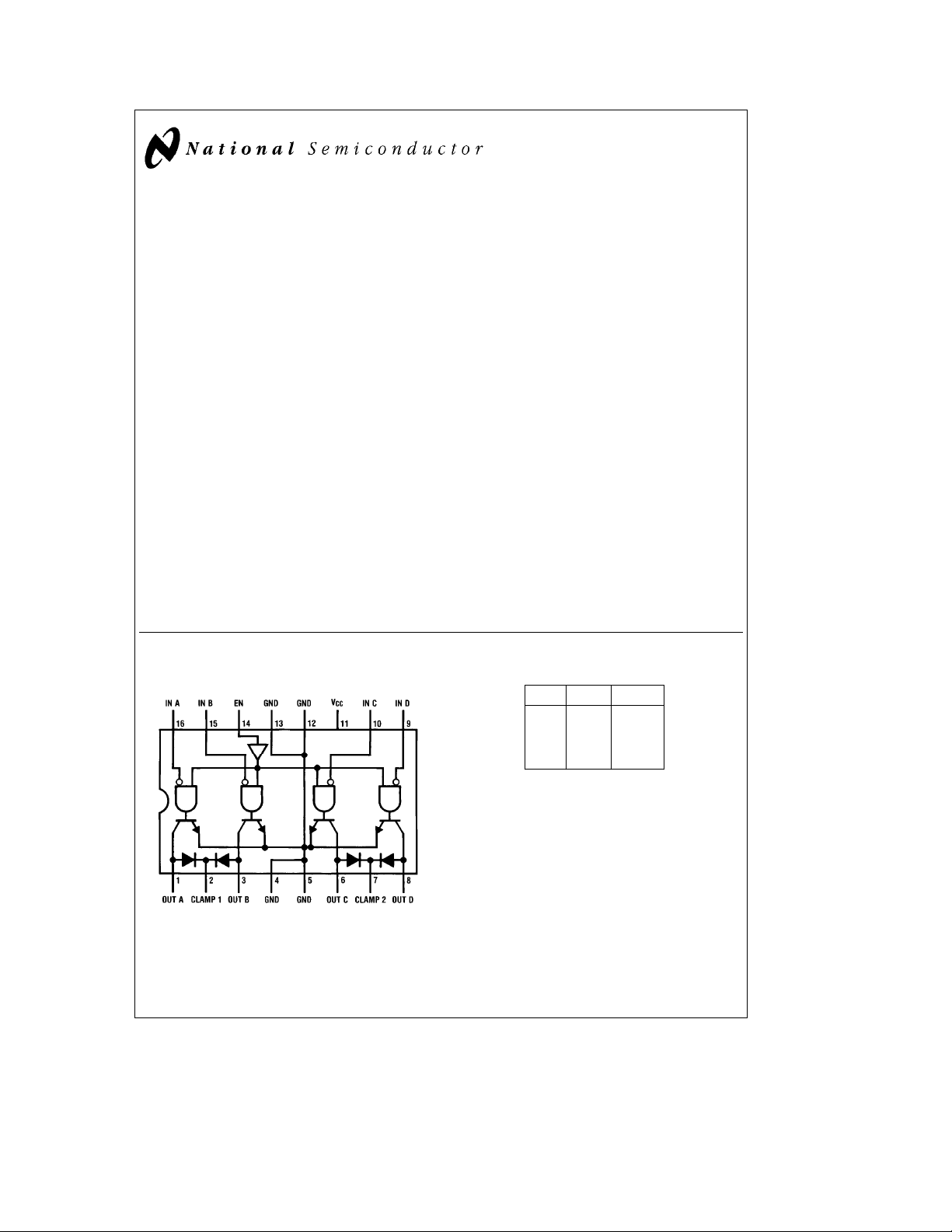
Connection Diagram
Dual-In-Line Package
Y
Stepping motor drivers
Y
Triac drivers
Y
LED drivers
Y
High current, high voltage drivers
Y
Level translators
Y
Fiber optic LED drivers
Features
Y
Single saturated transistor outputs
Y
Low standby power, 10 mW typical
Y
High impedance TTL compatible inputs
Y
Outputs may be tied together for increased current
capacity
Y
High output current
600 mA per output
2.4A per package
Y
No output latch-up at 35V
Y
Low output ON voltage (350 mV typ@600 mA)
Y
High breakdown voltage (70V)
Y
Open collector outputs
Y
Output clamp diodes for inductive fly back protection
Y
NPN inputs for minimal input currents (1 mA typical)
Y
Low operating power
Y
Standard 5V power supply
Y
Power up/down protection
Y
2W power package
Truth Table
IN EN OUT
LH L
HH Z
LL Z
HL Z
e
H
High state
e
L
Low state
e
Z
High impedance state
Top View
TL/F/5820– 1
Order Number DS3669N
See NS Package Number N16E
C
1995 National Semiconductor Corporation RRD-B30M105/Printed in U. S. A.
TL/F/5820
Page 2
Absolute Maximum Ratings (Note 1)
If Military/Aerospace specified devices are required,
please contact the National Semiconductor Sales
Office/Distributors for availability and specifications.
Supply Voltage 7.0V
Input Voltage 15V
Output Voltage 70V
Output Current 1.5A
Continuous Power Dissipation
@
25§C Free-Air (Note 5) 2075 mW
Storage Temperature Range
Lead Temperature (Soldering, 4 seconds) 260§C
Operating Conditions
Min Max Units
Supply Voltage 4.75 5.25 V
Ambient Temperature 0 70
b
65§Ctoa150§C
Electrical Characteristics (Notes 2 and 3)
Symbol Parameter Conditions Min Typ Max Units
V
V
I
IH
I
IL
V
V
I
CEX
V
I
R
I
CC
IH
IL
IK
OL
F
Input High Voltage 2.0 V
Input Low Voltage 0.8 V
Input High Current V
Input Low Current V
Input Clamp Voltage I
Output Low Voltage I
Output Leakage Current V
Diode Forward Voltage I
Diode Leakage Current V
e
5.25V, V
IN
e
0.4V
IN
eb
12 mA
I
e
300 mA 0.2 0.4 V
L
e
I
600 mA (Note 4) 0.35 0.7 V
L
e
70V, V
C
e
V
0.8V
EN
e
800 mA 1.0 1.6 V
F
e
70V 100 mA
R
Supply Current All Inputs Low
e
EN
2.0V
e
5.25V 1.0 10 mA
CC
b
0.8
e
2V,
IN
60 85 mA
g
10 mA
b
1.5 V
100 mA
All Inputs High 2 4 mA
C
§
Switching Characteristics (Note 2)
Symbol Parameter Conditions Min Typ Max Units
t
PHL
t
PLH
Note 1: ‘‘Absolute Maximium Ratings’’ are those values beyond which the safety of the device cannot be guaranteed. They are not meant to imply that the device
should be operated at these limits. The table of ‘‘Electrical Characteristics’’ provides conditions for actual device operation.
Note 2: Unless otherwise specified, min/max limits apply across the 0
values are for T
Note 3: All currents into device pins are shown as positive; all currents out of device pins are shown as negative; all voltages are referenced to ground, unless
otherwise specified. All values shown as max or min are so classified on absolute value basis.
Note 4: All sections of this quad circuit may conduct rated current simultaneously; however, power dissipation averaged over a short interval of time must fall within
specified continuous dissipation ratings.
Note 5: For operation over 25
Turn On Delay R
Turn Off Delay R
e
25§C and V
A
e
5.0V.
CC
C free-air temperature, derate linearly to 1328 mW@70§C@the rate of 16.6 mW/§C.
§
e
L
e
L
e
60X,V
60X,V
30V 226 500 ns
L
e
30V 2430 8000 ns
L
Ctoa70§C temperature range and the 4.75V to 5.25V power supply range. All typical
§
2
Page 3

AC Test Circuit
Switching Waveforms
TL/F/5820– 3
*Includes probe and jig capacitance
Typical Applications
Stepping Motor Driver
*L1, L2, L3, L4 are the windings of a bifilar stepping motor.
**V
is the supply voltage of the motor.
MOTOR
TL/F/5820– 2
TL/F/5820– 4
Lamp Driver
TL/F/5820– 5
3
Page 4

Physical Dimensions inches (millimeters)
DS3669 Quad High Current Peripheral Driver
Molded Dual-In-Line Package (N)
Order Number DS3669N
NS Package Number N16E
LIFE SUPPORT POLICY
NATIONAL’S PRODUCTS ARE NOT AUTHORIZED FOR USE AS CRITICAL COMPONENTS IN LIFE SUPPORT
DEVICES OR SYSTEMS WITHOUT THE EXPRESS WRITTEN APPROVAL OF THE PRESIDENT OF NATIONAL
SEMICONDUCTOR CORPORATION. As used herein:
1. Life support devices or systems are devices or 2. A critical component is any component of a life
systems which, (a) are intended for surgical implant support device or system whose failure to perform can
into the body, or (b) support or sustain life, and whose be reasonably expected to cause the failure of the life
failure to perform, when properly used in accordance support device or system, or to affect its safety or
with instructions for use provided in the labeling, can effectiveness.
be reasonably expected to result in a significant injury
to the user.
National Semiconductor National Semiconductor National Semiconductor National Semiconductor
Corporation Europe Hong Kong Ltd. Japan Ltd.
1111 West Bardin Road Fax: (
Arlington, TX 76017 Email: cnjwge@tevm2.nsc.com Ocean Centre, 5 Canton Rd. Fax: 81-043-299-2408
Tel: 1(800) 272-9959 Deutsch Tel: (
Fax: 1(800) 737-7018 English Tel: (
National does not assume any responsibility for use of any circuitry described, no circuit patent licenses are implied and National reserves the right at any time without notice to change said circuitry and specifications.
Fran3ais Tel: (
Italiano Tel: (
a
49) 0-180-530 85 86 13th Floor, Straight Block, Tel: 81-043-299-2309
a
49) 0-180-530 85 85 Tsimshatsui, Kowloon
a
49) 0-180-532 78 32 Hong Kong
a
49) 0-180-532 93 58 Tel: (852) 2737-1600
a
49) 0-180-534 16 80 Fax: (852) 2736-9960
 Loading...