

Page 1
DS1651/DS3651
Quad High Speed MOS Sense Amplifiers
DS1651/DS3651 Quad High Speed MOS Sense Amplifiers
June 1999
General Description
The DS1651/DS3651 is TTL compatible high speed circuits
intended for sensing in a broad range of MOS memory system applications. Switching speeds have been enhanced
over conventional sense amplifiers by application of Schottky technology, and TRI-STATE
fering a high impedance output state for bused organization.
The DS1651/DS3651 has active pull-up outputs and offers
open collector outputs providing implied “AND” operations.
®
strobing is incorporated, of-
Features
n High speed
n TTL compatible
n Input sensitivity —
n TRI-STATE outputs for high speed buses
n Standard supply voltages —
n Pin and function compatible with MC3430
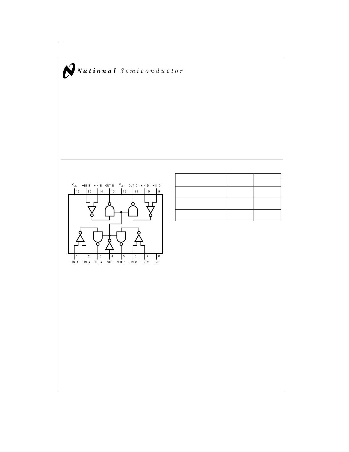
Connection Diagram Truth Table
Dual-in-Line Package
DS007528-1
Top View
Order Number DS1651J, DS3651J or DS3651N
See NS Package Number J16A or N16A
L=Low logic state
H=High logic state
Open=TRI-STATE
X=Indeterminate state
Input Strobe
V
≥ 7mW
ID
= 0˚C to +70˚C
T
A
−7 mV ≤ V
= 0˚C to +70˚C
T
A
V
ID
= 0˚C to +70˚C
T
A
≤ −7 mV
≤ +7 mV
ID
±
7mV
±
5V
Output
DS3651
L
H
L
H
L
H
H
Open
X
Open
L
Open
TRI-STATE®is a registered trademark of National Semiconductor Corporation.
© 1999 National Semiconductor Corporation DS007528 www.national.com
Page 2
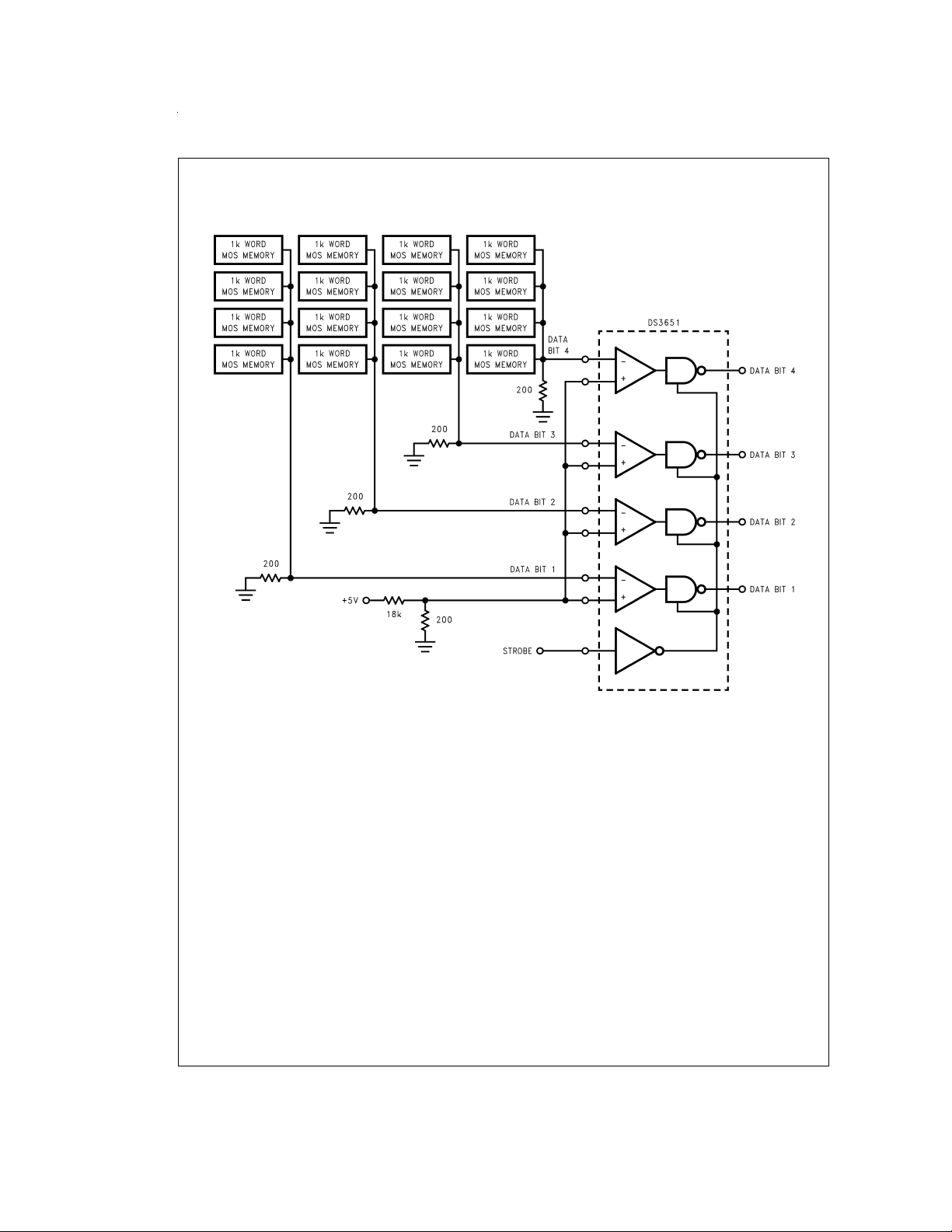
Typical Applications
A Typical MOS Memory Sensing Application for a 4k work by 4-bit
Memory Arrangement Employing 1103 Type Memory Devices
Note: Only 4 devices are required for a 4k word by 16-bit memory system.
www.national.com 2
DS007528-2
Page 3
Absolute Maximum Ratings (Note 2)
If Military/Aerospace specified devices are required,
please contact the National Semiconductor Sales Office/
Distributors for availability and specifications.
Power Supply Voltages
V
CC
V
EE
Differential-Mode Input Signal Voltage
Range, V
Common-Mode Input Voltage Range,
Strobe Input Voltage, V
IDR
V
ICR
I(S)
Strobe Temperature Range −65˚C to +150˚C
Maximum Power Dissipation (Note 1) at 25˚C
Cavity Package
Molded Package
Lead Temp. (Soldering, 10 seconds) 300˚C
+7 V
−7 V
±
6V
±
5V
5.5 V
1509 mW
1476 mW
Operating Conditions
Supply Voltage (V
DS1651
DS3651
Supply Voltage (V
DC
DC
DC
DC
DC
DS1651
DS3651
Operating Temperature (T
DS1651
DS3651
Output Load Current, (I
Differential Mode Input
Voltage Range, (V
Common-Mode Input
Voltage Range, (V
Input Voltage Range
(Any Input to GND), (V
)
Min Max Unit
CC
)
EE
OL
) −5.0 +5.0 V
IDR
) −3.0 +3.0 V
ICR
)
A
4.5
4.75
−4.5
−4.75
−550+125
5.5
5.25
−5.5
−5.25
+70
V
V
V
V
˚C
˚C
)16mA
) −5.0 +3.0 V
IR
Electrical Characteristics
=
V
5V
CC
Symbol Parameter Conditions Min Typ Max Unit
V
IS
V
IO
I
IB
I
IO
V
IL(S)
V
IH(S)
I
IL(S)
I
IL(S)
V
OH
V
OL
I
OS
I
OFF
I
CC
I
EE
=
, Min ≤ TA≤ Max, unless otherwise noted (Notes 3, 4)
DC,VEE
Input Sensitivity (Note 6)
(Common-Mode Voltage
Range)
V
ICR
−5 V
DC
= −3V ≤ VIN≤ +3V
Min ≤ V
Min ≥ V
CC
EE
≤ Max
≥ Max
±
7.0 mV
Input Offset Voltage 2mV
Input Bias Current VCC= Max, VEE= Max 20 µA
Input Offset Current 0.5 µA
Strobe Input Voltage
(Low State)
Strobe Input Voltage
(High State)
2V
0.8 V
Strobe Current (Low State) VCC= Max, VEE= Max, VIN= 0.4V −1.6 mA
Strobe Current (High State) VCC= Max,
= Max
V
EE
Output Voltage (High States) VCC= Min,
= Min
V
EE
Output Voltage (Low State) VCC= Min,
= Min
V
EE
V
= 2.4V DS3651 40 µA
IN
V
IN=VCC
V
= 2.4V DS1651 100 µA
IN
V
IN=VCC
I
= −400 µA DS1651/DS3651
O
=
I
16 mA DS3651 0.45
O
2.4 V
DS1651 0.50
1mA
1mA
V
Output Current Short Circuit VCC= Max, VEE= Max, (Note 5) DS1651/DS3651 −18 −70 mA
Output Disable Leakage
Current
High Logic Level Supply
Current
High Logic Level Supply
Current
VCC= Max, VEE= Max DS3651 40 µA
DS1651 100 µA
VCC= Max, VEE= Max
VCC= Max, VEE= Max
45 60 mA
−17 −30 mA
www.national.com3
Page 4

Switching Characteristics
=
V
5V
CC
Symbol Parameter Conditions Min Typ Max Units
t
PHL(D)
t
PLH(D)
t
POH(S)
t
PHO(S)
t
POL(S)
t
PLO(S)
Note 1: Derate cavity package 10.1 mW/˚C above 25˚C; derate molded package 11.8 mW/˚C above 25˚C.
Note 2: “AbsoluteMaximum Ratings” are those values beyond which the safety of the device cannot be guaranteed. Except for “Operating Temperature Range” they
are not meant to imply that the device should be operated at these limits. The table of “Electrical Characteristics” provides conditions for actual device operation.
Note 3: Unlessotherwise specified min/max limits apply across the 0˚C to +70˚C range for the DS3651 and across the −55˚C to +125˚C range for the DS1651. All
typical values are for T
Note 4: Allcurrents into device pins shown as positive, out of device pins as negative, all voltages referenced to ground unless otherwise noted. All values shown
as max or min on absolute value basis.
Note 5: Only one output at a time should be shorted.
Note 6: Aparameter which is of primary concern when designing with sense amplifiers is, what is the minimum differential input voltage required at the sense am-
plifier input terminals to guarantee a given output logic state. This parameter is commonly referred to as threshold voltage. It is well known that design considerations
of threshold voltage are plagued by input offset currents, bias currents, network source resistances, and voltage gain. As a design convenience, the DS1651 and
DS3651 are specified to a parameter called input sensitivity (V
a minimum input differential voltage to cause a given output logic state with respect to a maximum source impedance of 200Ω at each input.
DC,VEE
=
−5 V
=
25˚C unless otherwise noted.
DC,TA
High-to-Low Logic Level Propagation
Delay Time (Differential Inputs)
Low-to-High Logic Level Propagation
Delay Time (Differential Inputs)
TRI-STATE to High Logic Level
Propagation Delay Time (Strobe)
High Logic Level to TRI-STATE
Propagation Delay Time (Strobe)
TRI-STATE to Low Logic Level
Propagation Delay Time (Strobe)
Low Logic Level to TRI-STATE
Propagation Delay Time (Strobe)
=
A
25˚C, V
CC
=
5V and V
=
EE
5mV+VIS,
Figure 2
(
5mV+VIS,
Figure 2
(
(
Figure 1
(
Figure 1
(
Figure 1
(
Figure 1
−5V.
). This parameter takes into consideration input offset currents and bias currents, and guarantees
IS
DS1651/
)
DS3651
DS1651/
)
DS3651
) DS1651/
DS3651
) DS1651/
DS3651
) DS1651/
DS3651
) DS1651/
DS3651
23 45 ns
22 55 ns
16 21 ns
718ns
19 27 ns
14 29 ns
Switching Time Waveform
Note: Output of channel B shown under test, other channels are tested similarly.
Delay V1 V2 S1 S2 C
t
) 100 mV GND Closed Closed 15 pF
PLO(S)
t
POL(S)
t
PHO(S)
t
POH(S)
CLincludes jig and probe capacitance.
waveform characteristics: t
E
IN
PRR=1 MHz
Duty cycle=50
www.national.com 4
%
100 mV GND Closed Open 50 pF
GND 100 mV Closed Closed 15 pF
GND 100 mV Open Closed 50 pF
TLH
and t
≤ 10 ns measured 10%to 90
THL
%
DS007528-3
L
Page 5

AC Test Circuits
t
PLO(S)
DS007528-4
t
POL(S)
DS007528-6
FIGURE 1. Strobe Propagation Delay t
PLO(S),tPOL(S),tPHL(S)
t
PHO(S)
t
POH(S)
and t
DS007528-5
DS007528-7
POH(S)
Note: Output of channel B shown under test, other channels are tested similarly.
S1 at “B” for DS1651/DS3651, C
EINwaveform characteristics:
and t
t
TLH
PRR=1 MHz, duty cycle=500 ns
≤ 10 ns measured 10%to 90
THL
=
50 pF total for DS1651/DS3651.
L
%
FIGURE 2. Differential Input Propagation Delay t
DS007528-9
PLH(D)
and t
DS007528-8
PHL(D)
www.national.com5
Page 6

Schematic Diagrams
DS1651/DS3651
www.national.com 6
DS007528-10
Page 7

Typical Applications
Level Detector with Hysteresis
DS007528-11
Transfer Characteristics
and Equations for
Level Detector with Hysteresis
DS007528-12
www.national.com7
Page 8

Typical Applications (Continued)
4-Bit Parallel A/D Converter
0
=
2
(A+B)(C+D)(E+F)(H+J)(K+L)(M+N)(P+R)(S)
1
=
2
(B+D)(F+J)(L+N)(R)
2
=
2
(D+J)(N)
3
=
2
J
Conversion time ) 50 ns
www.national.com 8
DS007528-14
Page 9

Physical Dimensions inches (millimeters) unless otherwise noted
Order Number DS1651J, DS1653J, DS3651J or DS3653J
Ceramic Dual-in-Line Package (J)
NS Package Number J16A
Molded Dual-in-Line Package (N)
Order Number DS3651N or DS3653N
NS Package Number N16A
www.national.com9
Page 10

Notes
DS1651/DS3651 Quad High Speed MOS Sense Amplifiers
LIFE SUPPORT POLICY
NATIONAL’S PRODUCTS ARE NOT AUTHORIZED FOR USE AS CRITICAL COMPONENTS IN LIFE SUPPORT
DEVICES OR SYSTEMS WITHOUT THE EXPRESS WRITTEN APPROVAL OF THE PRESIDENT AND GENERAL
COUNSEL OF NATIONAL SEMICONDUCTOR CORPORATION. As used herein:
1. Life support devices or systems are devices or
systems which, (a) are intended for surgical implant
into the body, or (b) support or sustain life, and
whose failure to perform when properly used in
accordance with instructions for use provided in the
labeling, can be reasonably expected to result in a
significant injury to the user.
National Semiconductor
Corporation
Americas
Tel: 1-800-272-9959
Fax: 1-800-737-7018
Email: support@nsc.com
www.national.com
National does not assume any responsibility for use of any circuitry described, no circuit patent licenses are implied and National reserves the right at any time without notice to change said circuitry and specifications.
National Semiconductor
Europe
Fax: +49 (0) 1 80-530 85 86
Email: europe.support@nsc.com
Deutsch Tel: +49 (0) 1 80-530 85 85
English Tel: +49 (0) 1 80-532 78 32
Français Tel: +49 (0) 1 80-532 93 58
Italiano Tel: +49 (0) 1 80-534 16 80
2. A critical component is any component of a life
support device or system whose failure to perform
can be reasonably expected to cause the failure of
the life support device or system, or to affect its
safety or effectiveness.
National Semiconductor
Asia Pacific Customer
Response Group
Tel: 65-2544466
Fax: 65-2504466
Email: sea.support@nsc.com
National Semiconductor
Japan Ltd.
Tel: 81-3-5639-7560
Fax: 81-3-5639-7507
 Loading...