

Page 1
PRELIMINARY
May 9, 2008
DS32EL0421, DS32ELX0421
125 – 312.5 MHz Serializer with DDR LVDS Parallel LVDS
Interface
General Description
The DS32EL0421/DS32ELX0421 is a 125 MHz to 312.5 MHz
(DDR) serializer for high-speed serial transmission over FR-4
printed circuit board backplanes, balanced cables, and optical
fiber. This easy-to-use chipset integrates advanced signal
and clock conditioning functions, with an FPGA friendly interface.
The DS32EL0421/DS32ELX0421 serializes up to 5 parallel
input LVDS channels to create a maximum data payload of
3.125 Gbps. If the integrated DC-balance encoding is enabled, the maximum data payload achievable is 2.5 Gbps.
The DS32EL0421/DS32ELX0421 serializers feature remote
sense capability to automatically detect and negotiate link
status with its companion DS32EL0124/DS32ELX0124 deserializers without requiring an additional feedback path.
The parallel LVDS interface reduces FPGA I/O pins, board
trace count and alleviates EMI issues, when compared to traditional single-ended wide bus interfaces.
The DS32EL0421/DS32ELX0421 is programmable through
a SMBus interface as well as through control pins.
Target Applications
■
Imaging: Industrial, Medical Security, Printers
■
Displays: LED walls, Commercial
■
Video Transport
■
Communication Systems
■
Test and Measurement
■
Industrial Bus
Features
■
5-bit LVDS parallel data interface
■
Programmable transmit de-emphasis
■
Configurable output levels (VOD)
■
Selectable DC-balanced encoder
■
Selectable data scrambler
■
Remote Sense for automatic detection and negotiation of
link status
■
On chip LC VCOs
■
Redundant serial output (ELX device only)
■
Data valid signaling to assist with synchronization of
multiple receivers
■
Supports AC- and DC-coupled signaling
■
Integrated CML and LVDS terminations
■
Configurable PLL loop bandwidth
■
Programmable output termination (50Ω or 75Ω).
■
Built-in test pattern generator
■
Loss of lock and error reporting
■
Configurable via SMBus
■
48-pin LLP package with exposed DAP
Key Specifications
■
1.25 to 3.125 Gbps serial data rate
■
125 to 312.5 MHz DDR parallel clock
■
-40° to +85°C temperature range
■
>8 kV ESD (HBM) protection
■
Low Intrinsic Jitter — 35ps at 3.125 Gbps
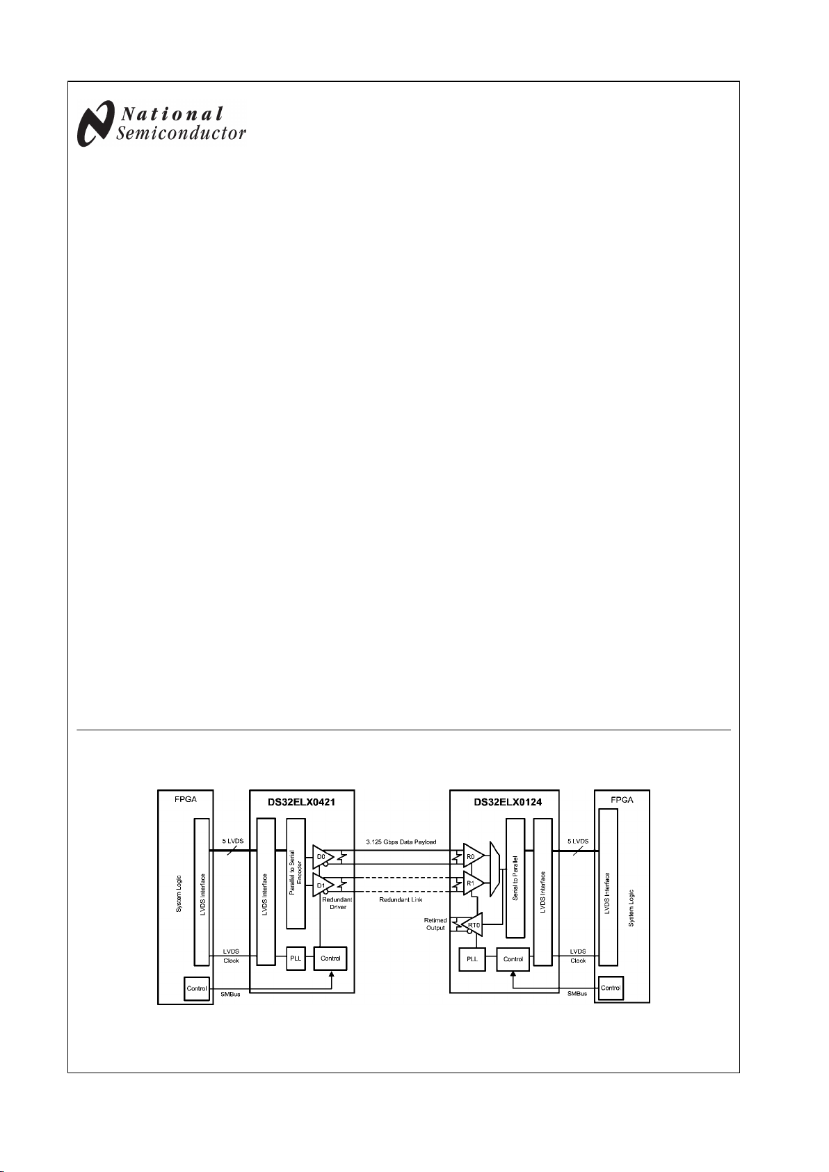
Typical Application
30032101
© 2008 National Semiconductor Corporation 300321 www.national.com
DS32EL0421, DS32ELX0421 125 – 312.5 MHz Serializer with DDR LVDS Parallel LVDS Interface
Page 2
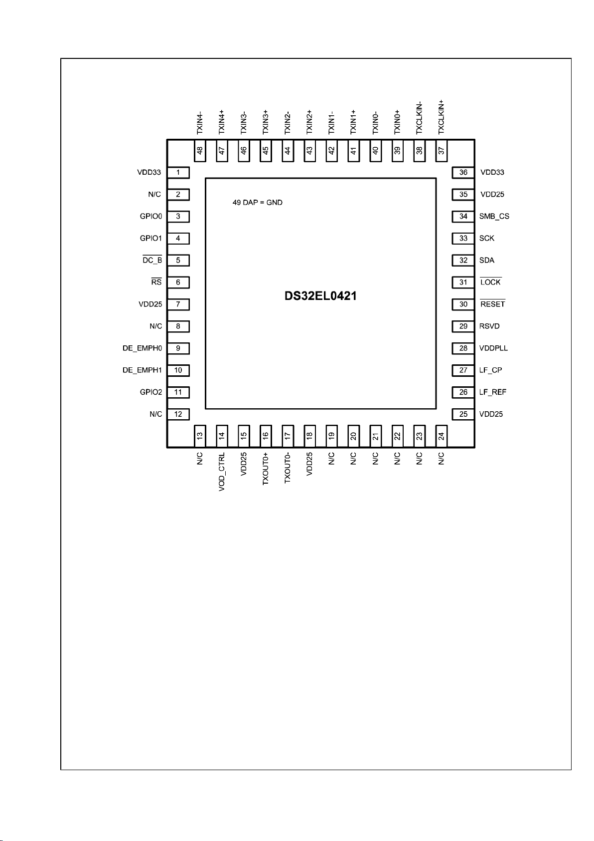
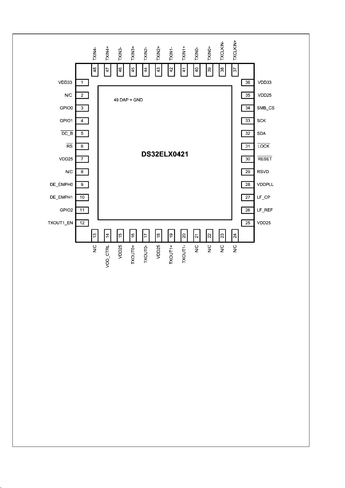
Pin Diagram
30032102
www.national.com 2
DS32EL0421, DS32ELX0421
Page 3
30032103
3 www.national.com
DS32EL0421, DS32ELX0421
Page 4
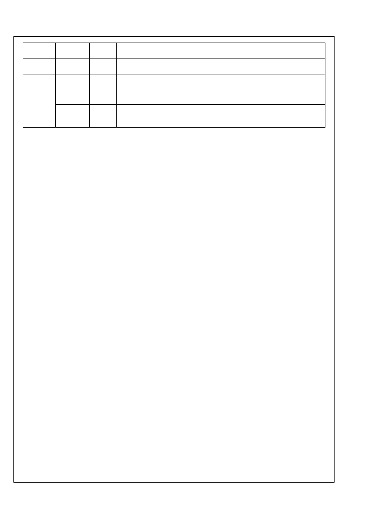
Pin Descriptions
Pin Name Pin Number I/O, Type Description
Power, Ground and Analog Reference
VDD33 1, 36 I, VDD 3.3V supply
VDD25 7, 15, 18, 25,35I, VDD 2.5V supply
VOD_CTRL 14 Analog VOD control. The serializer output amplitude can be adjusted by connecting this pin to a
pull-down resistor. The value of the resistor determines the VOD. Use the following
equation to determine the value of the resistor.
R = (1400 mV / VOD) x 9.1 kΩ
LF_CP 27 Analog Loop filter connection for PLL
LF_REF 28 Analog Loop filter ground reference
Exposed
Pad
49 GND Exposed Pad must be connected to GND by 9 vias
CML I/O
TxOUT0+
TxOUT0-
16
17
O, CML Inverting and non-inverting high speed CML differential outputs of the serializer. These
outputs are internally terminated.
TxOUT1+
TxOUT1-
19
20
O, CML DS32ELX0421 ONLY. Redundancy output. Inverting and non-inverting high speed CML
differential outputs of the serializer. These outputs are internally terminated
LVDS Parallel Data Bus
TxCLKIN+
TxCLKIN-
37
38
I, LVDS Serializer input clock. TxCLKIN+/- are the inverting and non-inverting LVDS transmit
clock input pins.
TxIN[4:0]+/- 39, 40,
41, 42,
43, 44,
45, 46,
47, 48
I, LVDS Serializer input data. TxIN[4:0]+/- are the inverting and non-inverting LVDS serializer
input data pins.
LVCMOS Control Pins
DC_B
RS
5
6
I,
LVCMOS
DC-balance and Remote Sense pins. See Device Configuration section for device
behavior.
DE_EMPH0
DE_EMPH1
9
10
I,
LVCMOS
DE_EMPH0, DE_EMPH1 select the output de-emphasis level. These pins are internally
pull-down.
00: Off
01: Low
10: Medium
11: Maximum
TXOUT1_E
N
12 I,
LVCMOS
DS32ELX0421 ONLY. When held high, redundant output TxOUT1+/- is enabled.
RESET 30 I,
LVCMOS
When held low, reset the device.
0 = Device Reset
1 = Normal operation
LOCK 31 O,
LVCMOS
Lock indication output. The input data on TxIN[0:4]+/- pins is ignored when LOCK pin is
high.
SMBus Interface
SCK 33 I/O,
SMBus
SMBus compatible clock.
SDA 32 I/O,
SMBus
SMBus compatible data line.
SMB_CS 34 I, SMBus SMBus chip select. When held high, SMBus management control is enabled.
Other
GPIO0 3 I/O,
LVCMOS
Software configurable I/O pin.
www.national.com 4
DS32EL0421, DS32ELX0421
Page 5
GPIO1 4 I/O,
LVCMOS
Software configurable I/O pin.
GPIO2 11 I/O,
LVCMOS
Software configurable I/O pin.
NC 2, 8, 12, 13,
19, 20, 21,
22, 23, 24,
29
Misc. No Connect, for DS32EL0421
2, 8, 13, 21,
22, 23, 24,
29
Misc. No Connect, for DS32ELX0421
5 www.national.com
DS32EL0421, DS32ELX0421
Page 6
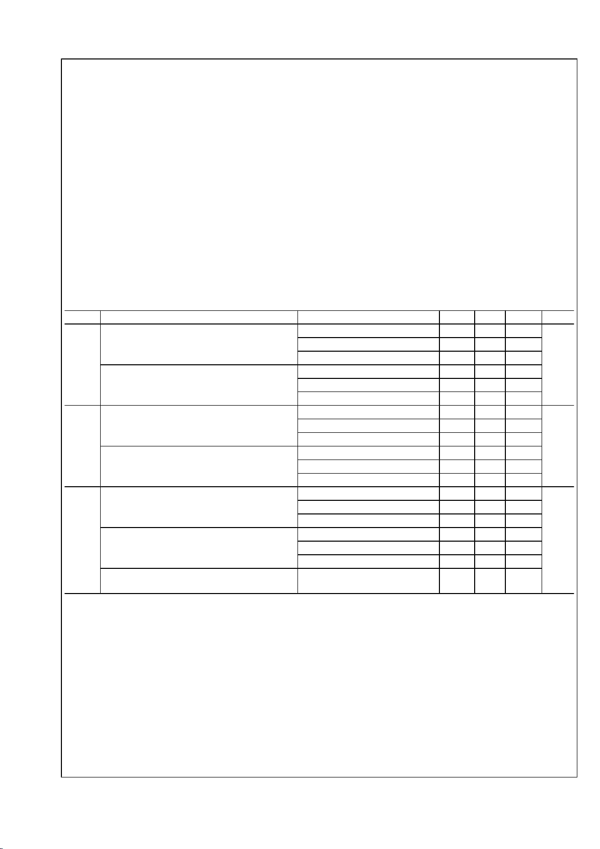
Absolute Maximum Ratings (Note 1)
If Military/Aerospace specified devices are required,
please contact the National Semiconductor Sales Office/
Distributors for availability and specifications.
Supply Voltage (3.3V VDD)
−0.3V to +4V
Supply Voltage (2.5V VDD)
−0.3V to +3V
LVCMOS Input Voltage −0.3V to (VDD + 0.3V)
LVCMOS Output Voltage −0.3V to (VDD + 0.3V)
LVDS Input Voltage (IN+, IN-) −0.3V to +3.6V
CML Output Voltage −0.3V to +3.6V
Junction Temperature +125°C
Storage Temperature Range -65°C to +150°C
Lead Temperature Range
Soldering (4 sec.) +260°C
Thermal Resistance, θ
JA
25°C/W
ESD Susceptibility
HBM (Note 2) >8 kV
Recommended Operating
Conditions
Min Typ Max Units
Supply Voltage (V
DD33
–
GND)
3.135 3.3 3.465 V
Supply Voltage (V
DD25
–
GND)
2.375 2.5 2.625 V
Supply Noise Amplitude
from 10 Hz to 50 MHz
100 mV
P-P
Ambient Temperature (TA) -40 +25 +85 °C
Power Supply Specifications
Symbol Parameter Condition Min Typ Max Unit
I
DD25
2.5V supply current
1 Output Enabled
1.25 Gbps 87 94
mA
2.5 Gbps 95 105
3.125 Gbps 101 112
2.5V supply current
2 Outputs Enabled
1.25 Gbps 126 135
2.5 Gbps 136 145
3.125 Gbps 142 152
I
DD33
3.3V supply current
1 Output Enabled
1.25 Gbps 74 85
mA
2.5 Gbps 74 85
3.125 Gbps 74 85
3.3V supply current
2 Outputs Enabled
1.25 Gbps 80 92
2.5 Gbps 80 92
3.125 Gbps 80 92
P
D
Power Consumption
1 Output Enabled
1.25 Gbps 460 540
mW
2.5 Gbps 485 560
3.125 Gbps 500 575
Power Consumption
2 Output Enabled
1.25 Gbps 580 670
2.5 Gbps 605 695
3.125 Gbps 620 710
Power Consumption
No clock to TxCLKIN
320
www.national.com 6
DS32EL0421, DS32ELX0421
Page 7
Electrical and Timing Characteristics
Over recommended operating supply and temperature ranges unless otherwise specified. (Notes 3, 4, 5)
Symbol Parameter Conditions Min Typ Max Units
LVCMOS ELECTRICAL SPECIFICATIONS
V
IH
High Level Input Voltage 2.0 V
DD
V
V
IL
Low Level Input Voltage 0 0.8 V
V
OH
High Level Output Voltage IOH = -2mA 2.7 3.3 V
V
OL
Low Level Output Voltage IOL = 2mA 0.3 V
V
CL
Input Clamp Voltage ICL = -18mA -0.79 -1.5 V
I
IN
Input Current VIN = 0.4V, 2.5V, or V
DD
-35 35
μA
I
OS
Output Short Circuit Current V
OUT
= 0V
(Note 6)
42 mA
SMBus ELECTRICAL SPECIFICATIONS
V
SIL
Data, Clock Input Low Voltage 0.8 V
V
SIH
Data, Clock Input High Voltage 2 V
SDD
V
I
SPULLUP
Current through pull-up resistor or current source 4 mA
V
SDD
Nominal Bus Voltage 2.375 3.6 V
i
SLEAKB
Input Leakage Per Bus Segment ±200
μA
C
SI
capacitance for SDA and SCLK 10 pF
R
STERM
Termination Resistance V
SDD
= 3.3V 1000
Ω
SMBus TIMING SPECIFICATIONS
t
SMB
Bus Operating Frequency 10 100 kHz
t
BUF
Bus Free Time between Stop and Start Condition 4.7
μs
t
HD:STA
Hold time after (repeated) start condition. After this
period, the first clock is generated.
At I
SPULLUP
= MAX 4.0
μs
t
SU:STA
Repeated Start Condition Setup Time 4.7
μs
t
SU:STO
Stop Condition Setup Time 4.0
μs
t
HD:DAT
Data Hold Time 300 ns
t
SU:DAT
Data Setup Time 250 ns
t
LOW
Clock Low Time 4.7
μs
t
HIGH
Clock High Time 4.0 50
μs
t
F
Clock/Data Fall Time 20% to 80% 300 ns
t
R
Clock/Data Rise Time 1000 ns
t
SU:CS
SMB_CS Setup Time 30 ns
t
POR
Time in which the device must be operation after
power on
500 ms
LVDS ELECTRICAL SPECIFICATIONS
V
TH
Differential Input High Threshold
0.05V < V
LVCM
< V
DD25
– 0.05V
+100 mV
V
TL
Differential Input Low Threshold -100 mV
V
LVCM
LVDS Input Common Mode Voltage 0.05 V
DD25
–
0.05
V
V
LVOS
LVDS Input Loss of Signal LVDS input loss of signal level.
(Note 7)
20 mV
P-P
R
LVIN
Input Impedance Internal LVDS input termination
between differential pairs.
85 100 115
Ω
LVDS TIMING SPECIFICATIONS
f Input DDR Clock (TxCLKIN) Frequency Range 125 312.5 MHz
t
CIP
TxCLKIN Period
See Figure 3
3.2 2T 8 ns
7 www.national.com
DS32EL0421, DS32ELX0421
Page 8
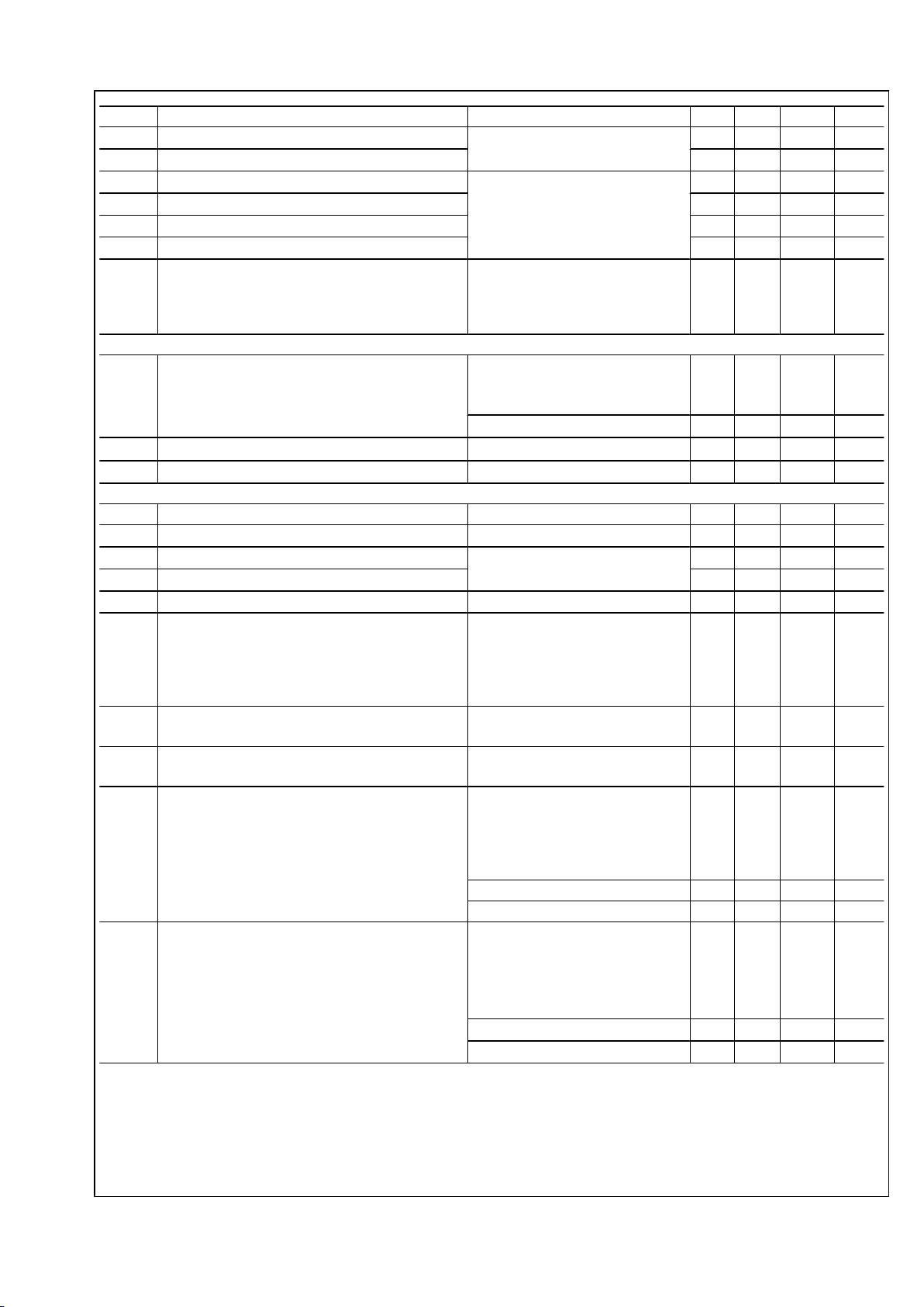
Symbol Parameter Conditions Min Typ Max Units
t
CIT
TxCLKIN Transition Time See Figure 3
(Note 8)
0.5 1.0 3.0 ns
t
XIT
TxIN Transition Time 0.15 3 ns
t
CIH
TxCLKIN High Time See Figure 3 0.7T T 1.3T ns
t
CIL
TxCLKIN Low Time 0.7T T 1.3T ns
t
STC
TxIN Setup to TxCLKIN -550 ps
t
HTC
TxIN Hold to TxCLKIN 900 ps
t
LVDLS
LVDS Input Clock Delay Step Size Programmable through the SMBus,
register 30'h
Default setting = 011'b [7:5]
See Figure 5
100 ps
CML ELECTRICAL SPECIFICATIONS
R
OT
Output Terminations On chip termination from TxOUT0/1
+ and TxOUT0/1 - to V
DD25
50Ω mode
40 50 60
Ω
75Ω mode
60 75 90
Ω
ΔR
OT
Mismatch in Output Termination Resistors 5 %
V
OD
Output Differential Voltage Swing
Based on VOD_CTRL = 9.1 kΩ
1175 1350 1450 mV
P-P
CML TIMING SPECIFICATIONS
LR Line Rate Tested with alternating 1-0 pattern. 1.25 3.125 Gbps
t
OS
Output Overshoot 10 %
t
R
Differential Low to High Transition Time (Note 8) 60 90 ps
t
F
Differential High to Low Transition Time 60 90 ps
t
RFMM
Mismatch in Rise/Fall Time 15 ps
t
DE
De-emphasis width Measured from zero-crossing at
rising edge to 80% of VOD from zerocrossing at falling edge. TDE is
measured at the High setting during
test.
1 UI
t
BIT
Serializer Bit Width 0.2 x
t
CIP
ns
t
SD
Serializer Propagation Delay – Latency t
CIP
+
5.5
ns
t
JIND
Serializer Output Deterministic Jitter Serializer output intrinsic
deterministic jitter. Measure with
PRBS-7 test pattern De-emphasis
disabled.
1.25 Gbps
10
ps
2.5 Gbps 24 ps
3.125 Gbps 21 ps
t
JINR
Serializer Output Random Jitter Serializer output intrinsic random
jitter. Bit error rate ≥10
-15
.
Alternating–10 pattern. De-emphasis
disabled.
1.25 Gbps
1.3
ps
RMS
2.5 Gbps 1.15 ps
RMS
3.125 Gbps 1.14 ps
RMS
www.national.com 8
DS32EL0421, DS32ELX0421
Page 9

Symbol Parameter Conditions Min Typ Max Units
t
JINT
Peak-to-peak Serializer Output Jitter Serializer output peak-to-peak jitter
includes deterministic jitter, random
jitter, and jitter transfer from serializer
input. Measure with PRBS-7 test
pattern. Bit error rate ≥10
-15
. De-
emphasis disabled.
1.25 Gbps
28
ps
2.5 Gbps 38 ps
3.125 Gbps 35 ps
λ
TXBW
Jitter Transfer Function -3 dB Bandwidth 1.25 Gbps
3.125 Gbps
100
300
kHz
kHz
δ
TX
Jitter Transfer Function Peaking 0.5 dB
Note 1: “Absolute Maximum Ratings” indicate limits beyond which damage to the device may occur, including inoperability and degradation of device reliability
and/or performance. Functional operation of the device and/or non-degradation at the Absolute Maximum Ratings or other conditions beyond those indicated in
the Recommended Operating Conditions is not implied. The Recommended Operating Conditions indicate conditions at which the device is functional and the
device should not be operated beyond such conditions.
Note 2: Human Body Model, applicable std. JESD22-A114C
Note 3: The Electrical Characteristics tables list guaranteed specifications under the listed Recommended Operating Conditions except as otherwise modified
or specified by the Electrical Characteristics Conditions and/or Notes. Typical specifications are estimations only and are not guaranteed.
Note 4: Current into device pins is defined as positive. Current out of device pins is defined as negative. All voltages are referenced to ground except VOD and
ΔVOD.
Note 5: Typical values represent most likely parametric norms for VCC = +3.3V and TA = +25°C, and at the Recommended Operation Conditions at the time of
product characterization and are not guaranteed.
Note 6: Output short circuit current (IOS) is specified as magnitude only, minus sign indicates direction only.
Note 7: If input LVDS signal is below 20mV
P-P
, loss of signal (LOS) is detected. The device will flag a valid input signal if the signal level is above 100mV
P-P
Note 8: Specification guaranteed by characterization.
9 www.national.com
DS32EL0421, DS32ELX0421
Page 10

Timing Diagrams
30032106
FIGURE 1. SMBus timing parameters
30032111
FIGURE 2. Serializer Input Clock Transition Time
30032110
FIGURE 3. Serializer (LVDS Interface) Setup/Hold and High/Low Times
www.national.com 10
DS32EL0421, DS32ELX0421
Page 11

30032113
FIGURE 4. LVDS Input Clock Delay
30032112
FIGURE 5. Propagation Delay Timing Diagram
30032104
FIGURE 6. 5-Bit Parallel LVDS Inputs Mapped to CML Output
11 www.national.com
DS32EL0421, DS32ELX0421
Page 12

Functional Description
POWER SUPPLIES
The DS32EL0421 and DS32ELX0421 have several power
supply pins, at 2.5V as well as 3.3V. It is important that these
pins all be connected and properly bypassed. Bypassing
should consist of parallel 4.7μF and 0.1μF capacitors as a
minimum, with a 0.1μF capacitor on each power pin. A 22 μF
capacitor is required on the VDDPLL pin which is connected
to the 3.3V rail.
These devices have a large contact in the center on the bottom of the package. This contact must be connected to the
system GND as it is the major ground connection for the device.
POWER UP
It is recommended, although not necessary, to bring up the
3.3V power supply before the 2.5V supply. If the 2.5V supply
is powered up first, an initial current draw of approximately
600mA from the 2.5V rail may occur before settling to its final
value. Regardless of the sequence, both power rails should
monotonically ramp up to their final values.
POWER MANAGEMENT
These devices have two methods to reduce power consumption. To enter the first power save mode, the on board host
FPGA or controlling device can cease to output the DDR
transmit clock. To further reduce power consumption, write
40'h to register 26'h and 10'h to register 01'h. This will put the
device in its lowest power consumption mode.
RESET
There are three ways to reset these devices. A reset occurs
automatically during power-up. The device can also be reset
by pulling the RESET pin low, with normal operation resuming
when the pin is driven high again. The device can also be
reset by writing to the reset register. This reset will put all of
the register values back to their default values, except it will
not affect the address register value if the SMBus default address has been changed.
LVDS INPUTS
The DS32EL0421 and DS32ELX0421 have standard 2.5V
LVDS inputs which are compliant with ANSI/TIA/EIA-644.
These inputs have internal 100Ω termination resistors. It is
recommended that the PCB trace between the FPGA and the
serializer be less than 40-inches. Longer PCB traces may
degrade the quality of the input signal. The connection between the host and the DS32EL0421 or DS32ELX0421
should be over a controlled impedance transmission line with
impedance that matches the termination resistor – usually
100Ω. Setup and hold times are specified in the LVDS Switch-
ing Characteristics table, however the clock delay can be
adjusted by writing to register 30’h.
LOOP FILTER
The DS32EL0421 and DS32ELX0421 have an internal PLL
which is used to generate the serialization clock from the parallel clock input. The loop filter for this PLL is external; and for
optimum results, a 100nF capacitor and a 1.5 kΩ resistor in
series should be connected between pins 26 and 27. See
typical interface circuit (Figure 11).
REMOTE SENSE
The remote sense feature can be used when a DS32EL0421
or DS32ELX0421 serializer is directly connected to a
DS32EL0124 or DS32ELX0124 deserializer. Active components in the signal path between the serializer and the deserializer may interfere with the back channel signaling of the
devices.
When remote sense is enabled, the serializer will cycle
through four states to successfully establish a link and align
the data. The state diagram for the serializer is shown in Fig-
ure 7. The serializer will remain in the low power IDLE state
until it receives an input clock. Once the PLL of the serializer
has locked to the input clock, the device will enter the LINK
DETECT state. While in this state, the serializer will monitor
the line to see if the deserializer is present. If a deserializer is
detected, the serializer will enter the LINK ACQUISITION
state. The serializer will transmit the entire training pattern
and then enter the NORMAL state. If the deserializer is unable
to successfully lock or maintain lock, it will break the link
sending the serializer back to the IDLE or LINK DETECT
states.
DC-BALANCE ENCODER
The DS32EL0421 and DS32ELX0421 have a built-in DC-balance encoder to support AC-coupled applications. When enabled, the input signal on TXIN4+/- is treated as a data valid
bit. If TXIN4+/- is low, then the four bit nibbles from TXIN0TXIN3 are taken to form a 16 bit word. This 16 bit word is
processed as two 8 bit words and converted to two 10 bit
words by using the standard 8b/10b data coding scheme. The
two 10 bit words are then combined to create a 20 bit code.
This 20 bit word is serialized and driven on the output. The
nibble taken in on the rising edge of the clock is the most significant nibble and the nibble taken in on the falling edge is
the least significant nibble. If TXIN4+/TXIN4- is high, then the
inputs TXIN0 -TXIN3 are ignored and a programmable DCbalanced character is inserted in the output stream. The
default character is a K28.5 code. In order to send other K
codes, they must first be programmed into the serializer via
the SMBus.
www.national.com 12
DS32EL0421, DS32ELX0421
Page 13

30032115
FIGURE 7. Serializer State Diagram
SCRAMBLER
If the scrambler is enabled, the raw or DC-balanced serialized
data is scrambled to improve transition density. The scrambler accepts 20 bits of data and encodes it using the polynomial X9 + X4 + 1. The data can then be sent to the NRZ-toNRZI converter before being output. Data is converted ot teh
NRZI format using the polynomial X + 1.
Enabling the scrambler helps to lower EMI emissions by
spreading the spectrum of the data. Scrambling also creates
transitions for the deserializer’s CDR to properly lock onto.
The scrambler and NRZI encoder are enabled or disabled by
default depending on how the DC_B
and RS pins are configured. To override the default scrambler setting two register
writes must be performed. First, write to register 22’h and set
bit 3 to unlock the scrambler register. Next write to register
21’h and change bit 4 to the desired value. The NRZI encoder
can be enabled or disabled independently of the scrambler by
controlling bit 7 of register 21'h and bit 4 of register 22'h.
CML OUTPUT DATA INTERFACING
The serial outputs provide low-skew differential signals. Internal resistors connected from TxOUTn+ and TxOUTn- to
VDD25 terminate the outputs. The output level can be programmed by adjusting the pull-down resistor to the
VOD_CTRL pin. The output terminations can also be programmed to be either 50 Ω or 75 Ω.
The output buffer consists of a current mode logic (CML) driver with user configurable de-emphasis control, which can be
used to optimize performance over a wide range of transmission line lengths and attenuation distortions resulting from low
cost CAT(-5, -6, -7) cable or FR–4 backplane. Output de-emphasis is user programmable through either device pins
DE_EMPH0 and DE_EMPH1 or SMBus interface. Users can
control the strength of the de-emphasis to optimize for a specific system environment. Please see the De-Emphasis Control Table for details.
De-Emphasis Control Table
DE_EMPH[1:0] Output De-Emphasis Level
00'b Off
01'b Low
10'b Medium
11'b High
The DS32ELX0421 provides a secondary serial output, supporting redundancy applications. The redundant output driver
can be enabled by setting TXOUT1_EN pin to HIGH or by
activating it through the SMBus reigsters.
DEVICE CONFIGURATION
There are four ways to configure the DS32EL0421 and
DS32ELX0421 serializers, these combinations are shown in
Table 1. Depending on which features are enabled, the serializers operate in very different ways. The Remote Sense and
DC-Balance pins are active low configuration pins. The
scrambler and NRZI encoder can be enabled or disabled
through register programming.
When Remote Sense is enabled, with RS pin tied low, the
serializer must be connected directly to a DS32EL0124 or
DS32ELX0124 deserializer without any active components
between them. The Remote Sense module features both an
upstream and downstream communication method for the
serializer and deserializer to communicate. This feature is
used to pass link status information between the 2 devices.
13 www.national.com
DS32EL0421, DS32ELX0421
Page 14

If DC-Balance is enabled, a maximum of 4 parallel LVDS
lanes can be used to receive data. The fifth lane (TXIN4±) is
used for Data Valid signaling. Each time a serializer establishes a link to a deserializer with DC-Balance enabled, the
Data Valid input to the serializer must be held high for 20
LVDS clock periods. If the Data Valid input to the serializer is
logic HIGH, then SYNC characters are transmitted. If the deserializer receives a SYNC character, then the LVDS data
outputs will all be logic low and the Data Valid output will be
logic high. If the deserializer detects a DC-Balance code error,
the output data pins will be set to logic high with the Data Valid
output also set to logic high.
In the case where DC-Balance is enabled and Remote Sense
is disabled, with RS set to high and DC_B set to low, an ex-
ternal device must toggle the Data Valid input to the serializer
periodically to ensure constant lock. With these pin settings
the DS32EL0421/DS32ELX0421 and DS32EL0124/
DS32ELX0124 devices can interface with other active component in the high speed signal path, such as fiber modules.
When both Remote Sense and DC-Balance are disabled,
RS and DC_B pins set to high, the data is not aligned. In this
configuration, data formatting is handled by an FPGA or external source. This pin setting combination also allows for the
DS32EL0421/DS32ELX0421 and DS32EL0124/
DS32ELX0124 devices to nterface with other active components in the high speed signal path.
TABLE 1. Device Configuration Table
Remote Sense Pin (RS) DC-Balance Pin (DC_B) Configuration
0 0 Remote Sense enabled
DC-Balance enabled
Data Alignment
Scrambler and NRZI encoder disabled by default
0 1 Remote Sense enabled
DC-Balance disabled
Data Alignment
Scrambler and NRZI encoder enabled by default
1 0 Remote Sense disabled
DC-Balance enabled
Data Alignment
Scrambler and NRZI encoder enabled by default
1 1 Remote Sense disabled
DC-Balance disabled
No Data Alignment
Scrambler and NRZI encoder disabled by default
www.national.com 14
DS32EL0421, DS32ELX0421
Page 15

SMBus INTERFACE
The System Management Bus interface is compatible to SMBus 2.0 physical layer specification. The use of the Chip
Select signal is required. Holding the SMB_CS pin HIGH enables the SMBus port, allowing access to the configuration
registers. Holding the SMB_CS pin LOW disables the
device's SMBus, allowing communication from the host to
other slave devices on the bus. In the STANDBY state, the
System Management Bus remains active. When communication to other devices on the SMBus is active, the SMB_CS
signal for the serializer must be driven LOW.
The address byte for all DS32EL0421 and DS32ELX0421
devices is AE'h. Based on the SMBus 2.0 specification, these
devices have a 7-bit slave address of 1010111'b. The LSB is
set to 0'b (for a WRITE), thus the 8-bit value is 1010 1110 'b
or AE'h.
The SCK and SDA pins are 3.3V LVCMOS signaling and include high-Z internal pull up resistors. External low
impedance pull up resistors maybe required depending upon
SMBus loading and speed. Note, these pins are not 5V tolerant.
Transfer of Data via the SMBus
During normal operation the data on SDA must be stable during the time when SCK is HIGH.
There are three unique states for the SMBus:
START A HIGH to LOW transition on SDA while SCK is
HIGH indicates a message START condition
STOP A LOW to HIGH transition on SDA while SCK is
HIGH indicates a message STOP condition.
IDLE If SCK and SDA are both high for a time exceeding
t
BUF
from the last detected STOP condition or if they
are HIGH for a total exceeding the maximum
specification for t
HIGH
then the bus will transfer to
the IDLE state.
SMBus Transactions
The devices support WRITE and READ transactions. See
Register Description Table for register address, type (Read/
Write, Read Only), default value and function information.
Writing to a Register
To write a register, the following protocol is used (see SMBus
2.0 specification).
1.
The Host (Master) selects the device by driving its
SMBus Chip Select (SMB_CS) signal HIGH.
2.
The Host drives a START condition, the 7-bit SMBus
address, and a “0” indicating a WRITE.
3.
The Device (Slave) drives the ACK bit (“0”).
4.
The Host drives the 8-bit Register Address.
5.
The Device drives an ACK bit (“0”).
6.
The Host drive the 8-bit data byte.
7.
The Device drives an ACK bit (“0”).
8.
The Host drives a STOP condition.
9.
The Host de-selects the device by driving its SMBus CS
signal Low.
The WRITE transaction is completed, the bus goes IDLE and
communication with other SMBus devices may now occur.
Reading a Register
To read a register, the following protocol is used (see SMBus
2.0 specification).
1.
The Host (Master) selects the device by driving its
SMBus Chip Select (SMB_CS) signal HIGH.
2.
The Host drives a START condition, the 7-bit SMBus
address, and a “0” indicating a WRITE.
3.
The Device (Slave) drives the ACK bit (“0”).
4.
The Host drives the 8-bit Register Address.
5.
The Device drives an ACK bit (“0”).
6.
The Host drives a START condition.
7.
The Host drives the 7-bit SMBus Address, and a “1”
indicating a READ.
8.
The Device drives an ACK bit “0”.
9.
The Device drives the 8-bit data value (register contents).
10.
The Host drives a NACK bit “1”indicating end of the
READ transfer.
11.
The Host drives a STOP condition.
12.
The Host de-selects the device by driving its SMBus CS
signal Low.
The READ transaction is completed, the bus goes IDLE and
communication with other SMBus devices may now occur.
SMBus Configurations
Many different configurations of the SMBus are possible and
depend upon the specific requirements of the applications.
Several possible applications are described.
Configuration 1
The deserializer SMB_CS may be tied High (always enabled)
since it is the only device on the SMBus. See Figure 8.
Configuration 2
Since the multiple SER devices have the same address, the
use of the individual SMB_CS signals is required. To communicate with a specific device, its SMB_CS is driven High to
select the device. After the transaction is complete, its
SMB_CS is driven Low to disable its SMB interface. Other
devices on the bus may now be selected with their respective
chip select signals and communicated with. See Figure 9.
Configuration 3
The addressing field is limited to 7-bits by the SMBus protocol.
Thus it is possible that multiple devices may share the same
7-bit address. An optional feature in the SMBus 2.0 specification supports an Address Resolution Protocol (ARP). This
optional feature is not supported by the DS32EL0421/
DS32ELX0421 devices. Solutions for this include: the use of
the independent SMB_CS signals, independent SMBus segments, or other means.
15 www.national.com
DS32EL0421, DS32ELX0421
Page 16

30032107
FIGURE 8. SMBus Configuration 1
30032108
FIGURE 9. SMBus Configuration 2
30032109
FIGURE 10. SMBus Daisy Chained CS Configuration
www.national.com 16
DS32EL0421, DS32ELX0421
Page 17

Applications Information
GPIO PINS
The GPIO pins can be useful tools when debugging or evaluating the system. For specific GPIO configurations and functions refer to registers 2, 3, 4, 5 and 6 in the device register
map.
GPIO pins are commonly used when there are multiple serializers on the same SMBus. In order to program individual
settings into each serializer, they will each need to have a
unique SMBus address. To reprogram multiple serializers on
a single SMBus, configure the first serializer such that the
SMBus lines are connected to the FPGA or host controller.
The CS pin of the second serializer should be tied to GPIO0
of the first serializer, with the CS pin of the next seriazlier tied
to GPIO0 of its preceding serializer. By holding all of the
GPIO0 pins low, the first serializer’s address may now be reprogrammed by writing to register 0. The first serializer’s
GPIO pin can now be asserted and the second serializer’s
address may now be reprogrammed.
HIGH SPEED COMMUNICATION MEDIA
Using the serializer’s integrated de-emphasis blocks in combination with the DS32EL0124 or DS32ELX0124’s integrated
equalization blocks allows data to be transmitted across a
variety of media at high speeds. Factors that can limit device
performance include excessive input clock jitter, noisy power
rails, EMI from nearby noisy components and poor layout
techniques. Although many cables contain wires of similar
gauge and shielding, performance can vary greatly depending on the quality of the connector.
REDUNDANCY APPLICATIONS
The DS32ELX0421 has two high speed CML serial outputs.
SMBus register control allows the device to use a single output exclusively, or both outputs simultaneously. This allows a
single serializer to transmit data to two independant receiving
systems, a primary and secondary endpoint. Some applications require a redundancy measure in case the primary
signal path is compromised. The secondary output can be
activated “on-the-go”, if a problem is detected on the primary
link.
LINK AGGREGATION
Multiple DS32EL0421/DS32ELX0421 serializers and
D32EL0124/DS32ELX0124 deserializers can be aggregated
together if an application requires a data throughput of more
than 3.125 Gbps. By utilizing the data valid signal of each
device, the system can be properly deskewed to allow for a
single cable, such as CAT-6, DVI-D, or HDMI, to carry data
payloads beyond 3.125 Gbps. The ELXLEVK01 evaluation kit
includes sample IP for a link aggregation system to operate
at an application throughput of up to 6.25 Gbps.
Link aggregation configurations can also be implemented in
applications which require longer cable lengths. In these type
of applications the data rate of each serializer and deserializer
chipset can be reduced, such that the applications' net data
throughput is still the same. Since each high speed channel
is now operating at a fraction of the original data rate, the loss
over the cable is reduced, allowing for greater lengths of cable
to be used in the system.
LAYOUT GUIDELINES
It is important to follow good layout practices for high speed
devices. The length of LVDS input traces should not exceed
40 inches. In noisy environment the LVDS traces may need
to be shorter to prevent data corruption due to EMI. Noisy
components should not be placed next to the LVDS or CML
traces. The LVDS and CML traces must have a controlled
differential impedance of 100 Ω. Do not place termination resistor at the LVDS inputs or CML outputs, the DS32EL0421
and DS32ELX0421 have internal termination resistors. It is
recommended to avoid using vias. Vias create an impedance
mismatch in the transmission line and result in reflections,
which can greatly lower the maximum distance of the high
speed data link. If vias are required, they should be placed
symmetrically on each side of the differential pair. For more
tips and detailed suggestions regarding high speed board
layout principles, please consult the LVDS Owner’s Manual.
17 www.national.com
DS32EL0421, DS32ELX0421
Page 18

30032105
FIGURE 11. Typical Interface Circuit
www.national.com 18
DS32EL0421, DS32ELX0421
Page 19

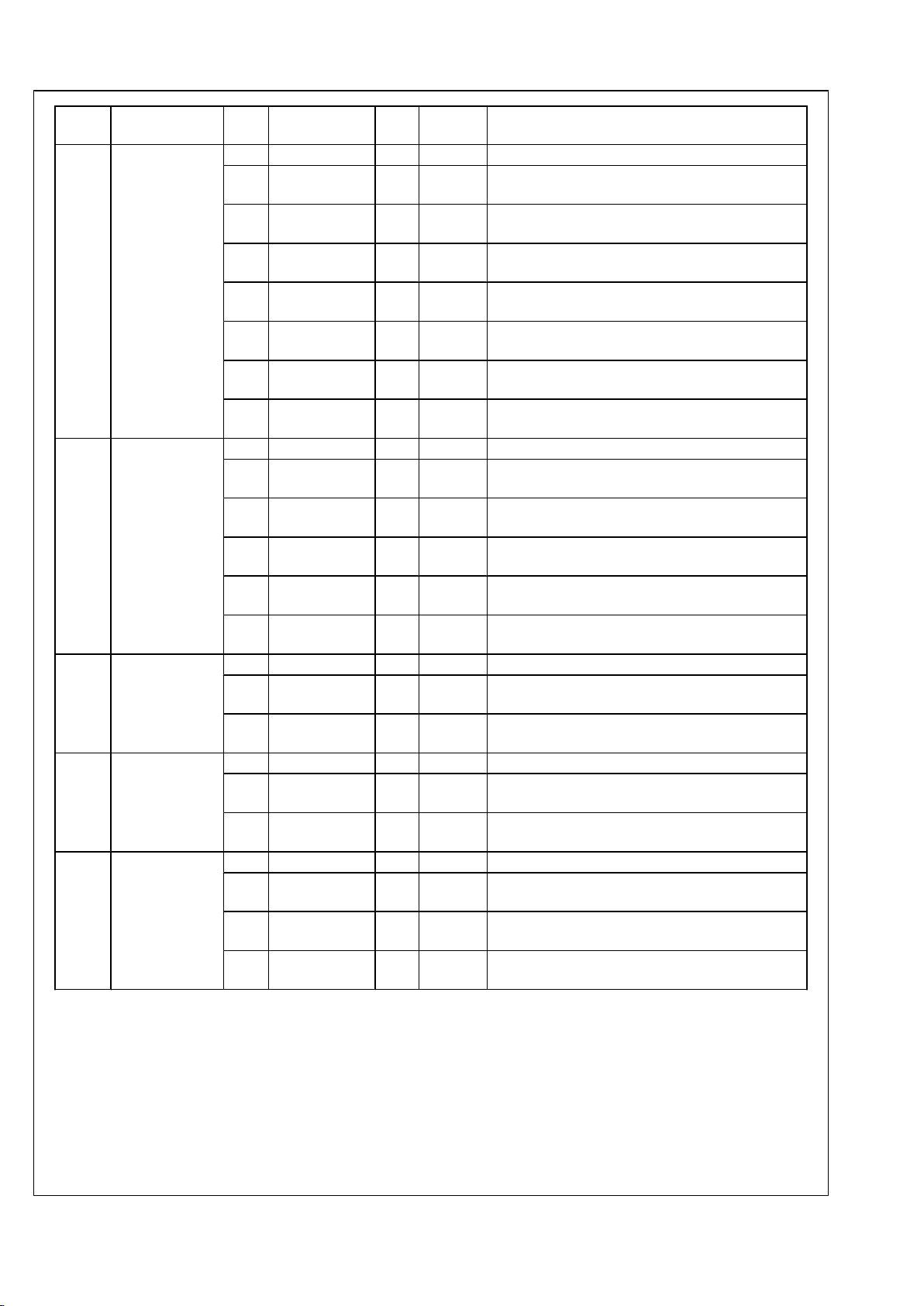
Register Map
The register information for the serializer is shown in the table
below. Some registers have been omitted or marked as re-
served; these are for internal testing and should not be written
to. Some register bits require an override bit to be set before
they can be written to.
Addr
(Hex)
Name Bits Field R/W Default Description
00 Device ID 7:1 SMBus Address R/W 57'h Some systems will use all 8 bits as the device ID. This
will shift the value from 57’h to AE’h
0 Reserved
01 Reset 7:5 Reserved
4 Analog Disable R/W 0 Disables analog blocks. Power save feature
3:1 Reserved
0 Software Reset Reset the device. Does not affect device ID.
02 GPIO0 Config 7:4 GPIO0 Mode R/W 0 0000: GP out register
0001: Link loss indicator
0011: TxCLKIN loss of signal
0100: TxCLKIN detect
All others: Reserved
3:2 GPIO0 R Enable R/W 01'b 00: Pullup/down disabled
01: Pulldown enabled
10: Pullup enabled
11: Reserved
1 Input Enable R/W 0 0: Input buffer disabled
1: Input buffer enabled
0 Output Enable R/W 1'b 0: OutputTtri-State™
1: Output enabled
03 GPIO1 Config 7:4 GPIO1 Mode R/W 0 0000: Power on reset
0001: GP out register
0010: PLL lock indicator
0011: TxIN0 loss of signal
0100: TxIN1 loss of signal
0101: TxIN2 loss of signal
0110: TxIN3 loss of signal
0111: TxIN4 loss of signal
All others: Reserverd
3:2 GPIO1 R Enable R/W 01'b 00: Pullup/down disabled
01: Pulldown enabled
10: Pullup enabled
11: Reserved
1 Input Enable R/W 0 0: Input buffer disabled
1: Input buffer enabled
0 Output Enable R/W 1'b 0: Output Tri-State™
1: Output enabled
04 GPIO2 Config 7:4 GPIO2 Mode R/W 0 0000: GP out register
0001: Always on clock out
0010: Parallel-to-serial clock out
0100: Digital clock out
All others: Reserverd
3:2 GPIO2 R Enable R/W 01'b 00: Pullup/down disabled
01: Pulldown enabled
10: Pullup enabled
11: Reserved
1 Input Enable R/W 0 0: Input buffer disabled
1: Input buffer enabled
0 Output Enable R/W 1'b 0: Output Tri-State™
1: Output enabled
19 www.national.com
DS32EL0421, DS32ELX0421
Page 20

Addr
(Hex)
Name Bits Field R/W Default Description
05 GP In 7:3 Reserved
2 GP In 2 R 0 Input value on GPIO2
1 GP In 1 R 0 Input value on GPIO1
0 GP In 0 R 0 Input value on GPIO0
06 GP Out 7:3 Reserved
2 GP Out 2 R/W 0 Output value on GPIO2
1 GP Out 1 R/W 0 Output value on GPIO1
0 GP Out 0 R/W 0 Output value on GPIO0
07–1F Reserved
20 De-Emphasis 7:3 Reserved
2 Pin Override R/W 0 0: Pin values determine setting
1: Register overrides pin values
1:0 De-emphasis
level
R/W 0 00: No de-emphasis
01: Low
10: Medium
11: High
21 Device Config 7 NRZ enable R/W 0 Enable NRZ, if override bit is set
6 DV disable R/W 0 Disable Data Valid
5 Reserved R/W 0
4 Scrambler
Enable
R/W 0 Scrambler control, requires override bit to change
setting
3 DC Bal encoder
bypass
R/W 0 Bypass encoder, requires override bit to change
setting
2 Training
Sequence
Enable
R/W 0 Enable training sequence, requires override bit to
change setting
1:0 Device
Configuration
R/W 0 MSB: Remote Sense enable, active low
LSB: DC balance encoder enable, active low
Requires override bit to change settings through
registers. Normally controlled by pins
22 Device Config
Override
7:5 Reserved
4 NRZ bypass
override
R/W 0 Unlock reg 21’h bit 7
3 Scrambler
bypass override
R/W 0 Unlock reg 21’h bit 4
2 DC Bal encoder
bypass override
R/W 0 Unlock reg 21’h bit 3
1 Training
sequence
enable override
R/W 0 Unlock reg 21’h bit 2
0 Config pin
override
R/W 0 Unlock reg 21’h bits 1 and 0
23 Reserved
24 LVDS Clock
Delay Enable
7 TxCLKIN Delay
Bypass
R/W 0 0: TxCLKIN delay enable
1: Bypass TxCLKIN delay
6:0 Reserved
25 Reserved
www.national.com 20
DS32EL0421, DS32ELX0421
Page 21
Addr
(Hex)
Name Bits Field R/W Default Description
26 Power Down 7 Channel Reset R/W 0 Reset high speed channel. Self-clearing bit.
6 Clock
Powerdown
R/W 0 Power down parallel, parallel-to-serial, and always on
clock
5 LVDS Clock
enable
R/W 1'b 0: Disable TxCLKIN
1: Enable TxCLKIN
4 TxIN4 Enable R/W 1'b 0: Disable TxIN4
1: Enable TxIN4
3 TxIN3 Enable R/W 1'b 0: Disable TxIN3
1: Enable TxIN3
2 TxIN2 Enable R/W 1'b 0: Disable TxIN2
1: Enable TxIN2
1 TxIN1 Enable R/W 1'b 0: Disable TxIN1
1: Enable TxIN1
0 TxIN0 Enable R/W 1'b 0: Disable TxIN0
1: Enable TxIN0
27 Event Disable 7:5 Reserved R/W 0
4 PLL Lock
Disable
R/W 0 0: Count clock errors
1: Clock error count disabled
3 FIFO Error
Disable
R/W 0 0: Count FIFO erros 1: FIFO error count disabled
2 Parallel Clock
Detect Disable
R/W 0 0: Count clock detect errors
1: Clock detect count disabled
1 Clock Loss of
Signal Disable
R/W 0 0: Count clock los of signal errors
1: Clock loss of signal count disabled
0 Data Loss of
Signal Disable
R/W 0 0: Count data los of signal errors
1: Clock data of signal count disabled
28 LVDS Operation 7:2 Reserved
1 LVDS Loss of
Signal Preset
R/W 0 Preset signal for LVDS loss of signal register
0 LVDS Loss of
Signal Reset
R/W 0 Clear signal for LVDS loss of signal register
29 Loss of Signal
Status
7:6 Reserved
5 Clock Loss of
Signal
R 0 0: No clock present on TxCLKIN
1: Clock present
4:0 Data Loss of
Signal
R 0 0: No data present on TxIN4:0
1: Data present
2A Event Status 7:4 Reserved
3 TxCLKIN Detect R/W 0 0: TxCLKIN not detected
1: TxCLKIN detected
2 PLL Lock R/W 0 0: PLL not locked
1: PLL locked
1:0 Link Detect 1:0 R/W 0 0: Link not detected
1: Link detected
21 www.national.com
DS32EL0421, DS32ELX0421
Page 22

Addr
(Hex)
Name Bits Field R/W Default Description
2B Event Config 7 Reserved
6 PLL Lock Event R/W 0 0: Count PLL lock events
1: Do not count PLL lock events
5 Link Event R/W 0 0: Count link events
1: Do not count link events
4 Loss of Signal
Event
R/W 0 0: Count loss of signal events
1: Do not count loss of signal events
3 Event Count
Select
R/W 0 0: Select PLL event count for reading
1: Select link event count for reading
2 Clear PLL Error
Count
R/W 0 1: Reset PLL error count. Self clearing bit.
1 Clear Link Error
Count
R/W 0 1: Reset link error count. Self clearing bit.
0 Enable Count R/W 0 0: Disable event counters
1: Enable event counters
2C Event Count 7:0 Event Counter R 0
2D Reserved
2E Analog Driver 7 Reserved
6 Reverse Data
Order
R/W 0 0: Normal
1: Reverse output data order
5:2 Reserved R/W 0
1 Link Detect 1 R/W 0 Link detect value for channel 1
0 Link Detect 0 R/W 0 Link detect value for channel 0
2F Tx Config 7:6 Reserved
5 Output
Termination
R/W 1'b
0: 75 Ω terminations
1: 50 Ω terminations
4:3 Reserved
2 TxOUT Override R/W 0 0: TxOUT0 enabled by default, TxOUT1_en pin
controls channel1
1: Override enable of TxOUT0 and TxOUT1
1 TxOUT1 Enable R/W 0 0: TxOUT1 disabled
1: TxOUT1 enabled
0 TxOOUT0
Enable
R/W 0 0: TxOUT0 disabled
1: TxOUT0 enabled
30 Clock Delay 7:5 TxCLKIN Delay R/W 011’b 000: No clock delay
111: Max clock delay, 1000 ps
See t
LVDL
in LVDS Switching Characteristics for more
details
4:0 Reserved 00010’b
31–68 Reserved
69 Output Amplitude
Adjust
7:3 Reserved
2:0 Amplitude Adjust R/W 011’b 000: Level 7
001: Level 8 (Highest output)
010: Level 5
011: Level 6 (Normal output)
100: Level 4
101: Level 3
110: Level 2
111: Level 1 (Lowest output)
www.national.com 22
DS32EL0421, DS32ELX0421
Page 23

Register Recipes
Many features of the serializer contained within the SMBus
registers require multiple writes to configure and enable. This
methodology was implemented to prevent accidental register
writes from causing undesired device behavior. Several
recipes for common features are listed below. When experimenting with other SMBus register features, be sure to read
through the register map for override and enable bits.
SCRAMBLER OVERRIDE CONTROL
The scrambler’s default settings are described in the device
configuration section. However, the scrambler’s setting can
be overridden if desired.
Reg 22’h, write 08’h
Reg 21’h, write to bit 3 to enable/disable
75Ω MODE
The serialzer can be programmed to interface with 75Ω media
by using the recipe shown below. The inverting serial output
should be terminated when interfacing with single ended media.
Reg 2F’h, write 0 to bit 5
OUTPUT CHANNEL MUX CONTROL
DS32ELX0421 only. TxOUT0 is the output channel enabled
by default. By using the external pin TxOUT1_EN, TxOUT1
will be activated along with TxOUT0. If an application requires
that only one channel be active at a time, the following recipe
allows for each channel to be enabled or disabled independent of the other.
Reg 2F’h, write 1’b to bit 2
Reg 2F’h, write to bits 1 or 0 to control the output channels
OUTPUT THE SERIAL CLOCK ON GPIO2
It is very helpful to be able to monitor high speed communication systems and observe their signal integrity. Generally,
this is done with a high speed real time oscilloscope or a
sampling oscilloscope. Sampling oscilloscopes require a reference clock to trigger on. The following recipe can be used
to bring out the serial clock on GPIO2 to provide a trigger for
sampling oscilloscopes.
Reg 04’h, write 21’h
Power Save Mode
When a system does not need to transmit high speed data
from the DS32EL0421 or DS32ELX0421, the power consumption of the device can be managed as described in the
Power Management section on the Functional Description
page. The following recipe powers down many of the analog
and digital blocks in the serializer, but leaves the SMBus
module operational. Please note that in order to resume normal operation the recipe below will have to be unwritten.
Reg 01'h, write 10'h
Reg 26'h, write 40'h
23 www.national.com
DS32EL0421, DS32ELX0421
Page 24

Physical Dimensions inches (millimeters) unless otherwise noted
48–Lead LLP Plastic Quad Package
NS Package Number SQA48A
(See AN-1187 for PCB Design and Assembly Recommendations)
www.national.com 24
DS32EL0421, DS32ELX0421
Page 25

Notes
25 www.national.com
DS32EL0421, DS32ELX0421
Page 26
Notes
DS32EL0421, DS32ELX0421 125 – 312.5 MHz Serializer with DDR LVDS Parallel LVDS Interface
For more National Semiconductor product information and proven design tools, visit the following Web sites at:
Products Design Support
Amplifiers www.national.com/amplifiers WEBENCH www.national.com/webench
Audio www.national.com/audio Analog University www.national.com/AU
Clock Conditioners www.national.com/timing App Notes www.national.com/appnotes
Data Converters www.national.com/adc Distributors www.national.com/contacts
Displays www.national.com/displays Green Compliance www.national.com/quality/green
Ethernet www.national.com/ethernet Packaging www.national.com/packaging
Interface www.national.com/interface Quality and Reliability www.national.com/quality
LVDS www.national.com/lvds Reference Designs www.national.com/refdesigns
Power Management www.national.com/power Feedback www.national.com/feedback
Switching Regulators www.national.com/switchers
LDOs www.national.com/ldo
LED Lighting www.national.com/led
PowerWise www.national.com/powerwise
Serial Digital Interface (SDI) www.national.com/sdi
Temperature Sensors www.national.com/tempsensors
Wireless (PLL/VCO) www.national.com/wireless
THE CONTENTS OF THIS DOCUMENT ARE PROVIDED IN CONNECTION WITH NATIONAL SEMICONDUCTOR CORPORATION
(“NATIONAL”) PRODUCTS. NATIONAL MAKES NO REPRESENTATIONS OR WARRANTIES WITH RESPECT TO THE ACCURACY
OR COMPLETENESS OF THE CONTENTS OF THIS PUBLICATION AND RESERVES THE RIGHT TO MAKE CHANGES TO
SPECIFICATIONS AND PRODUCT DESCRIPTIONS AT ANY TIME WITHOUT NOTICE. NO LICENSE, WHETHER EXPRESS,
IMPLIED, ARISING BY ESTOPPEL OR OTHERWISE, TO ANY INTELLECTUAL PROPERTY RIGHTS IS GRANTED BY THIS
DOCUMENT.
TESTING AND OTHER QUALITY CONTROLS ARE USED TO THE EXTENT NATIONAL DEEMS NECESSARY TO SUPPORT
NATIONAL’S PRODUCT WARRANTY. EXCEPT WHERE MANDATED BY GOVERNMENT REQUIREMENTS, TESTING OF ALL
PARAMETERS OF EACH PRODUCT IS NOT NECESSARILY PERFORMED. NATIONAL ASSUMES NO LIABILITY FOR
APPLICATIONS ASSISTANCE OR BUYER PRODUCT DESIGN. BUYERS ARE RESPONSIBLE FOR THEIR PRODUCTS AND
APPLICATIONS USING NATIONAL COMPONENTS. PRIOR TO USING OR DISTRIBUTING ANY PRODUCTS THAT INCLUDE
NATIONAL COMPONENTS, BUYERS SHOULD PROVIDE ADEQUATE DESIGN, TESTING AND OPERATING SAFEGUARDS.
EXCEPT AS PROVIDED IN NATIONAL’S TERMS AND CONDITIONS OF SALE FOR SUCH PRODUCTS, NATIONAL ASSUMES NO
LIABILITY WHATSOEVER, AND NATIONAL DISCLAIMS ANY EXPRESS OR IMPLIED WARRANTY RELATING TO THE SALE
AND/OR USE OF NATIONAL PRODUCTS INCLUDING LIABILITY OR WARRANTIES RELATING TO FITNESS FOR A PARTICULAR
PURPOSE, MERCHANTABILITY, OR INFRINGEMENT OF ANY PATENT, COPYRIGHT OR OTHER INTELLECTUAL PROPERTY
RIGHT.
LIFE SUPPORT POLICY
NATIONAL’S PRODUCTS ARE NOT AUTHORIZED FOR USE AS CRITICAL COMPONENTS IN LIFE SUPPORT DEVICES OR
SYSTEMS WITHOUT THE EXPRESS PRIOR WRITTEN APPROVAL OF THE CHIEF EXECUTIVE OFFICER AND GENERAL
COUNSEL OF NATIONAL SEMICONDUCTOR CORPORATION. As used herein:
Life support devices or systems are devices which (a) are intended for surgical implant into the body, or (b) support or sustain life and
whose failure to perform when properly used in accordance with instructions for use provided in the labeling can be reasonably expected
to result in a significant injury to the user. A critical component is any component in a life support device or system whose failure to perform
can be reasonably expected to cause the failure of the life support device or system or to affect its safety or effectiveness.
National Semiconductor and the National Semiconductor logo are registered trademarks of National Semiconductor Corporation. All other
brand or product names may be trademarks or registered trademarks of their respective holders.
Copyright© 2008 National Semiconductor Corporation
For the most current product information visit us at www.national.com
National Semiconductor
Americas Technical
Support Center
Email: support@nsc.com
Tel: 1-800-272-9959
National Semiconductor Europe
Technical Support Center
Email: europe.support@nsc.com
German Tel: +49 (0) 180 5010 771
English Tel: +44 (0) 870 850 4288
National Semiconductor Asia
Pacific Technical Support Center
Email: ap.support@nsc.com
National Semiconductor Japan
Technical Support Center
Email: jpn.feedback@nsc.com
www.national.com
 Loading...