

Page 1
AVAILABLE
For pricing, delivery, and
ordering information, please contact Maxim Direct
at 1-888-629-4642, or visit Maxim’s website at www.maximintegrated.com.
General Description
The DS3231 is a low-cost, extremely accurate I2C realtime clock (RTC) with an integrated temperaturecompensated crystal oscillator (TCXO) and crystal. The
device incorporates a battery input, and maintains accurate timekeeping when main power to the device is interrupted. The integration of the crystal resonator enhances
the long-term accuracy of the device as well as reduces
the piece-part count in a manufacturing line. The DS3231
is available in commercial and industrial temperature
ranges, and is offered in a 16-pin, 300-mil SO package.
The RTC maintains seconds, minutes, hours, day, date,
month, and year information. The date at the end of the
month is automatically adjusted for months with fewer
than 31 days, including corrections for leap year. The
clock operates in either the 24-hour or 12-hour format
with an AM/PM indicator. Two programmable time-ofday alarms and a programmable square-wave output
are provided. Address and data are transferred serially
through an I
2
C bidirectional bus.
A precision temperature-compensated voltage reference and comparator circuit monitors the status of V
CC
to detect power failures, to provide a reset output, and
to automatically switch to the backup supply when necessary. Additionally, the RST pin is monitored as a
pushbutton input for generating a µP reset.
Applications
Servers Utility Power Meters
Telematics GPS
Features
♦ Accuracy ±2ppm from 0°C to +40°C
♦ Accuracy ±3.5ppm from -40°C to +85°C
♦ Battery Backup Input for Continuous
Timekeeping
♦ Operating Temperature Ranges
Commercial: 0°C to +70°C
Industrial: -40°C to +85°C
♦ Low-Power Consumption
♦ Real-Time Clock Counts Seconds, Minutes,
Hours, Day, Date, Month, and Year with Leap Year
Compensation Valid Up to 2100
♦ Two Time-of-Day Alarms
♦ Programmable Square-Wave Output
♦ Fast (400kHz) I
2
C Interface
♦ 3.3V Operation
♦ Digital Temp Sensor Output: ±3°C Accuracy
♦ Register for Aging Trim
♦ RST Output/Pushbutton Reset Debounce Input
♦ Underwriters Laboratories (UL) Recognized
Extremely Accurate I2C-Integrated
RTC/TCXO/Crystal
19-5170; Rev 8; 7/10
Ordering Information
Pin Configuration appears at end of data sheet.
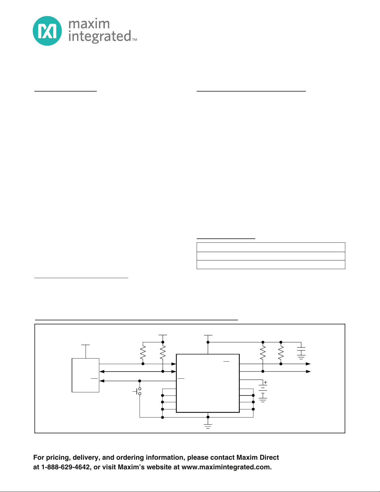
Typical Operating Circuit
#Denotes a RoHS-compliant device that may include lead that
is exempt under RoHS requirements. The lead finish is JESD97
category e3, and is compatible with both lead-based and leadfree soldering processes. A "#" anywhere on the top mark
denotes a RoHS-compliant device.
DS3231
PART TEMP RANGE PIN-PACKAGE
DS3231S# 0°C to +70°C 16 SO
DS3231SN# -40°C to +85°C 16 SO
V
R
= tR/C
V
CC
SCL
SDA
μP
RST
PUSHBUTTON
PU
RESET
CC
B
R
R
PU
PU
SCL
SDA
RST
N.C.
N.C.
N.C.
N.C.
V
CC
V
CC
DS3231
GND
INT/SQW
32kHz
V
BAT
N.C.
N.C.
N.C.
N.C.
Page 2
Extremely Accurate I2C-Integrated
RTC/TCXO/Crystal
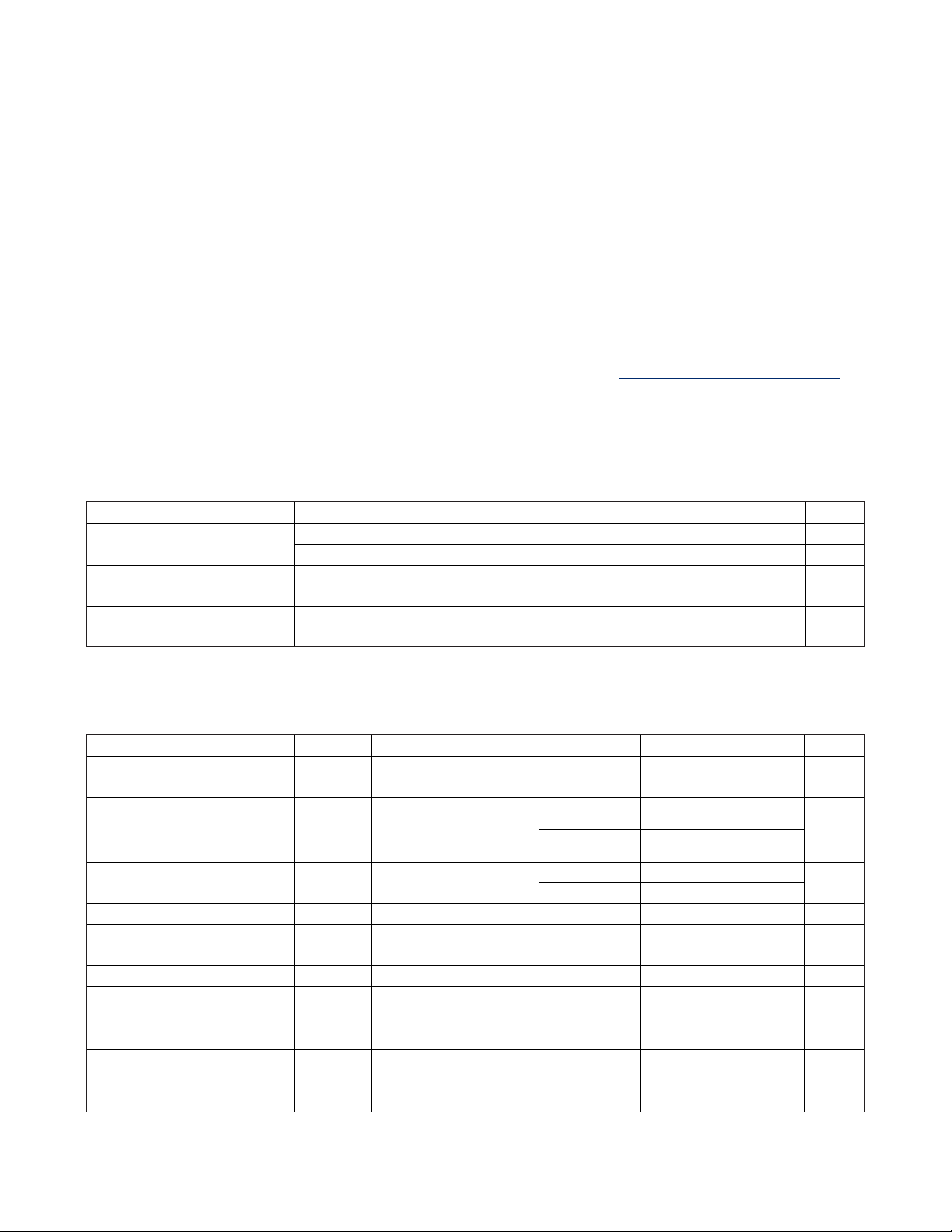
ABSOLUTE MAXIMUM RATINGS
RECOMMENDED OPERATING CONDITIONS
(TA= T
MIN
to T
MAX
, unless otherwise noted.) (Notes 2, 3)
Stresses beyond those listed under “Absolute Maximum Ratings” may cause permanent damage to the device. These are stress ratings only, and functional
operation of the device at these or any other conditions beyond those indicated in the operational sections of the specifications is not implied. Exposure to
absolute maximum rating conditions for extended periods may affect device reliability.
Voltage Range on VCC, V
BAT
, 32kHz, SCL, SDA, RST,
INT/SQW Relative to Ground.............................-0.3V to +6.0V
Junction-to-Ambient Thermal Resistance (θ
JA
) (Note 1)....73°C/W
Junction-to-Case Thermal Resistance (θ
JC
) (Note 1) ......23°C/W
Operating Temperature Range
(noncondensing) .............................................-40°C to +85°C
Junction Temperature......................................................+125°C
Storage Temperature Range ...............................-40°C to +85°C
Lead Temperature (soldering, 10s) .................................+260°C
Soldering Temperature (reflow, 2 times max)
Lead(Pb)-free...............................................................+260°C
Containing lead(Pb) .....................................................+240°C
(See the
Handling, PC Board Layout, and Assembly
section.)
ELECTRICAL CHARACTERISTICS
(VCC= 2.3V to 5.5V, VCC= Active Supply (see Table 1), TA= T
MIN
to T
MAX
, unless otherwise noted.) (Typical values are at V
CC
=
3.3V, V
BAT
= 3.0V, and TA= +25°C, unless otherwise noted.) (Notes 2, 3)
Note 1: Package thermal resistances were obtained using the method described in JEDEC specification JESD51-7, using a four-
layer board. For detailed information on package thermal considerations, refer to www.maxim-ic.com/thermal-tutorial
.
DS3231
2
Maxim Integrated
Supply Voltage
Logic 1 Input SDA, SCL V
Logic 0 Input SDA, SCL VIL -0.3
PARAMETER SYMBOL CONDITIONS MIN TYP MAX UNITS
VCC 2.3 3.3 5.5 V
2.3 3.0 5.5 V
V
BAT
IH
0.7 x
V
CC
VCC +
0.3
0.3 x
V
CC
V
V
Active Supply Current I
Standby Supply Current I
Temperature Conversion Current I
Power-Fail Voltage VPF 2.45 2.575 2.70 V
Logic 0 Output, 32kHz,
INT/SQW, SDA
Logic 0 Output, RST V
Output Leakage Current 32kHz,
INT/SQW, SDA
Input Leakage SCL ILI -1 +1 μA
RST Pin I/O Leakage I
V
BAT
(V
PARAMETER SYMBOL CONDITIONS MIN TYP MAX UNITS
(Notes 4, 5)
CCA
I2C bus inactive, 32kHz
output on, SQW output off
(Note 5)
I2C bus inactive, 32kHz
output on, SQW output off
IOL = 3mA 0.4 V
IOL = 1mA 0.4 V
Output high impedance -1 0 +1 μA
RST high impedance (Note 6) -200 +10 μA
25 100 nA
Leakage Current
Active)
CC
CCS
CCSCONV
V
OL
OL
I
LO
OL
I
BATLKG
VCC = 3.63V 200
= 5.5V 300
V
CC
VCC = 3.63V 110
V
= 5.5V 170
CC
VCC = 3.63V 575
V
= 5.5V 650
CC
μA
μA
μA
Page 3
Extremely Accurate I2C-Integrated
RTC/TCXO/Crystal
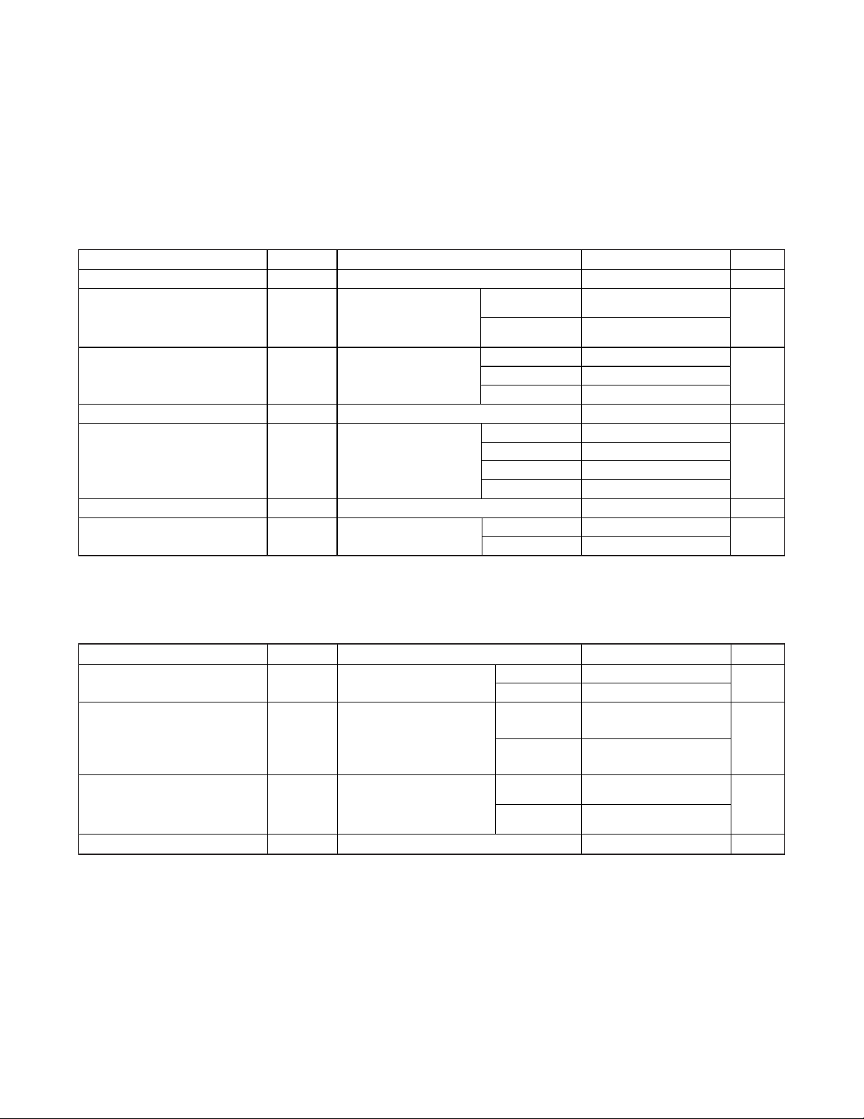
ELECTRICAL CHARACTERISTICS (continued)
(VCC= 2.3V to 5.5V, VCC= Active Supply (see Table 1), TA= T
MIN
to T
MAX
, unless otherwise noted.) (Typical values are at V
CC
=
3.3V, V
BAT
= 3.0V, and TA= +25°C, unless otherwise noted.) (Notes 2, 3)
ELECTRICAL CHARACTERISTICS
(VCC= 0V, V
BAT
= 2.3V to 5.5V, TA= T
MIN
to T
MAX
, unless otherwise noted.) (Note 2)
DS3231
Maxim Integrated
3
Output Frequency f
Frequency Stabilit y vs.
Temperature (Commercial)
Frequency Stabilit y vs.
Temperature (Industrial)
Frequency Stabilit y vs. Voltage f/V 1 ppm/V
Trim Register Frequency
Sensitivity per LSB
Temperature Accuracy Temp VCC = 3.3V or V
Crystal Aging f/f
PARAMETER SYMBOL CONDITIONS MIN TYP MAX UNITS
VCC = 3.3V or V
OUT
VCC = 3.3V or
= 3.3V,
f/f
f/f
f/LSB Specif ied at:
V
OUT
OUT
BAT
aging offset = 00h
VCC = 3.3V or
V
BAT
aging offset = 00h
After reflow,
O
not production te sted
= 3.3V,
BAT
BAT
= 3.3V 32.768 kHz
0°C to +40°C ±2
>40°C to +70°C ±3.5
-40°C to <0°C ±3.5
0°C to +40°C ±2
>40°C to +85°C ±3.5
-40°C 0.7
+25°C 0.1
+70°C 0.4
+85°C 0.8
= 3.3V -3 +3 °C
First year ±1.0
0–10 years ±5.0
ppm
ppm
ppm
ppm
Active Battery Current I
Timekeeping Battery Current I
Temperature Conversion Current I
Data-Retention Current I
PARAMETER SYMBOL CONDITIONS MIN TYP MAX UNITS
BATA
BATT
BATTC
BATTDR
V
= 3.63V 70
EOSC = 0, BBSQW = 0,
SCL = 400kHz (Note 5)
EOSC = 0, BBSQW = 0,
EN32kHz = 1,
SCL = SDA = 0V or
SCL = SDA = V
EOSC = 0, BBSQW = 0,
SCL = SDA = 0V or
SCL = SDA = V
EOSC = 1, SCL = SDA = 0V, +25°C 100 nA
(Note 5)
BAT
V
BAT
BAT
V
= 5.5V 150
BAT
V
= 3.63V 0.84 3.0
BAT
V
= 5.5V 1.0 3.5
BAT
V
= 3.63V 575
BAT
= 5.5V 650
BAT
μA
μA
μA
Page 4

Extremely Accurate I2C-Integrated
RTC/TCXO/Crystal
AC ELECTRICAL CHARACTERISTICS
(VCC= V
CC(MIN)
to V
CC(MAX)
or V
BAT
= V
BAT(MIN)
to V
BAT(MAX)
, V
BAT
> VCC, TA= T
MIN
to T
MAX
, unless otherwise noted.) (Note 2)
POWER-SWITCH CHARACTERISTICS
(TA= T
MIN
to T
MAX
)
DS3231
4
Maxim Integrated
SCL Clock Frequency f
Bus Free Time Between STOP
and START Conditions
Hold Time (Repeated) START
Condition (Note 7)
Low Period of SCL Cloc k t
High Period of SCL Clock t
Data Hold Time (Notes 8, 9) t
Data Setup Time (Note 10) t
START Setup Time t
Rise Time of Both SDA and SCL
Signals (Note 11)
Fal l Time of Both SDA and SCL
Signals (Note 11)
Setup Time for STOP Condition t
Capacitive Load for Each Bus
Line
Capacitance for SDA, SCL C
Pulse Width of Spikes That Must
Be Suppressed by the Input Filter
Pushbutton Debounce PBDB 250 ms
Reset Active Time t
Oscillator Stop Flag (OSF) Delay t
Temperature Conver sion Time t
PARAMETER SYMBOL CONDITIONS MIN TYP MAX UNITS
SCL
t
BUF
t
HD: STA
LOW
HIGH
HD:DAT
SU:DAT
SU:STA
t
t
SU:STO
C
I/O
t
SP
RST
OSF
CONV
Fast mode 100 400
Standard mode 0 100
Fast mode 1.3
Standard mode 4.7
Fast mode 0.6
Standard mode 4.0
Fast mode 1.3
Standard mode 4.7
Fast mode 0.6
Standard mode 4.0
Fast mode 0 0.9
Standard mode 0 0.9
Fast mode 100
Standard mode 250
Fast mode 0.6
Standard mode 4.7
Fast mode 300
R
Standard mode
Fast mode 300
F
Standard mode
20 +
0.1C
20 +
0.1C
B
1000
B
300
Fast mode 0.6
Standard mode 4.7
(Note 11) 400 pF
B
10 pF
30 ns
250 ms
(Note 12) 100 ms
125 200 m s
kHz
μs
μs
μs
μs
μs
ns
μs
ns
ns
μs
VCC Fall Time; V
V
PF(MIN)
VCC Rise Time; V
V
PF(MAX)
Recovery at Power-Up t
PARAMETER SYMBOL CONDITIONS MIN TYP MAX UNITS
to
PF(MAX)
PF(MIN)
to
t
300 μs
VCCF
t
0 μs
VCCR
(Note 13) 250 300 ms
REC
Page 5
Extremely Accurate I2C-Integrated
RTC/TCXO/Crystal
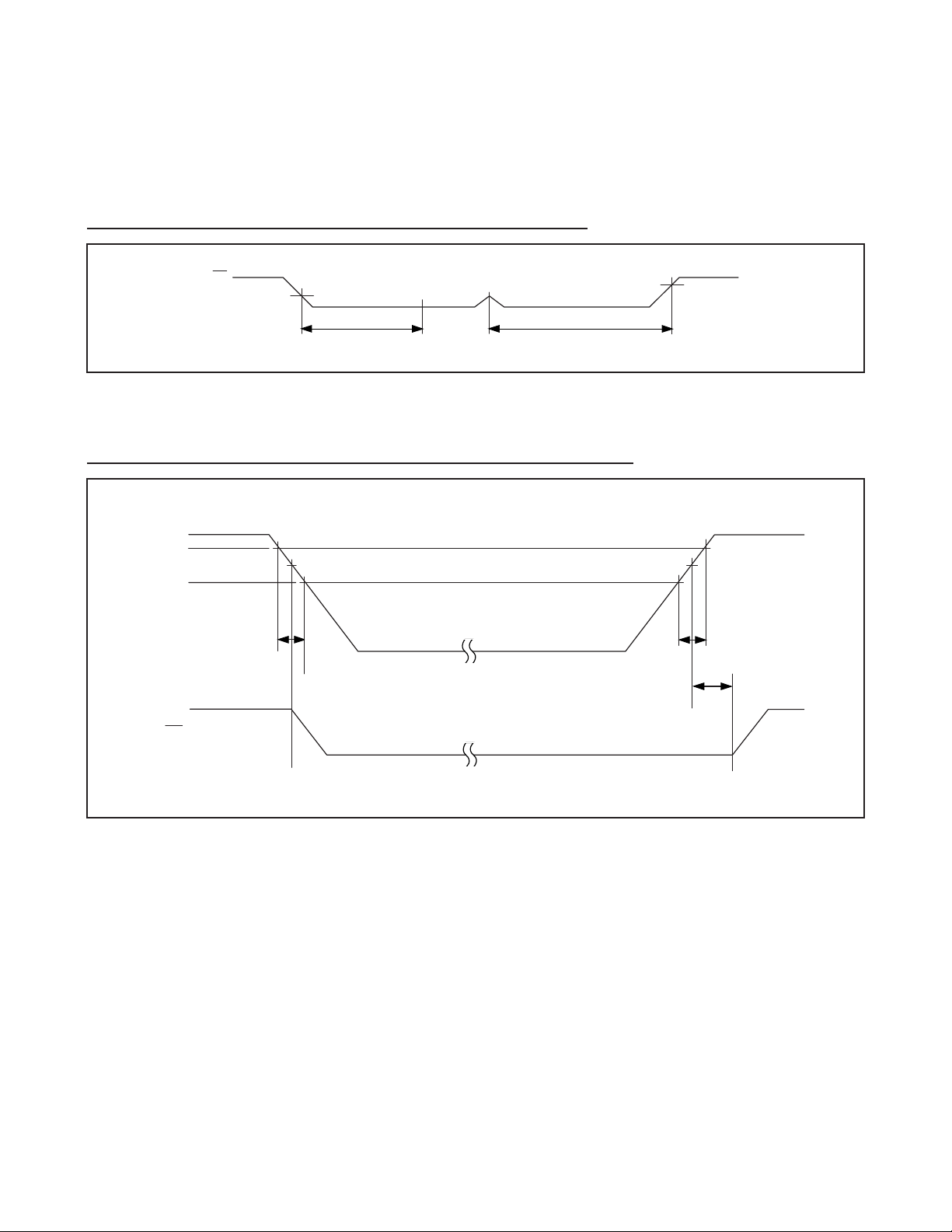
Pushbutton Reset Timing
RST
Power-Switch Timing
DS3231
Maxim Integrated
5
V
PF(MAX)
V
PF(MIN)
V
RST
PB
DB
t
RST
CC
V
PF
t
VCCR
t
REC
t
VCCF
V
PF
Page 6
Extremely Accurate I2C-Integrated
RTC/TCXO/Crystal
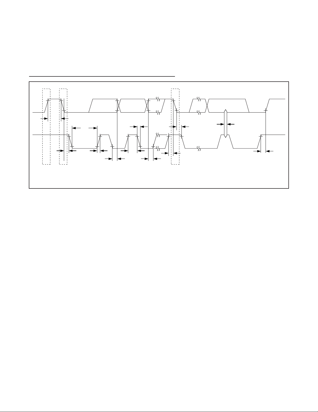
Data Transfer on I2C Serial Bus
WARNING: Negative undershoots below -0.3V while the part is in battery-backed mode may cause loss of data.
Note 2: Limits at -40°C are guaranteed by design and not production tested.
Note 3: All voltages are referenced to ground.
Note 4: I
CCA
—SCL clocking at max frequency = 400kHz.
Note 5: Current is the averaged input current, which includes the temperature conversion current.
Note 6: The RST pin has an internal 50kΩ (nominal) pullup resistor to V
CC
.
Note 7: After this period, the first clock pulse is generated.
Note 8: A device must internally provide a hold time of at least 300ns for the SDA signal (referred to the V
IH(MIN)
of the SCL signal)
to bridge the undefined region of the falling edge of SCL.
Note 9: The maximum t
HD:DAT
needs only to be met if the device does not stretch the low period (t
LOW
) of the SCL signal.
Note 10: A fast-mode device can be used in a standard-mode system, but the requirement t
SU:DAT
≥ 250ns must then be met. This
is automatically the case if the device does not stretch the low period of the SCL signal. If such a device does stretch the
low period of the SCL signal, it must output the next data bit to the SDA line t
R(MAX)
+
t
SU:DAT
= 1000 + 250 = 1250ns
before the SCL line is released.
Note 11: C
B
—total capacitance of one bus line in pF.
Note 12: The parameter t
OSF
is the period of time the oscillator must be stopped for the OSF flag to be set over the voltage range of
0.0V ≤ V
CC
≤ V
CC(MAX)
and 2.3V ≤ V
BAT
≤ 3.4V.
Note 13: This delay applies only if the oscillator is enabled and running. If the EOSC bit is a 1, t
REC
is bypassed and RST immedi-
ately goes high. The state of RST does not affect the I2C interface, RTC, or TCXO.
DS3231
6
Maxim Integrated
SDA
t
BUF
t
LOW
SCL
t
HD:STA
STOP START REPEATED
NOTE: TIMING IS REFERENCED TO V
IL(MAX)
AND V
IH(MIN)
t
R
t
HD:DAT
.
t
HIGH
t
F
t
SU:DAT
START
t
SU:STA
t
HD:STA
t
SP
t
SU:STO
Page 7
Extremely Accurate I2C-Integrated
RTC/TCXO/Crystal
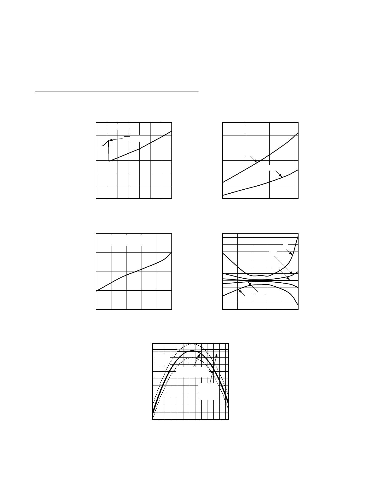
Typical Operating Characteristics
(VCC= +3.3V, TA = +25°C, unless otherwise noted.)
STANDBY SUPPLY CURRENT
vs. SUPPLY VOLTAGE
DS3231 toc01
VCC (V)
I
CCS
(μA)
5.04.54.03.53.02.5
25
50
75
100
125
150
0
2.0 5.5
RST ACTIVE
BSY = 0, SCL = SDA = V
CC
SUPPLY CURRENT
vs. SUPPLY VOLTAGE
DS3231 toc02
V
BAT
(V)
I
BAT
(μA)
5.34.33.3
0.7
0.8
0.9
1.0
1.1
1.2
0.6
2.3
VCC = 0V, BSY = 0,
SDA = SCL = V
BAT
OR V
CC
EN32kHz = 1
EN32kHz = 0
SUPPLY CURRENT
vs. TEMPERATURE
DS3231 toc03
TEMPERATURE (°C)
I
BAT
(μA)
603510-15
0.7
0.8
0.9
1.0
0.6
-40 85
VCC = 0, EN32kHz = 1, BSY = 0,
SDA = SCL = V
BAT
OR GND
FREQUENCY DEVIATION
vs. TEMPERATURE vs. AGING VALUE
DS3231 toc04
TEMPERATURE (°C)
FREQUENCY DEVIATION (ppm)
603510-15
-30
-20
-10
0
10
20
30
40
50
60
-40
-40 85
127
32
0
-33
8
DELTA TIME AND FREQUENCY
vs. TEMPERATURE
TEMPERATURE (°C)
DELTA FREQUENCY (ppm)
DELTA TIME (MIN/YEAR)
807050 60-10 0 10 20 30 40-30 -20
-180
-160
-140
-120
-100
-80
-60
-40
-20
0
20
-200
-80
-60
-40
-20
0
-100
-40
DS3231 toc05
CRYSTAL
+20ppm
CRYSTAL
-20ppm
TYPICAL CRYSTAL,
UNCOMPENSATED
DS3231
ACCURACY
BAND
DS3231
Maxim Integrated
7
Page 8
Extremely Accurate I2C-Integrated
RTC/TCXO/Crystal
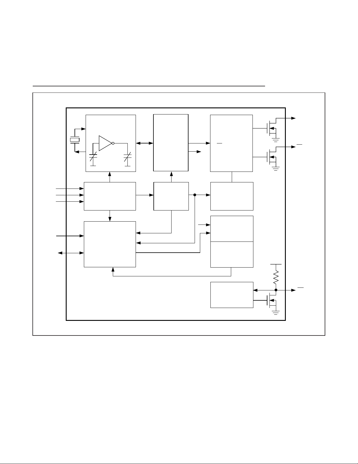
Block Diagram
DS3231
8
Maxim Integrated
V
V
GND
SCL
SDA
BAT
OSCILLATOR AND
X1
CAPACITOR ARRAY
CONTROL LOGIC/
X2
CC
POWER CONTROL
2
C INTERFACE AND
I
ADDRESS REGISTER
DECODE
DIVIDER
1Hz
TEMPERATURE
SENSOR
SQUARE-WAVE BUFFER;
INT/SQW CONTROL
ALARM, STATUS, AND
CONTROL REGISTERS
1Hz
CLOCK AND CALENDAR
REGISTERS
USER BUFFER
(7 BYTES)
N
N
V
CC
32kHz
INT/SQW
DS3231
VOLTAGE REFERENCE;
DEBOUNCE CIRCUIT;
PUSHBUTTON RESET
RST
N
Page 9

Extremely Accurate I2C-Integrated
RTC/TCXO/Crystal
Pin Description
PIN NAME FUNCTION
1 32kHz
32kHz Output. Thi s open-drain pin requires an external pullup res istor. When enabled, the output operates
on either power supply. It may be left open if not used.
2 V
CC
DC Power Pin for Primary Power Supply. This pin should be decoupled using a 0.1μF to 1.0μF capacitor.
If not used, connect to ground.
3 INT/SQW
Active-Low Interrupt or Square-Wave Output. This open-drain pin requires an external pullup resi stor
connected to a supply at 5.5V or less. This multifunction pin is determined by the state of the INTCN bit in
the Control Regi ster (0Eh). When INTCN is set to logic 0, this pin outputs a square wave and its frequency
is determined by RS2 and RS1 bits. When INTCN is set to logic 1, then a match between the timekeeping
registers and either of the alarm registers activates the INT/SQW pin (if the alarm is enabled). Because the
INTCN bit is set to logic 1 when power is first applied, the pin defaults to an interrupt output with alarms
disabled. The pul lup voltage can be up to 5.5V, regardless of the voltage on V
CC
. If not used, th is pin can
be left unconnected.
4 RST
Active-Low Re set. This pin is an open-drain input/output. It indicates the status of V
CC
relative to the
V
PF
specification. As VCC falls below VPF, the RST pin is driven low. When VCC exceeds VPF, for t
RST
, the RST
pin is pulled high by the internal pullup resistor. The active-low, open-drain output is combined with a
debounced pushbutton input function. This pin can be activated by a pushbutton reset request. It ha s an
internal 50k nominal value pul lup resistor to V
CC
. No external pullup resistors should be connected. If the
oscillator is disabled, t
REC
is b ypassed and RST immediately goes high.
5–12 N.C. No Connection. Must be connected to ground.
13 GND Ground
14 V
BAT
Backup Power-Supply Input. When using the device with the V
BAT
input a s the primary power source, this
pin should be decoupled using a 0.1μF to 1.0μF low-leakage capacitor. When using the device with the
V
BAT
input as the backup power source, the capacitor is not required. If V
BAT
is not used, connect to ground.
The device is UL recognized to ensure against reverse charging when used with a primary lithium battery.
Go to www.maxim-ic.com/qa/info/ul
.
15 SDA
Serial Data Input/Output. Thi s pin i s the data input/output for the I
2
C serial in terface. This open-drain pin
requires an external pullup resistor. The pullup voltage can be up to 5.5V, regardless of the voltage on V
CC
.
16 SCL
Serial Clock Input. This pin is the cloc k input for the I
2
C serial interface and is used to synchronize data
movement on the serial interface. Up to 5.5V can be used for this pin, regardle ss of the voltage on V
CC
.
Detailed Description
The DS3231 is a serial RTC driven by a temperaturecompensated 32kHz crystal oscillator. The TCXO provides a stable and accurate reference clock, and
maintains the RTC to within ±2 minutes per year accuracy from -40°C to +85°C. The TCXO frequency output
is available at the 32kHz pin. The RTC is a low-power
clock/calendar with two programmable time-of-day
alarms and a programmable square-wave output. The
INT/SQW provides either an interrupt signal due to
alarm conditions or a square-wave output. The clock/calendar provides seconds, minutes, hours, day, date,
month, and year information. The date at the end of the
month is automatically adjusted for months with fewer
than 31 days, including corrections for leap year. The
clock operates in either the 24-hour or 12-hour format
with an AM/PM indicator. The internal registers are
accessible though an I
2
C bus interface.
A temperature-compensated voltage reference and
comparator circuit monitors the level of VCCto detect
power failures and to automatically switch to the backup supply when necessary. The RST pin provides an
external pushbutton function and acts as an indicator
of a power-fail event.
Operation
The block diagram shows the main elements of the
DS3231. The eight blocks can be grouped into four
functional groups: TCXO, power control, pushbutton
function, and RTC. Their operations are described separately in the following sections.
DS3231
Maxim Integrated
9
Page 10

Extremely Accurate I2C-Integrated
RTC/TCXO/Crystal
32kHz TCXO
The temperature sensor, oscillator, and control logic
form the TCXO. The controller reads the output of the
on-chip temperature sensor and uses a lookup table to
determine the capacitance required, adds the aging
correction in AGE register, and then sets the capacitance selection registers. New values, including
changes to the AGE register, are loaded only when a
change in the temperature value occurs, or when a
user-initiated temperature conversion is completed.
Temperature conversion occurs on initial application of
VCCand once every 64 seconds afterwards.
Power Control
This function is provided by a temperature-compensated voltage reference and a comparator circuit that
monitors the VCClevel. When VCCis greater than VPF,
the part is powered by V
CC
. When VCCis less than V
PF
but greater than V
BAT
, the DS3231 is powered by VCC.
If VCCis less than VPFand is less than V
BAT
, the
device is powered by V
BAT
. See Table 1.
To preserve the battery, the first time V
BAT
is applied to
the device, the oscillator will not start up until V
CC
exceeds VPF, or until a valid I2C address is written to
the part. Typical oscillator startup time is less than one
second. Approximately 2 seconds after VCCis applied,
or a valid I2C address is written, the device makes a
temperature measurement and applies the calculated
correction to the oscillator. Once the oscillator is running, it continues to run as long as a valid power
source is available (VCCor V
BAT
), and the device continues to measure the temperature and correct the
oscillator frequency every 64 seconds.
On the first application of power (VCC) or when a valid
I2C address is written to the part (V
BAT
), the time and
date registers are reset to 01/01/00 01 00:00:00
(MM/DD/YY DOW HH:MM:SS).
V
BAT
Operation
There are several modes of operation that affect the
amount of V
BAT
current that is drawn. While the device
is powered by V
BAT
and the serial interface is active,
active battery current, I
BATA
, is drawn. When the serial
interface is inactive, timekeeping current (I
BATT
), which
includes the averaged temperature conversion current,
I
BATTC
, is used (refer to Application Note 3644:
Power
Considerations for Accurate Real-Time Clocks
for
details). Temperature conversion current, I
BATTC
, is
specified since the system must be able to support the
periodic higher current pulse and still maintain a valid
voltage level. Data retention current, I
BATTDR
, is the
current drawn by the part when the oscillator is
stopped (EOSC = 1). This mode can be used to minimize battery requirements for times when maintaining
time and date information is not necessary, e.g., while
the end system is waiting to be shipped to a customer.
Pushbutton Reset Function
The DS3231 provides for a pushbutton switch to be
connected to the RST output pin. When the DS3231 is
not in a reset cycle, it continuously monitors the RST
signal for a low going edge. If an edge transition is
detected, the DS3231 debounces the switch by pulling
the RST low. After the internal timer has expired
(PBDB), the DS3231 continues to monitor the RST line.
If the line is still low, the DS3231 continuously monitors
the line looking for a rising edge. Upon detecting
release, the DS3231 forces the RST pin low and holds it
low for t
RST
.
RST is also used to indicate a power-fail condition.
When VCCis lower than VPF, an internal power-fail signal is generated, which forces the RST pin low. When
VCCreturns to a level above VPF, the RST pin is held
low for approximately 250ms (t
REC
) to allow the power
supply to stabilize. If the oscillator is not running (see
the
Power Control
section) when VCCis applied, t
REC
is
bypassed and RST immediately goes high. Assertion of
the RST output, whether by pushbutton or power-fail
detection, does not affect the internal operation of the
DS3231.
Real-Time Clock
With the clock source from the TCXO, the RTC provides
seconds, minutes, hours, day, date, month, and year
information. The date at the end of the month is automatically adjusted for months with fewer than 31 days,
including corrections for leap year. The clock operates
in either the 24-hour or 12-hour format with an AM/PM
indicator.
The clock provides two programmable time-of-day
alarms and a programmable square-wave output. The
INT/SQW pin either generates an interrupt due to alarm
condition or outputs a square-wave signal and the
selection is controlled by the bit INTCN.
Table 1. Power Control
DS3231
10
Maxim Integrated
SUPPLY CONDITION ACTIVE SUPPLY
VCC < VPF, VCC < V
VCC < VPF, VCC > V
VCC > VPF, VCC < V
VCC > VPF, VCC > V
V
BAT
V
BAT
V
BAT
V
BAT
BAT
CC
CC
CC
Page 11
Extremely Accurate I2C-Integrated
RTC/TCXO/Crystal
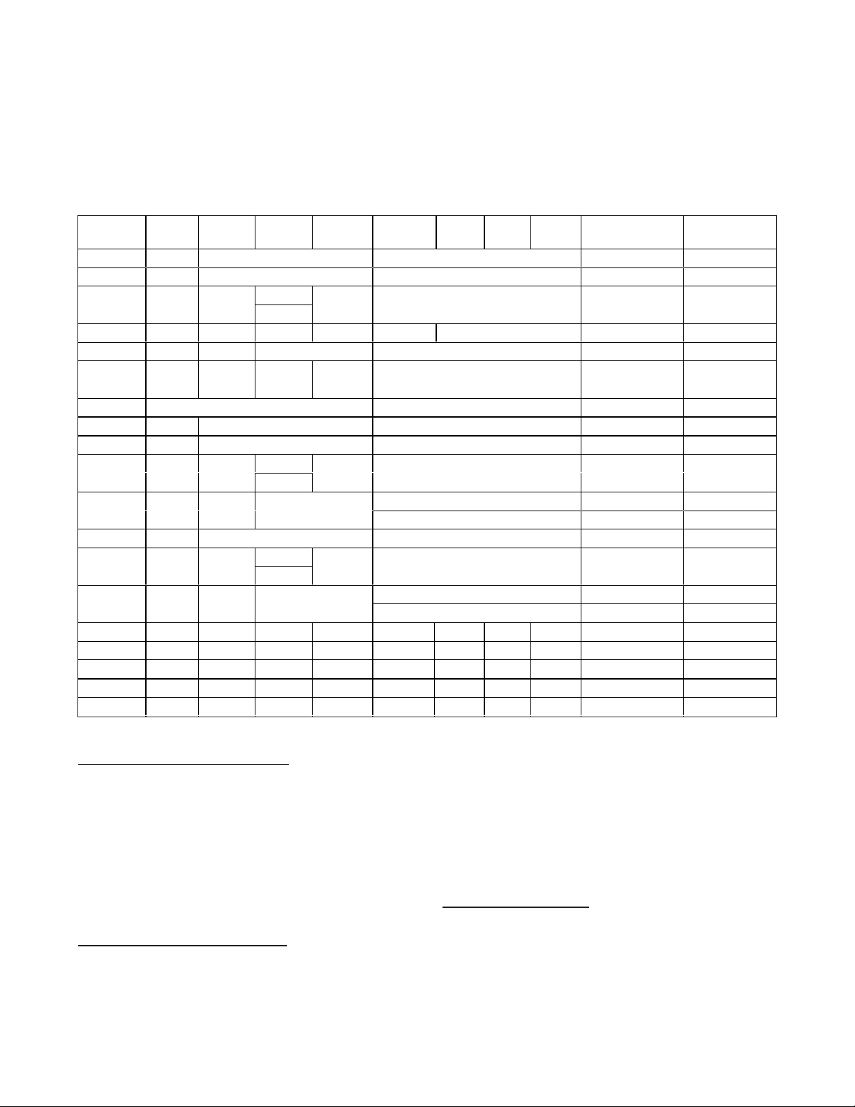
Figure 1. Timekeeping Registers
Note: Unless otherwise specified, the registers’ state is not defined when power is first applied.
Address Map
Figure 1 shows the address map for the DS3231 timekeeping registers. During a multibyte access, when the
address pointer reaches the end of the register space
(12h), it wraps around to location 00h. On an I2C
START or address pointer incrementing to location 00h,
the current time is transferred to a second set of registers. The time information is read from these secondary
registers, while the clock may continue to run. This
eliminates the need to reread the registers in case the
main registers update during a read.
I
2
C Interface
The I2C interface is accessible whenever either VCCor
V
BAT
is at a valid level. If a microcontroller connected
to the DS3231 resets because of a loss of VCCor other
event, it is possible that the microcontroller and
DS3231 I
2
C communications could become unsynchronized, e.g., the microcontroller resets while reading data from the DS3231. When the microcontroller
resets, the DS3231 I2C interface may be placed into a
known state by toggling SCL until SDA is observed to
be at a high level. At that point the microcontroller
should pull SDA low while SCL is high, generating a
START condition.
Clock and Calendar
The time and calendar information is obtained by reading the appropriate register bytes. Figure 1 illustrates
the RTC registers. The time and calendar data are set
or initialized by writing the appropriate register bytes.
The contents of the time and calendar registers are in
DS3231
Maxim Integrated
11
A D D R ESS
00h 0 10 Seconds Seconds Seconds 00–59
01h 0 10 Minutes Minutes Minutes 00–59
02h 0 12/24
03h 0 0 0 0 0 Day Day 1–7
04h 0 0 10 Date Date Date 01–31
05h Century 0 0 10 Month Month
06h 10 Year Year Year 00–99
07h A1M1 10 Seconds Seconds Alarm 1 Seconds 00–59
08h A1M2 10 Minutes Minutes Alarm 1 Minutes 00–59
09h A1M3 12/24
0Ah A1M4 DY/DT 10 Date
0Bh A2M2 10 Minutes Minutes Alarm 2 Minutes 00–59
0Ch A2M3 12/24
0Dh A2M4 DY/DT 10 Date
0Eh EOSC BBSQW CONV RS2 RS1 INTCN A2IE A1IE Control —
0Fh OSF 0 0 0 EN32kHz BSY A2F A1F Control/Status —
10h SIGN DATA DATA DATA DATA DATA DATA DATA Aging Offset —
11h SIGN DATA DATA DATA DATA DATA DATA DATA MSB of Temp —
12h DATA DATA 0 0 0 0 0 0 LSB of Temp —
BIT 7
MSB
BIT 6 BIT 5 BIT 4 BIT 3 BIT 2 BIT 1
AM/PM
20 Hour
AM/PM
20 Hour
AM/PM
20 Hour
10 Hour Hour Hours
10 Hour Hour Alarm 1 Hours
Day Alarm 1 Day 1–7
Date Alarm 1 Date 1–31
10 Hour Hour Alarm 2 Hours
Day Alarm 2 Day 1–7
Date Alarm 2 Date 1–31
BIT 0
LSB
FUNCTION RANGE
Month/
Century
1–12 + AM/PM
00–23
01–12 +
Century
1–12 + AM/PM
00–23
1–12 + AM/PM
00–23
Page 12

the binary-coded decimal (BCD) format. The DS3231
can be run in either 12-hour or 24-hour mode. Bit 6 of
the hours register is defined as the 12- or 24-hour
mode select bit. When high, the 12-hour mode is
selected. In the 12-hour mode, bit 5 is the AM/PM bit
with logic-high being PM. In the 24-hour mode, bit 5 is
the 20-hour bit (20–23 hours). The century bit (bit 7 of
the month register) is toggled when the years register
overflows from 99 to 00.
The day-of-week register increments at midnight.
Values that correspond to the day of week are userdefined but must be sequential (i.e., if 1 equals
Sunday, then 2 equals Monday, and so on). Illogical
time and date entries result in undefined operation.
When reading or writing the time and date registers, secondary (user) buffers are used to prevent errors when
the internal registers update. When reading the time and
date registers, the user buffers are synchronized to the
internal registers on any START and when the register
pointer rolls over to zero. The time information is read
from these secondary registers, while the clock continues to run. This eliminates the need to reread the registers in case the main registers update during a read.
The countdown chain is reset whenever the seconds register is written. Write transfers occur on the acknowledge
from the DS3231. Once the countdown chain is reset, to
avoid rollover issues the remaining time and date registers
must be written within 1 second. The 1Hz square-wave output, if enabled, transitions high 500ms after the seconds
data transfer, provided the oscillator is already running.
Alarms
The DS3231 contains two time-of-day/date alarms.
Alarm 1 can be set by writing to registers 07h to 0Ah.
Alarm 2 can be set by writing to registers 0Bh to 0Dh.
The alarms can be programmed (by the alarm enable
and INTCN bits of the control register) to activate the
INT/SQW output on an alarm match condition. Bit 7 of
each of the time-of-day/date alarm registers are mask
bits (Table 2). When all the mask bits for each alarm
are logic 0, an alarm only occurs when the values in the
timekeeping registers match the corresponding values
stored in the time-of-day/date alarm registers. The
alarms can also be programmed to repeat every second, minute, hour, day, or date. Table 2 shows the possible settings. Configurations not listed in the table will
result in illogical operation.
The DY/DT bits (bit 6 of the alarm day/date registers)
control whether the alarm value stored in bits 0 to 5 of
that register reflects the day of the week or the date of
the month. If DY/DT is written to logic 0, the alarm will
be the result of a match with date of the month. If
DY/DT is written to logic 1, the alarm will be the result of
a match with day of the week.
When the RTC register values match alarm register settings, the corresponding Alarm Flag ‘A1F’ or ‘A2F’ bit is
set to logic 1. If the corresponding Alarm Interrupt
Enable ‘A1IE’ or ‘A2IE’ is also set to logic 1 and the
INTCN bit is set to logic 1, the alarm condition will activate the INT/SQW signal. The match is tested on the
once-per-second update of the time and date registers.
Extremely Accurate I2C-Integrated
RTC/TCXO/Crystal
Table 2. Alarm Mask Bits
DS3231
12
Maxim Integrated
DY/DT
DY/DT
ALARM 1 REGISTER MASK BITS (BIT 7)
A1M4 A1M3 A1M2 A1M1
X 1 1 1 1 Alarm once per second
X 1 1 1 0 Alarm when seconds match
X 1 1 0 0 Alarm when minute s and seconds match
X 1 0 0 0 Alarm when hour s, minute s, and seconds match
0 0 0 0 0 Alarm when date, hours, minutes, and seconds match
1 0 0 0 0 Alarm when day, hours, minutes, and seconds match
ALARM 2 REGISTER MASK BITS (BIT 7)
A2M4 A2M3 A2M2
X 1 1 1 Alarm once per minute (00 seconds of every minute)
X 1 1 0 Alarm when minutes match
X 1 0 0 Alarm when hours and minute s match
0 0 0 0 Alarm when date, hours, and minutes match
1 0 0 0 Alarm when day, hours, and minute s match
ALARM RATE
ALARM RATE
Page 13
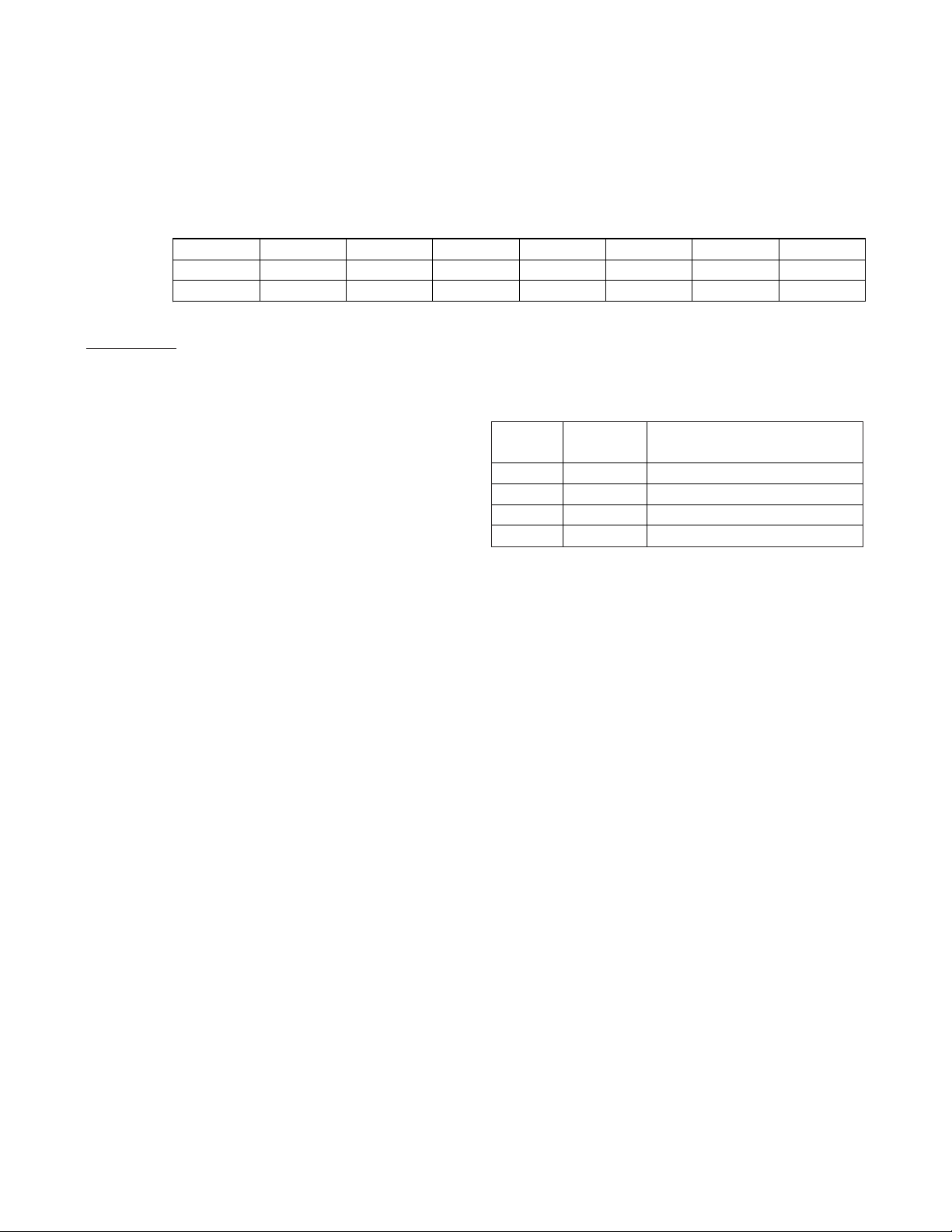
Special-Purpose Registers
The DS3231 has two additional registers (control and
status) that control the real-time clock, alarms, and
square-wave output.
Control Register (0Eh)
Bit 7: Enable Oscillator (EOSC). When set to logic 0,
the oscillator is started. When set to logic 1, the oscillator is stopped when the DS3231 switches to V
BAT
. This
bit is clear (logic 0) when power is first applied. When
the DS3231 is powered by VCC, the oscillator is always
on regardless of the status of the EOSC bit. When
EOSC is disabled, all register data is static.
Bit 6: Battery-Backed Square-Wave Enable
(BBSQW). When set to logic 1 with INTCN = 0 and V
CC
< VPF, this bit enables the square wave. When BBSQW
is logic 0, the INT/SQW pin goes high impedance when
VCC< VPF. This bit is disabled (logic 0) when power is
first applied.
Bit 5: Convert Temperature (CONV). Setting this bit to
1 forces the temperature sensor to convert the temperature into digital code and execute the TCXO algorithm
to update the capacitance array to the oscillator. This
can only happen when a conversion is not already in
progress. The user should check the status bit BSY
before forcing the controller to start a new TCXO execution. A user-initiated temperature conversion does
not affect the internal 64-second update cycle.
A user-initiated temperature conversion does not affect
the BSY bit for approximately 2ms. The CONV bit
remains at a 1 from the time it is written until the conversion is finished, at which time both CONV and BSY go
to 0. The CONV bit should be used when monitoring
the status of a user-initiated conversion.
Bits 4 and 3: Rate Select (RS2 and RS1). These bits
control the frequency of the square-wave output when
the square wave has been enabled. The following table
shows the square-wave frequencies that can be selected with the RS bits. These bits are both set to logic 1
(8.192kHz) when power is first applied.
Bit 2: Interrupt Control (INTCN). This bit controls the
INT/SQW signal. When the INTCN bit is set to logic 0, a
square wave is output on the INT/SQW pin. When the
INTCN bit is set to logic 1, then a match between the
timekeeping registers and either of the alarm registers
activates the INT/SQW output (if the alarm is also
enabled). The corresponding alarm flag is always set
regardless of the state of the INTCN bit. The INTCN bit
is set to logic 1 when power is first applied.
Bit 1: Alarm 2 Interrupt Enable (A2IE). When set to
logic 1, this bit permits the alarm 2 flag (A2F) bit in the
status register to assert INT/SQW (when INTCN = 1).
When the A2IE bit is set to logic 0 or INTCN is set to
logic 0, the A2F bit does not initiate an interrupt signal.
The A2IE bit is disabled (logic 0) when power is first
applied.
Bit 0: Alarm 1 Interrupt Enable (A1IE). When set to
logic 1, this bit permits the alarm 1 flag (A1F) bit in the
status register to assert INT/SQW (when INTCN = 1).
When the A1IE bit is set to logic 0 or INTCN is set to
logic 0, the A1F bit does not initiate the INT/SQW signal. The A1IE bit is disabled (logic 0) when power is
first applied.
Extremely Accurate I2C-Integrated
RTC/TCXO/Crystal
SQUARE-WAVE OUTPUT FREQUENCY
Control Register (0Eh)
DS3231
Maxim Integrated
13
BIT 7 BIT 6 BIT 5 BIT 4 BIT 3 BIT 2 BIT 1 BIT 0
NAME: EOSC BBSQW CONV RS2 RS1 INTCN A2IE A1IE
POR: 0 0 0 1 1 1 0 0
RS2 RS1
0 0 1Hz
0 1 1.024kH z
1 0 4.096kH z
1 1 8.192kH z
SQUARE-WAVE OUTPUT
FREQUENCY
Page 14

Status Register (0Fh)
Bit 7: Oscillator Stop Flag (OSF). A logic 1 in this bit
indicates that the oscillator either is stopped or was
stopped for some period and may be used to judge the
validity of the timekeeping data. This bit is set to logic 1
any time that the oscillator stops. The following are examples of conditions that can cause the OSF bit to be set:
1) The first time power is applied.
2) The voltages present on both VCCand V
BAT
are
insufficient to support oscillation.
3) The EOSC bit is turned off in battery-backed mode.
4) External influences on the crystal (i.e., noise, leak-
age, etc.).
This bit remains at logic 1 until written to logic 0.
Bit 3: Enable 32kHz Output (EN32kHz). This bit controls the status of the 32kHz pin. When set to logic 1, the
32kHz pin is enabled and outputs a 32.768kHz squarewave signal. When set to logic 0, the 32kHz pin goes to
a high-impedance state. The initial power-up state of
this bit is logic 1, and a 32.768kHz square-wave signal
appears at the 32kHz pin after a power source is
applied to the DS3231 (if the oscillator is running).
Bit 2: Busy (BSY). This bit indicates the device is busy
executing TCXO functions. It goes to logic 1 when the
conversion signal to the temperature sensor is asserted
and then is cleared when the device is in the 1-minute
idle state.
Bit 1: Alarm 2 Flag (A2F). A logic 1 in the alarm 2 flag
bit indicates that the time matched the alarm 2 registers. If the A2IE bit is logic 1 and the INTCN bit is set to
logic 1, the INT/SQW pin is also asserted. A2F is
cleared when written to logic 0. This bit can only be
written to logic 0. Attempting to write to logic 1 leaves
the value unchanged.
Bit 0: Alarm 1 Flag (A1F). A logic 1 in the alarm 1 flag
bit indicates that the time matched the alarm 1 regis-
ters. If the A1IE bit is logic 1 and the INTCN bit is set to
logic 1, the INT/SQW pin is also asserted. A1F is
cleared when written to logic 0. This bit can only be
written to logic 0. Attempting to write to logic 1 leaves
the value unchanged.
Aging Offset
The aging offset register takes a user-provided value to
add to or subtract from the codes in the capacitance
array registers. The code is encoded in two’s complement, with bit 7 representing the sign bit. One LSB represents one small capacitor to be switched in or out of
the capacitance array at the crystal pins. The aging offset register capacitance value is added or subtracted
from the capacitance value that the device calculates
for each temperature compensation. The offset register
is added to the capacitance array during a normal temperature conversion, if the temperature changes from
the previous conversion, or during a manual user conversion (setting the CONV bit). To see the effects of the
aging register on the 32kHz output frequency immediately, a manual conversion should be started after each
aging register change.
Positive aging values add capacitance to the array,
slowing the oscillator frequency. Negative values
remove capacitance from the array, increasing the
oscillator frequency.
The change in ppm per LSB is different at different
temperatures. The frequency vs. temperature curve is
shifted by the values used in this register. At +25°C,
one LSB typically provides about 0.1ppm change in
frequency.
Use of the aging register is not needed to achieve the
accuracy as defined in the EC tables, but could be
used to help compensate for aging at a given temperature. See the
Typical Operating Characteristics
section
for a graph showing the effect of the register on accuracy over temperature.
Extremely Accurate I2C-Integrated
RTC/TCXO/Crystal
Aging Offset (10h)
Status Register (0Fh)
DS3231
14
Maxim Integrated
BIT 7 BIT 6 BIT 5 BIT 4 BIT 3 BIT 2 BIT 1 BIT 0
NAME: OSF 0 0 0 EN32kHz BSY A2F A1F
POR: 1 0 0 0 1 X X X
NAME: Sign Data Data Data Data Data Data Data
POR: 0 0 0 0 0 0 0 0
BIT 7 BIT 6 BIT 5 BIT 4 BIT 3 BIT 2 BIT 1 BIT 0
Page 15

Temperature Registers (11h–12h)
Temperature is represented as a 10-bit code with a resolution of 0.25°C and is accessible at location 11h and
12h. The temperature is encoded in two’s complement
format. The upper 8 bits, the integer portion, are at
location 11h and the lower 2 bits, the fractional portion,
are in the upper nibble at location 12h. For example,
00011001 01b = +25.25°C. Upon power reset, the registers are set to a default temperature of 0°C and the
controller starts a temperature conversion. The temperature is read on initial application of VCCor I2C access
on V
BAT
and once every 64 seconds afterwards. The
temperature registers are updated after each user-initiated conversion and on every 64-second conversion.
The temperature registers are read-only.
I2C Serial Data Bus
The DS3231 supports a bidirectional I2C bus and data
transmission protocol. A device that sends data onto
the bus is defined as a transmitter and a device receiving data is defined as a receiver. The device that controls the message is called a master. The devices that
are controlled by the master are slaves. The bus must
be controlled by a master device that generates the
serial clock (SCL), controls the bus access, and generates the START and STOP conditions. The DS3231
operates as a slave on the I2C bus. Connections to the
bus are made through the SCL input and open-drain
SDA I/O lines. Within the bus specifications, a standard
mode (100kHz maximum clock rate) and a fast mode
(400kHz maximum clock rate) are defined. The DS3231
works in both modes.
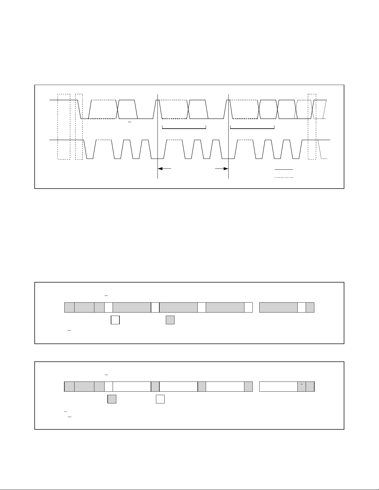
The following bus protocol has been defined (Figure 2):
• Data transfer may be initiated only when the bus is
not busy.
• During data transfer, the data line must remain stable
whenever the clock line is high. Changes in the data
line while the clock line is high are interpreted as
control signals.
Accordingly, the following bus conditions have been
defined:
Bus not busy: Both data and clock lines remain
high.
START data transfer: A change in the state of the
data line from high to low, while the clock line is high,
defines a START condition.
STOP data transfer: A change in the state of the
data line from low to high, while the clock line is high,
defines a STOP condition.
Data valid: The state of the data line represents
valid data when, after a START condition, the data
line is stable for the duration of the high period of the
clock signal. The data on the line must be changed
during the low period of the clock signal. There is
one clock pulse per bit of data.
Each data transfer is initiated with a START condition
and terminated with a STOP condition. The number
of data bytes transferred between the START and
the STOP conditions is not limited, and is determined
by the master device. The information is transferred
byte-wise and each receiver acknowledges with a
ninth bit.
Acknowledge: Each receiving device, when
addressed, is obliged to generate an acknowledge
after the reception of each byte. The master device
must generate an extra clock pulse, which is associated with this acknowledge bit.
A device that acknowledges must pull down the SDA
line during the acknowledge clock pulse in such a
way that the SDA line is stable low during the high
period of the acknowledge-related clock pulse. Of
course, setup and hold times must be taken into
account. A master must signal an end of data to the
Extremely Accurate I2C-Integrated
RTC/TCXO/Crystal
Temperature Register (Upper Byte) (11h)
Temperature Register (Lower Byte) (12h)
DS3231
Maxim Integrated
15
BIT 7 BIT 6 BIT 5 BIT 4 BIT 3 BIT 2 BIT 1 BIT 0
NAME: Sign Data Data Data Data Data Data Data
POR: 0 0 0 0 0 0 0 0
BIT 7 BIT 6 BIT 5 BIT 4 BIT 3 BIT 2 BIT 1 BIT 0
NAME: Data Data 0 0 0 0 0 0
POR: 0 0 0 0 0 0 0 0
Page 16
slave by not generating an acknowledge bit on the
last byte that has been clocked out of the slave. In
this case, the slave must leave the data line high to
enable the master to generate the STOP condition.
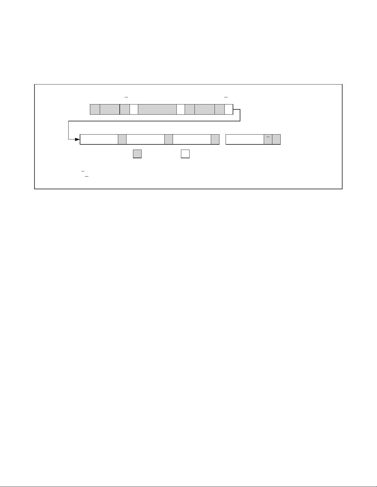
Figures 3 and 4 detail how data transfer is accomplished on the I2C bus. Depending upon the state of
the R/W bit, two types of data transfer are possible:
Data transfer from a master transmitter to a slave
receiver. The first byte transmitted by the master is
the slave address. Next follows a number of data
bytes. The slave returns an acknowledge bit after
each received byte. Data is transferred with the most
significant bit (MSB) first.
Data transfer from a slave transmitter to a master
receiver. The first byte (the slave address) is trans-
mitted by the master. The slave then returns an
acknowledge bit. Next follows a number of data
bytes transmitted by the slave to the master. The
Extremely Accurate I2C-Integrated
RTC/TCXO/Crystal
Figure 2. I2C Data Transfer Overview
Figure 3. Data Write—Slave Receiver Mode
Figure 4. Data Read—Slave Transmitter Mode
DS3231
16
Maxim Integrated
MSB FIRST MSB LSB MSB LSB
SDA
SCL
IDLE
START
CONDITION
SLAVE
ADDRESS
1–7 8 9 1–7 8 9 1–7 8 9
R/W ACK ACKDATA ACK/
REPEATED IF MORE BYTES
<SLAVE
ADDRESS>
S - START
A - ACKNOWLEDGE (ACK)
P - STOP
R/W - READ/WRITE OR DIRECTION BIT ADDRESS
<R/W> <WORD ADDRESS (n)> <DATA (n)> <DATA (n + 1)> <DATA (n + X)
AXXXXXXXXA1101000S 0 XXXXXXXX A XXXXXXXX A XXXXXXXX A P
ARE TRANSFERRED
MASTER TO SLAVESLAVE TO MASTER
DATA
...
DATA TRANSFERRED
(X + 1 BYTES + ACKNOWLEDGE)
NACK
STOP CONDITION
REPEATED START
<SLAVE
ADDRESS>
S - START
A - ACKNOWLEDGE (ACK)
P - STOP
A - NOT ACKNOWLEDGE (NACK)
R/W - READ/WRITE OR DIRECTION BIT ADDRESS
<R/W> <DATA (n)> <DATA (n + 1)> <DATA (n + 2)> <DATA (n + X)>
MASTER TO SLAVE SLAVE TO MASTER
AXXXXXXXXA1101000S 1 XXXXXXXX A XXXXXXXX A XXXXXXXX A P
DATA TRANSFERRED
(X + 1 BYTES + ACKNOWLEDGE)
NOTE: LAST DATA BYTE IS FOLLOWED BY A NACK.
...
Page 17
master returns an acknowledge bit after all received
bytes other than the last byte. At the end of the last
received byte, a not acknowledge is returned.
The master device generates all the serial clock pulses and the START and STOP conditions. A transfer is
ended with a STOP condition or with a repeated
START condition. Since a repeated START condition
is also the beginning of the next serial transfer, the
bus will not be released. Data is transferred with the
most significant bit (MSB) first.
The DS3231 can operate in the following two modes:
Slave receiver mode (DS3231 write mode): Serial
data and clock are received through SDA and SCL.
After each byte is received, an acknowledge bit is
transmitted. START and STOP conditions are recognized as the beginning and end of a serial transfer.
Address recognition is performed by hardware after
reception of the slave address and direction bit. The
slave address byte is the first byte received after the
master generates the START condition. The slave
address byte contains the 7-bit DS3231 address,
which is 1101000, followed by the direction bit (R/W),
which is 0 for a write. After receiving and decoding
the slave address byte, the DS3231 outputs an
acknowledge on SDA. After the DS3231 acknowledges the slave address + write bit, the master
transmits a word address to the DS3231. This sets
the register pointer on the DS3231, with the DS3231
acknowledging the transfer. The master may then
transmit zero or more bytes of data, with the DS3231
acknowledging each byte received. The register
pointer increments after each data byte is transferred. The master generates a STOP condition to
terminate the data write.
Slave transmitter mode (DS3231 read mode): The
first byte is received and handled as in the slave
receiver mode. However, in this mode, the direction
bit indicates that the transfer direction is reversed.
Serial data is transmitted on SDA by the DS3231
while the serial clock is input on SCL. START and
STOP conditions are recognized as the beginning
and end of a serial transfer. Address recognition is
performed by hardware after reception of the slave
address and direction bit. The slave address byte is
the first byte received after the master generates a
START condition. The slave address byte contains
the 7-bit DS3231 address, which is 1101000, followed by the direction bit (R/W), which is 1 for a
read. After receiving and decoding the slave
address byte, the DS3231 outputs an acknowledge
on SDA. The DS3231 then begins to transmit data
starting with the register address pointed to by the
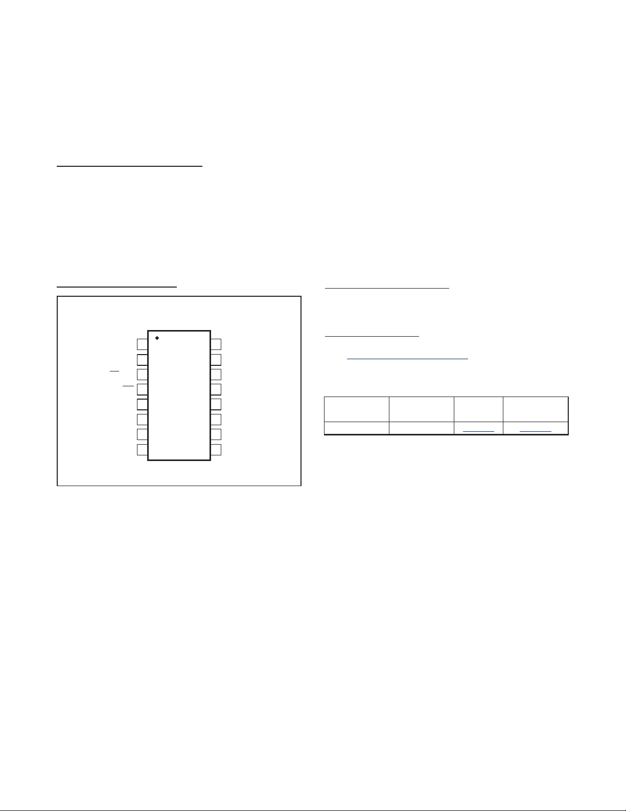
register pointer. If the register pointer is not written to
before the initiation of a read mode, the first address
that is read is the last one stored in the register pointer. The DS3231 must receive a not acknowledge to
end a read.
Extremely Accurate I2C-Integrated
RTC/TCXO/Crystal
Figure 5. Data Write/Read (Write Pointer, Then Read)—Slave Receive and Transmit
DS3231
Maxim Integrated
17
<SLAVE
ADDRESS> <R/W>
<DATA (n)> <DATA (n + 1)> <DATA (n + 2)> <DATA (n + X)>
<R/W> <WORD ADDRESS (n)> <SLAVE ADDRESS (n)>
AXXXXXXXXA1101000 1101000SSr0 A1
AXXXXXXXX XXXXXXXX A XXXXXXXX A XXXXXXXX A P
...
S - START
Sr - REPEATED START
A - ACKNOWLEDGE (ACK)
P - STOP
A - NOT ACKNOWLEDGE (NACK)
R/W - READ/WRITE OR DIRECTION BIT ADDRESS
MASTER TO SLAVE SLAVE TO MASTER
DATA TRANSFERRED
(X + 1 BYTES + ACKNOWLEDGE)
NOTE: LAST DATA BYTE IS FOLLOWED BY A NACK.
Page 18
Extremely Accurate I2C-Integrated
RTC/TCXO/Crystal
Chip Information
SUBSTRATE CONNECTED TO GROUND
PROCESS: CMOS
Package Information
For the latest package outline information and land patterns,
go to www.maxim-ic.com/packages
. Note that a “+”, “#”, or “” in the package code indicates RoHS status only. Package
drawings may show a different suffix character, but the drawing pertains to the package regardless of RoHS status.
Pin Configuration
Handling, PC Board Layout,
and Assembly
The DS3231 package contains a quartz tuning-fork
crystal. Pick-and-place equipment can be used, but
precautions should be taken to ensure that excessive
shocks are avoided. Ultrasonic cleaning should be
avoided to prevent damage to the crystal.
Avoid running signal traces under the package, unless
a ground plane is placed between the package and the
signal line. All N.C. (no connect) pins must be connected to ground.
Moisture-sensitive packages are shipped from the factory dry packed. Handling instructions listed on the
package label must be followed to prevent damage
during reflow. Refer to the IPC/JEDEC J-STD-020 standard for moisture-sensitive device (MSD) classifications
and reflow profiles. Exposure to reflow is limited to 2
times maximum.
PACKAGE
TYPE
PACKAGE
CODE
OUTLINE
NO.
LAND
PATTERN NO.
16 SO W16#H2
21-0042 90-0107
DS3231
18
Maxim Integrated
TOP VIEW
32kHz
V
INT/SQW
RST
N.C.
N.C.
N.C.
N.C.
1
2
CC
3
4
DS3231
5
6
7
8
16
SCL
15
SDA
14
V
BAT
GND
13
N.C.
12
N.C.
11
N.C.
10
N.C.
9
SO
Page 19

Extremely Accurate I2C-Integrated
RTC/TCXO/Crystal
Revision History
DS3231
Maxim Integrated
19
REVISION
NUMBER
0 1/05 Initial release. —
1 2/05
2 6/05
3 11/05 Changed lead-free packages to RoHS-compliant pac kages. 1
4 10/06
5 4/08
REVISION
DATE
DESCRIPTION
Changed Digital Temp Sensor Output from ±2°C to ±3°C. 1, 3
Updated Typical Operating Circuit. 1
Changed TA = -40°C to +85°C to TA = T
Updated Block Diagram. 8
Added “UL Recognized” to Features; added lead-free packages and removed S from
top mark info in Ordering Information table; added ground connections to the N.C. pin
in the Typical Operating Circuit.
Added “noncondensing” to operating temperature range; changed VPF MIN from 2.35V
to 2.45V.
Added aging offset specification. 3
Relabeled TOC4. 7
Added arrow showing input on X1 in the Block Diagram. 8
Updated pin descriptions for VCC and V
Added the I2C Interface section. 10
Figure 1: Added sign bit to aging and temperature registers; added MSB and LSB. 11
Corrected title for rate select bits frequenc y tab le. 13
Added note that frequenc y stabilit y o ver temperature spec is with aging offset regi ster
= 00h; changed bit 7 from Data to Sign (Crystal Aging Offset Register).
Changed bit 7 from Data to Sign (Temperature Register); correct pin definitions in I2C
Serial Data Bus section.
Modified the Handing, PC Board Layout, and Assembly section to refer to
J-STD-020 for reflow profiles for lead-free and leaded packages.
Changed RST and UL bullets in Features. 1
Changed EC condition “VCC > V
Modified Note 12 to correct t
Added various conditions text to TOCs 1, 2, and 3. 7
Added text to pin descriptions for 32kHz, VCC, and RST. 9
Table 1: Changed column heading “Powered By” to “Active Supply”; changed
“applied” to “exceeds V
Indicated BBSQW applie s to both SQW and interrupts; simplified temp convert
description (bit 5); added “output” to INT/SQW (bit 2).
Changed the Crystal Aging section to the Aging Offset section; changed “this bit
indicates” to “this bit controls” for the enable 32kHz output bit.
Added Warning note to EC table notes; updated Note 12. 6
Updated the Typica l Operating Characteri stics graphs. 7
In the Power Control section, added information about the POR state of the ti me and
date registers; in the Real-Time Clock section, added to the description of the RST
function.
In Figure 1, corrected the months date range for 04h from 00 –31 to 01–31. 11
” in the Power Control section.
PF
” to “VCC = Active Supply (see Table 1).” 2, 3
BAT
operation. 6
REC
to T
MIN
. 9
BAT
. 2, 3, 4
MAX
PAGES
CHANGED
1
2
14
15
17
10
13
14
10
Page 20

Extremely Accurate I2C-Integrated
RTC/TCXO/Crystal
Revision History (continued)
DS3231
20
Maxim Integrated 160 Rio Robles, San Jose, CA 95134 USA 1-408-601-1000
Maxim cannot assume responsibility for use of any circuitry other than circuitry entirely embodied in a Maxim product. No circuit patent licenses are implied.
Maxim reserves the right to change the circuitry and specifications without notice at any time. The parametric values (min and max limits) shown in the Electrical
Characteristics table are guaranteed. Other parametric values quoted in this data sheet are provided for guidance.
©
2010 Maxim Integrated
The Maxim logo and Maxim Integrated are trademarks of Maxim Integrated Products, Inc.
REVISION
NUMBER
6 10/08
7 3/10
8 7/10
REVISION
DATE
DESCRIPTION
Updated the Typical Operating Circuit. 1
Removed the VPU parameter from the Recommended DC Operating Conditio ns table
and added verbiage about the pullup to the Pin Description table for INT/SQW, SDA,
and SCL.
Added the Delta Time and Frequenc y vs. Temperature graph in the Typical Operating
Characteri stics section.
Updated the Block Diagram. 8
Added the V
TCXO and Pushbutton Reset Function sections.
Added the register bit POR values to the register tables. 13, 14, 15
Updated the Aging Offset and Temperature Reg isters (11h–12h) sections. 14, 15
Updated the I
Removed the “S” from the top mark in the Ordering Information table and the Pin
Configuration to match the packaging engineering marking specification.
Updated the Typical Operating Circuit; removed the “Top Mark” co lumn from the
Ordering Information; in the Absolute Maximum Ratings sect ion, added the theta-JA
and theta-JC thermal resistances and Note 1, and changed the soldering temperature
to +260°C (lead(Pb)-free) and +240°C (leaded); updated the functional description of
the V
BAT
0Ch to “20 Hour” in Bit 5 of Figure 1; updated the BBSQW bit description in the Control
Register (0Eh) section; added the land pattern no. to the Package Information table.
Operation sect ion, improved some sections of text for the 32kHz
BAT
2
C tim ing diagrams (Figures 3, 4, and 5). 16, 17
pin in the Pin Description; changed the timekeeping registers 02h, 09h, and
PAGES
CHANGED
2, 9
7
10
1, 18
1, 2, 3, 4, 6,
9, 11, 12, 13,
18
 Loading...