

Page 1
A
A
A
Abridged Data Sheet
www.maxim-ic.com
GENERAL DESCRIPTION
The DS28CN01 combines 1024 bits of EEPROM
with challenge-and-response authentication security
implemented with the Federal Information
Publications (FIPS) 180-1/180-2 and ISO/IEC 101183 Secure Hash Algorithm (SHA-1). The memory is
organized as four pages of 32 bytes each. Data
copy-protection and EPROM emulation features are
supported for each memory page. Each DS28CN01
has a guaranteed unique factory-programmed 64-bit
registration number. Communication with the
DS28CN01 is accomplished through an industry
standard I²C- and SMBus™-compatible interface.
The SMBus timeout feature resets the device’s
interface if a bus-timeout fault condition is detected.
APPLICATIONS
Printed Circuit Board (PCB) Unique Serialization
Accessory and Peripheral Identification
Equipment Registration and License Management
Network Node Identification
Printer Cartridge Configuration and Monitoring
Medical Sensor Authentication and Calibration
System Intellectual Property Protection
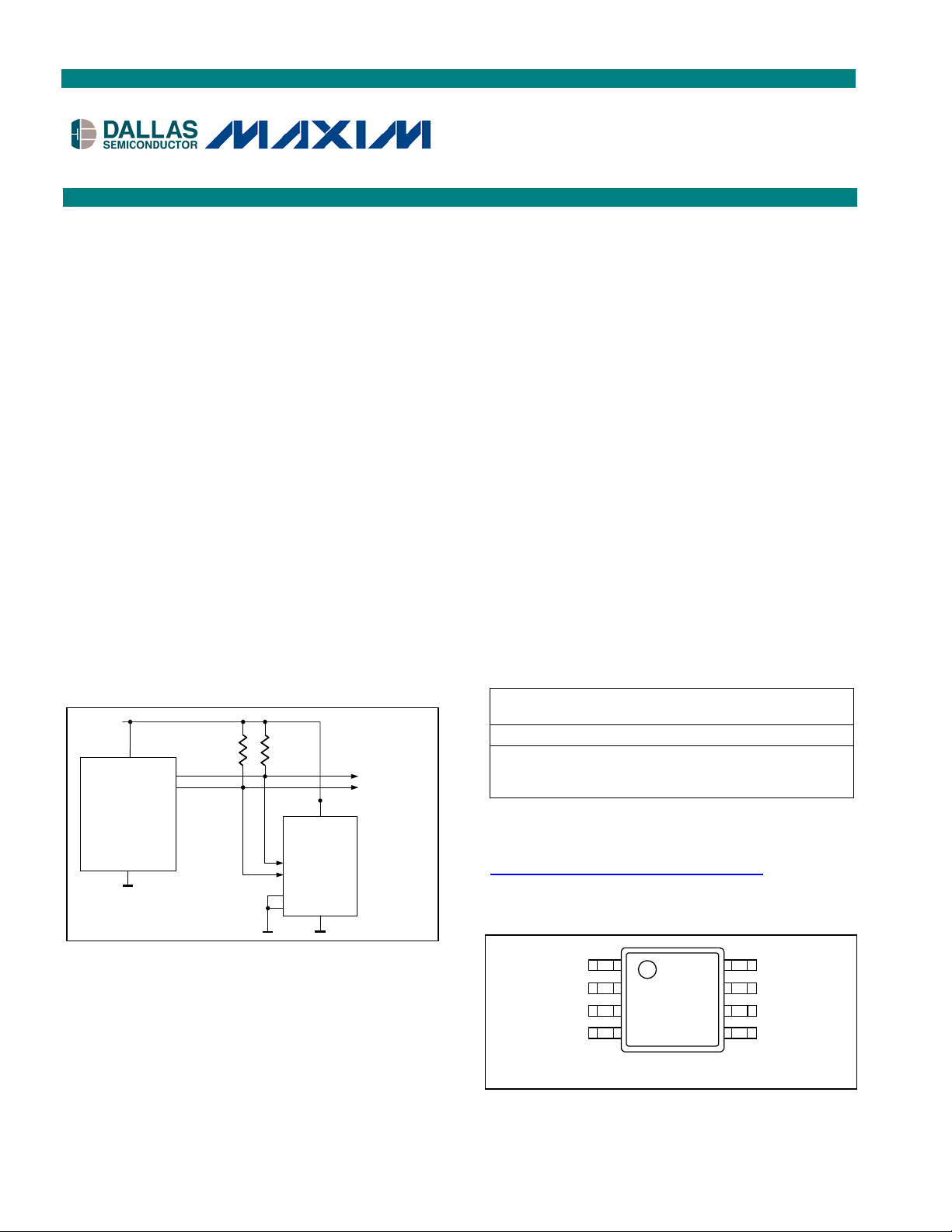
TYPICAL OPERATING CIRCUIT
V
CC
RP R
VCC
SD
SCL
µC
GND
Registers, Modes, and Commands are capitalized for
clarity.
SMBus is a trademark of Intel Corp.
P
VCC
DS28CN01
SDA
SCL
D1
D0 GND
To additional
devices
DS28CN01
1Kbit I²C/SMBus EEPROM
with SHA-1 Engine
FEATURES
1024 Bits of EEPROM Memory Partitioned
Into Four Pages of 256 Bits
Dedicated Hardware-Accelerated SHA Engine
for Generating SHA-1 MACs
EEPROM Memory Pages can be Individually
Copy-Protected or Put Into an EPROM Mode
(Program from 1 to 0 Only)
Write Access Requires Knowledge of the
Secret and the Capability of Computing and
Transmitting a 160-Bit MAC as Authorization
Unique, Factory-Programmed, and Tested
64-Bit Registration Number Assures Absolute
Traceability Because No Two Parts are Alike
Endurance 200k Cycles at +25°C
Serial Interface User Programmable for I²C
Bus and SMBus Compatibility
Supports 100kHz and 400kHz I²C
Communication Speeds
5.5V Tolerant Interface Pins
Operating Range: 1.62V to 5.5V,
-40°C to +85°C
8-Pin µSOP Package
ORDERING INFORMATION
PART TEMP RANGE
DS28CN01U-A00+
DS28CN01U-A00+T
+ Denotes a lead-free package.
-40°C to +85°C
-40°C to +85°C
Request full data sheet at:
www.maxim-ic.com/fullds/DS28CN01
PIN CONFIGURATION
AD0
1
AD1
2
NC
3
GND
4
µSOP
PIN-
PACKAGE
8 µSOP
8 µSOP
Tape-andReel
V
8
CC
7
NC
6
SCL
5
SDA
1 of 9
REV: 061907
Page 2
Abridged Data Sheet DS28CN01
ABSOLUTE MAXIMUM RATINGS
Voltage Range on Any Pin Relative to Ground -0.5V, +6V
Maximum Current Any Pin
Operating Temperature Range
Junction Temperature
±20mA
-40°C to +85°C
+150°C
Storage Temperature Range -55°C to +125°C
Soldering Temperature
Stresses beyond those listed under “Absolute Maximum Ratings” may cause permanent damage to the device. These are stress ratings only,
and functional operation of the device at these or any other conditions beyond those indicated in the operational sections of the specifications is
not implied. Exposure to the absolute maximum rating conditions for extended periods may affect device.
See IPC/JEDEC J-STD-020
ELECTRICAL CHARACTERISTICS (see Note 1)
(TA = -40°C to +85°C)
PARAMETER SYMBOL CONDITIONS MIN TYP MAX UNITS
Supply Voltage V
Standby Current I
Operating Current I
Power-Up Wait Time t
CC
CCS
CCA
POIP
EEPROM
Programming Time t
Programming Current I
Endurance (Notes 3, 4, 5) N
Data Retention (Notes 6, 7, 8) t
PROG
PROG
CY
DR
SHA-1 Engine
SHA Computation Time t
SHA Computation Current I
CSHA
LCSHA
SCL, SDA, AD1, AD0 Pins (Note 9) (See Figure 3)
LOW Level Input Voltage V
HIGH Level Input Voltage V
Hysteresis of Schmitt Trigger
Inputs (Note 2)
LOW Level Output Voltage at
4mA Sink Current, Open Drain
Output Fall Time from V
with a Bus Capacitance
V
ILmax
IHmin
to
from 10pF to 400pF
IL
IH
V
HYS
V
OL
t
OF
(Notes 2, 10)
Pulse Width of Spikes that are
Suppressed by the Input Filter
t
SP
Input Current with an Input
Voltage Between 0.1V
0.9V
CCmax
CC
and
I
i
1.62 5.50 V
Bus idle, VCC = 5.5V 5.5 µA
Bus active at 400kHz,
= 5.5V
V
CC
500 µA
(Note 2) 5 µs
V
≥ 2.0V 10
CC
VCC < 2.0V 45
ms
VCC = 5.5V 1.2 mA
At +25°C 200k
At +85°C 50k
—
At +85°C 40 years
See full version of data
sheet
See full version of data
sheet
VCC ≥ 2.0V
VCC < 2.0V
VCC ≥ 2.0V
VCC < 2.0V
VCC ≥ 2.0V
VCC < 2.0V
VCC ≥ 2.0V
VCC < 2.0V
VCC ≥ 2.0V
VCC < 2.0V
ms
mA
-0.3
-0.3
0.7 ×
V
CC
0.8 ×
V
CC
0.05 ×
V
CC
0.1 ×
V
CC
20 +
0.1C
B
20 +
0.1C
B
0.3 × V
0.25 ×
V
CC
V
CCmax
+0.3V
V
CCmax
+0.3V
CC
0.4
0.2 × V
CC
250
300
V
V
V
V
ns
(Note 2) 50 ns
(Note 11) -10 +10 µA
2 of 9
Page 3
Abridged Data Sheet DS28CN01
PARAMETER SYMBOL CONDITIONS MIN TYP MAX UNITS
Input Capacitance C
SCL Clock Frequency f
Bus Timeout t
SCL
TIMEOUT
I
(Note 2) 10 pF
(Note 12)
400 kHz
(Note 12) 25 75 ms
Hold-Time (Repeated) START
Condition. After this Period, the
t
HD:STA
(Note 13) 0.6 µs
First Clock Pulse is Generated.
LOW Period of the SCL Clock
(Note 13)
HIGH Period of the SCL Clock t
Setup Time for a Repeated
START Condition
Data Hold Time
(Notes 14, 15)
Data Setup Time t
Setup Time for STOP Condition t
Bus Free Time Between a
STOP and START Condition
Capacitive Load for Each Bus
Line
V
≥ 2.7V
CC
t
LOW
HIGH
t
SU:STA
t
HD:DAT
SU:DAT
SU:STO
t
BUF
C
B
V
≥ 2.0V
CC
V
< 2.0V
CC
(Note 13)
(Note 13) 0.6 µs
V
≥ 2.7V
CC
V
≥ 2.0V
CC
V
< 2.0V
CC
(Notes 2, 13, 16)
(Note 13) 0.6 µs
(Note 13) 1.3 µs
B (Notes 2, 13) 400 pF
1.3
1.5
µs
1.9
0.6 µs
0.3 0.9
0.3 1.1
µs
0.3 1.5
100 ns
Note 1: Specifications at -40°C are guaranteed by design and characterization only and not production tested.
Note 2: Guaranteed by design, characterization and/or simulation only, and not production tested.
Note 3: This specification is valid for each 8-byte memory row.
Note 4: Write-cycle endurance is degraded as T
Note 5: Not 100% production-tested; guaranteed by reliability monitor sampling.
Note 6: Data retention is degraded as T
Note 7: Guaranteed by 100% production test at elevated temperature for a shorter time; equivalence of this production test to data sheet
Note 8: EEPROM writes can become nonfunctional after the data retention time is exceeded. Long-time storage at elevated
Note 9: All values are referred to V
Note 10: C
Note 11: The DS28CN01 does not obstruct the SDA and SCL lines if V
Note 12: The minimum SCL clock frequency is limited by the bus timeout feature. If the CM bit is 1 and SCL stays at the same logic level
Note 13: System requirement.
Note 14: The DS28CN01 provides a hold time of at least 300ns for the SDA signal (referred to the V
Note 15: The master can provide a hold time of 0ns minimum when writing to the device. This 0ns minimum is guaranteed by design,
Note 16:
limit at operating temperature range is established by reliability testing.
temperatures is not recommended; the device can lose its write capability after 10 years at +125°C or 40 years at +85°C.
= total capacitance of one bus line in pF. If mixed with high-speed-mode devices, faster fall-times according to I²C-Bus
B
B
Specification v2.1 are allowed.
or SDA stays low for this interval, the DS28CN01 behaves as though it has sensed a STOP condition.
undefined region of the falling edge of SCL.
characterization and/or simulation only, and not production tested.
A Fast-Mode I²C-bus device can be used in a Standard-mode I²C-bus system, but the requirement t
met. This is automatically the case if the device does not stretch the LOW period of the SCL signal. If such a device does stretch
the LOW period of the SCL signal, it must output the next data bit to the SDA line t
(according to the Standard-mode I²C-bus specification) before the SCL line is released.
IHmin
A
and V
increases.
A
increases.
levels.
ILmax
is switched off.
CC
Rmax
of the SCL signal) to bridge the
IHmin
≥ 250ns must then be
SU:DAT
+ t
= 1000 + 250 = 1250ns
SU:DAT
3 of 9
Page 4

Abridged Data Sheet DS28CN01
AADx
PIN DESCRIPTION
PIN NAME FUNCTION
1 AD0
2 AD1
3, 7 N.C.
4 GND
5 SDA
6 SCL
8 V
CC
Device Address Input Pin to Select the Slave Address. Sets slave address bits A1:A0;
must be tied to either GND, SDA, SCL, or V
CC
.
Device Address Input Pin to Select the Slave Address. Sets slave address bits A3:A2;
must be tied to either GND, SDA, SCL, or V
CC
.
No Connection
Ground Supply
I²C/SMBus Bidirectional Serial Data Line. Must be tied to V
I²C/SMBus Serial Clock Input. Must be tied to V
through a pullup resistor.
CC
through a pullup resistor.
CC
Power-Supply Input
OVERVIEW
The DS28CN01 features a serial I²C/SMBus interface, 1Kbits of SHA-1 secure EEPROM, a register page, and a
unique registration number, as shown in the Block Diagram. The device communicates with a host processor
through its I²C interface in Standard-mode or in Fast-mode. The user can switch the interface from I²C Bus to
SMBus Mode. Two 4-level address pins allow 16 DS28CN01s to reside on the same bus segment.
DS28CN01 BLOCK DIAGRAM
V
SCL
SD
CC
I²C/SMBus
Function
Control
MAC Output
Buffer
Memory and
SHA-1 Engine
Control
MAC
Comparator
8-Byte
Write Buffer
64-bit Unique
Number
SHA-1
Engine
Secret
Memory
Register
Page
User EEPROM
4 Pages
of 32 Bytes
4 of 9
Page 5

Abridged Data Sheet DS28CN01
DEVICE OPERATION
Read and write access to the DS28CN01 is controlled through the I²C/SMBus serial interface. Since the
DS28CN01 has memory areas and registers of different characteristics there are several special cases to consider.
See the Read and Write section for details.
Serial Communication Interface
General Characteristics
The serial interface uses a data line (SDA) plus a clock signal (SCL) for communication. Both SDA and SCL are
bidirectional lines, connected to a positive supply voltage through a pullup resistor. When there is no
communication, both lines are HIGH. The output stages of devices connected to the bus must have an open-drain
or open-collector to perform the wired-AND function. Data can be transferred at rates of up to 100kbps in the
Standard-mode, up to 400kbps in the Fast-mode. The DS28CN01 works in both modes.
A device that sends data on the bus is defined as a transmitter, and a device receiving data as a receiver. The
device that controls the communication is called a “master.” The devices that are controlled by the master are
“slaves.” The DS28CN01 is a slave device.
Slave Address/Direction Byte
To be individually accessed, each device must have a slave address that does not conflict with other devices on
the bus. The slave address to which the DS28CN01 responds is shown in Figure 1. The slave address is part of
the slave-address/direction byte. The upper 3 bits of the slave address of the DS28CN01 are set to 101b. The AD0
pin controls address A0 and A1; AD1 controls A2 and A3. AD0 and AD1 can be tied to GND, V
Table 1 shows the translation of these four pin states to binary addresses. To be selected the device must be
addressed with A0 to A3 matching the binary address of the respective pins.
Figure 1. DS28CN01 Slave Address
, SCL, or SDA.
CC
A6 A5 A4 A3 A2 A1 A0
1 0 1 AD1 AD0 R/W
Most Significant Bit
7-Bit Slave Address
4-Level Pin States
See Text
Determines
Read or Write
Table 1. Pin State to Binary Translation
AD1 A3 A2 AD0 A1 A0
GND 0 0 GND 0 0
V
CC
SCL 1 0 SCL 1 0
SDA 1 1 SDA 1 1
The last bit of the slave-address/direction byte (R/W) defines the data direction. When set to a 0, subsequent data
flows from master-to-slave (Write-Access Mode); when set to a 1, data flows from slave-to-master (Read-Access
Mode).
0 1 V
CC
0 1
5 of 9
Page 6

Abridged Data Sheet DS28CN01
A
W
A
I²C/SMBus Protocol
Data transfers can be initiated only when the bus is not busy. The master generates the serial clock (SCL), controls
the bus access, generates the START and STOP conditions, and determines the number of bytes transferred on
the data line (SDA) between START and STOP. Data is transferred in bytes with the most significant bit being
transmitted first. After each byte follows an acknowledge bit to allow synchronization between master and slave.
During any data transfer, SDA must remain stable whenever the clock line is HIGH. Changes in SDA line while
SCL is high are interpreted as a START or a STOP. The protocol is illustrated in Figure 2. See Figure 3 for detailed
timing references .
Figure 2. I²C/SMBus Protocol Overview
SDA
MS-bit
Slave Address
ACK
R/
bit
Acknowledgment
from Receiver
ACK
bit
Repeated if more bytes
are transferred
SCL
Idle
START
Condition
1 2 6 7 8
9 9 1 2 8
CK
CK
STOP Condition
Repeated STAR
Condition
T
Bus Idle or Not Busy
Both SDA and SCL are inactive, i.e., in their logic HIGH states.
START Condition
To initiate communication with a slave the master must generate a START condition. A START condition is defined
as a change in state of SDA from HIGH to LOW while SCL remains HIGH.
STOP Condition
To end communication with a slave the master must generate a STOP condition. A STOP condition is defined as a
change in state of SDA from LOW to HIGH while SCL remains HIGH.
Repeated START Condition
Repeated starts are commonly used for read accesses after having specified a memory address to read from in a
preceding write access. The master can use a repeated START condition at the end of a data transfer to
immediately initiate a new data transfer following the current one. A repeated START condition is generated the
same way as a normal START condition, but without a preceding STOP condition.
Data Valid
With the exception of the START and STOP condition, transitions of SDA may occur only during the LOW state of
SCL. The data on SDA must remain valid and unchanged during the entire high pulse of SCL plus the required
setup and hold time (t
after the falling edge of SCL and t
HD:DAT
before the rising edge of SCL, see Figure 3).
SU:DAT
There is one clock pulse per bit of data. Data is shifted into the receiving device during the rising edge of the SCL
pulse.
When finished with writing, the master must release the SDA line for a sufficient amount of setup time (minimum
+ tR in Figure 3) before the next rising edge of SCL to start reading. The slave shifts out each data bit on
t
SU:DAT
SDA at the falling edge of the previous SCL pulse and the data bit is valid at the rising edge of the current SCL
pulse. The master generates all SCL clock pulses, including those needed to read from a slave.
6 of 9
Page 7

Abridged Data Sheet DS28CN01
Acknowledged by Slave
A slave device, when addressed, is usually obliged to generate an acknowledge after the receipt of each byte. The
master must generate the clock pulse for each acknowledge bit. A slave that acknowledges must pull down the
SDA line during the acknowledge clock pulse so that it remains stable LOW during the HIGH period of this clock
pulse. Setup and hold times t
SU:DAT
and t
must be taken into account.
HD:DAT
Acknowledged by Master
To continue reading from a slave, the master is obliged to generate an acknowledge after the receipt of each byte.
The master must generate the clock pulse for each acknowledge bit. A master that acknowledges must pull down
the SDA line during the acknowledge clock pulse so that it remains stable LOW during the HIGH period of this
clock pulse. Setup and hold times t
SU:DAT
and t
must be taken into account.
HD:DAT
Not Acknowledged by Slave
A slave device can be unable to receive or transmit data either because of an invalid access mode, because the
SHA-1 engine is running, or because an EEPROM write cycle is in progress. In this case, the DS28CN01 does not
acknowledge any bytes that it refuses by leaving SDA HIGH during the HIGH period of the acknowledge-related
clock pulse. See the Read and Write section for a detailed list of situations where the DS28CN01 does not
acknowledge.
Not Acknowledged by Master
At some time when receiving data, the master must terminate a read access. To achieve this, the master does not
acknowledge the last byte that it has received from the slave by leaving SDA high during the HIGH period of the
acknowledge-related clock pulse. In response, the slave stops transmitting, allowing the master to generate a
STOP condition.
Figure 3. I²C/SMBus Timing Diagram
SDA
t
BUF
t
LOW
SCL
t
HD:STA
STOP START
tR
NOTE: Timing is referenced to V
ILMAX
t
HD:DAT
and V
t
F
t
HIGH
IHMIN
.
t
SU:DAT
Repeated
START
t
t
SU:STA
HD:STA
Spike
Suppression
tSP
t
SU:STO
Data Memory and Registers
For this section including Figures 4 to 5 and Tables 2 to 3 please refer to the full version of the data sheet.
Read and Write
This section discusses the read and write behavior of the EEPROM and the various registers. Please refer to the
full data sheet for details including Tables 4 to 13.
SHA-1 COMPUTATION ALGORITHM
This description of the SHA computation is adapted from the Secure Hash Standard SHA-1 document that can be
downloaded from the NIST website (
full version of the data sheet.
http://www.itl.nist.gov/fipspubs/fip180-1.htm). Further details are found in the
7 of 9
Page 8

Abridged Data Sheet DS28CN01
A
A
A
Application Information
SDA and SCL Pullup Resistors
SDA is an open-drain output on the DS28CN01 that requires a pullup resistor (Figure 6) to realize high logic levels.
Because the DS28CN01 uses SCL only as input (no clock stretching), the master can drive SCL either through an
open-drain/collector output with a pullup resistor or a push-pull output.
Pullup Resistor R
According to the I²C specification, a slave device must be able to sink at least 3mA at a V
specification requires a current sink capability of 4mA at 0.4V. The DS28CN01 can sink at least 4mA at 0.4V V
Sizing
P
of 0.4V. The SMBus
OL
OL
over its entire operating voltage range. This DC characteristic determines the minimum value of the pullup resistor:
= (VCC - 0.4V)/4mA. With a maximum operating voltage of 5.5V, the minimum value for the pullup resistor is
R
Pmin
1.275kΩ. The "Minimum R
" line in Figure 7 shows how the minimum pullup resistor changes with the operating
P
(pullup) voltage.
Figure 6. Application Schematic
V
CC
R
P
VCC
SD
SCL
R
P
To additional
devices
µC
GND
For I²C systems, the rise time and fall time are measured from 30% to 70% of the pullup voltage. The maximum
is 400pF. The maximum rise time must not exceed 300ns. Assuming maximum rise time, the
bus capacitance C
maximum resistor value at any given capacitance C
B
B
B is calculated as: R
B
capacitance of 400pF the maximum pullup resistor would be 885Ω.
Since an 885Ω pullup resistor, as would be required to meet the rise time specification and 400pF bus capacitance,
is lower than R
at 5.5V, a different approach is necessary. The "Max Load…" line in Figure 7 is generated by
Pmin
first calculating the minimum pullup resistor at any given operating voltage ("Minimum R
the respective bus capacitance that yields a rise time of 300ns.
Only for pullup voltages of 4V and lower can the maximum permissible bus capacitance of 400pF be maintained. A
reduced bus capacitance of 300pF is acceptable for the entire operating voltage range. The corresponding pullup
resistor value at the voltage is indicated by the "Minimum R
" line.
P
VCC
DS28CN01
SDA
SCL
D1
D0 GND
Pmax
= 300ns / (CB × ln(7/3)). For a bus
" line) and then calculating
P
8 of 9
Page 9

Abridged Data Sheet DS28CN01
Figure 7. I²C Fast Speed Pullup Resistor Selection Chart
Mimimum Rp Max. Load at Min. Rp fast mode
1200
1000
800
600
400
200
Minimum Rp (Ohms)
0
1.5 2 2.5 3 3.5 4 4.5 5 5.5
Pullup Voltage
PACKAGE INFORMATION
For the latest package outline information, go to www.maxim-ic.com/DallasPackInfo.
600
500
400
300
200
100
0
Load (pF)
9 of 9
 Loading...