

Datasheet DS2890P-T-R, DS2890P, DS2890-T-R, DS2890, DS2890X Datasheet (Dallas Semiconductor)
Page 1
1 of 27 061500
FEATURES
Single element 256-position linear taper
potentiometer
Supports potentiometer terminal working
voltages up to 11V
Potentiometer terminal voltage independent
of supply voltage
Potentiometer wiper position controlled and
read over minimal 1-Wire bus interface
100 kΩ resistor element value
Provides 1-Wire and VDD power modes
Supports Conditional Search based on
power-on default wiper position
Multiple DS2890’s can be identified on a
common 1-Wire bus and operated
independently
Unique factory lasered 64-bit registration
number assures error free device selection
and absolute part identity
Built-in multi-drop controller ensures
compatibility with other 1-Wire Network
products
Supports Overdrive mode which boosts
communication speed up to 142 kbits per
second
-40
o
C to +85oC operating temperature range
2.8V – 6.0V operating voltage range
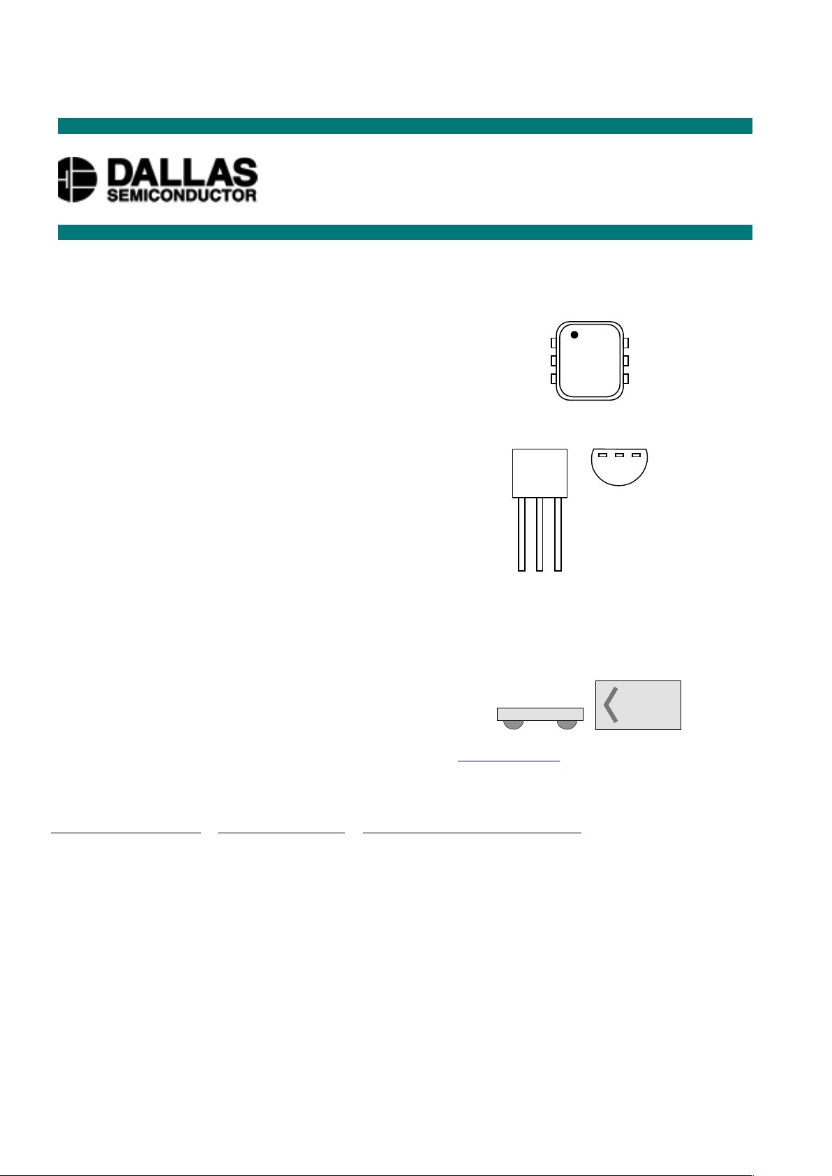
PIN ASSIGNMENT
Top View
6-pin TSOC
1-WIRE
GND
VDD
1
2
3
6
5
4
RH
WIPER
RL
TO-92 Package
123
GND
1-WIRE
RH
123
Bottom View
Flip Chip Package
side view
top view
Visit www.dalsemi.com for Flip Chip pinout and
mechanical data.
ORDERING INFORMATION
PART NUMBER RESISTANCE
*
PACKAGE DESCRIPTION
DS2890-000
100 kΩ
T0-92
DS2890P-000
100 kΩ
6-pin TSOC
DS2890X-000
100 kΩ
Flip Chip Pkg., Tape & Reel
DS2890T-000
100 kΩ
Tape & Reel of DS2890
DS2890V-000
100 kΩ
Tape & Reel of DS2890P
* Contact the factory for availability of alternate resistance values
www.dalsemi.com
PRELIMINARY
DS2890
1-Wire
®
Digital Potentiomete
r
Page 2

DS2890
2 of 27
PIN DESCRIPTION
SIGNAL
NAME TYPE FUNCTION
1-WIRE I/O 1-Wire bus interface. Open drain, requires external pull-up resistor. Range:
2.8V – 6.0V. See HARDWARE CONFIGURATION for pull-up resistor
recommendations.
RH
I/O High end terminal of potentiometer resistor element. Range: 0V – 11.0V.
Range independent of 1-Wire or VDD supply levels as well as the voltage
levels applied to the other potentiometer terminals.
RL
I/O Low end terminal of potentiometer resistor element. Range: 0V – 11.0V.
Range independent of 1-Wire or V
DD
supply levels as well as the voltage
levels applied to the other potentiometer terminals.
WIPER
I/O Potentiometer wiper terminal. Range 0V – 11.0V. Range independent of
1-Wire or VDD supply levels as well as the voltage levels applied to the other
potentiometer terminals.
V
DD
PWR Auxiliary power supply input. Range: 2.8V – 6.0V
GND
PWR Ground
DESCRIPTION
The DS2890 is a linear taper digitally controlled potentiometer with 256 wiper positions. Device
operation, including wiper position, is controlled over the single contact 1-Wire bus for the ultimate in
electrical interface simplicity. With a wide 0–11 volt working voltage range for the potentiometer
terminals, the DS2890 is ideal for a broad range of industrial and control applications. Potentiometer
terminal voltage is independent of device supply voltage as well as the voltage applied to the other
potentiometer terminals. Communication with the DS2890 follows the standard Dallas Semiconductor
1-Wire protocol and can be accomplished with minimal hardware such as a single port pin of a
microcontroller. Multiple DS2890 devices can reside on a common 1-Wire bus and be operated
independently of each other. Each DS2890 has its own unalterable 64-bit ROM registration number that
is factory lasered into the chip. The registration number guarantees unique identification for absolute
traceability and is used to address the device in a multi-drop 1-Wire Network environment. The DS2890
will respond to a 1-Wire Conditional Search command if the potentiometer wiper is set at the power-on
default position. This feature enables the bus master to easily determine whether a potentiometer has
gone through a power-on reset and needs to be re-configured with a required wiper position setting. The
DS2890 supports two power modes: 1-Wire only mode in which device power is supplied parasitically
from the 1-Wire bus or VDD mode where power is supplied from an external supply; when operating from
VDD mode wiper resistance is reduced.
Page 3
DS2890
3 of 27
OPERATION
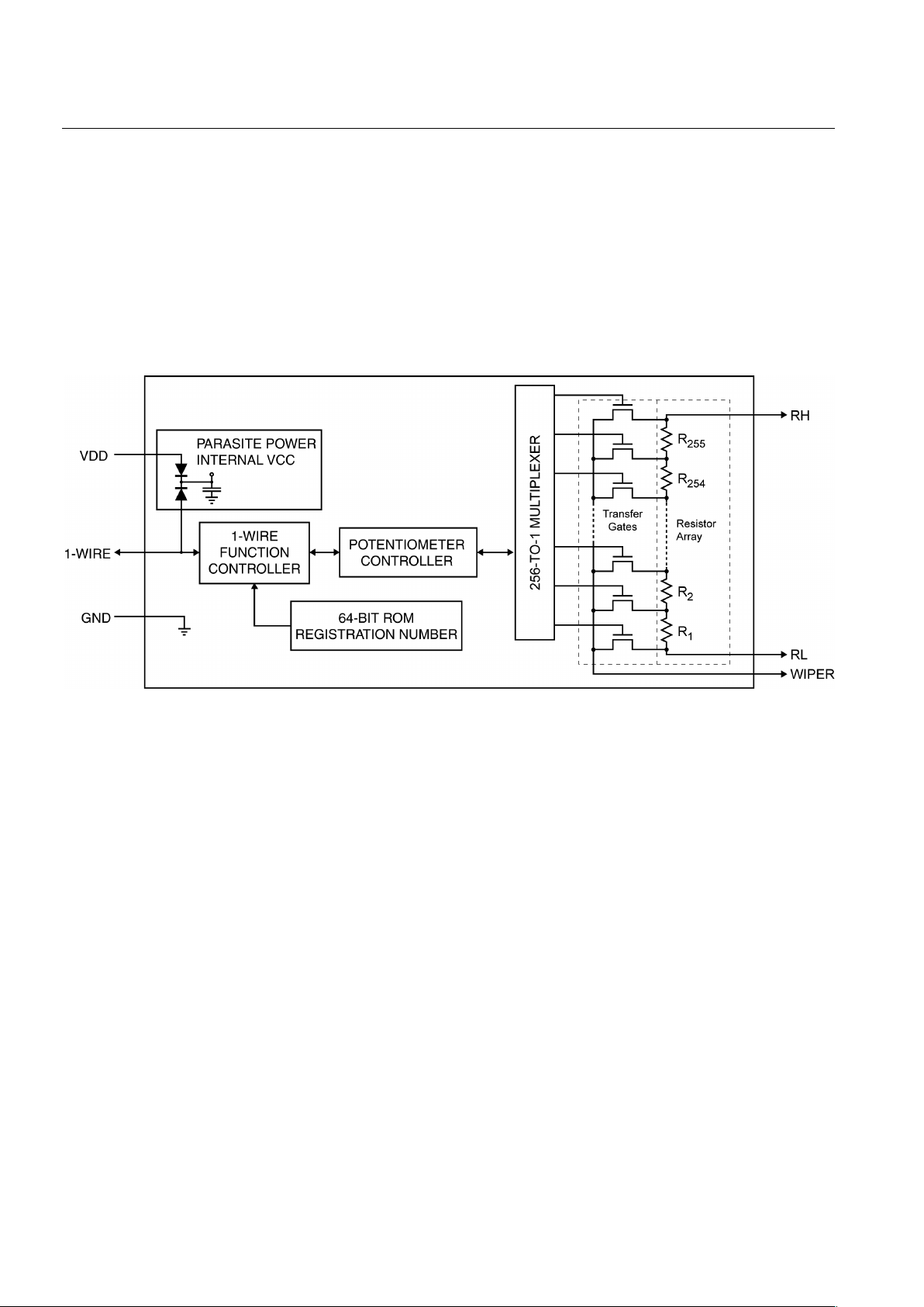
The DS2890 is a single element digital potentiometer; a block diagram of the device is shown in Figure 1.
The device has a total of 256 linearly spaced tap points including the RL and RH terminals; a total of 255
resistive segments exist between the RL and RH terminals. These tap points are ac cessible t o th e W IPER
terminal whose position is controlled via the 1-Wire bus interface. Wiper position and device state are
maintained as long as the 1-Wire bus is active or the V
DD
supply is applied within operating limits.
Otherwise, a power-on reset will occur and the wiper position and operating state will return to power-on
default conditions.
Figure 1. DS2890 BLOCK DIAGRAM
As shown in the figure the device has five major elements: the 1-Wire Function Controller, the
Potentiometer Controller, the 64-bit ROM, the resistor array, and Parasite Power circuitry. Each of these
elements is discussed in detail throughout the remainder of the data sheet. DS2890 control including
device selection, positioning/reading the potentiometer wiper, and device operating state is performed
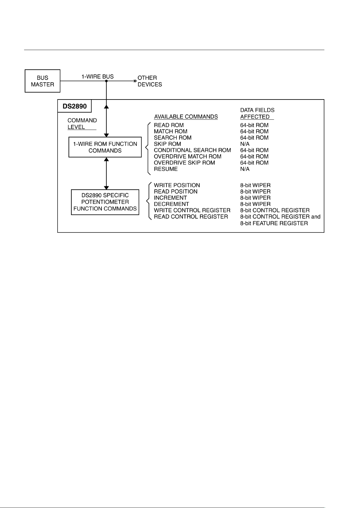
over the 1-Wire bus. The hierarchical structure of the 1-Wire protocol as applicable to the DS2890 is
shown in Figure 2. As shown, the control sequence starts with the 1-Wire bus master issuing one of eight
ROM function commands. After a ROM function command is successfully completed potentiometer
functions may be executed. The protocol for ROM and potentiometer functions are described in the
“COMMAND FLOW” section. For the 3-pin TO-92 package configuration and operation see the
“TO-92 PACKAGE OPERATION” section.
Page 4
DS2890
4 of 27
Figure 2. 1-WIRE COMMAND HIERARCHICAL STRUCTURE
DATA I/O BIT ORDER
All data is read and written least significant bit (LSB) first.
POTENTIOMETER FEATURE REGISTER
Although the feature set of the DS2890 is primarily fixed, a mechanism to identify feature characteristics
of future 1-Wire potentiometers has been developed and implemented in the DS2890. As shown in
Figure 3, the feature register is an encoded read-only byte that describes the cha ract eristics of the DS2890
and future 1-Wire potentiometers. Feature values that correspond to the DS2890 are highlighted. The
feature register is read with the READ CONTROL REGISTER potentiometer function command (see
“POTENTIOMETER FUNCTION COMMANDS”).
Page 5

DS2890
5 of 27
Figure 3. 1-WIRE POTENTIOMETER FEATURE REGISTER
Feature Register Bit Encoding
b7 b6 b5 b4 b3 b2 b1 b0
PR NWP NP WSV PC
Feature Register Bit Definitions
Feature Description Bit(s) Definition
If 0: logarithmic potentiometer element(s)
PC: potentiometer characteristic b0
If 1: linear potentiometer element(s)
If 0: wiper setting(s) are non-volatile
WSV: wiper setting volatility b1
If 1: wiper setting(s) are volatile
NP: number of potentiometers b3..b2 2 bit binary value representing number of potentiometers:
If 00b: 1 potentiometer
If 01b: 2 potentiometers
If 10b: 3 potentiometers
If 11b: 4 potentiometers
NWP: number of wiper positions b5..b4
2 bit binary value representing number of wiper positions
for each potentiometer:
If 00b: 32 positions
If 01b: 64 positions
If 10b: 128 positions
If 11b: 256 positions
PR: potentiometer resistance b7..b6 2 bit binary value representing potentiometer resistance:
If 00b: 5 kΩ
If 01b: 10 kΩ
If 10b: 50 kΩ
If 11b: 100 kΩ
DS2890 feature values are highlighted: value
The DS2890 will respond with a feature register value of F3h when a READ CONTROL
REGISTER command is executed, see section “POTENTIOMETER FUNCTION COMMANDS”.
POTENTIOMETER CONTROL REGISTER
The potentiometer control register is used to turn on/off the DS2890 charge pump (see section
“POTENTIOMETER WIPER RESISTANCE AND CHARGE PUMP CONSIDERATIONS” for a
discussion of the charge pump) and has control capabilities for future 1-Wire potentiometers that could
contain multiple resistor elements. The format of the control register is shown in Figure 4.
Page 6

DS2890
6 of 27
Figure 4. POTENTIOMETER CONTROL REGISTER
Control Register Bit Encoding
b7 b6 b5 b4 b3 b2 b1 b0
XCPC X X
WN
WN
Control Register Bit Definitions*
Description Bit(s) Definition
WN: wiper number to control b1..b0
2 bit binary value representing the potentiometer wiper to
control:
If 00b: potentiometer 1 wiper
If 01b: potentiometer 2 wiper
If 10b: potentiometer 3 wiper
If 11b: potentiometer 4 wiper
WN: inverted wiper number to
control
b3..b2
1’s complement of potentiometer wiper to control:
If 11b: potentiometer 1 wiper
If 10b: potentiometer 2 wiper
If 01b: potentiometer 3 wiper
If 00b: potentiometer 4 wiper
If 0: the charge pump is OFF
CPC: charge pump control b6
If 1: the charge pump is ON
X: don’t care. b4,b5,b7
These bits are reserved for future use by Dallas
Semiconductor. These bits should be written to a value of
0.
*NOTE:
Control Register power-on defaults: Charge Pump is OFF (CPC=0), Wiper Number to control is wiper #1
(WN=00b,
WN=11b).
Valid DS2890 control values are highlighted:
value
Thus for the DS2890, valid control register values are:
Control Register Value Description
00001100b charge pump off, potentiometer #1 wiper selected
01001100b charge pump on, potentiometer #1 wiper selected
As shown in Figure 17 and discussed in the “POTENTIOMETER FUNCTION COMMANDS” section,
no change in device state will occur if an invalid control register value is sent.
Page 7
DS2890
7 of 27
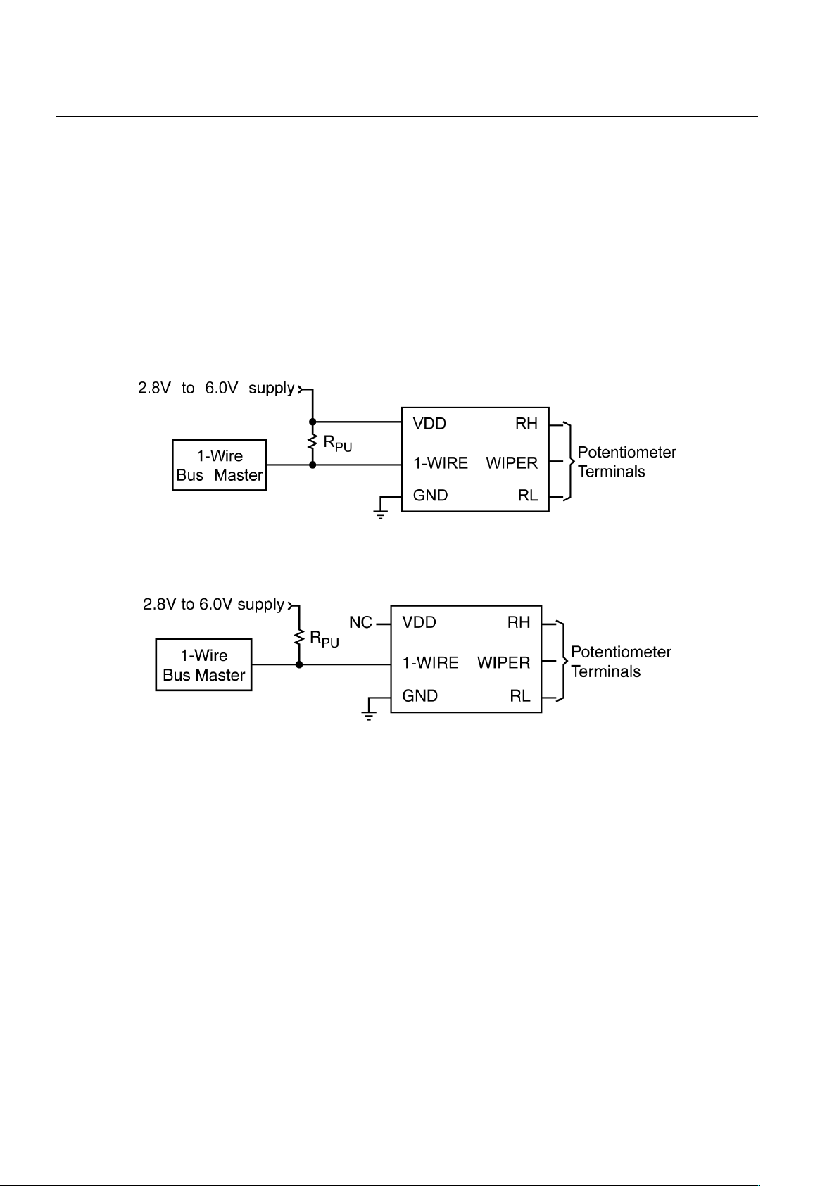
POWER
With the charge pump off, the DS2890 can derive its power entirely from the 1-Wire bus by storing
energy on an internal capacitor during periods of time when the 1-Wire bus is in a high state. During bus
low times the device continues to operate from the energy stored on the internal capacitor; the capacitor is
then recharged when the bus returns to a hi gh state. This t echniqu e of operatin g entirel y from the 1-W ire
bus by powering from energy stored on an internal capacitor during bus low times in known as “parasite
powered” operation. As an option, an auxiliary power source may be connected to the V
DD
power pin.
The auxiliary power mode is appropriate for applications where device charge pump activation is
necessary, the device may be temporarily disconnected from the 1-Wire bus, or bus low times may be
very long. See Figure 5 for example configurations for both power modes.
Figure 5. POWER SUPPLY CONFIGURATION OPTIONS
(a) Auxiliary VDD Supply Configuration
(b) 1-Wire Parasite Power Configuration
POTENTIOMETER WIPER RESISTANCE AND CHARGE PUMP
CONSIDERATIONS
A simplified diagram of the DS2890 resistor array is shown in Figure 6. In this figure the rDS resistance
of the wiper transistors in Figure 1 are modeled as wiper resistance R
WIPER
. The value of R
WIPER
varies
with device configuration, operational state, and wiper terminal voltage. If an auxiliary external V
DD
supply configuration is used as shown In Figure 5a, the DS2890 charge pump may be enabled to reduce
potentiometer wiper resistance. A consequence of enabling the charge pump is increased device power
consumption. This increase is beyond the level that can be supported when operating in 1-Wire parasite
power mode (see POWER section). Therefore if it is necessary to enable the charge pump in an
application, the power supply configuration as shown in Figure 5a must be used. Figure 7 and Figure 8
are graphs of wiper resistance with the charge pump turned ON and OFF respectively.
Page 8
DS2890
8 of 27
Figure 6. POTENTIOMETER RESISTOR MODEL
Figure 7. TYPICAL WIPER RESISTANCE VS WIPER VOLTAGE,
CHARGE PUMP ON
100
1000
10000
0.1 5.5 11
Wiper Volt age ( V)
Wiper Resistance (ohms)
25C
85C
Page 9
DS2890
9 of 27
Figure 8. TYPICAL WIPER RESISTANCE VS WIPER VOLTAGE,
CHARGE PUMP OFF
100
1000
10000
100000
0.1 5.5 11
Wiper Voltage (V)
3V, 25C
3V, 85C
5V, 25C
5v, 85C
TO-92 PACKAGE OPERATION
When packaged in a 3-pin TO-92, the DS2890 takes on a configuration as shown in Figure 9. As shown,
the RL and Wiper terminals and are conn ected to GND and the resistance between the RH terminal and
GND is varied. Note that the DS2890 charge pump must be turned off (default state) for this
configuration. (This is a power consumption issue as described in the section “POTENTIOMETER
WIPER RESISTANCE AND CHARGE PUMP CONSIDERATIONS”.)
Page 10

DS2890
10 of 27
Figure 9. DS2890 TO-92 CONFIGURATION BLOCK DIAGRAM
64-BIT LASTERED ROM
Each DS2890 contains a unique ROM registration number that is 64 bits long; the format of this value is
shown in Figure 10. The first 8 bits are a 1-Wire family code; the family code for the DS2890 and future
1-Wire Potentiometers is 2Ch.. The next 48 bits are a unique serial number that is administered by Dallas
Semiconductor. The last 8 bits are a CRC of the first 56 bits. The 1-Wire CRC is generated using a
polynomial generator consisting of a shift register and XOR gates as shown in Figure 11. Operationally,
the CRC generator works as follows: The shift register bits are first initialized to zero. Then starting with
the least significant bit, the 8-bit family code is shifted in. After the 8th bit of the family code has been
entered, the 48-bit serial number is shifted in. After shifting in the 48th bit of the serial number the shift
register contains the CRC value. Shifting in the 8 bits of CRC should return the shift register to an all
zeros value. Detailed information about the Dallas 1-Wire Cyclic Redundancy Check is available in the
Book of DS19xx iButton Standards. The 64-bit ROM and the 1-Wire Function Controller portions of the
DS2890 allow the device to operate as a 1-Wire device and follow the protocol detailed in the section
“TRANSACTION SEQUENCE”.
Figure 10. 64-BIT LASERED ROM
MSB LSB
8-Bit CRC Code 48-Bit Serial Number 8-Bit Family Code (2Ch)
MSB LSB MSB LSB MSB LSB
Page 11

DS2890
11 of 27
Figure 11. 1-WIRE CRC GENERATOR
R
X
2
X
1
X
0
X
8
X
7
X
6
X
5
X
4
X
3
8TH
STAGE
7TH
STAGE
6TH
STAGE
5TH
STAGE
4TH
STAGE
3RD
STAGE
2ND
STAGE
1ST
STAGE
S
INPUT DATA
Polynomial = X8 + X5 + X4 + 1
POTENTIOMETER FUNCTION COMMANDS
Once the bus master has completed a ROM command sequence, one of six DS2890 potentiometer
function commands can be issued. The Potentiometer Function Command flow charts, Figure 16 and
Figure 17, describe the protocols necessary for adjusting or reading the potentiometer wiper position or
controlling the operating state of the DS2890. All potentiometer functions consist of a single command
byte followed by one or more bytes of data or control written/read by the bus master. All data transferred
between the DS2890 and the bus master are communicated least significant bit first.
READ POSITION [F0H]
The Read Position command is used to obtain the wiper setting of the potentiometer currently addressed
by the Control Register. Although the DS2890 is a single element potentiometer, wiper addressing still
applies and the Control Register wiper number used for addressing must be set accordingly. In addition
to wiper position, the Control Register byte will be returned with a Read Position command. This enables
the bus master to easily confirm/determine the currently addressed potentiometer wiper. Following the
Read Position command byte, the bus master reads 16 bits to obtain first the Control Register byte then
the wiper position byte. The DS2890 will respond with 0’s to additional reads after the 8 bit of the
position byte. The Read Position command is terminated with a Reset pulse.
WRITE POSITION [0FH]
The Write Position command is used to set the position of the currently addressed potentiometer wiper.
Although the DS2890 is a single element potentiometer, wiper addressing still applies and the Control
Register wiper number used for addressin g must be set accordingly. The bus master follows the Write
Position command byte with an 8-bit wiper position value. Following the 8th bit of the position byte, the
bus master reads back the 8-bit position value from the DS2890 to confirm that the value was received
correctly by the device. If an incorrect value is read b ack, the bus master must issue a Reset pulse and
repeat the sequence. If the value read back is correct, the bus master then s ends the 8-bit release code
(96h). If the DS2890 accurately receives the release code, the wiper position is updated and the device
will respond with 0’s to additional reads by the bus master. If an invalid release code is received, no
change is made to the wiper position and the device will respond with 1’s to additional reads by the bus
master. The Write Position command is terminated with a Reset pulse.
Page 12

DS2890
12 of 27
READ CONTROL REGISTER [AAH]
The Read Control Register command is used to obtain both the Control Register and potentiometer
Feature Register. Following the Read Control Register command byte, the bus master reads 16 bits to
obtain first the Feature Register byte and then the Control Register byte. The DS2890 will respond with
0’s to additional reads after the 8 bit of the Control Register byte. The Read Control Register command
is terminated with a Reset pulse.
WRITE CONTROL REGISTER [55H]
The Write Control Register command is used to manipulate DS2890 state bits located in the Control
Register. This command is used to set the potentiometer wiper address and charge pump state. The bus
master follows the Write Control Register command byte with an 8-bit register value. Following the 8th
bit of the register byte, the bus master reads back the 8-bit control value from the DS2890 to confirm that
the device received the correct value (Note that if an invalid register value was received b y the DS2890,
the bus master will read all 1’s (FFh) during the read back sequence.). If a value other than FFh is read,
the bus master determines if the DS2890 received the correct value. If an incorrect value is read back, the
bus master must issue a Reset pulse and repeat the sequence. If the value read back is correct , the bus
master then sends the 8-bit release code (96h). If the DS2890 accuratel y receives the release code, the
Control Register is updated and the device will respond with 0’s to additional reads by the bus master. If
an invalid release code is received, no change is made to the Control Register and the device will respond
with 1’s to additional reads by the bus master. The Write Control Register command is terminated with a
Reset pulse.
INCREMENT [C3H]
The Increment command is used for a one step position increase of the currently addressed potenti ometer
wiper. Although the DS2890 is a single element potentiometer, wiper addressing still applies and the
Control Register wiper number used for addressing must be set accordingly. The bus master follows the
Increment command byte with an 8-bit read to which the DS2890 will respond with the new 8-bit wiper
position set point. No position change is made if the DS2890 wiper is at the maximum position (FFh)
and an Increment command is received. One di fference between the Increment/Decrement commands
and other potentiometer functions is that upon completion of either of these commands, 1-Wi re command
processing remains at the potentiometer function level. As shown in Figure 16, additional potentiometer
commands may be sent without going through the ROM function flow.
DECREMENT [99H]
The Decrement command is used for a one step position decrease of the currently addressed
potentiometer wiper. Although the DS2890 is a single element potentiometer, wiper addressing still
applies and the Control Register wiper number used for addressing must be set accordingly. The bus
master follows the Decrement command byte with an 8-bit read to which the DS2890 will respond with
the new 8-bit wiper position set point. No position change is made if the DS2890 wiper is at the
minimum position (00h) and a Decrement command is received. One difference between the
Increment/Decrement commands and other potentiometer functions is that upon completion of either of
these commands, 1-Wire command processing remains at the potentiometer function level. As shown in
Figure 16, additional potentiometer commands may be sent without going through the ROM function
flow.
Page 13

DS2890
13 of 27
1-WIRE BUS SYSTEM
The 1-Wire bus is a system, which has a single bus master and one or more slaves. In all instances the
DS2890 is a slave device. The bus master is typically a microcontroller. The discussion of this bus system
is broken down into three topics: hardware configuration, transaction sequence, and 1-Wire signaling
(signal types and timing). The 1-Wire protocol defines bus transactions in terms of the bus state during
specific time slots that are initiated on the falling edge of sync pulses from the bus master. For a more
detailed protocol description, refer to Chapter 4 of the Book of DS19xx iButton Standards.
HARDWARE CONFIGURATION
The 1-Wire bus has only a single line by definition; it is important th at each device on the bus be able to
drive it at the appropriate time. To facilitate this, each device attached to the 1-W ire bus must hav e open
drain or 3-state outputs. The 1-Wire port of the DS2890 is open drain with an internal circuit equivalent
to that shown in Figure 9. A multi-drop bus consists of a 1-Wire bus with multiple slaves attached. At
regular speed the 1-Wire bus has a maximum data rate of 16.3 kbits per second. The speed can be boosted
to 142 kbits per second by activating the Overdrive Mode. For a discrete bus master interface as in
Figure 12, the 1-Wire bus requires a pull-up resistor with a minimum value of 2.2 k
Ω. Depending on
1-Wire communication speed, regular or overdrive, and bus load characteristics, the optimal pull-up
resistor value will be in the 1.5 k
Ω to 5 kΩ range. Figure 13 shows a DS2480B bus master configuration
with an interface to the host CPU serial port. Among many features, the DS2480B simplifies the 1-Wire
interface design, generates slew-rate controlled 1-Wire waveforms, and off-loads 1-Wire timing
generation overhead required in a discrete solution.
The idle state for the 1-Wire bus is high. If for any reason a transaction needs to be suspended, the bus
MUST be left in the idle state if the transaction is to resume. If this does not occur and the bus is left low
for more than 16 µs (Overdrive Speed) or more than 120 µs (regular speed), one or more d evices on the
bus may be reset.
Figure 12. HARDWARE CONFIGURATION
RX
TX
Open Drain
Port Pin
5 µA
Typ.
DS2890 1-WIRE PORT
RX = RECEIVE
TX = TRANSMIT
BUS MASTER
V
PUP
DATA
RX
TX
MOSFET
100 Ω
See
Text
NOTE:
Depending on 1-Wire communication speed, regular or overdrive, and bus load characteristics, the
optimal pull-up resistor value will be in the 1.5 k
Ω to 5 kΩ range.
Page 14

DS2890
14 of 27
Figure 13. BUS MASTER WITH DS2480B DRIVER
VDD
POL
RXD
TXD
VPP
1-W
GND
NC
DS2480B
+5V
to 1-WIRE connection
of DS2890
serial in
serial out
HOST CPU
serial
port
BUS MASTER
TRANSACTION SEQUENCE
The protocol for accessing the DS2890 via the 1-Wire port is as follows:
• Initialization
• ROM Function Command
• Potentiometer Function Command
• Transaction/Data
INITIALIZATION
All transactions on the 1-Wire bus begin with an initialization sequence. The initialization sequence
consists of a reset pulse transmitted by the bus master followed by presence pulse(s) transmitted by the
slave(s). The presence pulse lets the bus master know that the DS2890 is on the bus and is ready to
operate. For more details, see the “1 -WIRE SIGNALING” section.
ROM FUNCTION COMM ANDS
Once the bus master has detected a presence, it can issue one of the ei ght ROM function commands that
the DS2890 supports. All ROM function commands are 8 bits long. A list of these commands follows
(refer to Figure 18 and Figure 19 flowcharts):
READ ROM [33H]
This command allows the bus master to read the DS2890’s 8-bit family code, unique 48-bit serial
number, and 8-bit CRC. This command should only be used if there is a single slave on the bus. If more
than one slave is present on the bus, a data collision will occur when all slaves try to transmit at the same
time (open drain will produce a wired-AND result). The resultant family code and 48-bit serial number
read by the master will be invalid.
MATCH ROM [55H]
The match ROM command, followed by a 64-bit ROM sequence, allows the bus master to address a
specific DS2890 on a multi-drop bus. Only the DS2890 that exactly matches the 64-bit ROM sequence
will respond to the following memory function command. All slaves that do not match the 64-bit ROM
sequence will wait for a reset pulse. This command can be used with a single or multiple devices on the
bus.
Page 15

DS2890
15 of 27
SEARCH ROM [F0H]
When a multi-drop system is initially brought up, the bus master might not know the number of devices
on the 1-Wire bus or their 64-bit ROM codes. The search ROM command allows the bus master to use a
process of elimination to identify the 64-bit ROM codes of all slave devices on the bus. The search ROM
process is the repetition of a simple 3-step routine: read a bit, read the complement of the bit, then write
the desired value of that bit. The bus master performs this 3-step routine on each bit of the ROM. After
one complete pass, the bus master knows the 64-bit ROM code of one device. Additional passes will
identify the ROM codes of the remaining devices. See Chapter 5 of the Book of DS19xx iButton
Standards for a comprehensive discussion of a search ROM, including an actual example.
CONDITIONAL SEARCH ROM [ECH]
The Conditional Search ROM command operates similarly to the Search ROM command except that only
devices fulfilling the specified search condition will participate in the search. The device condition that
will cause individual DS2890s to participate in a Conditional Search is a wiper position located at the
power-on default setting (00h). This feature enables the bus master to easily determine whether a
potentiometer has gone through a power-on reset and needs to be re-configured with a required wiper
position setting.
SKIP ROM [CCH]
This command can save time in a single drop bus system by allowing the bus master to access
potentiometer functions without providing the 64-bit ROM code. If more than one slave is present on the
bus and, for example, a read command is issued following the Skip ROM command, data collision will
occur on the bus as multiple slaves transmit simultaneously (open drain pull-downs will produce a wiredAND result).
OVERDRIVE SKIP ROM [3CH]
On a single-drop bus this command can save time by allowing the bus master to access the memory
functions without providing the 64-bit ROM code. Unlike the normal Skip ROM command the
Overdrive Skip ROM sets the DS2890 in the Overdrive Mode. All communication following this
command code has to occur at Overdrive Speed until a reset pulse of minimum 480 µs duration resets all
devices on the bus to regular speed.
When issued on a multi-drop bus this command will set all Overdrive-supporting devices into Overdrive
mode. To subsequently address a specific Overdrive-supporting device, a reset pulse at Overdrive speed
has to be issued followed by a Match ROM or Search ROM command sequence. This will speed up the
search process. If more than one Overdrive-supporting slave is present on the bus and the Ov erdriv e Skip
ROM command is followed by a read command, data collision will occur on the bus as multiple slaves
transmit simultaneously (open drain pull-downs will produce a wire-AND result).
OVERDRIVE MATCH ROM [69H]
The Overdrive Match ROM command, followed by a 64-bit ROM sequence transmitted at Overdrive
Speed, allows the bus master to address a specific DS2890 on a multi-drop bus and to simultaneously set
it in Overdrive Mode. Only the DS2890 that exactly matches the 64-bit ROM sequence will respond to
the subsequent potentiometer function command. Slaves already in Overdrive mode from a previous
Overdrive Skip or a successful Overdrive Match command will remain in Overdrive mode. All Overdrive-capable slaves will return to regular speed at the next Reset Pulse of minimum 480 µs duration. The
Overdrive Match ROM command can be used with a single or multiple devices on the bus.
Page 16

DS2890
16 of 27
RESUME COMMAND [A5H]
In a typical application the DS2890 may be accessed several times to complete a control adjustment. In a
multi-drop environment this means that the 64-bit ROM sequence of a Match ROM command has to be
repeated for every access. To maximize the data throughput in a multi-drop environment the Resume
Command function was implemented. As shown in Figure 19, this function checks the status of the RC
flag and, if it is set, directly transfers control to the potentiometer functions, similar to a Skip ROM
command. The only way to set the RC flag is through successfully executing the Match ROM, Search
ROM, Conditional Search ROM, or Overdrive Match ROM command. Once the RC flag is set, the
device can repeatedly be accessed through the Resume Command function. Accessing another device on
the bus will clear the RC flag, preventing two or more devices from simultaneously responding to the
Resume Command function.
POTENTIOMETER FUNCTION EXAMPLE
At regular speed with an auxiliary supply (VDD within range): turn on the charge pump, set the wiper
position to mid-point, increment the wiper twice, and decrement the wiper once.
MASTER MODE DATA (LSB FIRST) COMMENTS
TX Reset
Reset Pulse (480 - 960
µs)
RX Presence Presence Pulse
TX CCh Issue Skip ROM Command
TX 55h Issue Write Control Register Command
TX 4Ch Issue Control Register value f or WN =0, CPC=1
RX <data byte> Read back Control Register value (4Ch) and verify
TX 96h Issue Release Code to update Control Register
RX <data bits>
If 0’s are read, update was successful; if 1’s are read,
the update failed
TX Reset
Reset Pulse (480 - 960
µs)
RX Presence Presence Pulse
TX CCh Issue Skip ROM Command
TX 0Fh Issue Write Position Command
TX 7Fh Write Wiper Position value
RX <data byte> Read back Wiper Position byte and verify
TX 96h Issue Release Code to update Wiper Position
RX <data bits>
If 0’s are read, update was successful; if 1’s are read,
the update failed
TX Reset Reset Pulse
RX Presence Presence Pulse
TX CCh Issue Skip ROM Command
Page 17

DS2890
17 of 27
MASTER MODE DATA (LSB FIRST) COMMENTS
TX C3h Issue Wiper Increment Command
RX <data byte> Read new wiper position
TX C3h Issue Wiper Increment Command
RX <data byte> Read new wiper position
TX 99h Issue Wiper Decrement Command
RX <data byte> Read new wiper position
TX Reset Reset Pulse
1-WIRE SIGNALING
The DS2890 requires strict protocols to ensure data integrity. The protocol consists of four types of
signaling on one line: Reset Sequence with Reset Pulse and Presence Pulse, Write 0, Write 1 and Read
Data. Except for the presence pulse the bus master initiates all these signals. The DS2890 can
communicate at two different speeds, regular speed and Overdrive Speed. If not explicitly set into the
Overdrive mode, the DS2890 will communicate at regular speed. While in Overdrive Mode the fast
timing applies to all waveforms.
The initialization sequence required to begin any communication with the DS2890 is shown in
Figure 14. A Reset Pulse followed by a Presence Pulse indicates the DS2890 is ready to send or receive
data. The bus master transmits (TX) a reset pulse (t
RSTL
, minimum 480 µs at regular speed, 48 µs at
Overdrive Speed). The bus master then releases the line and go es into receive mode (RX). The 1-Wire
bus is pulled to a high state via the pull-up resistor. After detecting the rising edge on the data contact, the
DS2890 waits (t
PDH
, 15-60 µs at regular speed, 2-6 µs at Overdrive speed) and then transmits the
Presence Pulse (t
PDL
, 60-240 µs at regular speed, 8-24 µs at Overdrive Speed). A Reset Pulse of 480 µs or
longer will exit the Overdrive Mode returning the device to regular speed. If the DS2890 is in Overdrive
Mode and the Reset Pulse is no longer than 80 µs the device will remain in Overdrive Mode.
READ/WRITE TIME SLOTS
The definitions of write and read time slots are illustrated in Figure 15 (a-c). The master initiates all time
slots by driving the data line low. The falling edge of the data line synchronizes the DS2890 to the master
by triggering an internal timing circuit. During write time slots, the timing circuit determines when the
DS2890 will sample the data line. For a read data time slot, if a “0” is to be transmitted, the timing circuit
determines how long the DS2890 will hold the data line low. If the data bit is a “1”, the DS2890 will not
hold the data line low at all.
Page 18

DS2890
18 of 27
Figure 14. INITIALIZATION PROCEDURE “RESET AND PRESENCE PULSES”
RESISTOR
MASTER
DS2890
MASTER RX "PRESENCE PULSE"
REGULAR SPEED OVERDRIVE SPEED
480 µs ≤ t
RSTL
< ∞*
480 µs ≤ t
RSTH
< ∞**
15 µs ≤ t
PDH
< 60 µs
60 ≤ t
PDL
< 240 µs
48 µs ≤ t
RSTL
< 80 µs
48 µs ≤ t
RSTH
< ∞**
2 µs ≤ t
PDH
< 6 µs
8 ≤ t
PDL
< 24 µs
MASTER TX
"RESET PULSE"
V
PULLUP
V
PULLUP MIN
V
IH MIN
V
IL MAX
0V
t
RSTH
t
RSTL
t
PDH
t
PDL
t
R
* In order not to mask interrupt signaling by other devices on the 1-Wire bus and to pr event a power-
on reset of the parasite powered circuit, t
RSTL
+ tR should always be less than 960 µs.
** Includes recovery time.
Figure 15. READ/WRITE TIMING DIAGRAMS
a) Write-one Time Slot
15µs
(OD: 2µs)
60µs
(OD: 6µs)
DS2890
Sampling Window
V
PULLUP
V
PULLUP MIN
V
IH MIN
V
IL MAX
0V
t
SLOT
t
REC
t
LOW1
REGULAR SPEED OVERDRIVE SPEED
60 µs ≤ t
SLOT
< 120 µs
1 µs ≤ t
LOW1
< 15 µs
6 µs ≤ t
SLOT
< 16 µs
1 µs ≤ t
LOW1
< 2 µs
1 µs ≤ t
REC
<
∞
1 µs ≤ t
REC
<
∞
RESISTOR
MASTER
Page 19

DS2890
19 of 27
b) Write-zero Time Slot
15µs
RESISTOR
MASTER
(OD: 2µs)
DS2890
60µs
t
LOW0
Sampling Window
(OD: 6µs)
REGULAR SPEED
OVERDRIVE SPEED
60 µs ≤ t
LOW0
< t
SLOT
< 120 µs
1 µs ≤ t
REC
<
∞
6 µs ≤ t
LOW0
< t
SLOT
< 16 µs
1 µs ≤ t
REC
<
∞
V
PULLUP
V
PULLUP MIN
V
IH MIN
V
IL MAX
0V
t
SLOT
t
REC
c) Read-data Time Slot
RESISTOR
MASTER
DS2890
Master
Sampling Window
REGULAR SPEED OVERDRIVE SPEED
60 µs ≤ t
SLOT
< 120 µs
1 µs ≤ t
LOWR
< 15 µs
0 ≤ t
RELEASE
< 45 µs
1 µs ≤ t
REC
<
∞
t
RDV
= 15 µs
t
SU
< 1 µs
6 µs ≤ t
SLOT
< 16 µs
1 µs ≤ t
LOWR
< 2 µs
0 ≤ t
RELEASE
< 4 µs
1 µs ≤ t
REC
<
∞
t
RDV
= 2 µs
tSU < 1 µs
V
PULLUP
V
PULLUP MIN
V
IH MIN
V
IL MAX
0V
t
SLOT
t
REC
t
LOWR
t
SU
t
RDV
t
RELEASE
*The optimal sampling point for the master is as close as possible to the end time of the t
RDV
period
without exceeding t
RDV
. For the case of a Read-one time slot, this maximizes the amount of time for the
pull-up resistor to recover the line to a high level. For a Read-zero time slot it ensures that a read will
occur before the fastest 1-Wire device(s) release the line (t
RELEASE
= 0).
Page 20

DS2890
20 of 27
Figure 16. POTENTIOMETER FUNCTION COMMAND FLOW
Page 21

DS2890
21 of 27
Figure 17. POTENTIOMETER FUNCTION COMMAND FLOW (continued)
Page 22

DS2890
22 of 27
Figure 18. ROM FUNCTION COMMAND FLOW
Page 23

DS2890
23 of 27
Figure 19. ROM FUNCTION COMMAND FLOW (continued)
Page 24

DS2890
24 of 27
ELECTRICAL CHARACTERISTICS
ABSOLUTE MAXIMUM RATINGS
Voltage on RH, RL, WIPER Relative to Ground -0.5V to +11.0V
Voltage on Other Pins Relative to Ground -0.5V to +6.0V
Operating Temperature -40
o
C to +85oC
Storage Temperature -55
o
C to +125oC
Soldering Temperature See J-STD-020A specification
* This is a stress rating only and functional operation of the device at these or any other conditions above
those indicated in the operation sections of this specification is not implied. Exposure to absolute
maximum rating conditions for extended periods of time may affect reliability.
RECOMMENDED DC OPERATING CONDITIONS -40°C ≤ TA ≤ +85°C
PARAMETER SYMBOL MIN TYP MAX UNITS NOTES
1-Wire Pull-Up Voltage V
PUP
2.8 6.0 V 1
2.8 6.0 V 1,2
Auxiliary Supply Voltage V
DD
-0.3 0.8 V 1,3
NOTES:
1. Voltages are referenced to ground
2.
Range applicable when an auxiliary V
DD
supply is used
3.
Range applicable when an auxiliary V
DD
supply is not used
POTENTIOMETER CHARACTERISTIC
2.8V ≤ V
PUP
≤ 6.0V, -40°C ≤ TA ≤ +85°C
PARAMETER SYMBOL MIN TYP MAX UNITS NOTES
Resistor Terminal Voltage -0.3 11.0 V 1
End-to-End Total Resistance 100
k
Ω
End-to-End Resistance Tolerance -25 25 % 2
Wiper Resistance: R
WIPER
3
Absolute Linearity
±0.6
LSB 4
Relative Linearity
±0.25
LSB 5
-3 dB cutoff frequency f
CUTOFF
100 kHz
Temperature Coefficient 800 ppm/oC
Page 25

DS2890
25 of 27
NOTES:
1. Voltage is referenced to ground.
2.
Valid at 25
o
C only.
3.
Wiper resistance is a function of operating characteristics. See section “POTENTIOMETER WIPER
RESISTANCE AND CHARGE PUMP CONSIDERATIONS” for R
WIPER
characteristics.
4.
Absolute linearity is a measure of wiper output voltage versus expected wiper voltage as determined
by wiper position.
5.
Relative linearity is a measure of the output deviation between successive potentiometer tap points.
DC ELECTRICAL CHARACTERISTICS
2.8V ≤ V
PUP
≤ 6.0V, -40°C ≤ TA ≤ +85°C
PARAMETER SYMBOL MIN TYP MAX UNITS NOTES
1-Wire Input High V
IH
2.2 V 1
1-Wire Input Low V
IL
-0.3 0.8 V 1,2
1-Wire Output High V
OH
V
PUP
6.0 V 1,3
1-Wire Output Low @ 4 mA V
OL
0.4 V 1
1-Wire Input Leakage Current I
L
5
µA
4
VDD Input Current, Charge Pump
OFF
I
DD
4.0
µA
5
VDD Input Current, charge Pump
ON
I
DD
2.0 mA 6
NOTES:
1. Voltages are referenced to ground.
2.
Under certain low voltage conditions V
ILMAX
may have to be reduced to as much as 0.5V to alw ays
guarantee a presence pulse.
3.
V
PUP
is the external 1-Wire pull-up voltage.
4.
Input load is to ground.
5.
Input current when an auxiliary V
DD
supply is used and the charge pump is turned OFF.
6.
Input current when an auxiliary V
DD
supply is used and the charge pump is turned ON.
Page 26

DS2890
26 of 27
AC ELECTRICAL CHARACTERISTICS - REGULAR 1-WIRE SPEED
2.8V ≤ V
PUP
≤ 6.0V, -40°C ≤ TA ≤ +85°C
PARAMETER SYMBOL MIN TYP MAX UNITS NOTES
Time Slot t
SLOT
60 120 µs
Write 1 Low Time t
LOW1
115µs
Write 0 Low Time t
LOW0
60 120 µs
Read Low Time t
LOWR
115µs
Read Data Valid t
RDV
15 µs 1
Release Time t
RELEASE
01545µs
Read Data Setup t
SU
1µs2
Recovery Time t
REC
1µs
Reset High Time t
RSTH
480 µs 3
Reset Low Time t
RSTL
480 µs 4
Presence Detect High t
PDH
15 60 µs
Presence Detect Low t
PDL
60 240 µs
NOTES:
1. The optimal sampling point for the master is as close as possible to the end time of the 15 µs t
RDV
period without exceeding t
RDV
. For the case of a Read-one time slot, this maximizes the amount of
time for the pull-up resistor to recover the line to a high level. For a Read-zero time slot it ensures
that a read will occur before the fastest 1-Wire device(s) release the line (t
RELEASE
= 0).
2.
Read data setup time refers to the time the host must pull the 1-Wire bus low to read a bit. Data is
guaranteed to be valid within 1 µs of this falling edge.
3.
An additional reset or communication sequence cannot begin until the reset high time (t
RSTH
) has
expired.
4.
The reset low time (t
RSTL
) should be restricted to a maximum of 960 µs, to allow interrupt signaling,
otherwise, it could mask or conceal interrupt pulses.
AC ELECTRICAL CHARACTERISTICS - OVERDRIVE 1-WIRE SPEED
2.8V ≤ V
PUP
≤ 6.0V, -40°C ≤ TA ≤ +85°C
PARAMETER SYMBOL MIN TYP MAX UNITS NOTES
Time Slot t
SLOT
616µs
Write 1 Low Time t
LOW1
12µs
Write 0 Low Time t
LOW0
616µs
Read Low Time t
LOWR
12µs
Read Data Valid t
RDV
2µs9
Release Time t
RELEASE
01.54µs
Read Data Setup t
SU
1µs4
Page 27

DS2890
27 of 27
AC ELECTRICAL CHARACTERISTICS - OVERDRIVE 1-WIRE SPEED
2.8V ≤ V
PUP
≤ 6.0V, -40°C ≤ TA ≤ +85°C
PARAMETER SYMBOL MIN TYP MAX UNITS NOTES
Recovery Time t
REC
1µs
Reset High Time t
RSTH
48 µs
Reset Low Time t
RSTL
48 80 µs
Presence Detect High t
PDH
26µs
Presence Detect Low t
PDL
824µs
NOTES:
1. The optimal sampling point for the master is as close as possible to the end time of the 2 µs t
RDV
period without exceeding t
RDV
. For the case of a Read-one time slot, this maximizes the amount of
time for the pull-up resistor to recover the line to a high level. For a Read-zero time slot it ensures
that a read will occur before the fastest 1-Wire device(s) release the line (t
RELEASE
= 0).
2.
Read data setup time refers to the time the host must pull the 1-Wire bus low to read a bit. Data is
guaranteed to be valid within 1 µs of this falling edge.
3.
An additional reset or communication sequence cannot begin until the reset high time (t
RSTH
) has
expired.
4.
The reset low time (t
RSTL
) should be restricted to a maximum of 960 µs, to allow interrupt signaling,
otherwise, it could mask or conceal interrupt pulses.
CAPACITANCE TA = 25°C
PARAMETER SYMBOL MIN TYP MAX UNITS NOTES
1-Wire Pin 800 pF 1
VDD Pin 10 pF
Resistor Terminals 10 pF
NOTE:
1. Capacitance on the 1-Wire pin could be 800 pF when power is first applied. If a 5 kΩ is used to pull
up the 1-Wire line to V
PUP
, the capacitance will not affect communications after a 5 µs charge time.
 Loading...