

Page 1
DS26S10
Quad Bus Transceiver
General Description
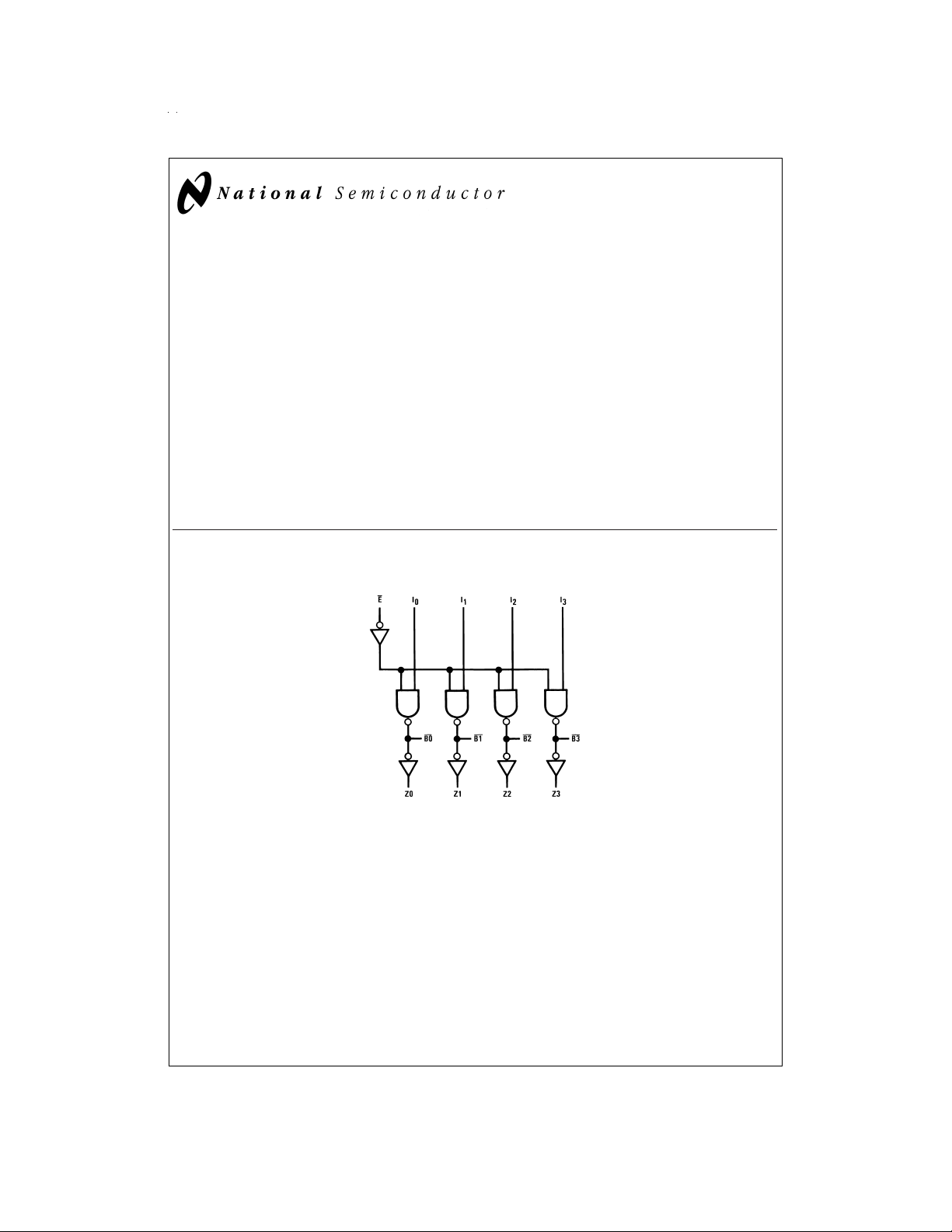
The DS26S10 is a quad Bus Transceiverconsistingof4high
speed bus drivers with open-collector outputs capable of
sinking 100 mA at 0.8V and 4 high speed bus receivers.
Each driver output is connected internally to the high speed
bus receiver in addition to being connected to the package
pin. The receiver has a Schottky TTL output capable of driving 10 Schottky TTL unit loads.
An active low enable gate controls the 4 drivers so that outputs of different device drivers can be connected togetherfor
party-line operation.
The bus output high-drive capability in the low state allows
party-line operation with a line impedance as low as 100Ω.
The line can be terminated at both ends, and still give considerable noise margin at the receiver. The receiver typical
switching point is 2V.
Logic Diagrams
The DS26S10 features advanced Schottky processing to
minimize propagation delay. The device package also has 2
ground pins to improve ground current handling and allow
close decoupling between V
Both GND 1 and GND 2 should be tied to the ground bus external to the device package.
and ground at the package.
CC
Features
n Input to bus is inverting on DS26S10
n Quad high speed open-collector bus transceivers
n Driver outputs can sink 100 mA at 0.8V maximum
n Advanced Schottky processing
n PNP inputs to reduce input loading
DS2610
DS26S10 Quad Bus Transceiver
May 1999
DS005802-1
© 1999 National Semiconductor Corporation DS005802 www.national.com
Page 2
Absolute Maximum Ratings (Note *NO
TARGET FOR FNXref NS859*)
If Military/Aerospace specified devices are required,
please contact the National Semiconductor Sales Office/
Distributors for availability and specifications.
Storage Temperature −65˚C to +150˚C
Temperature (Ambient) Under Bias −55˚C to +125˚C
Supply Voltage to Ground Potential −0.5V to +7V
DC Voltage Applied to Outputs for −0.5V to +V
High Output State
DC Input Voltage −0.5V to +5.5V
Output Current, Into Bus 200 mA
Output Current, Into Outputs
(Except Bus) 30 mA
Max
CC
DC Input Current −30 mA to +5 mA
Maximum Power Dissipation (Note 1) at 25˚C
Molded Package 1362 mW
Operating Conditions
Min Max Units
Supply Voltage (V
DS26S10 4.75 5.25 V
Temperature (T
DS26S10 0 +70 ˚C
Note 1: Derate cavitypackage9.6 mW/˚C above 25˚C; derate molded package 10.9 mW/˚C above 25˚C, derate PLCC package TBD mW/˚C above
25˚C.
)
CC
)
A
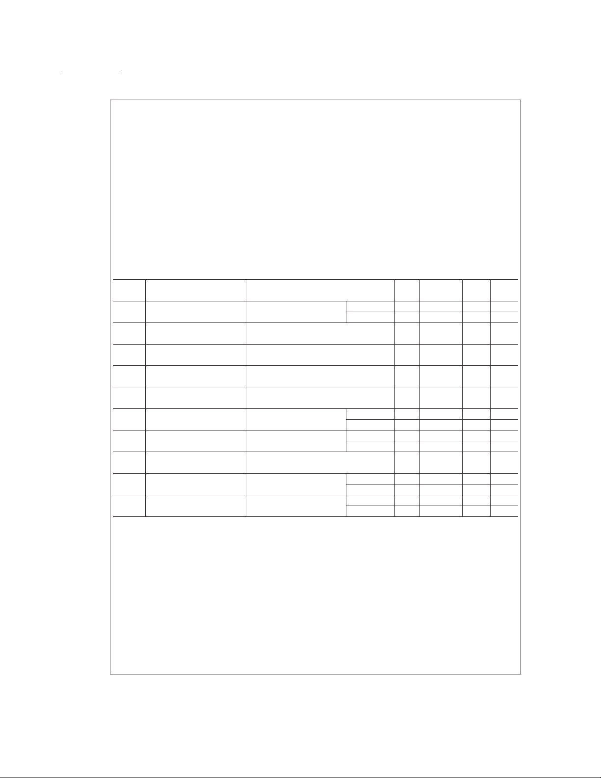
Electrical Characteristics
(Unless otherwise noted)
Symbol Parameter Conditions Min Typ Max Units
(Note 2) (Note 3)
V
OH
Output High Voltage V
(Receiver Outputs) V
V
OL
Output Low Voltage V
(Receiver Outputs) V
V
IH
Input High Level Guaranteed Input Logical High for 2.0 V
=
CC
=
V
IN
=
CC
=
V
IN
(Except Bus) All Inputs
V
IL
Input Low Level Guaranteed Input Logical Low for 0.8 V
(Except Bus) All Inputs
V
I
Input Clamp Voltage V
=
CC
(Except Bus)
I
IL
Input Low Current V
=
CC
(Except Bus) Data −0.54 mA
I
IH
Input High Current V
=
CC
(Except Bus) Data 30 µA
I
I
Input High Current V
=
CC
(Except Bus)
I
SC
Output Short-Circuit Current V
=
CC
(Except Bus) Commercial −18 −60 mA
I
CCL
Power Supply Current V
=
CC
(All Bus Outputs Low) DS26S11 80 mA
=
Min, I
IL
Min, I
IL
Min, I
Max, V
Max, V
Max, V
−1 mA, Military 2.5 3.4 V
OH
or V
IH
=
20 mA, 0.5 V
OL
or V
IH
=
−18 mA −1.2 V
IN
=
0.4V Enable −0.36 mA
IN
=
2.7V Enable 20 µA
IN
=
5.5V 100 µA
IN
Commercial 2.7 3.4 V
Max, (Note 4) Military −20 −55 mA
Max, Enable=GND DS26S10 45 70 mA
www.national.com 2
Page 3
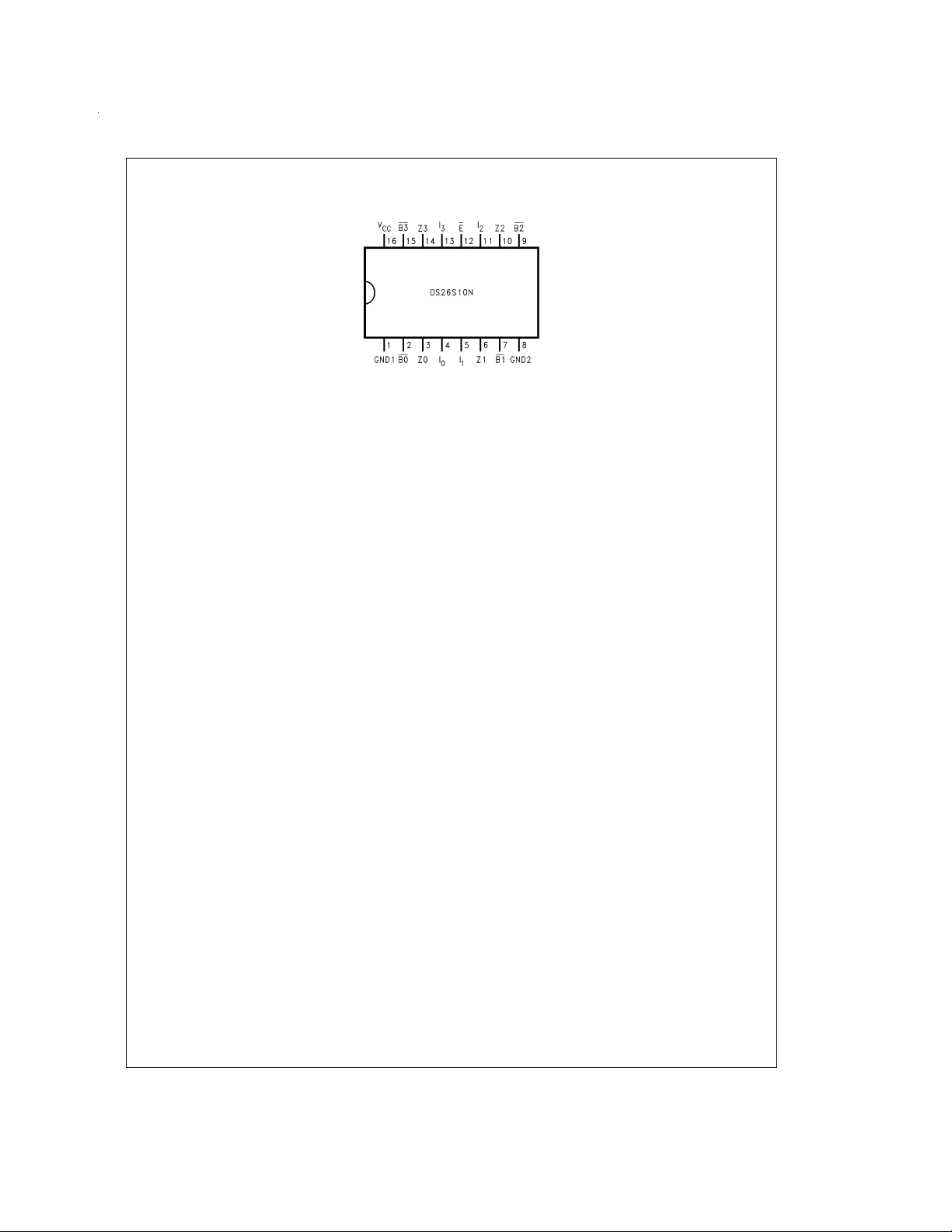
Connection Diagram
Dual-In-Line Package
DS005802-3
Top View
Order Number DS26S10N
See NS Package Number N16A
Plastic Chip Carrier
www.national.com3
Page 4

Bus Input/Output Characteristics
Symbol Parameter Conditions
Min Typ(Note3)Max Units
(Note 2)
V
OL
I
O
I
OFF
V
TH
V
TL
Note 2: For conditions shown as min or max, use the appropriate value specified under Electrical Characteristics for the applicable device type.
Note 3: Typical limits are at V
Note 4: Not more than one output should be shorted at a time. Duration of the short circuit test should not exceed one second.
Output Low Voltage
=
V
Min
CC
Bus Leakage Current
Bus Leakage Currrent (power
OFF)
=
Max
V
CC
=
V
4.5V 100
O
Receiver Input High Threshold Bus enable=2.4V
=
Max
V
CC
Receiver Input Low Threshold Bus enable=2.4V
=
Min
V
CC
=
5V, 25˚C ambient and maximum loading.
CC
=
40 mA 0.33 0.5
I
OL
=
70 mA 0.42 0.05
OL
=
I
100 mA 0.51 0.8
OL
=
V
0.8V −50
O
=
4.5V 100
V
O
2.25 2.0
2.0 1.75
µA
µA
Switching Characteristics
=
(T
25˚C, V
A
Symbol Parameter Conditions Min Typ Max Units
t
PLH
t
PHL
t
PLH
t
PHL
t
PLH
t
PHL
t
r
t
f
Note 5: Includes probe and jig capacitance.
=
5V)
CC
Data Input to Bus R
=
B
Data Input to Bus 10 15 ns
Enable Input to Bus
Enable Input to Bus 13 18 ns
Bus to Receiver Out R
Bus to Receiver Out C
Bus R
=
B
=
L
=
B
=
50Ω,C
50Ω,R
50 pF (Note 5)
B
=
280Ω,C
L
DS26S10
DS26S10
=
50 pF(Note 5) 10 15 ns
B
10 15 ns
14 18 ns
15 pF 10 15 ns
=
50Ω,C
50 pF (Note 5) 4.0 10 ns
B
Bus 2.0 4.0 ns
VI
V
Truth Tables
DS26S10
Inputs Outputs
E
LLHL
LHLH
HXYY
=
H
High voltage level
L=Low voltage level
X=Don’t care
Y=Voltage level of bus (assumes control by another bus transceiver)
www.national.com 4
IBZ
Page 5

Typical Application
AC Test Circuit and Switching Time Waveforms
DS005802-5
Note 1: Includes probe and jig capacitance.
DS005802-6
DS005802-7
www.national.com5
Page 6

Typical Performance Characteristics
Typical Bus Output Low Voltage vs Ambient Temperature
Schematic Diagram
DS005802-8
Receiver Threshold Variation
vs Ambient Temperature
DS005802-9
=
V
Pin 16
CC
GND 1=Pin 1
GND 2=Pin 8
Connect for DS26S10
*Remove R1, Q1, D1 for DS26S10
www.national.com 6
DS005802-10
Page 7

Physical Dimensions inches (millimeters) unless otherwise noted
Molded Dual-In-Line Package (N)
Order Number DS26S10N
NS Package Number N16A
DS26S10 Quad Bus Transceiver
LIFE SUPPORT POLICY
NATIONAL’S PRODUCTS ARE NOT AUTHORIZED FOR USE AS CRITICAL COMPONENTS IN LIFE SUPPORT
DEVICES OR SYSTEMS WITHOUT THE EXPRESS WRITTEN APPROVAL OF THE PRESIDENT AND GENERAL
COUNSEL OF NATIONAL SEMICONDUCTOR CORPORATION. As used herein:
1. Life support devices or systems are devices or
systems which, (a) are intended for surgical implant
into the body, or (b) support or sustain life, and
whose failure to perform when properly used in
accordance with instructions for use provided in the
2. A critical component is any component of a life
support device or system whose failure to perform
can be reasonably expected to cause the failure of
the life support device or system, or to affect its
safety or effectiveness.
labeling, can be reasonably expected to result in a
significant injury to the user.
National Semiconductor
Corporation
Americas
Tel: 1-800-272-9959
Fax: 1-800-737-7018
Email: support@nsc.com
www.national.com
National does not assume any responsibility for use of any circuitry described, no circuit patent licenses are implied and National reserves the right at any time without notice to change said circuitry and specifications.
National Semiconductor
Europe
Fax: +49 (0) 1 80-530 85 86
Email: europe.support@nsc.com
Deutsch Tel: +49 (0) 1 80-530 85 85
English Tel: +49 (0) 1 80-532 78 32
Français Tel: +49 (0) 1 80-532 93 58
Italiano Tel: +49 (0) 1 80-534 16 80
National Semiconductor
Asia Pacific Customer
Response Group
Tel: 65-2544466
Fax: 65-2504466
Email: sea.support@nsc.com
National Semiconductor
Japan Ltd.
Tel: 81-3-5639-7560
Fax: 81-3-5639-7507
 Loading...