

Page 1
DS26LV32AT
3V Enhanced CMOS Quad Differential Line Receiver
General Description
The DS26LV32Ais a high speed quad differential CMOS receiver that meets the requirements of both TIA/EIA-422-B
and ITU-T V.11. The CMOS DS26LV32AT features typical
low static I
CC
of 9 mA which makes it ideal for battery pow-
ered and power conscious applications. The TRI-STATE
®
enables, EN and EN*, allow the device to be active High or
active Low. The enables are common to all four receivers.
The receiver output (RO) is guaranteed to be High when the
inputs are left open. The receiver can detect signals as low
as
±
200 mV over the common mode range of±10V.The receiver outputs (RO) are compatible with TTL and LVCMOS
levels.
Features
n Low Power CMOS design (30 mW typical)
n Interoperable with existing 5V RS-422 networks
n Industrial and Military Temperature Range
n Conforms to TIA/EIA-422-B (RS-422) and ITU-T V.11
Recommendation
n 3.3V Operation
n
±
7V Common Mode Range@VID=3V
n
±
10V Common Mode Range@VID= 0.2V
n Receiver OPEN input failsafe feature
n Guaranteed AC Parameter:
Maximum Receiver Skew: 4 ns
Maximum Transition Time: 10 ns
n Pin compatible with DS26C32AT
n 32 MHz Toggle Frequency
n
>
6.5k ESD Tolerance (HBM)
n Available in SOIC and Cerpack Packaging
n Standard Microcircuit Drawing (SMD) 5962-98585
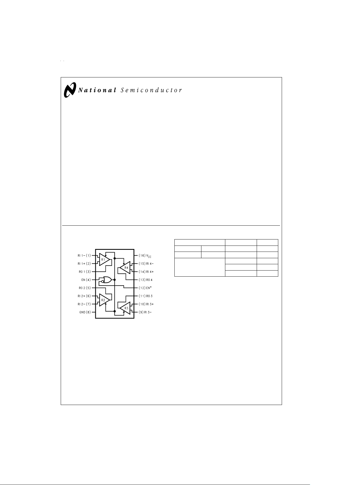
Connection Diagram Truth Table
Enables Inputs Output
EN EN* RI+–RI− RO
LH X Z
All Other V
ID
≥ +0.2V H
Combinations of V
ID
≤ −0.2V L
Enable Inputs Open
†
H
†
Open, not terminated
L = Logic Low
H = Logic High
X = Irrelevant
Z = TRI-STATE
TRI-STATE®is a registered trademark of National Semiconductor Corporation.
Dual-In-Line Package
DS012908-1
Top View
Order Number DS26LV32ATM or DS26LV32AW
See NS Package Number M16A or W16A
April 1999
DS26LV32AT 3V Enhanced CMOS Quad Differential Line Receiver
© 1999 National Semiconductor Corporation DS012908 www.national.com
Page 2
Absolute Maximum Ratings (Note 1)
If Military/Aerospace specified devices are required,
please contact the National Semiconductor Sales Office/
Distributors for availability and specifications.
Supply Voltage (V
CC
) −0.5V to +7V
Enable Input Voltage (EN, EN*) −0.5V to V
CC
+0.5V
Receiver Input Voltage (V
ID
: RI+, RI−)
±
14V
Receiver Input Voltage
(VCM: RI+, RI−)
±
14V
Receiver Output Voltage (RO) −0.5V to V
CC
+0.5V
Receiver Output Current (RO)
±
25 mA Maximum
Maximum Package Power Dissipation
@
+25˚C
M Package 1190 mW
W Package 1087 mW
Derate M Package 9.8 mW/˚C above +25˚C
Derate W Package 7.3 mW/˚C above +25˚C
Storage Temperature Range −65˚C to +150˚C
Lead Temperature Range Soldering
(4 Sec.) +260˚C
ESD Ratings (HBM, 1.5 kΩ, 100 pF)
Receiver Inputs and Enables ≥ 6.5 kV
Other Pins ≥ 2kV
Recommended Operating
Conditions
Min Typ Max Units
Supply Voltage (V
CC
) 3.0 3.3 3.6 V
Operating Free Air Temperature Range (T
A
)
DS26LV32AT −40 +25 +85 ˚C
DS26LV32AW −55 +25 +125 ˚C
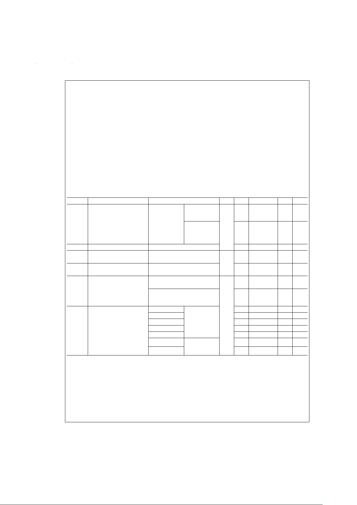
Electrical Characteristics (Notes 2, 3)
Over Supply Voltage and Operating Temperature ranges, unless otherwise specified.
Symbol Parameter Conditions Pin Min Typ Max Units
V
TH
Differential Input Threshold V
OUT=VOH
or
V
OL
VCM= −7V to
+7V, T
A
=
-40˚C to +85˚C
RI+,
RI−
−200
±
17.5 +200 mV
V
CM
= −0.5V to
+5.5V, T
A
=
-55˚C to +125˚C
(Note 9)
-200 +200 mV
V
HY
Hysteresis VCM= 1.5V 35 mV
V
IH
Minimum High Level
EN,
EN*
2.0 V
Input Voltage
V
IL
Maximum Low Level 0.8 V
Input Voltage
R
IN
Input Resistance VIN= −7V, +7V, TA= -40˚C to
+85˚C (Other Input = GND)
RI+,
RI−
5.0 8.5 kΩ
V
IN
= −0.5V, +5.5V, TA= -55˚C to
+125˚C (Other Input = GND) (Note
9)
5.0 kΩ
I
IN
Input Current VIN= +10V TA= -40˚C to
+85˚C
0 1.1 1.8 mA
(Other Input = 0V, V
IN
= +3V 0 0.27 mA
Power On, or V
IN
= 0.5V −0.02 mA
V
CC
= 0V) VIN= −3V 0 −0.43 mA
V
IN
= −10V 0 −1.26 −2.2 mA
V
IN
= −0.5V TA= -55˚C to
+125˚C (Note
9)
0 -1.8 mA
V
IN
= 5.5V 0 1.8 mA
www.national.com 2
Page 3
Electrical Characteristics (Notes 2, 3) (Continued)
Over Supply Voltage and Operating Temperature ranges, unless otherwise specified.
Symbol Parameter Conditions Pin Min Typ Max Units
I
EN
Input Current VIN=0VtoV
CC
EN,
EN*
±
1µA
V
OH
High Level Output Voltage IOH= −6 mA, VID= +1V
RO
2.4 3 V
I
OH
= −6 mA, VID= OPEN
V
OH
High Level Output Voltage IOH= −100 µA, VID= +1V VCC−0.1 V
I
OH
= − 100 µA, VID= OPEN
V
OL
Low Level Output Voltage IOL= +6 mA, VID= −1V 0.13 0.5 V
I
OZ
Output TRI-STATE Leakage V
OUT=VCC
or GND
±
50 µA
Current EN = V
IL
,EN*=V
IH
I
SC
Output Short Circuit Current VO= 0V, VID≥ |200 mV| (Note 4) −10 −35 −70 mA
I
CC
Power Supply Current No Load, All
RI+, R1− =
OPEN, EN,
EN*=V
CC
or
GND
T
A
= -40˚C to
+85˚C
V
CC
915mA
T
A
= -55˚C to
+125˚C
20 mA
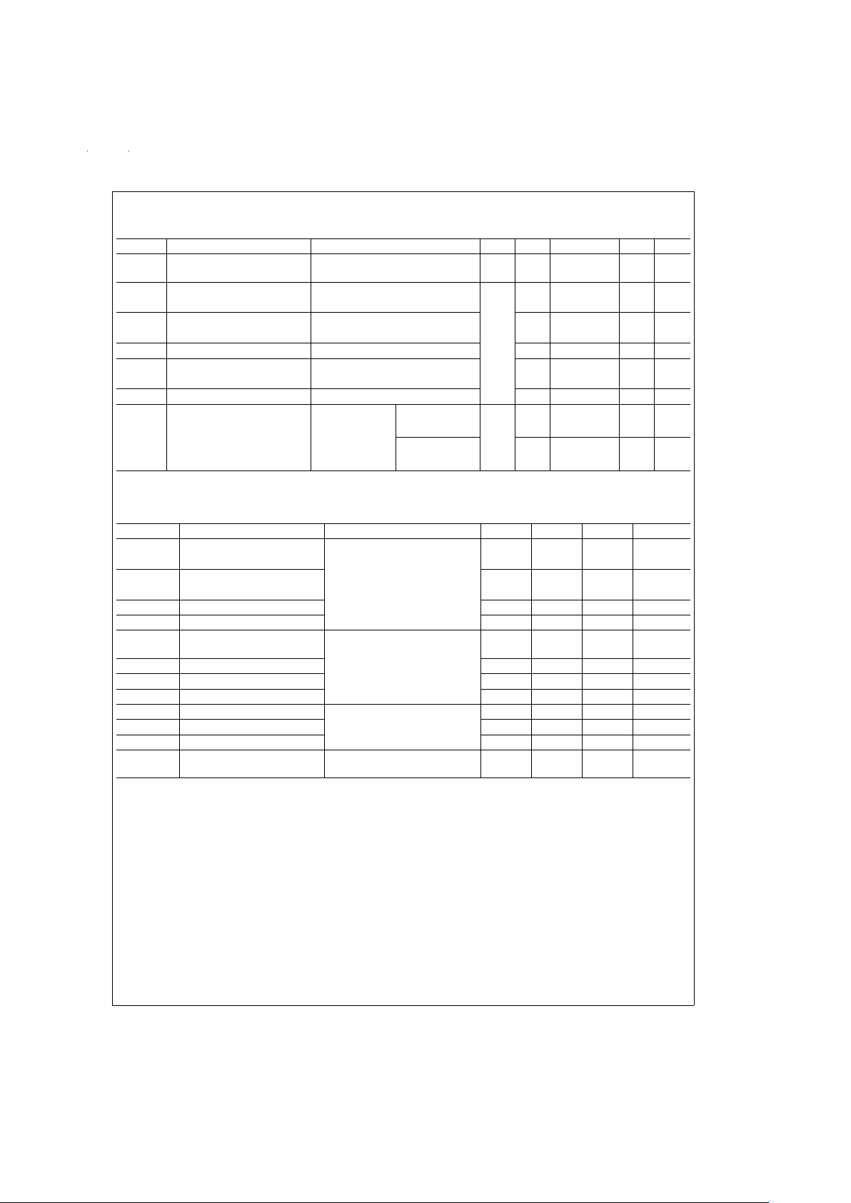
Switching Characteristics - Industrial (Notes 3, 7, 10, 11)
Over Supply Voltage and -40˚C to +85˚C Operating Temperature range, unless otherwise specified.
Symbol Parameter Conditions Min Typ Max Units
t
PHL
Propagation Delay CL= 15 pF, VCM= 1.5V
(
Figures 1, 2
)
6 17.5 35 ns
High to Low
t
PLH
Propagation Delay 6 17.8 35 ns
Low to High
t
r
Rise Time (20%to 80%) 4.1 10 ns
t
f
Fall Time (80%to 20%) 3.3 10 ns
t
PHZ
Disable Time CL= 50 pF, VCM= 1.5V
(
Figures 3, 4
)
40 ns
t
PLZ
Disable Time 40 ns
t
PZH
Enable Time 40 ns
t
PZL
Enable Time 40 ns
t
SK1
Skew, |t
PHL−tPLH
| (Note 5) CL= 15 pF, VCM= 1.5V 0.3 4 ns
t
SK2
Skew, Pin to Pin (Note 6) 0.6 4 ns
t
SK3
Skew, Part to Part (Note 7) 7 17 ns
f
MAX
Maximum Operating
Frequency (Note 8)
CL= 15 pF, VCM= 1.5V 32 MHz
www.national.com3
Page 4

Switching Characteristics - Military (Notes 10, 11)
Over Supply Voltage and -55˚C to +125˚C Operating Temperature range, unless otherwise specified.
Symbol Parameter Conditions Min Max Units
t
PHL
Propagation Delay CL= 50 pF, VCM= 1.5V
(
Figures 1, 2
)
645 ns
High to Low
t
PLH
Propagation Delay 6 45 ns
Low to High
t
PHZ
Disable Time CL= 50 pF, VCM= 1.5V
(
Figures 3, 4
)
50 ns
t
PLZ
Disable Time 50 ns
t
PZH
Enable Time 50 ns
t
PZL
Enable Time 50 ns
t
SK1
Skew, |t
PHL−tPLH
| (Note 5) CL= 50 pF, VCM= 1.5V 6 ns
t
SK2
Skew, Pin to Pin (Note 6) 6 ns
Note 1: “Absolute Maximum ratings” are those values beyond which the safety of the device cannot be guaranteed. They are not meant to imply that the devices
should be operated at these limits. The table of “Electrical Characteristics” specifies conditions of device operation.
Note 2: Current into device pins is defined as positive. Current out of device pins is defined as negative. All voltages are referenced to ground except V
ID
.
Note 3: All typicals are given for: V
CC
= +3.3V,TA= +25˚C.
Note 4: Short one output at a time to ground. Do not exceed package.
Note 5: t
SK1
is the |t
PHL–tPLH
| of a channel.
Note 6: t
SK2
is the maximum skew between any two channels within a device, either edge.
Note 7: t
SK3
is the difference in propagation delay times between any channels of any devices. This specification (maximum limit) applies to devices within V
CC
±
0.1V of one another,and a DeltaT
A
=
±
5˚C (between devices) within the operating temperature range. This parameter is guaranteed by designand characterization.
Note 8: All channels switching, Output Duty Cycle criteria is 40%/60%measured at 50%. Input = 1V to 2V, 50%Duty Cycle, t
r/tf
≤ 5 ns. This parameter is guaranteed
by design and characterization.
Note 9: This parameter does not meet the TIA/EIA-422-B specification.
Parameter Measurement Information
DS012908-2
FIGURE 1. Receiver Propagation Delay and Transition Time Test Circuit (Notes 10, 11)
www.national.com 4
Page 5

Parameter Measurement Information (Continued)
DS012908-3
Note 10: Generator waveform for all tests unless otherwise specified:f=1MHz, Duty Cycle = 50%,ZO=50Ω,tr≤10 ns, tf≤ 10 ns.
Note 11: C
L
includes probe and jig capacitance.
Note 12: For military grade product, t
r
≤ 6ns and tf≤ 6ns.
Note 13: For military grade product the measure point is 1/2 V
CC
for t
PLH,tPHL,tPZL
, and t
PZH
FIGURE 2. Receiver Propagation Delay and Transition Time Waveform (Notes 10, 11, 12, 13)
DS012908-4
FIGURE 3. Receiver TRI-STATE Test Circuit
DS012908-5
FIGURE 4. Receiver TRI-STATE Output Enable and Disable Waveforms (Notes 10, 11, 12, 13)
www.national.com5
Page 6

Typical Application Information
General application guidelines and hints for differential drivers and receivers may be found in the following application
notes:
AN-214,AN-457, AN-805, AN-847,AN-903, AN-912, AN-916
Power Decoupling Recommendations:
Bypass caps must be used on power pins. High frequency
ceramic (surface mount is recommended) 0.1 µF in parallel
with 0.01 µF at the power supply pin. A 10 µF or greater solid
tantalum or electrolytic should be connected at the power
entry point on the printed circuit board.
DS012908-6
RTis optional although highly recommended to reduce reflection
DS012908-7
FIGURE 5. Typical Receiver Connections
DS012908-8
FIGURE 6. Typical Receiver Output Waveforms
DS012908-9
FIGURE 7. Typical Receiver Input Circuit
www.national.com 6
Page 7

Typical Application Information (Continued)
DS012908-10
FIGURE 8. Typical ICCvs Frequency
DS012908-11
FIGURE 9. Receiver IINvs VIN(Power On or Power Off)
DS012908-12
FIGURE 10. IOLvs V
OL
www.national.com7
Page 8

Typical Application Information (Continued)
DS012908-13
FIGURE 11. IOHvs V
OH
www.national.com 8
Page 9

Physical Dimensions inches (millimeters) unless otherwise noted
Order Number DS26LV32ATM
NS Package Number M16A
www.national.com9
Page 10

Physical Dimensions inches (millimeters) unless otherwise noted (Continued)
LIFE SUPPORT POLICY
NATIONAL’S PRODUCTS ARE NOT AUTHORIZED FOR USE AS CRITICAL COMPONENTS IN LIFE SUPPORT
DEVICES OR SYSTEMS WITHOUT THE EXPRESS WRITTEN APPROVAL OF THE PRESIDENT OF NATIONAL
SEMICONDUCTOR CORPORATION. As used herein:
1. Life support devices or systems are devices or
systems which, (a) are intended for surgical implant
into the body, or (b) support or sustain life, and
whose failure to perform when properly used in
accordance with instructions for use provided in the
labeling, can be reasonably expected to result in a
significant injury to the user.
2. A critical component is any component of a life
support device or system whose failure to perform
can be reasonably expected to cause the failure of
the life support device or system, or to affect its
safety or effectiveness.
National Semiconductor
Corporation
Americas
Tel: 1-800-272-9959
Fax: 1-800-737-7018
Email: support@nsc.com
National Semiconductor
Europe
Fax: +49 (0) 1 80-530 85 86
Email: europe.support@nsc.com
Deutsch Tel: +49 (0) 1 80-530 85 85
English Tel: +49 (0) 1 80-532 78 32
Français Tel: +49 (0) 1 80-532 93 58
Italiano Tel: +49 (0) 1 80-534 16 80
National Semiconductor
Asia Pacific Customer
Response Group
Tel: 65-2544466
Fax: 65-2504466
Email: sea.support@nsc.com
National Semiconductor
Japan Ltd.
Tel: 81-3-5639-7560
Fax: 81-3-5639-7507
www.national.com
Order Number DS26LV32AW
NS Package Number W16A
DS26LV32AT 3V Enhanced CMOS Quad Differential Line Receiver
National does not assume any responsibility for use of any circuitry described, no circuit patent licenses are implied and National reserves the right at any time without notice to change said circuitry and specifications.
 Loading...