

Page 1
DS26F31M
Quad High Speed Differential Line Drivers
General Description
The DS26F31 is a quad differential line driver designed for
digital data transmission over balanced lines. The DS26F31
meets all the requirements of EIA Standard RS-422 and
Federal Standard 1020. It is designed to provide unipolar differential drive to twisted-pair or parallel-wire transmission
lines.
The DS26F31 offers improved performance due to the use
of state-of-the-art L-FAST bipolar technology. The L-FAST
technology allows for higher speeds and lower currents by
utilizing extremely short gate delay times. Thus, the
DS26F31 features lower power, extended temperature
range, and improved specifications.
The circuit provides an enable and disable function common
to all four drivers. The DS26F31M features TRI-STATE
®
outputs and logical OR-ed complementary enable inputs. The
inputs are all LS compatible and are all one unit load.
The DS26F31M offers optimum performance when used
with the DS26F32 Quad Differential Line Receiver.
Features
n Military temperature range
n Output skew—2.0 ns typical
n Input to output delay —10 ns
n Operation from single +5.0V supply
n 16-lead ceramic DIP Package
n Outputs won’t load line when V
CC
=
0V
n Output short circuit protection
n Meets the requirements of EIA standard RS-422
n High output drive capability for 100Ω terminated
transmission lines
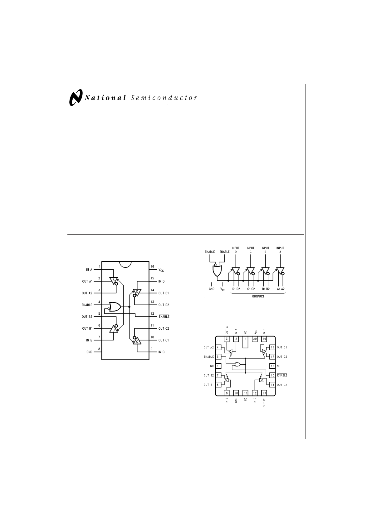
Connection and Logic Diagrams
TRI-STATE®is a registered trademark of National Semiconductor Corporation.
16-Lead Dual-In-Line Package
DS009614-1
Top View
For Complete Military Product Specifications,
refer to the appropriate SMD or MDS.
Order Number DS26F31ME/883, DS26F31MJ/883, or
DS26F31MW/883
See NS Package Numbers E20A, J16A, or W16A
DS009614-2
FIGURE 1. Logic Symbol
20-Lead Ceramic Leadless Chip Carrier (E)
DS009614-7
May 1999
DS26F31MQuad High Speed Differential Line Drivers
© 1999 National Semiconductor Corporation DS009614 www.national.com
Page 2
Absolute Maximum Ratings (Note 2)
If Military/Aerospace specified devices are required,
please contact the National Semiconductor Sales Office/
Distributors for availability and specifications.
Storage Temperature Range
Ceramic DIP −65˚C to +175˚C
Lead Temperature
Ceramic DIP (Soldering, 60 sec.) 300˚C
Maximum Power (Note 1) Dissipation at 25˚C
Cavity Package 1500 mW
Supply Voltage 7.0V
Input Voltage 7.0V
Output Voltage 5.5V
Operating Range
DS26F31M
Temperature −55˚C to +125˚C
Supply Voltage 4.5V to 5.5V
Note 1: Derate cavity package 10 mW/˚C above 25˚C.
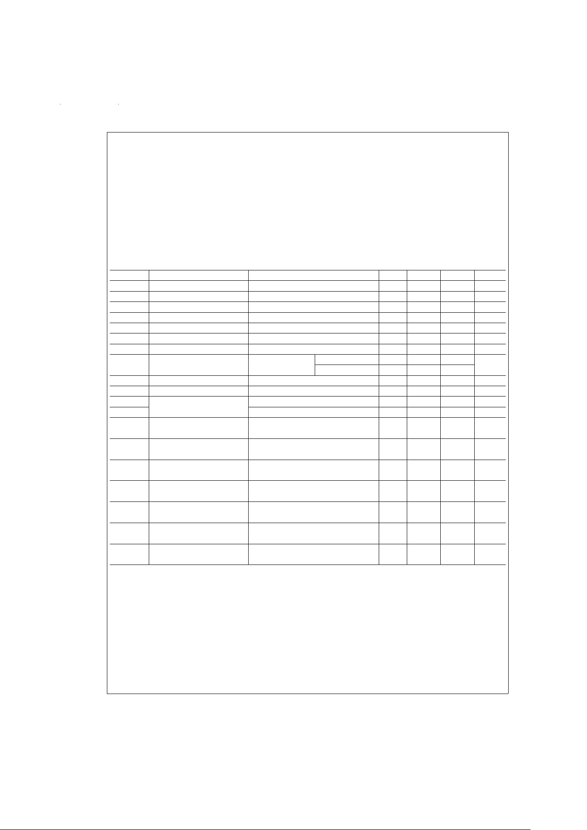
Electrical Characteristics (Notes 3, 4)
over operating range, unless otherwise specified
Symbol Parameter Conditions Min Typ Max Units
V
OH
Output Voltage HIGH V
CC
=
Min, I
OH
=
−20 mA 2.5 3.2 V
V
OL
Output Voltage LOW V
CC
=
Min, I
OL
=
20 mA 0.32 0.5 V
V
IH
Input Voltage HIGH V
CC
=
Min 2.0 V
V
IL
Input Voltage LOW V
CC
=
Max 0.8 V
I
IL
Input Current LOW V
CC
=
Max, V
I
=
0.4V −0.10 −0.20 mA
I
IH
Input Current HIGH V
CC
=
Max, V
I
=
2.7V 0.5 20 µA
I
IR
Input Reverse Current V
CC
=
Max, V
I
=
7.0V 0.001 0.1 mA
I
OZ
Off State (High Impedance) V
CC
=
Max V
O
=
2.5V 0.5 20 µA
Output Current V
O
=
0.5V 0.5 −20
V
IC
Input Clamp Voltage V
CC
=
Min, I
I
=
−18 mA −0.8 −1.5 V
I
OS
Output Short Circuit V
CC
=
Max (Note 5) −30 −60 −150 mA
I
CCX
Supply Current V
CC
=
Max, All Outputs Disabled 50 mA
I
CC
V
CC
=
Max, All Outputs Enabled 40 mA
t
PLH
Input to Output V
CC
=
5.0V, T
A
=
25˚C, 10 15 ns
Load=(Notes 6, 7)
t
PHL
Input to Output V
CC
=
5.0V, T
A
=
25˚C, 10 15 ns
Load=(Note 6)
SKEW Output to Output V
CC
=
5.0V, T
A
=
25˚C, 2.0 4.5 ns
Load=(Notes 6, 7)
t
LZ
Enable to Output V
CC
=
5.0V, T
A
=
25˚C, 23 32 ns
C
L
=
10 pF
t
HZ
Enable to Output V
CC
=
5.0V, T
A
=
25˚C, 15 25 ns
C
L
=
10 pF
t
ZL
Enable to Output V
CC
=
5.0V, T
A
=
25˚C, 20 30 ns
Load=(Note 6)
t
ZH
Enable to Output V
CC
=
5.0V, T
A
=
25˚C, 23 32 ns
Load=(Note 6)
Note 2: “Absolute Maximum Ratings” are those values beyond which the safety of the device cannot be guaranteed. They are not meant to imply that the devices
should be operated at these limits. The tables of “Electrical Characteristics” provide conditions for actual device operation.
Note 3: Unless otherwise specified min/max limits apply across the −55˚C to +125˚C temperature range for the DS26F31M and across the O˚C to +70˚C range for
the DS26F31C. All typicals are given for V
CC
=
5V and T
A
=
25˚C.
Note 4: All currents into the device pins are positive; all currents outof the device pins are negative.All voltagesare referenced to ground unless otherwise specified.
Note 5: Only one output at a time should be shorted.
Note 6: C
L
=
30 pF, V
I
=
1.3V to V
O
=
1.3V, V
PULSE
=
0V to +3V (See AC Load Test Circuit for TRI-STATE Outputs).
Note 7: Skew is defined as the difference in propagation delays between complementary outputs at the 50%point.
www.national.com 2
Page 3

Test Circuit and Timing Waveforms
Note 8: Diagram shown for Enable Low. Switches S1 and S2 open.
Note 9: S1 and S2 of Load Circuit are closed except where shown.
Note 10: Pulse Generator for all Pulses: Rate ≤ 1.0 MHz, Z
O
=
50Ω,t
r
≤6.0 ns, tf≤ 6.0 ns.
Note 11: C
L
includes probe and jig capacitance.
Typical Application
DS009614-3
FIGURE 2. AC Load Test Circuit for TRI-STATE Outputs
DS009614-4
FIGURE 3. Propagation Delay (Notes 2, 4)
DS009614-5
FIGURE 4. Enable and Disable Times (Notes 3, 4)
DS009614-6
FIGURE 5. Typical Application
www.national.com3
Page 4

Physical Dimensions inches (millimeters) unless otherwise noted
20-Lead Ceramic Leadless Chip Carrier (E)
DS26F31ME/883
NS Package Number E20A
16-Lead Ceramic Dual-In-Line Package (J)
DS26F31MJ/883
NS Package Number J16A
www.national.com 4
Page 5

Physical Dimensions inches (millimeters) unless otherwise noted (Continued)
LIFE SUPPORT POLICY
NATIONAL’S PRODUCTS ARE NOT AUTHORIZED FOR USE AS CRITICAL COMPONENTS IN LIFE SUPPORT
DEVICES OR SYSTEMS WITHOUT THE EXPRESS WRITTEN APPROVAL OF THE PRESIDENT AND GENERAL
COUNSEL OF NATIONAL SEMICONDUCTOR CORPORATION. As used herein:
1. Life support devices or systems are devices or
systems which, (a) are intended for surgical implant
into the body, or (b) support or sustain life, and
whose failure to perform when properly used in
accordance with instructions for use provided in the
labeling, can be reasonably expected to result in a
significant injury to the user.
2. A critical component is any component of a life
support device or system whose failure to perform
can be reasonably expected to cause the failure of
the life support device or system, or to affect its
safety or effectiveness.
National Semiconductor
Corporation
Americas
Tel: 1-800-272-9959
Fax: 1-800-737-7018
Email: support@nsc.com
National Semiconductor
Europe
Fax: +49 (0) 1 80-530 85 86
Email: europe.support@nsc.com
Deutsch Tel: +49 (0) 1 80-530 85 85
English Tel: +49 (0) 1 80-532 78 32
Français Tel: +49 (0) 1 80-532 93 58
Italiano Tel: +49 (0) 1 80-534 16 80
National Semiconductor
Asia Pacific Customer
Response Group
Tel: 65-2544466
Fax: 65-2504466
Email: sea.support@nsc.com
National Semiconductor
Japan Ltd.
Tel: 81-3-5639-7560
Fax: 81-3-5639-7507
www.national.com
16-Lead Ceramic Flatpak (W)
DS26F31MW/883
NS Package Number W16A
DS26F31MQuad High Speed Differential Line Drivers
National does not assume any responsibility for use of any circuitry described, no circuit patent licenses are implied and National reserves the right at any time without notice to change said circuitry and specifications.
 Loading...