

Page 1
DS26C32AT/DS26C32AM
Quad Differential Line Receiver
General Description
The DS26C32A is a quad differential line receiver designed
to meet the RS-422, RS-423, and Federal Standards 1020
and 1030for balanced and unbalanced digital data transmission, while retaining the low power characteristics of CMOS.
The DS26C32A has an input sensitivity of 200 mV over the
common mode input voltage range of
±
7V. The DS26C32A
features internal pull-up and pull-down resistors which prevent output oscillation on unused channels.
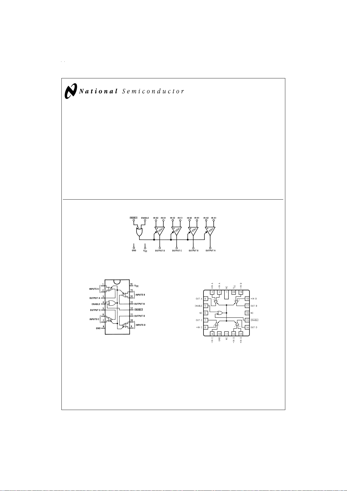
The DS26C32A provides an enable and disable function
common to all fourreceivers, and features TRI-STATE
®
outputs with 6 mAsource and sink capability. This product ispin
compatible with the DS26LS32A and the AM26LS32.
Features
n CMOS design for low power
n
±
0.2V sensitivity over input common mode voltage
range
n Typical propagation delays: 19 ns
n Typical input hysteresis: 60 mV
n Inputs won’t load line when V
CC
=
0V
n Meets the requirements of EIA standard RS-422
n TRI-STATE outputs for connection to system buses
n Available in Surface Mount
n Mil-Std-883C compliant
Logic Diagram
Connection Diagrams
TRI-STATE®is a registered trademark of National Semiconductor Corporation.
DS008764-1
Dual-In-Line Package
DS008764-2
Top View
Order Number DS26C32ATM or DS26C32ATN
See NS Package M16A or N16E
For Complete Military Product Specifications,
refer to the appropriate SMD or MDS.
Order Number DS26C32AME/883, DS26C32AMJ/883 or
DS26C32AMW/883
See NS Package E20A, J16A or W16A
20-Lead Ceramic Leadless Chip Carrier
DS008764-12
June 1998
DS26C32AT/DS26C32AM Quad Differential Line Receiver
© 1998 National Semiconductor Corporation DS008764 www.national.com
Page 2
Absolute Maximum Ratings (Notes 2, 1)
If Military/Aerospace specified devices are required,
please contact the National Semiconductor Sales Office/
Distributors for availability and specifications.
Supply Voltage (V
CC
)7V
Common Mode Range (V
CM
)
±
14V
Differential Input Voltage (V
DIFF
)
±
14V
Enable Input Voltage (V
IN
)7V
Storage Temperature Range (T
STG
) −65˚C to +150˚C
Lead Temperature (Soldering 4 sec.) 260˚C
Maximum Power Dissipation at 25˚C (Note 5)
Ceramic “J” Pkg. 2308 mW
Plastic “N” Pkg. 1645 mW
SOIC “M” Pkg. 1190 mW
Ceramic “E” Pkg. 2108 mW
Ceramic “W” Pkg. 1215 mW
Maximum Current Per Output
±
25 mA
This device does not meet 2000V ESD rating. (Note 4)
Operating Conditions
Min Max Units
Supply Voltage (V
CC
) 4.50 5.50 V
Operating Temperature Range (T
A
)
DS26C32AT −40 +85 ˚C
DS26C32AM −55 +125 ˚C
Enable Input Rise or Fall Times 500 ns
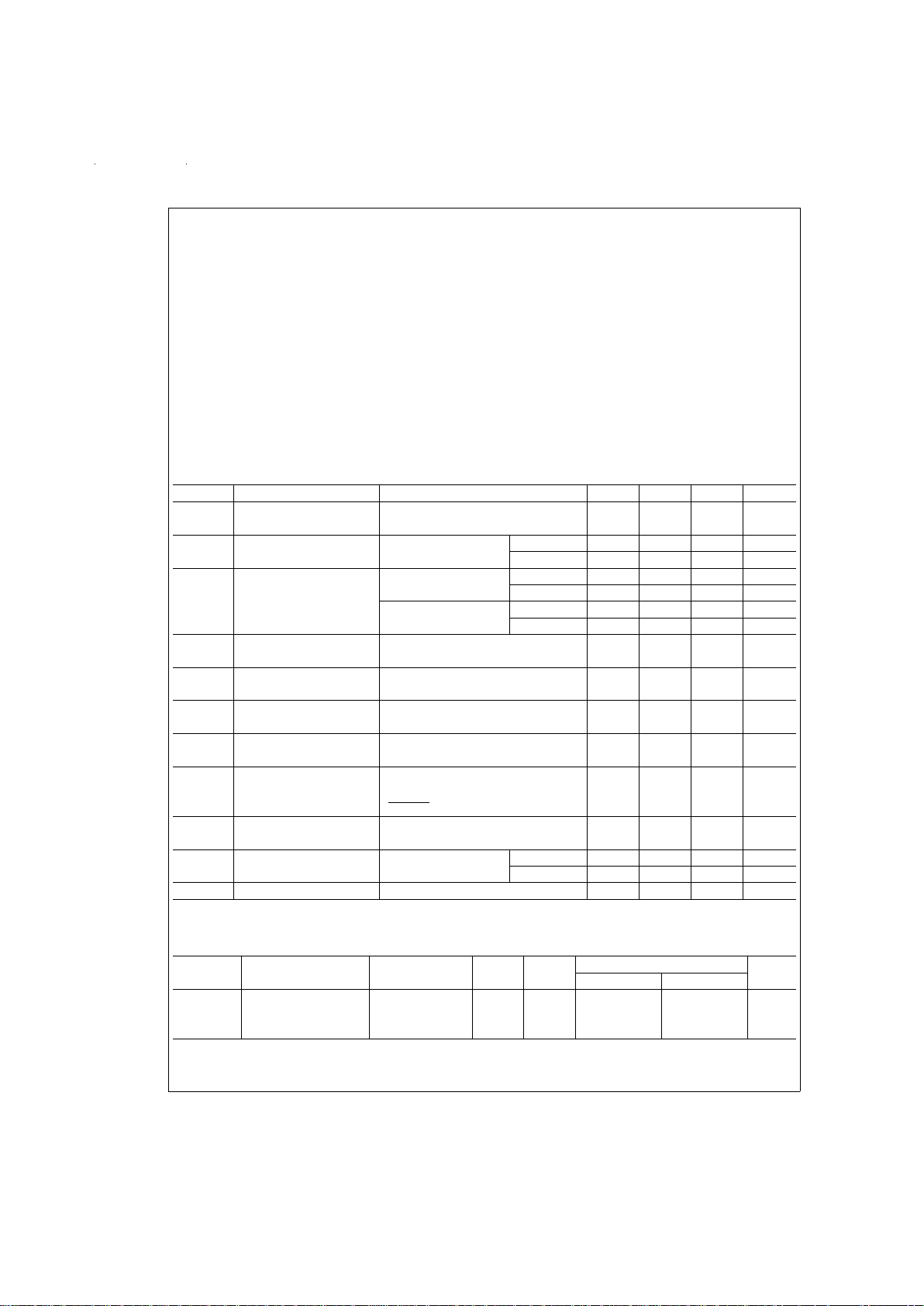
DC Electrical Characteristics
V
CC
=
5V
±
10%(unless otherwise specified) (Note 1)
Symbol Parameter Conditions Min Typ Max Units
V
TH
Minimum Differential V
OUT
=
V
OH
or V
OL
−200 35 +200 mV
Input Voltage −7V
<
V
CM
<
+7V
R
IN
Input Resistance V
IN
=
−7V, +7V DS26C32AT 5.0 6.8 10 kΩ
(Other Input=GND) DS26C32AM 4.5 6.8 11 kΩ
I
IN
Input Current V
IN
=
+10V, DS26C32AT +1.1 +1.5 mA
Other Input=GND DS26C32AM +1.1 +1.8 mA
V
IN
=
−10V, DS26C32AT −2.0 −2.5 mA
Other Input=GND DS26C32AM −2.0 −2.7 mA
V
OH
Minimum High Level V
CC
=
Min, V
DIFF
=
+1V 3.8 4.2 V
Output Voltage I
OUT
=
−6.0 mA
V
OL
Maximum Low Level V
CC
=
Max, V
DIFF
=
−1V 0.2 0.3 V
Output Voltage I
OUT
=
6.0 mA
V
IH
Minimum Enable High 2.0 V
Input Level Voltage
V
IL
Maximum Enable Low 0.8 V
Input Level Voltage
I
OZ
Maximum TRI-STATE
®
V
OUT
=
V
CC
or GND,
Output Leakage Current ENABLE=V
IL
,
±
0.5
±
5.0 µA
ENABLE=V
IH
I
I
Maximum Enable Input V
IN
=
V
CC
or GND
±
1.0 µA
Current
I
CC
Quiescent Power V
CC
=
Max, DS26C32AT 16 23 mA
Supply Current V
DIF
=
+1V DS26C32AM 16 25 mA
V
HYST
Input Hysteresis V
CM
=
0V 60 mV
AC Electrical Characteristics
V
CC
=
5V
±
10%(Note 3)
Symbol Parameter Conditions Min Typ Max Units
DS26C32AT DS26C32AM
t
PLH
, Propagation Delay C
L
=
50 pF
t
PHL
Input to Output V
DIFF
=
2.5V 10 19 30 35 ns
V
CM
=
0V
www.national.com 2
Page 3
AC Electrical Characteristics (Continued)
V
CC
=
5V
±
10%(Note 3)
Symbol Parameter Conditions Min Typ Max Units
DS26C32AT DS26C32AM
t
RISE
, Output Rise and C
L
=
50 pF
t
FALL
Fall Times V
DIFF
=
2.5V 4 9 9 ns
V
CM
=
0V
t
PLZ
, Propagation Delay C
L
=
50 pF
t
PHZ
ENABLE to Output R
L
=
1000Ω 13 22 29 ns
V
DIFF
=
2.5V
t
PZL
, Propagation Delay C
L
=
50 pF
t
PZH
ENABLE to Output R
L
=
1000Ω 13 23 29 ns
V
DIFF
=
2.5V
Note 1: Absolute Maximum Ratings are those values beyond which the safety of the device cannot be guaranteed. They are not meant to imply that the device
should be operated at these limits. The table of “Electrical Characteristics” provides conditions for actual device operation.
Note 2: Unless otherwise specified, all voltages are referenced to ground.
Note 3: Unless otherwise specified, Min/Max limits apply over recommended operating conditions. All typicals are given for V
CC
=
5V and T
A
=
25˚C.
Note 4: ESD Rating: HBM (1.5 kΩ, 100 pF)
Inputs ≥2000V
All other pins ≥1000V
EIAJ (0Ω, 200 pF) ≥350V
Note 5: Ratings apply toambient temperature at25˚C. Above this temperature derate NPackage 13.16 mW/˚C, J Package 15.38 mW/˚C, M Package 9.52 mW/˚C,
E Package 12.04 mW/˚C, and W package 6.94 mW/˚C.
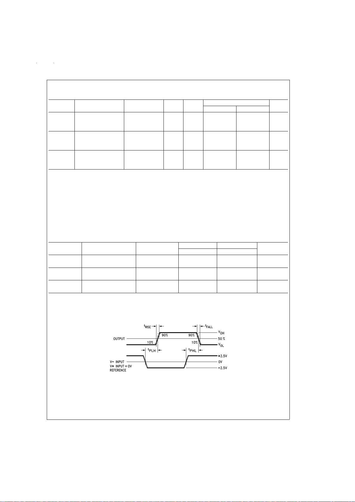
Comparison Table of Switching Characteristics into “LS-Type” Load
(
Figures 4, 5, 6
) (Note 6)
Symbol Parameter Conditions DS26C32A DS26LS32A Units
Typ Typ
t
PLH
Input to Output C
L
=
15 pF 17 23 ns
t
PHL
19 23 ns
t
LZ
ENABLE to Output C
L
=
5pF 13 15 ns
t
HZ
12 20 ns
t
ZL
ENABLE to Output C
L
=
15 pF 13 14 ns
t
ZH
13 15 ns
Note 6: This table is provided for comparison purposes only.The values in this table for the DS26C32A reflect the performance of the device, but are not tested or
guaranteed.
Test and Switching Waveforms
DS008764-3
FIGURE 1. Propagation Delay
www.national.com3
Page 4

Test and Switching Waveforms (Continued)
AC Test Circuit and Switching Time Waveforms
DS008764-4
CLincludes load and test jig capacitance.
S
1
=
V
CC
for t
PZL
, and t
PLZ
measurements.
S
1
=
Gnd for t
PZH
and t
PHZ
measurements.
FIGURE 2. Test Circuit for TRI-STATE Output Tests
DS008764-5
FIGURE 3. TRI-STATE®Output Enable and Disable Waveforms
DS008764-6
FIGURE 4. Load Test Circuit for TRI-STATE Outputs for “LS-Type” Load
DS008764-7
FIGURE 5. Propagation Delay for “LS-Type” Load (Notes 7, 9)
www.national.com 4
Page 5

AC Test Circuit and Switching Time Waveforms (Continued)
Note 7: Diagram shown for ENABLE low.
Note 8: S1 and S2 of load circuit are closed except where shown.
Note 9: Pulse generator for all pulses: Rate ≤ 1.0 MHz; Z
O
=
50Ω;t
r
≤15 ns; tf≤ 6.0 ns.
Truth Table
ENABLE ENABLE Input Output
LH X Z
All Other
Combinations of
Enable Inputs
V
ID
≥ VTH(Max) H
V
ID
≤ VTH(Min) L
Open H
Z=TRI-STATE
Typical Applications
Typical Performance Characteristics
DS008764-8
FIGURE 6. Enable and Disable Times for “LS-Type” Load (Notes 8, 9)
Two-Wire Balanced Systems, RS-422
DS008764-9
Differential Propagation Delay
vs Temperature
DS008764-13
Differential Propagation Delay
vs Power Supply Voltage
DS008764-14
Differential Skew vs
Temperature
DS008764-15
www.national.com5
Page 6

Typical Performance Characteristics (Continued)
Differential Skew vs Power
Supply Voltage
DS008764-16
Output High Voltage vs
Output High Current
DS008764-17
Output High Voltage vs
Output High Current
DS008764-18
Output Low Voltage vs
Output Low Current
DS008764-19
Output Low Voltage vs
Output Low Current
DS008764-20
Input Resistance vs
Input Voltage
DS008764-21
Input Current vs Power
Supply Voltage
DS008764-22
Hysteresis & Differential
Transition Voltage vs
Temperature
DS008764-23
Hysteresis & Differential
Transition Voltage vs
Power Supply Voltage
DS008764-24
www.national.com 6
Page 7

Typical Performance Characteristics (Continued)
Supply Current vs
Temperature
DS008764-25
Disabled Supply Current vs
Power Supply Voltage
DS008764-26
Supply Current vs
Data Rate
DS008764-27
www.national.com7
Page 8

Physical Dimensions inches (millimeters) unless otherwise noted
20-Lead Ceramic Leadless Chip Carrier (E)
Order Number DS26C32AME/883
NS Package Number E20A
16-Lead Ceramic Dual-In-Line Package (J)
Order Number DS26C32AMJ/883
NS Package Number J16A
www.national.com 8
Page 9

Physical Dimensions inches (millimeters) unless otherwise noted (Continued)
16-Lead Molded Small Outline Package (M)
Order Number DS26C32ATM
NS Package Number M16A
16-Lead Molded Dual-In-Line Package (N)
Order Number DS26C32ATN
NS Package Number N16E
www.national.com9
Page 10

Physical Dimensions inches (millimeters) unless otherwise noted (Continued)
LIFE SUPPORT POLICY
NATIONAL’S PRODUCTS ARE NOT AUTHORIZED FOR USE AS CRITICAL COMPONENTS IN LIFE SUPPORT DEVICES OR SYSTEMS WITHOUT THE EXPRESS WRITTEN APPROVAL OF THE PRESIDENT OF NATIONAL SEMICONDUCTOR CORPORATION. As used herein:
1. Life support devices or systems are devices or systems which, (a) are intended for surgical implant into
the body, or (b)support orsustain life,and whose failure to perform when properly used in accordance
with instructions for use provided in the labeling, can
be reasonably expected toresult ina significant injury
to the user.
2. A critical component in any component of a life support
device or system whose failure to perform can be reasonably expectedto cause thefailure of the life support
device or system, orto affectits safety or effectiveness.
National Semiconductor
Corporation
Americas
Tel: 1-800-272-9959
Fax: 1-800-737-7018
Email: support@nsc.com
www.national.com
National Semiconductor
Europe
Fax: +49 (0) 1 80-530 85 86
Email: europe.support@nsc.com
Deutsch Tel: +49 (0) 1 80-530 85 85
English Tel: +49 (0) 1 80-532 78 32
Français Tel: +49 (0) 1 80-532 93 58
Italiano Tel: +49 (0) 1 80-534 16 80
National Semiconductor
Asia Pacific Customer
Response Group
Tel: 65-2544466
Fax: 65-2504466
Email: sea.support@nsc.com
National Semiconductor
Japan Ltd.
Tel: 81-3-5639-7560
Fax: 81-3-5639-7507
16-Lead Ceramic FlatPak (W)
Order Number DS26C32AMW/883
NS Package Number W16A
DS26C32AT/DS26C32AM Quad Differential Line Receiver
National does not assume any responsibility for use of any circuitry described, no circuit patent licenses are implied and National reserves the right at any time without notice to change said circuitry and specifications.
 Loading...