

Page 1
DS26C31T/DS26C31M
CMOS Quad TRI-STATE
®
Differential Line Driver
General Description
The DS26C31 is a quad differential line driver designed for
digital data transmission over balanced lines. The
DS26C31T meets all the requirements of EIA standard
RS-422 while retaining the low power characteristics of
CMOS. The DS26C31M is compatible with EIA standard
RS-422; however, one exception in test methodology is
taken (Note 8). This enables the construction of serial and
terminal interfaces while maintaining minimal power consumption.
The DS26C31accepts TTL or CMOS input levels and translates these to RS-422 output levels. This part uses special
output circuitry that enables the drivers to power down without loading down the bus. This device has enable and disable circuitry common to all four drivers. The DS26C31 is pin
compatible to the AM26LS31 and the DS26LS31.
All inputs are protected against damage due to electrostatic
discharge by diodes to V
CC
and ground.
Features
n TTL input compatible
n Typical propagation delays: 6 ns
n Typical output skew: 0.5 ns
n Outputs will not load line when V
CC
=
0V
n DS26C31T meets the requirements of EIA standard
RS-422
n Operation from single 5V supply
n TRI-STATE outputs for connection to system buses
n Low quiescent current
n Available in surface mount
n Mil-Std-883C compliant
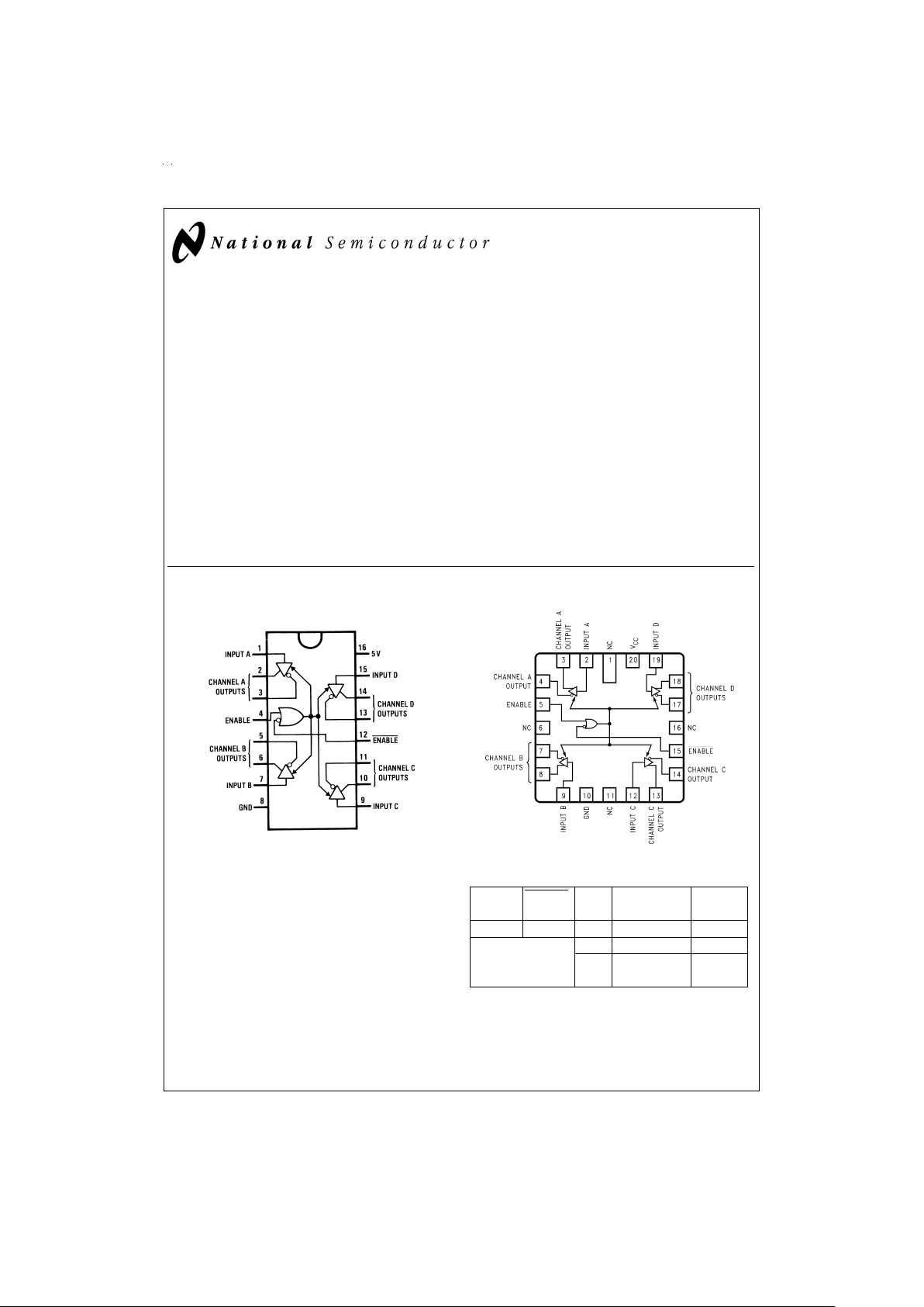
Connection Diagrams
Truth Table
ENABLE ENABLE Input Non-Inverting Inverting
Output Output
LHX Z Z
All other L L H
combinations of H H L
enable inputs
L=Low logic state
X=Irrelevant
H=High logic state
Z=TRI-STATE (high impedance)
TRI-STATE®is a registered trademark of National Semiconductor Corporation.
FACT
™
is a trademark of National Semiconductor Corporation.
Dual-In-Line Package
DS008574-1
Top View
Order Number DS26C31TM or DS26C31TN
See NS Package Number M16A or N16E
For Complete Military Product Specifications,
refer to the appropriate SMD or MDS.
Order Number DS26C31ME/883, DS26C31MJ/883
or DS26C31MW/883
See NS Package Number E20A, J16A or W16A
20-Lead Ceramic Leadless Chip Carrier (E)
DS008574-12
June 1998
DS26C31T/DS26C31M CMOS Quad TRI-STATE Differential Line Driver
© 1998 National Semiconductor Corporation DS008574 www.national.com
Page 2
Absolute Maximum Ratings (Notes 1, 2)
If Military/Aerospace specified devices are required,
please contact the National Semiconductor Sales Office/
Distributors for availability and specifications.
Supply Voltage (V
CC
) −0.5V to 7.0V
DC Input Voltage (V
IN
) −1.5V to VCC+1.5V
DC Output Voltage (V
OUT
) −0.5V to 7V
Clamp Diode Current (I
IK,IOK
)
±
20 mA
DC Output Current, per pin (I
OUT
)
±
150 mA
DC V
CC
or GND Current,
per pin (I
CC
)
±
150 mA
Storage Temperature Range (T
STG
) −65˚C to +150˚C
Max. Power Dissipation (P
D
)@25˚C (Note 3)
Ceramic “J” Pkg. 2419 mW
Plastic “N” Pkg. 1736 mW
SOIC “M” Pkg. 1226 mW
Ceramic “W” Pkg. 1182 mW
Ceramic “E” Pkg. 2134 mW
Lead Temperature (T
L
)
(Soldering, 4 sec.) 260˚C
This device does not meet 2000V ESD Rating. (Note 13)
Operating Conditions
Min Max Units
Supply Voltage (V
CC
) 4.50 5.50 V
DC Input or Output Voltage
(V
IN,VOUT
)0V
CC
V
Operating Temperature Range (T
A
)
DS26C31T −40 +85 ˚C
DS26C31M −55 +125 ˚C
Input Rise or Fall Times (t
r,tf
) 500 ns
DC Electrical Characteristics
V
CC
=
5V
±
10%(unless otherwise specified) (Note 4)
Symbol Parameter Conditions Min Typ Max Units
V
IH
High Level Input Voltage 2.0 V
V
IL
Low Level Input Voltage 0.8 V
V
OH
High Level Output Voltage V
IN
=
V
IH
or VIL, 2.5 3.4 V
I
OUT
=
−20 mA
V
OL
Low Level Output V
IN
=
V
IH
or VIL, 0.3 0.5 V
Voltage I
OUT
=
20 mA
V
T
Differential Output R
L
=
100Ω 2.0 3.1 V
Voltage (Note 5)
|V
T
|−|VT| Difference In R
L
=
100Ω 0.4 V
Differential Output (Note 5)
V
OS
Common Mode R
L
=
100Ω 1.8 3.0 V
Output Voltage (Note 5)
|V
OS−VOS
| Difference In R
L
=
100Ω 0.4 V
Common Mode Output (Note 5)
I
IN
Input Current V
IN
=
V
CC
, GND, VIH,orV
IL
±
1.0 µA
I
CC
Quiescent Supply DS26C31T V
IN
=
V
CC
or GND 200 500 µA
Current (Note 6) I
OUT
=
0µA V
IN
=
2.4V or 0.5V 0.8 2.0 mA
(Note 6)
DS26C31M V
IN
=
V
CC
or GND 200 500 µA
I
OUT
=
0µA V
IN
=
2.4V or 0.5V 0.8 2.1 mA
(Note 6)
I
OZ
TRI-STATE Output V
OUT
=
V
CC
or GND
Leakage Current ENABLE=V
IL
±
0.5
±
5.0 µA
ENABLE=V
IH
I
SC
Output Short V
IN
=
V
CC
or GND −30 −150 mA
Circuit Current (Notes 5, 7)
www.national.com 2
Page 3
DC Electrical Characteristics (Continued)
V
CC
=
5V
±
10%(unless otherwise specified) (Note 4)
Symbol Parameter Conditions Min Typ Max Units
I
OFF
Output Leakage Current DS26C31T V
OUT
=
6V 100 µA
Power Off (Note 5) V
CC
=
0V V
OUT
=
−0.25V −100 µA
DS26C31M V
OUT
=
6V 100 µA
V
CC
=
0V V
OUT
=
0V −100 µA
(Note 8)
Note 1: Absolute Maximum Ratings are those values beyond which the safety of the device cannot be guaranteed. They are not meant to imply that the device
should be operated at these limits. The table of “Electrical Characteristics” provide conditions for actual device operation.
Note 2: Unless otherwise specified, all voltages are referenced to ground. All currents into device pins are positive, all currents out of device pins are negative.
Note 3: Ratings apply to ambient temperature at 25˚C.Abovethistemperaturederate N package at 13.89 mW/˚C, J package 16.13mW/˚C,Mpackage9.80 mW/˚C,
E package 12.20 mW/˚C, and W package 6.75 mW/˚C.
Note 4: Unless otherwise specified, min/max limits apply across the recommended operating temperature range. All typicals are given for V
CC
=
5V and T
A
=
25˚C.
Note 5: See EIA Specification RS-422 for exact test conditions.
Note 6: Measured per input. All other inputs at V
CC
or GND.
Note 7: This is the current sourced when a high output is shorted to ground. Only one output at a time should be shorted.
Note 8: The DS26C31M (−55˚C to +125˚C) is tested with V
OUT
between +6V and 0V while RS-422A condition is +6V and −0.25V.
Switching Characteristics
V
CC
=
5V
±
10%,tr≤6 ns, tf≤ 6ns(
Figures 1, 2, 3, 4
) (Note 4)
Symbol Parameter Conditions Min Typ Max Units
DS26C31T CS26C31M
t
PLH,tPHL
Propagation Delays S1 Open 2 6 11 14 ns
Input to Output
Skew (Note 9) S1 Open 0.5 2.0 3.0 ns
t
TLH,tTHL
Differential Output Rise S1 Open 6 10 14 ns
And Fall Times
t
PZH
Output Enable Time S1 Closed 11 19 22 ns
t
PZL
Output Enable Time S1 Closed 13 21 28 ns
t
PHZ
Output Disable Time S1 Closed 5 9 12 ns
(Note 10)
t
PLZ
Output Disable Time S1 Closed 7 11 14 ns
(Note 10)
C
PD
Power Dissipation 50 pF
Capacitance (Note 11)
C
IN
Input Capacitance 6 pF
Note 9: Skew is defined as the difference in propagation delays between complementary outputs at the 50%point.
Note 10: Output disable time is the delay from ENABLE or ENABLE being switched to the output transistors turning off. The actual disable times are less than in-
dicated due to the delay added by the RC time constant of the load.
Note 11: C
PD
determines the no load dynamic power consumption, P
D
=
C
PDVCC
2f+ICCVCC, and the no load dynamic current consumption, I
S
=
C
PDVCC
f+
I
CC
.
Comparison Table of Switching Characteristics into “LS-Type” Load
V
CC
=
5V, T
A
=
25˚C, t
r
≤ 6 ns, tf≤ 6ns(
Figures 2, 4, 5, 6
) (Note 12)
Symbol Parameter Conditions DS26C31T DS26LS31C Units
Typ Max Typ Max
t
PLH,tPHL
Propagation Delays C
L
=
30 pF
Input to Output S1 Closed 6 8 10 15 ns
S2 Closed
Skew (Note 9) C
L
=
30 pF
S1 Closed 0.5 1.0 2.0 6.0 ns
S2 Closed
www.national.com3
Page 4
Comparison Table of Switching Characteristics into “LS-Type” Load
(Continued)
V
CC
=
5V, T
A
=
25˚C, t
r
≤ 6 ns, tf≤ 6ns(
Figures 2, 4, 5, 6
) (Note 12)
Symbol Parameter Conditions DS26C31T DS26LS31C Units
Typ Max Typ Max
t
THL,tTLH
Differential Output Rise C
L
=
30 pF
and Fall Times S1 Closed 4 6 ns
S2 Closed
t
PLZ
Output Disable Time C
L
=
10 pF
(Note 10) S1 Closed 6 9 15 35 ns
S2 Open
t
PHZ
Output Disable Time C
L
=
10 pF
(Note 10) S1 Open 4 7 15 25 ns
S2 Closed
t
PZL
Output Enable Time C
L
=
30 pF
S1 Closed 14 20 20 30 ns
S2 Open
t
PZH
Output Enable Time C
L
=
30 pF
S1 Open 11 17 20 30 ns
S2 Closed
Note 12: This table is provided for comparison purposes only. The values in this table for the DS26C31 reflect the performance of the device but are not tested or
guaranteed.
Note 13: ESD Rating:
HBM (1.5 kΩ, 100 pF)
Inputs ≥ 1500V
Outputs ≥ 1000V
EIAJ (0Ω, 200 pF) ≥ 350V
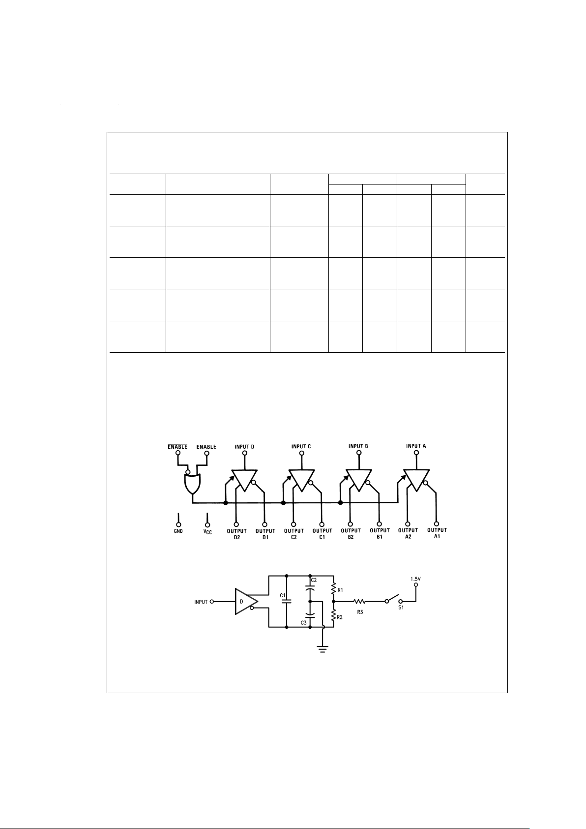
Logic Diagram
AC Test Circuit and Switching Time Waveforms
DS008574-2
DS008574-3
Note: C1=C2=C3=40 pF (Including Probe and Jig Capacitance), R1=R2=50Ω,R3=500Ω.
FIGURE 1. AC Test Circuit
www.national.com 4
Page 5

AC Test Circuit and Switching Time Waveforms (Continued)
DS008574-4
FIGURE 2. Propagation Delays
DS008574-5
FIGURE 3. Enable and Disable Times
DS008574-7
Input pulse; f=1 MHz, 50%;tr≤6 ns, tf≤ 6ns
FIGURE 4. Differential Rise and Fall Times
www.national.com5
Page 6

AC Test Circuit and Switching Time Waveforms (Continued)
Typical Applications
DS008574-6
FIGURE 5. Load AC Test Circuit for “LS-Type” Load
DS008574-8
FIGURE 6. Enable and Disable Times for “LS-Type” Load
Two-Wire Balanced System, RS-422
DS008574-9
*RTis optional although highly recommended to reduce reflection.
www.national.com 6
Page 7

Typical Performance Characteristics
Differential Propagation Delay
vs Temperature
DS008574-14
Differential Propagation Delay
vs Power Supply Voltage
DS008574-15
Differential Skew vs
Temperature
DS008574-16
Differential Skew vs Power
Supply Voltage
DS008574-17
Differential Transition Time
vs Temperature
DS008574-18
Differential Transition Time
vs Power Supply Voltage
DS008574-19
Complementary Skew vs
Temperature
DS008574-20
Complementary Skew vs
Power Supply Voltage
DS008574-21
Differential Output Voltage
vs Output Current
DS008574-22
www.national.com7
Page 8

Typical Performance Characteristics (Continued)
Differential Output Voltage
vs Output Current
DS008574-23
Output High Voltage vs
Output High Current
DS008574-24
Output High Voltage vs
Output High Current
DS008574-25
Output Low Voltage vs
Output Low Current
DS008574-26
Output Low Voltage vs
Output Low Current
DS008574-27
Supply Current
vs Temperature
DS008574-28
Supply Current vs
Power Supply Voltage
DS008574-29
No Load Supply Current
vs Data Rate
DS008574-30
Loaded Supply Current
vs Data Rate
DS008574-31
www.national.com 8
Page 9

Typical Performance Characteristics (Continued)
Output Short Circuit Current
vs Temperature
DS008574-32
Output Short Circuit Current
vs Power Supply Voltage
DS008574-33
www.national.com9
Page 10

Physical Dimensions inches (millimeters) unless otherwise noted
20-Lead Ceramic Leadless Chip Carrier (E)
Order Number DS26C31ME/883
NS Package Number E20A
16-Lead Ceramic Dual-In-Line Package (J)
Order Number DS26C31MJ/883
NS Package Number J16A
www.national.com 10
Page 11

Physical Dimensions inches (millimeters) unless otherwise noted (Continued)
Molded Package Small Outline (M)
Order Number DS26C31TM
NS Package Number M16A
16-Lead Molded Dual-In-Line Package (N)
Order Number DS26C31TN
NS Package Number N16E
www.national.com11
Page 12

Physical Dimensions inches (millimeters) unless otherwise noted (Continued)
LIFE SUPPORT POLICY
NATIONAL’S PRODUCTS ARE NOT AUTHORIZED FOR USE AS CRITICAL COMPONENTS IN LIFE SUPPORT DEVICES OR SYSTEMS WITHOUT THE EXPRESS WRITTEN APPROVAL OF THE PRESIDENT OF NATIONAL SEMICONDUCTOR CORPORATION. As used herein:
1. Life support devices or systems are devices or systems which, (a) are intended for surgical implant into
the body, or (b) support or sustain life, and whosefailure to perform when properly used in accordance
with instructions for use provided in the labeling, can
be reasonably expected to result in a significant injury
to the user.
2. A critical component in any component of a life support
device or system whose failure to perform can be reasonably expected to cause the failure of the life support
device or system, or to affect its safety or effectiveness.
National Semiconductor
Corporation
Americas
Tel: 1-800-272-9959
Fax: 1-800-737-7018
Email: support@nsc.com
www.national.com
National Semiconductor
Europe
Fax: +49 (0) 1 80-530 85 86
Email: europe.support@nsc.com
Deutsch Tel: +49 (0) 1 80-530 85 85
English Tel: +49 (0) 1 80-532 78 32
Français Tel: +49 (0) 1 80-532 93 58
Italiano Tel: +49 (0) 1 80-534 16 80
National Semiconductor
Asia Pacific Customer
Response Group
Tel: 65-2544466
Fax: 65-2504466
Email: sea.support@nsc.com
National Semiconductor
Japan Ltd.
Tel: 81-3-5620-6175
Fax: 81-3-5620-6179
16-Lead Ceramic Flatpak Package (W)
Order Number DS26C31MW/883
NS Package Number W16A
DS26C31T/DS26C31M CMOS Quad TRI-STATE Differential Line Driver
National does not assume any responsibility for use of any circuitry described, no circuit patent licenses are implied and National reserves the right at any time without notice to change said circuitry and specifications.
 Loading...