

Page 1
1 of 286
REV: 022007
Note: Some revisions of this device may incorporate deviations from published specifications known as errata. Multiple revisions of any device
may be simultaneously available through various sales channels. For information about device errata, click here: www.maxim-ic.com/errata
.
DS26518
8-Port T1/E1/J1 Transceive
r
GENERAL DESCRIPTION
The DS26518 is a single-chip 8-port framer and line
interface unit (LIU) combination for T1, E1, and J1
applications. Each port is independently configurable,
supporting both long-haul and short-haul lines. The
8-port SCT is software compatible with the DS26519
and nearly software compatible with the DS26528
and its derivatives.
APPLICATIONS
Routers
Channel Service Units (CSUs)
Data Service Units (DSUs)
Muxes
Switches
Channel Banks
T1/E1 Test Equipment
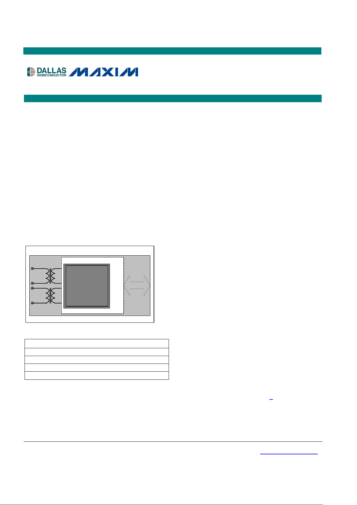
FUNCTIONAL DIAGRAM
DS26518
T1/J1/E1
Transceiver
T1/E1/J1
NETWORK
BACKPLANE
TDM
x8
ORDERING INFORMATION
PART TEMP RANGE PIN-PACKAGE
DS26518G
0°C to +70°C
256 TE-CSBGA
DS26518G+
0°C to +70°C
256 TE-CSBGA
DS26518GN
-40°C to +85°C
256 TE-CSBGA
DS26518GN+
-40°C to +85°C
256 TE-CSBGA
+ Denotes lead-free/RoHS compliant device.
FEATURES
Eight Complete T1, E1, or J1 Long-Haul/
Short-Haul Transceivers (LIU Plus Framer)
Independent T1, E1, or J1 Selections for Each
Transceiver
Fully Internal Impedance Match, No External
Resistor
Software-Selectable Transmit- and Receive-
Side Termination for 100Ω T1 Twisted Pair,
110Ω J1 Twisted Pair, 120Ω E1 Twisted Pair,
and 75Ω E1 Coaxial Applications
Hitless Protection Switching
Crystal-Less Jitter Attenuators Can Be
Selected for Transmit or Receive Path; Jitter
Attenuator Meets ETS CTR 12/13, ITU-T
G.736, G.742, G.823, and AT&T Pub 62411
External Master Clock Can Be Multiple of
2.048MHz or 1.544MHz for T1/J1 or E1
Operation; This Clock is Internally Adapted
for T1 or E1 Usage in the Host Mode
Receive-Signal Level Indication from -2.5dB
to -36dB in T1 Mode and -2.5dB to -44dB in E1
Mode in Approximate 2.5dB Increments
Transmit Open- and Short-Circuit Detection
LIU LOS in Accordance with G.775, ETS 300
233, and T1.231
Transmit Synchronizer
Flexible Signaling Extraction and Insertion
Using Either the System Interface or
Microprocessor Port
Alarm Detection and Insertion
T1 Framing Formats of D4, SLC-96, and ESF
J1 Support
E1 G.704 and CRC-4 Multiframe
T1-to-E1 Conversion
Features Continued in Section 2.
www.maxim-ic.com
Page 2

DS26518 8-Port T1/E1/J1 Transceiver
2 of 286
TABLE OF CONTENTS
1. DETAILED DESCRIPTION.................................................................................................9
2. FEATURE HIGHLIGHTS..................................................................................................10
2.1 GENERAL......................................................................................................................................10
2.2 LINE INTERFACE............................................................................................................................10
2.3 CLOCK SYNTHESIZERS ..................................................................................................................10
2.4 JITTER ATTENUATOR.....................................................................................................................10
2.5 FRAMER/FORMATTER....................................................................................................................11
2.6 SYSTEM INTERFACE ......................................................................................................................11
2.7 HDCL CONTROLLERS ...................................................................................................................12
2.8 TEST AND DIAGNOSTICS................................................................................................................12
2.9 MICROCONTROLLER PARALLEL PORT.............................................................................................12
2.10 SLAVE SERIAL PERIPHERAL INTERFACE (SPI) FEATURES ............................................................12
3. APPLICATIONS ...............................................................................................................13
4. SPECIFICATIONS COMPLIANCE...................................................................................14
5. ACRONYMS AND GLOSSARY .......................................................................................16
6. MAJOR OPERATING MODES .........................................................................................17
7. BLOCK DIAGRAMS......................................................................................................... 18
8. PIN DESCRIPTIONS ........................................................................................................20
8.1 PIN FUNCTIONAL DESCRIPTION......................................................................................................20
9. FUNCTIONAL DESCRIPTION .........................................................................................28
9.1 PROCESSOR INTERFACE................................................................................................................28
9.1.1 SPI Serial Port Mode............................................................................................................................ 28
9.1.2 SPI Functional Timing Diagrams ......................................................................................................... 28
9.2 CLOCK STRUCTURE.......................................................................................................................31
9.2.1 Backplane Clock Generation ............................................................................................................... 31
9.2.2 CLKO Output Clock Generation........................................................................................................... 32
9.3 RESETS AND POWER-DOWN MODES..............................................................................................33
9.4 INITIALIZATION AND CONFIGURATION..............................................................................................34
9.4.1 Example Device Initialization and Sequence.......................................................................................34
9.5 GLOBAL RESOURCES ....................................................................................................................34
9.6 PER-PORT RESOURCES ................................................................................................................34
9.7 DEVICE INTERRUPTS .....................................................................................................................34
9.8 SYSTEM BACKPLANE INTERFACE ...................................................................................................36
9.8.1 Elastic Stores....................................................................................................................................... 36
9.8.2 IBO Multiplexing................................................................................................................................... 39
9.8.3 H.100 (CT Bus) Compatibility .............................................................................................................. 45
9.8.4 Transmit and Receive Channel Blocking Registers............................................................................. 47
9.8.5 Transmit Fractional Support (Gapped Clock Mode)............................................................................ 47
9.8.6 Receive Fractional Support (Gapped Clock Mode)............................................................................. 47
9.9 FRAMERS......................................................................................................................................48
9.9.1 T1 Framing...........................................................................................................................................48
9.9.2 E1 Framing........................................................................................................................................... 51
9.9.3 T1 Transmit Synchronizer.................................................................................................................... 53
9.9.4 Signaling .............................................................................................................................................. 54
9.9.5 T1 Data Link.........................................................................................................................................59
9.9.6 E1 Data Link......................................................................................................................................... 61
9.9.7 Maintenance and Alarms..................................................................................................................... 62
Page 3

DS26518 8-Port T1/E1/J1 Transceiver
3 of 286
9.9.8 Alarms.................................................................................................................................................. 65
9.9.9 Error Count Registers .......................................................................................................................... 67
9.9.10 DS0 Monitoring Function...................................................................................................................... 69
9.9.11 Transmit Per-Channel Idle Code Generation ...................................................................................... 70
9.9.12 Receive Per-Channel Idle Code Insertion............................................................................................ 70
9.9.13 Per-Channel Loopback ........................................................................................................................ 70
9.9.14 E1 G.706 Intermediate CRC-4 Updating (E1 Mode Only)................................................................... 70
9.9.15 T1 Programmable In-Band Loop Code Generator............................................................................... 71
9.9.16 T1 Programmable In-Band Loop Code Detection................................................................................ 72
9.9.17 Framer Payload Loopbacks................................................................................................................. 73
9.10 HDLC CONTROLLERS................................................................................................................74
9.10.1 Receive HDLC Controller.....................................................................................................................74
9.10.2 Transmit HDLC Controller.................................................................................................................... 77
9.11 POWER-SUPPLY DECOUPLING....................................................................................................79
9.12 LINE INTERFACE UNITS (LIUS)....................................................................................................80
9.12.1 LIU Operation.......................................................................................................................................82
9.12.2 Transmitter........................................................................................................................................... 83
9.12.3 Receiver............................................................................................................................................... 86
9.12.4 Hitless Protection Switching (HPS)......................................................................................................90
9.12.5 Jitter Attenuator....................................................................................................................................91
9.12.6 LIU Loopbacks..................................................................................................................................... 92
9.13 BIT ERROR-RATE TEST FUNCTION (BERT).................................................................................95
9.13.1 BERT Repetitive Pattern Set ............................................................................................................... 96
9.13.2 BERT Error Counter............................................................................................................................. 96
10. DEVICE REGISTERS.......................................................................................................97
10.1 REGISTER LISTINGS ...................................................................................................................97
10.1.1 Global Register List.............................................................................................................................. 98
10.1.2 Framer Register List............................................................................................................................. 99
10.1.3 LIU and BERT Register List...............................................................................................................106
10.2 REGISTER BIT MAPS ................................................................................................................107
10.2.1 Global Register Bit Map..................................................................................................................... 107
10.2.2 Framer Register Bit Map.................................................................................................................... 108
10.2.3 LIU Register Bit Map.......................................................................................................................... 117
10.2.4 BERT Register Bit Map......................................................................................................................118
10.3 GLOBAL REGISTER DEFINITIONS...............................................................................................119
10.4 FRAMER REGISTER DESCRIPTIONS...........................................................................................133
10.4.1 Receive Register Descriptions........................................................................................................... 133
10.4.2 Transmit Register Descriptions..........................................................................................................191
10.5 LIU REGISTER DEFINITIONS .....................................................................................................227
10.6 BERT REGISTER DEFINITIONS .................................................................................................237
11. FUNCTIONAL TIMING ...................................................................................................245
11.1 T1 RECEIVER FUNCTIONAL TIMING DIAGRAMS ..........................................................................245
11.2 T1 TRANSMITTER FUNCTIONAL TIMING DIAGRAMS ....................................................................250
11.3 E1 RECEIVER FUNCTIONAL TIMING DIAGRAMS..........................................................................255
11.4 E1 TRANSMITTER FUNCTIONAL TIMING DIAGRAMS ....................................................................259
12. OPERATING PARAMETERS.........................................................................................264
12.1 THERMAL CHARACTERISTICS....................................................................................................265
12.2 LINE INTERFACE CHARACTERISTICS..........................................................................................265
13. AC TIMING CHARACTERISTICS..................................................................................266
13.1 MICROPROCESSOR BUS AC CHARACTERISTICS........................................................................266
13.1.1 SPI Bus Mode.................................................................................................................................... 266
13.2 JTAG INTERFACE TIMING.........................................................................................................277
14. JTAG BOUNDARY SCAN AND TEST ACCESS PORT................................................278
Page 4

DS26518 8-Port T1/E1/J1 Transceiver
4 of 286
14.1 TAP CONTROLLER STATE MACHINE.........................................................................................279
14.1.1 Test-Logic-Reset................................................................................................................................ 279
14.1.2 Run-Test-Idle ..................................................................................................................................... 279
14.1.3 Select-DR-Scan ................................................................................................................................. 279
14.1.4 Capture-DR........................................................................................................................................ 279
14.1.5 Shift-DR.............................................................................................................................................. 279
14.1.6 Exit1-DR.............................................................................................................................................279
14.1.7 Pause-DR........................................................................................................................................... 279
14.1.8 Exit2-DR.............................................................................................................................................279
14.1.9 Update-DR......................................................................................................................................... 279
14.1.10 Select-IR-Scan ............................................................................................................................... 279
14.1.11 Capture-IR...................................................................................................................................... 280
14.1.12 Shift-IR............................................................................................................................................ 280
14.1.13 Exit1-IR...........................................................................................................................................280
14.1.14 Pause-IR......................................................................................................................................... 280
14.1.15 Exit2-IR...........................................................................................................................................280
14.1.16 Update-IR....................................................................................................................................... 280
14.2 INSTRUCTION REGISTER...........................................................................................................282
14.2.1 SAMPLE:PRELOAD .......................................................................................................................... 282
14.2.2 BYPASS.............................................................................................................................................282
14.2.3 EXTEST ............................................................................................................................................. 282
14.2.4 CLAMP...............................................................................................................................................282
14.2.5 HIGHZ................................................................................................................................................ 282
14.2.6 IDCODE............................................................................................................................................. 282
14.3 JTAG ID CODES......................................................................................................................283
14.4 TEST REGISTERS.....................................................................................................................283
14.4.1 Boundary Scan Register.................................................................................................................... 283
14.4.2 Bypass Register................................................................................................................................. 283
14.4.3 Identification Register......................................................................................................................... 283
15. PIN CONFIGURATION...................................................................................................284
15.1 PIN CONFIGURATION—256-BALL TE-CSBGA ..........................................................................284
16. PACKAGE INFORMATION............................................................................................285
16.1 256-BALL TE-CSBGA (56-G6028-001)...................................................................................285
17. DOCUMENT REVISION HISTORY ................................................................................286
Page 5

DS26518 8-Port T1/E1/J1 Transceiver
5 of 286
LIST OF FIGURES
Figure 7-1. Block Diagram......................................................................................................................................... 18
Figure 7-2. Detailed Block Diagram........................................................................................................................... 19
Figure 9-1. SPI Serial Port Access for Read Mode, SPI_CPOL = 0, SPI_CPHA = 0............................................... 29
Figure 9-2. SPI Serial Port Access for Read Mode, SPI_CPOL = 1, SPI_CPHA = 0............................................... 29
Figure 9-3. SPI Serial Port Access for Read Mode, SPI_CPOL = 0, SPI_CPHA = 1............................................... 29
Figure 9-4. SPI Serial Port Access for Read Mode, SPI_CPOL = 1, SPI_CPHA = 1............................................... 29
Figure 9-5. SPI Serial Port Access for Write Mode, SPI_CPOL = 0, SPI_CPHA = 0 ............................................... 30
Figure 9-6. SPI Serial Port Access for Write Mode, SPI_CPOL = 1, SPI_CPHA = 0 ............................................... 30
Figure 9-7. SPI Serial Port Access for Write Mode, SPI_CPOL = 0, SPI_CPHA = 1 ............................................... 30
Figure 9-8. SPI Serial Port Access for Write Mode, SPI_CPOL = 1, SPI_CPHA = 1 ............................................... 30
Figure 9-9. Backplane Clock Generation................................................................................................................... 31
Figure 9-10. Device Interrupt Information Flow Diagram........................................................................................... 35
Figure 9-11. IBO Multiplexer Equivalent Circuit—4.096MHz .................................................................................... 40
Figure 9-12. IBO Multiplexer Equivalent Circuit—8.192MHz .................................................................................... 41
Figure 9-13. IBO Multiplexer Equivalent Circuit—16.384MHz .................................................................................. 42
Figure 9-14. RSYNCn Input in H.100 (CT Bus) Mode...............................................................................................46
Figure 9-15. TSSYNCIOn (Input Mode) Input in H.100 (CT Bus) Mode ................................................................... 46
Figure 9-16. CRC-4 Recalculate Method .................................................................................................................. 70
Figure 9-17. HDLC Message Receive Example........................................................................................................76
Figure 9-18. HDLC Message Transmit Example.......................................................................................................78
Figure 9-19. Network Connection—Longitudinal Protection ..................................................................................... 81
Figure 9-20. T1/J1 Transmit Pulse Templates .......................................................................................................... 84
Figure 9-21. E1 Transmit Pulse Templates............................................................................................................... 85
Figure 9-22. Receive LIU Termination Options......................................................................................................... 87
Figure 9-23. Typical Monitor Application ................................................................................................................... 88
Figure 9-24. HPS Block Diagram............................................................................................................................... 90
Figure 9-25. Jitter Attenuation ................................................................................................................................... 91
Figure 9-26. Loopback Diagram................................................................................................................................ 92
Figure 9-27. Analog Loopback................................................................................................................................... 92
Figure 9-28. Local Loopback..................................................................................................................................... 93
Figure 9-29. Remote Loopback 2.............................................................................................................................. 93
Figure 9-30. Dual Loopback ...................................................................................................................................... 94
Figure 11-1. T1 Receive-Side D4 Timing ................................................................................................................ 245
Figure 11-2. T1 Receive-Side ESF Timing..............................................................................................................245
Figure 11-3. T1 Receive-Side Boundary Timing (Elastic Store Disabled)............................................................... 246
Figure 11-4. T1 Receive-Side 1.544MHz Boundary Timing (Elastic Store Enabled)..............................................246
Figure 11-5. T1 Receive-Side 2.048MHz Boundary Timing (Elastic Store Enabled)..............................................247
Figure 11-6. T1 Receive-Side Interleave Bus Operation—BYTE Mode.................................................................. 248
Figure 11-7. T1 Receive-Side Interleave Bus Operation—FRAME Mode .............................................................. 249
Figure 11-8. T1 Receive-Side RCHCLKn Gapped Mode During F-Bit.................................................................... 249
Figure 11-9. T1 Transmit-Side D4 Timing............................................................................................................... 250
Figure 11-10. T1 Transmit-Side ESF Timing...........................................................................................................250
Figure 11-11. T1 Transmit-Side Boundary Timing (Elastic Store Disabled)............................................................251
Figure 11-12. T1 Transmit-Side 1.544MHz Boundary Timing (Elastic Store Enabled)........................................... 251
Figure 11-13. T1 Transmit-Side 2.048MHz Boundary Timing (Elastic Store Enabled)........................................... 252
Figure 11-14. T1 Transmit-Side Interleave Bus Operation—BYTE Mode............................................................... 253
Figure 11-15. T1 Transmit-Side Interleave Bus Operation—FRAME Mode ........................................................... 254
Figure 11-16. T1 Transmit-Side TCHCLKn Gapped Mode During F-Bit................................................................. 254
Figure 11-17. E1 Receive-Side Timing.................................................................................................................... 255
Page 6

DS26518 8-Port T1/E1/J1 Transceiver
6 of 286
Figure 11-18. E1 Receive-Side Boundary Timing (Elastic Store Disabled) ............................................................ 255
Figure 11-19. E1 Receive-Side 1.544MHz Boundary Timing (Elastic Store Enabled)............................................ 256
Figure 11-20. E1 Receive-Side 2.048MHz Boundary Timing (Elastic Store Enabled)............................................ 256
Figure 11-21. E1 Receive-Side Interleave Bus Operation—BYTE Mode ............................................................... 257
Figure 11-22. E1 Receive-Side Interleave Bus Operation—FRAME Mode............................................................ 258
Figure 11-23. E1 Receive-Side RCHCLKn Gapped Mode During Channel 1 ........................................................ 258
Figure 11-24. E1 Transmit-Side Timing................................................................................................................... 259
Figure 11-25. E1 Transmit-Side Boundary Timing (Elastic Store Disabled) ........................................................... 259
Figure 11-26. E1 Transmit-Side 1.544MHz Boundary Timing (Elastic Store Enabled)........................................... 260
Figure 11-27. E1 Transmit-Side 2.048MHz Boundary Timing (Elastic Store Enabled)........................................... 260
Figure 11-28. E1 Transmit-Side Interleave Bus Operation—BYTE Mode .............................................................. 261
Figure 11-29. E1 Transmit-Side Interleave Bus Operation—FRAME Mode........................................................... 262
Figure 11-30. E1 G.802 Timing ............................................................................................................................... 263
Figure 11-31. E1 Transmit-Side TCHCLKn Gapped Mode During Channel 1........................................................263
Figure 13-1. SPI Interface Timing Diagram............................................................................................................. 267
Figure 13-2. Intel Bus Read Timing (BTS = 0) ........................................................................................................ 269
Figure 13-3. Intel Bus Write Timing (BTS = 0)......................................................................................................... 269
Figure 13-4. Motorola Bus Read Timing (BTS = 1)................................................................................................. 270
Figure 13-5 Motorola Bus Write Timing (BTS = 1) .................................................................................................. 270
Figure 13-6. Receive Framer Timing—Backplane (T1 Mode)................................................................................. 272
Figure 13-7. Receive-Side Timing—Elastic Store Enabled (T1 Mode)................................................................... 273
Figure 13-8. Receive Framer Timing—Line Side.................................................................................................... 273
Figure 13-9. Transmit Formatter Timing—Backplane ............................................................................................. 275
Figure 13-10. Transmit Formatter Timing—Elastic Store Enabled.......................................................................... 276
Figure 13-11. BPCLK1 Timing.................................................................................................................................276
Figure 13-12. JTAG Interface Timing Diagram........................................................................................................ 277
Figure 14-1. JTAG Functional Block Diagram......................................................................................................... 278
Figure 14-2. TAP Controller State Diagram............................................................................................................. 281
Page 7

DS26518 8-Port T1/E1/J1 Transceiver
7 of 286
LIST OF TABLES
Table 4-1. T1-Related Telecommunications Specifications ...................................................................................... 14
Table 4-2. E1-Related Telecommunications Specifications...................................................................................... 15
Table 5-1. Time Slot Numbering Schemes................................................................................................................ 16
Table 8-1. Detailed Pin Descriptions ......................................................................................................................... 20
Table 9-1. CLKO Frequency Selection...................................................................................................................... 32
Table 9-2. Reset Functions........................................................................................................................................ 33
Table 9-3. Registers Related to the Elastic Store...................................................................................................... 36
Table 9-4. Elastic Store Delay After Initialization....................................................................................................... 37
Table 9-5. Registers Related to the IBO Multiplexer................................................................................................. 39
Table 9-6. RSERn Output Pin Definitions (GTCR1.GIBO = 0).................................................................................. 43
Table 9-7. RSIGn Output Pin Definitions (GTCR1.GIBO = 0)................................................................................... 43
Table 9-8. TSERn Input Pin Definitions (GTCR1.GIBO = 0)..................................................................................... 44
Table 9-9. TSIGn Input Pin Definitions (GTCR1.GIBO = 0)...................................................................................... 44
Table 9-10. RSYNCn Input Pin Definitions (GTCR1.GIBO = 0)................................................................................ 45
Table 9-11. D4 Framing Mode...................................................................................................................................48
Table 9-12. ESF Framing Mode ................................................................................................................................ 49
Table 9-13. SLC-96 Framing..................................................................................................................................... 49
Table 9-14. E1 FAS/NFAS Framing .......................................................................................................................... 51
Table 9-15. Registers Related to Setting Up the Framer .......................................................................................... 52
Table 9-16. Registers Related to the Transmit Synchronizer.................................................................................... 53
Table 9-17. Registers Related to Signaling............................................................................................................... 54
Table 9-18. Registers Related to SLC-96.................................................................................................................. 57
Table 9-19. Registers Related to T1 Transmit BOC..................................................................................................59
Table 9-20. Registers Related to T1 Receive BOC................................................................................................... 59
Table 9-21. Registers Related to T1 Transmit FDL...................................................................................................60
Table 9-22. Registers Related to T1 Receive FDL.................................................................................................... 60
Table 9-23. Registers Related to E1 Data Link.........................................................................................................61
Table 9-24. Registers Related to Maintenance and Alarms......................................................................................63
Table 9-25. T1 Alarm Criteria .................................................................................................................................... 65
Table 9-26. Registers Related to Transmit RAI (Yellow Alarm)................................................................................ 65
Table 9-27. Registers Related to Receive RAI (Yellow Alarm)................................................................................. 66
Table 9-28. T1 Line Code Violation Counting Options.............................................................................................. 67
Table 9-29. E1 Line Code Violation Counting Options.............................................................................................. 67
Table 9-30. T1 Path Code Violation Counting Arrangements................................................................................... 68
Table 9-31. T1 Frames Out of Sync Counting Arrangements................................................................................... 68
Table 9-32. Registers Related to DS0 Monitoring..................................................................................................... 69
Table 9-33. Registers Related to T1 In-Band Loop Code Generator........................................................................ 71
Table 9-34. Registers Related to T1 In-Band Loop Code Detection......................................................................... 72
Table 9-35. Register Related to Framer Payload Loopbacks ................................................................................... 73
Table 9-36. Registers Related to the HDLC.............................................................................................................. 74
Table 9-37. Recommended Supply Decoupling........................................................................................................ 79
Table 9-38. Registers Related to Control of the LIU.................................................................................................. 82
Table 9-39. Telecommunications Specification Compliance for DS26518 Transmitters.......................................... 83
Table 9-40. Transformer Specifications..................................................................................................................... 83
Table 9-41. T1.231, G.775, and ETS 300 233 Loss Criteria Specifications.............................................................. 89
Table 9-42. Jitter Attenuator Standards Compliance.................................................................................................91
Table 9-43. Registers Related to Configure, Control, and Status of BERT............................................................... 95
Table 10-1. Register Address Ranges (in Hex)......................................................................................................... 97
Table 10-2. Global Register List................................................................................................................................ 98
Page 8

DS26518 8-Port T1/E1/J1 Transceiver
8 of 286
Table 10-3. Framer Register List............................................................................................................................... 99
Table 10-4. LIU Register List................................................................................................................................... 106
Table 10-5. BERT Register List............................................................................................................................... 106
Table 10-6. Global Register Bit Map........................................................................................................................ 107
Table 10-7. Framer Register Bit Map ...................................................................................................................... 108
Table 10-8. LIU Register Bit Map ............................................................................................................................ 117
Table 10-9. BERT Register Bit Map ........................................................................................................................ 118
Table 10-10. Global Register Set ............................................................................................................................ 119
Table 10-11. Output Status Control.........................................................................................................................120
Table 10-12. Master Clock Input Selection.............................................................................................................. 123
Table 10-13. Backplane Reference Clock Select.................................................................................................... 124
Table 10-14. Device ID Codes in this Product Family............................................................................................. 126
Table 10-15. LIU Register Set.................................................................................................................................227
Table 10-16. Transmit Load Impedance Selection.................................................................................................. 229
Table 10-17. Transmit Pulse Shape Selection........................................................................................................ 229
Table 10-18. Receive Level Indication .................................................................................................................... 234
Table 10-19. Receive Impedance Selection............................................................................................................235
Table 10-20. Receiver Sensitivity Selection with Monitor Mode Disabled............................................................... 236
Table 10-21. Receiver Sensitivity Selection with Monitor Mode Enabled ............................................................... 236
Table 10-22. BERT Register Set............................................................................................................................. 237
Table 10-23. BERT Pattern Select .......................................................................................................................... 239
Table 10-24. BERT Error Insertion Rate ................................................................................................................. 240
Table 10-25. BERT Repetitive Pattern Length Select............................................................................................. 240
Table 12-1. Recommended DC Operating Conditions............................................................................................ 264
Table 12-2. Capacitance.......................................................................................................................................... 264
Table 12-3. Recommended DC Operating Conditions............................................................................................ 264
Table 12-4. Thermal Characteristics........................................................................................................................ 265
Table 12-5. Transmitter Characteristics................................................................................................................... 265
Table 12-6. Receiver Characteristics....................................................................................................................... 265
Table 13-1. SPI Bus Mode Timing........................................................................................................................... 266
Table 13-2. AC Characteristics—Microprocessor Bus Timing ................................................................................ 268
Table 13-3. Receiver AC Characteristics ................................................................................................................ 271
Table 13-4. Transmit AC Characteristics................................................................................................................. 274
Table 13-5. JTAG Interface Timing.......................................................................................................................... 277
Table 14-1. Instruction Codes for IEEE 1149.1 Architecture................................................................................... 282
Table 14-2. ID Code Structure.................................................................................................................................283
Page 9

DS26518 8-Port T1/E1/J1 Transceiver
9 of 286
1. DETAILED DESCRIPTION
The DS26518 is an 8-port monolithic device featuring independent transceivers that can be software configured for
T1, E1, or J1 operation. Each transceiver is composed of a line interface unit, framer, HDLC controller, elastic
store, and a TDM backplane interface. The DS26518 is controlled via an 8-bit parallel port or the SPI port. Internal
impedance matching and termination is provided for both transmit and receive paths, reducing external component
count.
The LIU is composed of a transmit interface, receive interface, and a jitter attenuator. The transmit interface is
responsible for generating the necessary waveshapes for driving the network and providing the correct source
impedance depending on the type of media used. T1 waveform generation includes DSX-1 line build-outs as well
as CSU line build-outs of 0dB, -7.5dB, -15dB, and -22.5dB. E1 waveform generation includes G.703 waveshapes
for both 75Ω coax and 120Ω twisted cables. The receive interface provides network termination and recovers clock
and data from the network. The receive sensitivity adjusts automatically to the incoming signal level and can be
programmed for 0dB to -43dB or 0dB to -12dB for E1 applications and 0dB to -15dB or 0dB to -36dB for T1
applications. The jitter attenuator removes phase jitter from the transmitted or received signal. The crystal-less jitter
attenuator requires only a T1 or E1 clock rate, or multiple thereof, for both E1 and T1 applications, and can be
placed in either transmit or receive data paths.
On the transmit side, clock, data, and frame-sync signals are provided to the framer by the backplane interface
section. The framer inserts the appropriate synchronization framing patterns, alarm information, calculates and
inserts the CRC codes, and provides the B8ZS/HDB3 (zero code suppression) and AMI line coding. The receiveside framer decodes AMI, B8ZS, and HDB3 line coding, synchronizes to the data stream, reports alarm
information, counts framing/coding/CRC errors, and provides clock, data, and frame-sync signals to the backplane
interface section.
Both transmit and receive paths have access to an HDLC controller. The HDLC controller transmits and receives
data via the framer block. The HDLC controller can be assigned to any time slot, a portion of a time slot or to FDL
(T1) or Sa bits (E1). Each controller has 64-byte FIFOs, reducing the amount of processor overhead required to
manage the flow of data.
The backplane interface provides a versatile method of sending and receiving data from the host system. Elastic
stores provide a method for interfacing to asynchronous systems, converting from a T1/E1 network to a 2.048MHz,
4.096MHz, 8.192MHz, 16.384MHz, or N x 64kHz system backplane. The elastic stores also manage slip conditions
(asynchronous interface). An interleave bus option (IBO) is provided to allow up to eight transceivers (single
DS26518) to share a high-speed backplane. The DS26518 also contains an internal clock adapter useful for the
creation of a synchronous, high-frequency backplane timing source.
The microprocessor port provides access for configuration and status of all the DS26518’s features. Diagnostic
capabilities include loopbacks, PRBS pattern generation/detection, and 16-bit loop-up and loop-down code
generation and detection.
Page 10

DS26518 8-Port T1/E1/J1 Transceiver
10 of 286
2. FEATURE HIGHLIGHTS
2.1 General
17mm x 17mm, 256-pin TE-CSBGA (1.00mm pitch)
3.3V supply with 5V tolerant inputs and outputs
IEEE 1149.1 JTAG boundary scan
Development support includes evaluation kit, driver source code, and reference designs
2.2 Line Interface
Requires a single master clock (MCLK) for both E1 and T1 operation. Master clock can be 1.544MHz,
2.048MHz, 3.088MHz, 4.096MHz, 6.176MHz, 8.192MHz, 12.352MHz, or 16.384MHz.
Fully software configurable
Short- and long-haul applications
Ranges include 0dB to -43dB, 0dB to -30dB, 0dB to 20dB, and 0dB to -12dB for E1; 0dB to -36dB, 0dB to
30dB, 0dB to 20dB, and 0dB to -12dB for T1
Receiver signal level indication from -2.5dB to -36dB in T1 mode and -2.5dB to -44dB in E1 mode in 2.5dB
increments
Software-selectable receive termination for 75Ω, 100Ω, 110Ω, and 120Ω lines
Hitless protection switching
Monitor application gain settings of 14dB, 20dB, 26dB, and 32dB
G.703 receive synchronization signal mode
Flexible transmit waveform generation
T1 DSX-1 line build-outs
T1 CSU line build-outs of 0dB, -7.5dB, -15dB, and -22.5dB
E1 waveforms include G.703 waveshapes for both 75Ω coax and 120Ω twisted cables
Analog loss-of-signal detection
AIS generation independent of loopbacks
Alternating ones and zeros generation
Receiver power-down
Transmitter power-down
Transmit outputs and receive inputs present a high impedance to the line when no power is applied,
supporting redundancy applications
Transmitter short-circuit limiter with current-limit-exceeded indication
Transmit open-circuit-detected indication
2.3 Clock Synthesizers
Backplane clocks output frequencies include 2.048MHz, 4.096MHz, 8.192MHz, and 16.384MHz
− Derived from user-selected recovered re ceive clock or REFCLKIO
CLKO output clock selectable from a wide range of frequencies referenced to MCLK
2.4 Jitter Attenuator
32-bit or 128-bit crystal-less jitter attenuator
Requires only a 1.544MHz or 2.048MHz master clock or multiple thereof, for both E1 and T1 operation
Can be placed in either the receive or transmit path or disabled
Limit trip indication
Page 11

DS26518 8-Port T1/E1/J1 Transceiver
11 of 286
2.5 Framer/Formatter
Fully independent transmit and receive functionality
Full receive and transmit path transparency
T1 framing formats D4 and ESF per T1.403 and expanded SLC-96 support (TR-TSY-008)
E1 FAS framing and CRC-4 multiframe per G.704/G.706, and G.732 CAS multiframe
Transmit-side synchronizer
Transmit midpath CRC recalculate (E1)
Detailed alarm and status reporting with optional interrupt support
Large path and line error counters
− T1: BPV, CV, CRC-6, and framing bit errors
− E1: BPV, CV, CRC-4, E-bit, and frame alignment errors
− Timed or manual update modes
DS1 Idle Code Generation on a per-channel basis in both transmit and receive paths
− User defined
− Digital Milliwatt
ANSI T1.403-1999 support
G.965 V5.2 link detect
Ability to monitor one DS0 channel in both the transmit and receive paths
In-band repeating pattern generators and detectors
− Three independent generators and detectors
− Patterns from 1 to 8 bits or 16 bits in length
Bit oriented code (BOC) support
Flexible signaling support
− Software or hardware based
− Interrupt generated on change of signaling data
− Optional receive signaling freeze on loss of frame, loss of signal, or frame slip
− Hardware pins provided to indicate loss of frame (LOF), loss of signal (LOS), loss of transmit clock
(LOTC), or signaling freeze condition
Automatic RAI generation to ETS 300 011 specifications
RAI-CI and AIS-CI support
Expanded access to Sa and Si bits
Option to extend carrier loss criteria to a 1ms period as per ETS 300 233
Japanese J1 support
Ability to calculate and check CRC-6 according to the Japanese standard
Ability to generate Yellow Alarm according to the Japanese standard
T1-to-E1 conversion
2.6 System Interface
Independent two-frame receive and transmit elastic stores
Independent control and clocking
Controlled slip capability with status
Minimum delay mode supported
Flexible TDM backplane supports bus rates from 1.544MHz to 16.384MHz
Supports T1 to CEPT (E1) conversion
Programmable output clocks for fractional T1, E1, H0, and H12 applications
Interleaving PCM bus operation
Hardware signaling capability
Receive signaling reinsertion to a backplane multiframe sync
Availability of signaling in a separate PCM data stream
Page 12

DS26518 8-Port T1/E1/J1 Transceiver
12 of 286
Signaling freezing
Ability to pass the T1 F-bit position through the elastic stores in the 2.048MHz backplane mode
User-selectable synthesized clock output
2.7 HDCL Controllers
One HDLC controller engine for each T1/E1 port
Independent 64-byte Rx and Tx buffers with interrupt support
Access FDL, Sa, or single DS0 channel
Compatible with polled or interrupt driven environments
2.8 Test and Diagnostics
IEEE 1149.1 support
Per-channel programmable on-chip bit error-rate testing (BERT)
Pseudorandom patterns including QRSS
User-defined repetitive patterns
Daly pattern
Error insertion single and continuous
Total-bit and errored-bit counts
Payload error insertion
Error insertion in the payload portion of the T1 frame in the transmit path
Errors can be inserted over the entire frame or selected channels
Insertion options include continuous and absolute number with selectable insertion rates
F-bit corruption for line testing
Loopbacks (remote, local, analog, and per-channel loopback)
2.9 Microcontroller Parallel Port
8-bit parallel control port
Intel or Motorola nonmultiplexed support
Flexible status registers support polled, interrupt, or hybrid program environments
Software reset supported
Hardware reset pin
Software access to device ID and silicon revision
2.10 Slave Serial Peripheral Interface (SPI) Features
Software access to device ID and silicon revision
Three-wire synchronous serial data link operating in full-duplex slave mode up to 5Mbps
Glueless connection and fully compliant to Motorola popular communication processors such as MPC8260
and microcontrollers such as M68HC11
Software provision ability for active phase of the serial clock (i.e., rising edge vs. falling edge), bit ordering
of the serial data (most significant first vs. least significant bit first)
Flexible status registers support polled, interrupt, or hybrid program environments
Page 13

DS26518 8-Port T1/E1/J1 Transceiver
13 of 286
3. APPLICATIONS
The DS26518 is useful in applications such as:
Routers
Channel Service Units (CSUs)
Data Service Units (DSUs)
Muxes
Switches
Channel Banks
T1/E1 Test Equipment
Page 14

DS26518 8-Port T1/E1/J1 Transceiver
14 of 286
4. SPECIFICATIONS COMPLIANCE
The DS26518 meets all the latest relevant telecommunications specifications. Table 4-1 provides the T1
specifications and
Table 4-2 provides the E1 specifications and relevant sections that are applicable to the
DS26518.
Table 4-1. T1-Related Telecommunications Specifications
ANSI T1.102: Digital Hierarchy Electrical Interface
AMI Coding
B8ZS Substitution Definition
DS1 Electrical Interface. Line rate ±32ppm; Pulse Amplitude between 2.4V to 3.6V peak; power level between
12.6dBm to 17.9dBm. The T1 pulse mask is provided that we comply. DSX-1 for cross connects the return loss is
greater than -26dB. The DSX-1 cable is restricted up to 655 feet.
This specification also provides cable characteristics of DSX-Cross Connect cable—22 AVG cables of 1000 feet.
ANSI T1.231: Digital Hierarchy—Layer 1 in Service Performance Monitoring
BPV Error Definition; Excessive Zero Definition; LOS description; AIS definition.
ANSI T1.403: Network and Customer Installation Interface—DS1 Electrical Interface
Description of the Measurement of the T1 Characteristics—100Ω. Pulse shape and template complian ce
according to T1.102; power level 12.4dBm to 19.7dBm when all ones are transmitted.
LBO for the Customer Interface (CI) is specified as 0dB, -7.5dB, and -15dB. Line rate is ±32ppm. Pulse Amplitude
is 2.4V to 3.6V.
AIS generation as unframed all ones is defined.
The total cable attenuation is defined as 22dB. The DS26518 functions with up to -36dB cable loss.
Note that the pulse template defined by T1.403 and T1.102 are different, specifically at Times 0.61, -0.27, -34, and
0.77. The DS26518 is compliant to both templates.
Pub 62411
This specification has tighter jitter tolerance and transfer characteristics than other specifications.
The jitter transfer characteristics are tighter than G.736 and jitter tolerance is tighter the G.823.
(ANSI) “Digital Hierarchy—Electrical Interfaces”
(ANSI) “Digital Hierarchy—Formats Specification”
(ANSI) “Digital Hierarchy—Layer 1 In-Service Digital Transmission Performance Monitoring ”
(ANSI) “Network and Customer Installation Interfaces—DS1 Electrical Interface”
(AT&T) “Requirements for Interfacing Digital Terminal Equipment to Services Employing the Extended Super
Frame Format”
(AT&T) “High Capacity Digital Service Channel Interface Specification”
(TTC) “Frame Structures on Primary and Secondary Hierarchical Digital Interfaces”
(TTC) “ISDN Primary Rate User-Network Interface Layer 1 Specification”
Page 15

DS26518 8-Port T1/E1/J1 Transceiver
15 of 286
Table 4-2. E1-Related Telecommunications Specifications
ITU-T G.703 Physical/Electrical Characteristics of G.703 Hierarchical Digital Interfaces
Defines the 2048kbps bit rate—2048 ±50ppm; the transmission media are 75Ω coax or 120Ω twisted pair; peak-to-
peak space voltage is ±0.237V; nominal pulse width is 244ns.
Return loss 51Hz to 102Hz is 6dB, 102Hz to 3072Hz is 8dB, 2048Hz to 3072Hz is 14dB.
Nominal peak voltage is 2.37V for coax and 3V for twisted pair.
The pulse template for E1 is defined in G.703.
ITU-T G.736 Characteristics of Synchronous Digital Multiplex Equipment Operating at 2048kb ps
The peak-to-peak jitter at 2048kbps must be less than 0.05UI at 20Hz to 100Hz.
Jitter transfer between 2.048 synchronization signal and 2.048 transmission signal is provided .
ITU-T G.742 Second-Order Digital Multiplex Equipment Operating at 8448kbps
The DS26518 jitter attenuator is complaint with jitter transfer curve for sinusoidal jitter input.
ITU-T G.772
This specification provides the method for using receiver for transceiver 0 as a monitor for the remaining seven
transmitter/receiver combinations.
ITU-T G.775
An LOS detection criterion is defined.
ITU-T G.823 The control of jitter and wander within digital networks that are based on 2.048kbps hierarchy.
G.823 Provides the jitter amplitude tolerance at different frequencies, specifically 20Hz, 2.4kHz, 18kHz, and 100kHz.
ETS 300 233
This specification provides LOS and AIS signal criteria for E1 mode.
Pub 62411
This specification has tighter jitter tolerance and transfer characteristics than other specifications.
The jitter transfer characteristics are tighter than G.736 and jitter tolerance is tighter than G.823.
(ITU-T) “Synchronous Frame Structures used at 1544, 6312, 2048, 8488, and 44736kbps Hie rarchical Levels”
(ITU-T) “Frame Alignment and Cyclic Redundancy Check (CRC) Procedures Relating to Basic Frame Structures
Defined in Recommendation G.704”
(ITU-T) “Characteristics of Primary PCM Multiplex Equipment Operating at 2048kbps”
(ITU-T) Characteristics of a Synchronous Digital Multiplex Equipment Operating at 2048kbps”
(ITU-T) “Loss Of Signal (LOS) and Alarm Indication Signal (AIS) Defect Detection and Clearance Criteria”
(ITU-T) “The Control of Jitter and Wander Within Digital Networks Which are Based on the 2048kbps Hierarchy”
(ITU-T) “Primary Rate User-Network Interface—Layer 1 Specification”
(ITU-T) “Error Performance Measuring Equipment Operating at the Primary Rate and Above”
(ITU-T) “In-Service Code Violation Monitors for Digital Systems”
(ETS) “Integrated Services Digital Network (ISDN); Primary Rate User-Network Interface (UNI); Part 1/Layer 1
Specification”
(ETS) “Transmission and Multiplexing; Physical/Electrical Characteristics of Hierarchical Digital Interfaces for
Equipment Using the 2048kbps-Based Plesiochronous or Synchronous Digital Hierarchies”
(ETS) “Integrated Services Digital Network (ISDN); Access Digital Section for ISDN Primary Rate”
(ETS) “Integrated Services Digital Network (ISDN); Attachment Requirements for Terminal Equipment to Connect to
an ISDN Using ISDN Primary Rate Access”
(ETS) “Business Telecommunications (BT); Open Network Provision (ONP) Techni cal Requirements; 2048kbps
Digital Unstructured Leased Lines (D2048U) Attachment Requirements for Te rminal Equipment Interface”
(ETS) “Business Telecommunications (BTC); 2048kbps Digital Structured Leased Lines (D2048S); Attachment
Requirements for Terminal Equipment Interface”
(ITU-T) “Synchronous Frame Structures Used at 1544, 6312, 2048, 8488, and 44736kbps Hierarchical Levels”
(ITU-T) “Frame Alignment and Cyclic Redundancy Check (CRC) Procedures Relating to Basic Frame Structures
Defined in Recommendation G.704”
Page 16

DS26518 8-Port T1/E1/J1 Transceiver
16 of 286
5. ACRONYMS AND GLOSSARY
This data sheet assumes a particular nomenclature of the T1 and E1 operating environment. In each 125μs T1
frame, there are 24 8-bit channels plus a framing bit. It is assumed that the framing bit is sent first followed by
channel 1. For T1 and E1 each channel is made up of 8 bits, which are numbered 1 to 8. Bit 1, the MSB, is
transmitted first. Bit 8, the LSB, is transmitted last.
Locked refers to two clock signals that are phase- or frequency-locked or derived from a common clock (i.e., a
1.544MHz clock can be locked to a 2.048MHz clock if they share the same 8kHz component).
Table 5-1. Time Slot Numbering Schemes
TS
0 1 2 3 4 5 6 7 8 9 10 11 12 13 14 15 16 17 18 19 20 21 22 23 24 25 26 27 28 29 30 31
Channel
1 2 3 4 5 6 7 8 9 10 11 12 13 14 15 16 17 18 19 20 21 22 23 24 25 26 27 28 29 30 31 32
Phone
Channel
1 2 3 4 5 6 7 8 9 10 11 12 13 14 15 16 17 18 19 20 21 22 23 24 25 26 27 28 29 30
Page 17

DS26518 8-Port T1/E1/J1 Transceiver
17 of 286
6. MAJOR OPERATING MODES
The DS26518 has two major modes of operation: T1 mode and E1 mode. The mode of operation for each LIU is
configured in the
LTRCR register. The mode of operation for each framer is configured in the TMMR register. J1
operation is a special case of T1 operating mode.
Page 18
DS26518 8-Port T1/E1/J1 Transceiver
18 of 286
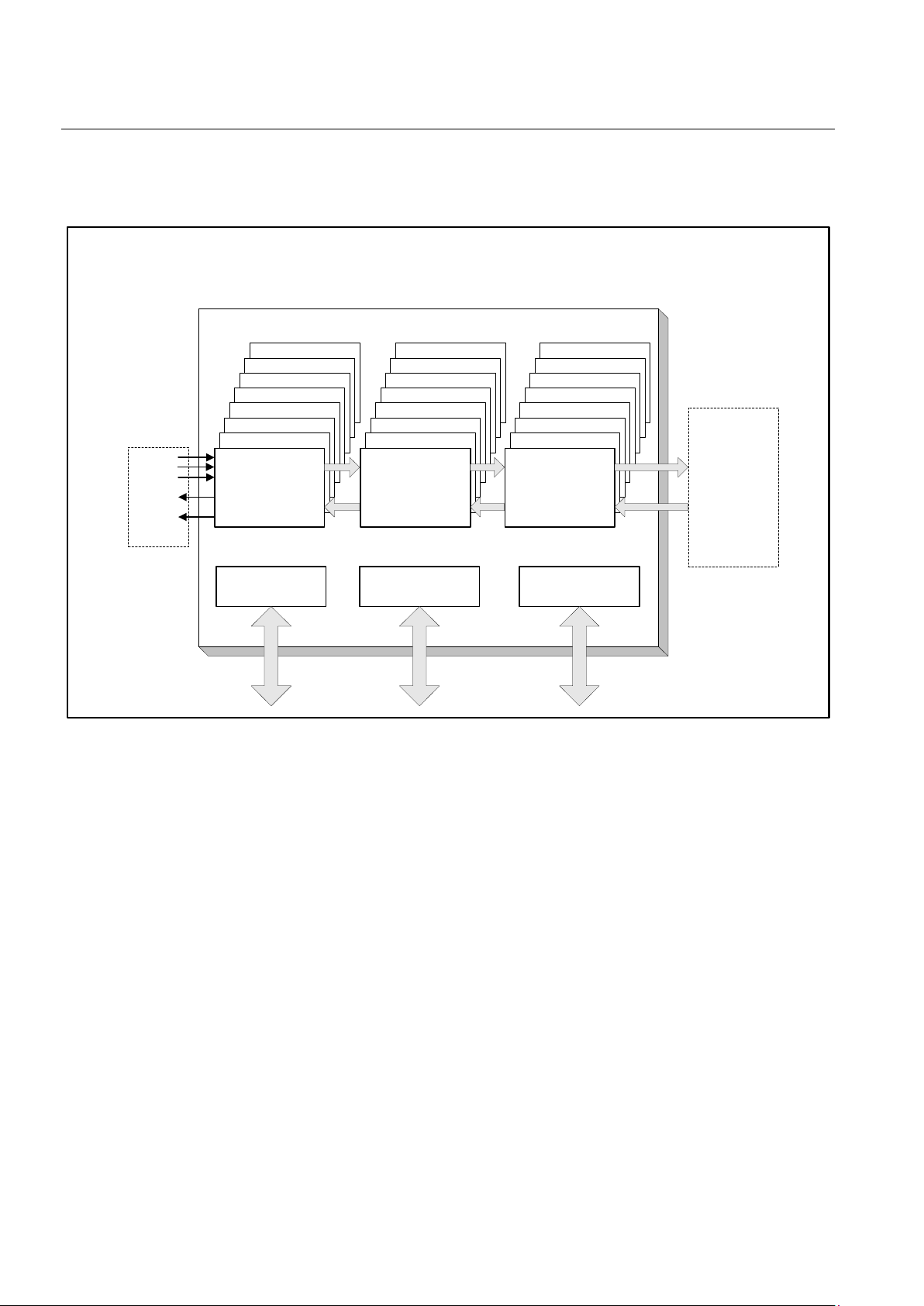
7. BLOCK DIAGRAMS
Figure 7-1. Block Diagram
x8
DS26518
FRAMER #8
FRAMER #7
FRAMER #6
...
FRAMER #4
FRAMER #3
FRAMER #2
T1/E1 FRAMER
HDLC
BERT
MICRO PROCESSOR
INTERFACE
JTAG PORT
CLOCK
GENERATION
LIU #8
LIU #7
LIU #6
...
LIU #4
LIU #3
LIU #2
LINE
INTERFACE
UNIT
INTERFACE #8
INTERFACE #7
INTERFACE #6
...
INTERFACE #4
INTERFACE #3
INTERFACE #2
BACKPLANE
INTERFACE
ELASTIC
STORES
RTIP
TRING
RRING
TTIP
CONTROLLER
PORT
TEST
PORT
CLOCK
ADAPTER
RECEIVE
BACKPLANE
SIGNALS
TRANSMIT
BACKPLANE
SIGNALS
HARDWARE
ALARM
INDICATORS
x8
RTIPE
Page 19
DS26518 8-Port T1/E1/J1 Transceiver
19 of 286
Figure 7-2. Detailed Block Diagram
CLOCK
SYNTHESIZ-
ER
MICROPROCESSOR
INTERFACE
JTAG
PORT
RESET
BLOCK
A[12:0]
D[7:0]
CSB
RDB/DSB
WRB/RWB
BTS
INTB
JTDI
JTMS
JTCLK
JTDO
JTRST
RESETB
MCLK
RCHBLK/CLKn
TCHBLK/CLKn
TCLKn
TSERn
TSYNCn/
TSSYNCIOn
TSYSCLKn
RSYSCLKn
RSYNCn
RSERn
RCLKn
BPCLK1
REFCLKIO
TTIPn
TRINGn
RRINGn
RTIPn
Serial Interface Mode:
SPI
(SCLK, CPOL, CPHA,
SWAP, MOSI, and MISO)
RSIGn
RM/RFSYNCn
TSIGn
PRE-SCALER
PLL
SPI_SEL
CLKO
TRANSMIT
LIU
Waveform
Shaper/Line
Driver
RECEIVE
LIU
Clock/Data
Recovery
JITTER ATTENUATOR
TRANSMIT
ENABLE
Tx
BERT
Rx
BERT
Tx
HDLC
Rx
HDLC
Tx FRAMER:
System IF
B8ZS/
HDB3
Encode
Elastic
Store
Rx FRAMER:
System IF
B8ZS/
HDB3
Decode
Elastic
Store
ALB
LLB
FLB
RLB
PLB
DS26518
TRANSCEIVER 1 OF 8
BACKPLANE INTERFACE
Page 20

DS26518 8-Port T1/E1/J1 Transceiver
20 of 286
8. PIN DESCRIPTIONS
8.1 Pin Functional Description
Table 8-1. Detailed Pin Descriptions
NAME PIN TYPE FUNCTION
ANALOG TRANSMIT
TTIP1 A1, A2
TTIP2 H1, H2
TTIP3 J1 J2
TTIP4 T1, T2
TTIP5 T15, T16
TTIP6 J15, J16
TTIP7 H15, H16
TTIP8 A15, A16
Analog
Output,
High
Impedance
Transmit Bipolar Tip for Transceiver 1 to 8. These pins are differential line
driver tip outputs. These pins can be high impedance if:
If TXENABLE is low, TTIPn/TRINGn will be high impedance. Note that if
TXENABLE is low, the register settings for control of TTIPn/TRINGn are ignored
and output is high impedance.
The differential outputs of TTIPn and TRINGn can provide internal matched
impedance for E1 75Ω, E1 120Ω, T1 100Ω, or J1 110Ω. The user can turn off
internal termination.
Note: The two pins shown for each transmit bipolar tip (e.g., pins A1 and A2 for
TTIP1) should be tied together.
TRING1 A3, B3
TRING2 G3, H3
TRING3 J3, K3
TRING4 R3, T3
TRING5 R14,T14
TRING6 J14, K14
TRING7 G14, H14
TRING8 A14, B14
Analog
Output,
High
Impedance
Transmit Bipolar Ring for Transceiver 1 to 8. These pins are differential line
driver ring outputs. These pins can be high impedance if:
If TXENABLE is low, TTIPn/TRINGn will be high impedance. Note that if
TXENABLE is low, the register settings for control of TTIPn/TRINGn are ignored
and output is high impedance.
The differential outputs of TTIPn and TRINGn can provide internal matched
impedance for E1 75Ω, E1 120Ω, T1 100Ω, or J1 110Ω. The user can turn off
internal termination.
Note: The two pins shown for each transmit bipolar ring (e.g., pins A3 and B3 for
TRING1) should be tied together.
TXENABLE/
SCAN_EN
L13 Input
Transmit Enable. If this pin is pulled low, all transmitter outputs (TTIPn and
TRINGn) are high impedance. The register settings for tri-state control of
TTIPn/TRINGn are ignored if TXENABLE is low. If TXENABLE is high, the
particular driver can be tri-stated by the register settings.
Scan Enable. When low, device is in normal operation. Scan enable is selected
by the SCANMODE pin. Note: User should not select scan enable—test mode
only.
ANALOG RECEIVE
RTIP1 C1
RTIP2 F1
RTIP3 L1
RTIP4 P1
RTIP5 P16
RTIP6 L16
RTIP7 F16
RTIP8 C16
Analog
Input
Receive Bipolar Tip for Transceiver 1 to 8. The differential inputs of RTIPn
and RRINGn can provide internal matched impedance for E1 75Ω, E1 120Ω, T1
100Ω, or J1 110Ω. The user can turn off internal termination via the LIU Receive
Impedance and Sensitivity Monitor register (
LRISMR).
RRING1 C2
RRING2 F2
RRING3 L2
RRING4 P2
RRING5 P15
RRING6 L15
RRING7 F15
RRING8 C15
Analog
Input
Receive Bipolar Ring for Transceiver 1 to 8. The differential inputs of RTIPn
and RRINGn can provide internal matched impedance for E1 75Ω, E1 120Ω, T1
100Ω, or J1 110Ω. The user has the option of turning off internal termination via
the LIU Receive Impedance and Sensitivity Monitor register (
LRISMR).
RESREF J5 Input
Resistor Reference. This pin is used to calibrate the internal impedance match
resistors of the receive LIUs. This pin should be tied to V
SS
through a 10kΩ ±1%
resistor.
Page 21

DS26518 8-Port T1/E1/J1 Transceiver
21 of 286
NAME PIN TYPE FUNCTION
TRANSMIT FRAMER
TSER1 F6
TSER2 E7
TSER3 R4
TSER4 N7
TSER5 M10
TSER6 L11
TSER7 F10
TSER8 D12
Input
Transmit NRZ Serial Data 1 to 8. These pins are sampled on the falling edge of
TCLKn when the transmit-side elastic store is disabled. These pins are sampled
on the falling edge of TSYSCLKn when the transmit-side elastic store is enabled.
In IBO mode, data for multiple framers can be used in high-speed multiplexed
scheme. This is described in Section
9.8.2. The table there presents the
combination of framer data for each of the streams.
TSYSCLKn is used as a reference when IBO is invoked. See Table 9-8.
TCLK1 C5
TCLK2 D7
TCLK3 P5
TCLK4 L8
TCLK5 L10
TCLK6 N11
TCLK7 E10
TCLK8 B13
Input
Transmit Clock 1 to 8. A 1.544MHz or a 2.048MHz primary clock. Used to clock
data through the transmit side of the transceiver. TSERn data is sampled on the
falling edge of TCLKn. TCLKn is used to sample TSERn when the elastic store is
not enabled or IBO is not used.
TSYSCLK1 P13 Input
Transmit System Clock 1. 1.544MHz, 2.048MHz, 4.096MHz, 8.192MHz, or
16.384MHz clock. Only used when the transmit-side elastic store function is
enabled. Should be tied low in applications that do not use the transmit-side
elastic store. The clock can be 4.096MHz, 8.912MHz, or 16.384MHz when IBO
mode is used. TSYSCLK1 does not have an internal pulldown resistor. Note: If
the
GTCR1.528MD bit is set, TSYSCLK1 becomes the master TSYSCLK for all
framers.
TSYSCLK2/
AL/RSIGF/FLOS2
F3
TSYSCLK3/
AL/RSIGF/FLOS3
L3
TSYSCLK4/
AL/RSIGF/FLOS4
P3
TSYSCLK5/
AL/RSIGF/FLOS5
P14
TSYSCLK6/
AL/RSIGF/FLOS6
L14
TSYSCLK7/
AL/RSIGF/FLOS7
F14
TSYSCLK8/
AL/RSIGF/FLOS8
C14
Input with
internal
pulldown/
Output
Transmit System Clock 2 to 8. 1.544MHz, 2.048MHz, 4.096MHz, 8.192MHz, or
16.384MHz clock. Only used when the transmit-side elastic store function is
enabled. Should be tied low in applications that do not use the transmit-side
elastic store. The clock can be 4.096MHz, 8.912MHz, or 16.384MHz when IBO
mode is used. TSYSCLK1 does not have an internal pulldown resistor. Note: If
the
GTCR1.528MD bit is set, TSYSCLK1 becomes the master TSYSCLK for all
framers.
Analog Loss/Receive-Signaling Freeze/Framer LOS. Analog LOS reflects the
LOS (loss of signal) detected by the LIU front-end and framer LOS is LOS
detection by the corresponding framer; the same pins can reflect receivesignaling freeze indications. This selection can be made by settings in the Global
Transceiver Clock Control Register 1 (
GTCCR1).
AL/RSIGF/FLOS[8:2] is available only by setting the
GTCR1.528MD bit to 1.
TSYNC1/
TSSYNCIO1
B4
TSYNC2/
TSSYNCIO2
F7
TSYNC3/
TSSYNCIO3
M6
TSYNC4/
TSSYNCIO4
M7
TSYNC5/
TSSYNCIO5
N10
TSYNC6/
TSSYNCIO6
T12
TSYNC7/
TSSYNCIO7
B11
TSYNC8/
TSSYNCIO8
A13
Input/
Output
Transmit Synchronization 1 to 8. A pulse at these pins establishes either frame
or multiframe boundaries for the transmit side. These signals can also be
programmed to output either a frame or multiframe pulse. If these pins are set to
output pulses at frame boundaries, they can also be set to output double-wide
pulses at signaling frames in T1 mode. The operation of these signals is
synchronous with TCLK[8:1].
Transmit System Synchronization In. These pins are selected when the
transmit-side elastic store is enabled. A pulse at these pins establishes either
frame or multiframe boundaries for the transmit side. Should be tied low in
applications that do not use the transmit-side elastic store. The operation of this
signal is synchronous with TSYSCLK[8:1].
Transmit System Synchronization Out. If configured as an output and the
transmit elastic store is enabled, an 8kHz pulse synchronous to the BPCLK1 will
be generated. This pulse in combination with BPCLK1 can be used as an IBO
master. TSSYNCIOn can be used as a source to RSYNCn and TSSYNCIOn of
another DS26518 or RSYNC and TSSYNC of other Dallas Semiconductor parts.
Note: TSSYNCIO[8:1] are not used when
GTCR1.528MD is set. When
GTCR1.528MD is set, the TSSYNCIO pin (N13) is used.
Page 22

DS26518 8-Port T1/E1/J1 Transceiver
22 of 286
NAME PIN TYPE FUNCTION
TSSYNCIO N13
Input/
Output
Note: In default operation, this pin is not used. When
GTCR1.528MD is set,
this pin is active. If pin is not used, tie low through a resistor.
Transmit System Synchronization In. This pin is selected when the transmitside elastic store is enabled. A pulse at this pin establishes either frame or
multiframe boundaries for the transmit side. Note that if the elastic store is
enabled, frame or multiframe boundary will be established for all transmitters.
Should be tied low in applications that do not use the transmit-side elastic store.
The operation of this signal is synchronous with TSYSCLKn.
Transmit System Synchronization Out. If configured as an output and the
transmit-side elastic store is enabled, an 8kHz pulse synchronous to BPCLK1 will
be generated. This pulse in combination with BPCLK1 can be used as an IBO
master. TSSYNCIO can be used as a source to RSYNCn and TSSYNCIO of
another DS26518 or RSYNC and TSSYNC of other Dallas Semiconductor parts.
TSIG1 D5
TSIG2 A6
TSIG3 T4
TSIG4 R6
TSIG5 T10
TSIG6 R12
TSIG7 A11
TSIG8 C13
Input
Transmit Signaling 1 to 8. When enabled, this input samples signaling bits for
insertion into outgoing PCM data stream. Sampled on the falling edge of TCLKn
when the transmit-side elastic store is disabled. Sampled on the falling edge of
TSYSCLKn when the transmit-side elastic store is enabled. In IBO mode, the
TSIGn streams can run up to 16.384MHz. See
Table 9-9.
TCHBLK1/
TCHCLK1
A5
TCHBLK2/
TCHCLK2
C7
TCHBLK3/
TCHCLK3
L7
TCHBLK4/
TCHCLK4
P7
TCHBLK5/
TCHCLK5
P9
TCHBLK6/
TCHCLK6
P11
TCHBLK7/
TCHCLK7
D10
TCHBLK8/
TCHCLK8
E11
Output
Transmit Channel Block/Transmit Channel Block Clock. A dual function pin.
TCHBLK[1:8]. TCHBLKn is a user-programmable output that can be forced high
or low during any of the channels. It is synchronous with TCLKn when the
transmit-side elastic store is disabled. It is synchronous with TSYSCLKn when
the transmit-side elastic store is enabled. It is useful for blocking clocks to a serial
UART or LAPD controller in applications where not all channels are used such as
Fractional T1, Fractional E1, 384kbps (H0), 768kbps, or ISDN-PRI. Also useful
for locating individual channels in drop-and-insert applications, for external per-
channel loopback, and for per-channel conditioning.
TCHCLK[1:8]. TCHCLKn is a 192kHz (T1) or 256kHz (E1) clock that pulses high
during the LSB of each channel. It can also be programmed to output a gated
transmit bit clock controlled by TCHBLKn. It is synchronous with TCLKn when the
transmit-side elastic store is disabled. It is synchronous with TSYSCLKn when
the transmit-side elastic store is enabled. Useful for parallel-to-serial conversion
of channel data.
Page 23

DS26518 8-Port T1/E1/J1 Transceiver
23 of 286
NAME PIN TYPE FUNCTION
RECEIVE FRAMER
RSER1 E5
RSER2 D6
RSER3 N4
RSER4 N6
RSER5 M11
RSER6 M12
RSER7 B12
RSER8 F11
Output
Received Serial Data 1 to 8. Received NRZ serial data. Updated on rising edges
of RCLKn when the receive-side elastic store is disabled. Updated on the rising
edges of RSYSCLKn when the receive-side elastic store is enabled.
When IBO mode is used, the RSERn pins can output data for multiple framers.
The RSERn data is synchronous to RSYSCLKn. See Section
9.8.2 and Table
9-6
.
RCLK1 F4
RCLK2 G4
RCLK3 L4
RCLK4 M4
RCLK5 K13
RCLK6 J13
RCLK7 F13
RCLK8 E13
Output
Receive Clock 1 to 8. A 1.544MHz (T1) or 2.048MHz (E1) clock that is used to
clock data through the receive-side framer. This clock is recovered from the
signal at RTIPn and RRINGn. RSERn data is output on the rising edge of
RCLKn. RCLKn is used to output RSERn when the elastic store is not enabled or
IBO is not used. When the elastic store is enabled or IBO is used, the RSERn is
clocked by RSYSCLKn.
RSYSCLK1 L12 Input
Receive System Clock 1. 1.544MHz, 2.048MHz, 4.096MHz, 8.192MHz, or
16.384MHz receive backplane clock. Only used when the receive-side elastic
store function is enabled. Should be tied low in applications that do not use the
receive-side elastic store. Multiple of 2.048MHz is expected when the IBO mode
is used. Note: If the
GTCR1.528MD bit is set, RSYSCLK1 becomes the master
RSYSCLK for all framers.
RSYSCLK2/
RLF/LTC2
E3
RSYSCLK3/
RLF/LTC3
M3
RSYSCLK4/
RLF/LTC4
N3
RSYSCLK5/
RLF/LTC5
N14
RSYSCLK6/
RLF/LTC6
M14
RSYSCLK7/
RLF/LTC7
E14
RSYSCLK8/
RLF/LTC8
D14
Input with
internal
pulldown/
Output
Receive System Clock 2 to 8. 1.544MHz, 2.048MHz, 4.096MHz, 8.192MHz, or
16.384MHz receive backplane clock. Only used when the receive-side elastic
store function is enabled. Should be tied low in applications that do not use the
receive-side elastic store. Multiple of 2.048MHz is expected when the IBO Mode
is used.
Receive Loss of Frame/Loss of Transmit Clock. This pin can also be
programmed to either toggle high when the synchronizer is searching for the
frame and multiframe or to toggle high if the TCLKn pin has not been toggled for
approximately three clock periods.
RLF/LTC[8:2] are available when
GTCR1.528MD = 1.
Note: If the GTCR1.528MD bit is set, RSYSCLK1 becomes the master
RSYSCLK for all framers.
RSYNC1 A4
RSYNC2 B6
RSYNC2 N5
RSYNC2 T6
RSYNC5 R10
RSYNC6 P12
RSYNC7 C11
RSYNC8 D13
Input/
Output
Receive Synchronization 1 to 8. If the receive-side elastic store is enabled, this
signal is used to input a frame or multiframe boundary pulse. If set to output
frame boundaries, RSYNCn can be programmed to output double-wide pulses on
signaling frames in T1 mode. In E1 mode, RSYNCn out can be used to indicate
CAS and CRC-4 multiframe. The DS26518 can accept an H.100-compatible
synchronization signal. The default direction of this pin at power-up is input, as
determined by the RSIO control bit in the
RIOCR.2 register.
Page 24

DS26518 8-Port T1/E1/J1 Transceiver
24 of 286
NAME PIN TYPE FUNCTION
RMSYNC1/
RFSYNC1
C4
RMSYNC2/
RFSYNC2
C6
RMSYNC3/
RFSYNC3
P4
RMSYNC4/
RFSYNC4
P6
RMSYNC5/
RFSYNC5
P10
RMSYNC6/
RFSYNC6
N12
RMSYNC7/
RFSYNC7
D11
RMSYNC8/
RFSYNC8
E12
Output
Receive Multiframe/Frame Synchronization 1 to 8. A dual function pin to
indicate frame or multiframe synchronization. RFSYNCn is an extracted 8kHz
pulse, one RCLKn wide that identifies frame boundaries. RMSYNCn is an
extracted pulse, one RCLKn wide (elastic store disabled) or one RSYSCLKn wide
(elastic store enabled), that identifies multiframe boundaries. When the receive
elastic store is enabled, the RMSYNCn signal indicates the multiframe sync on
the system (backplane) side of the elastic store. In E1 mode, this pin can indicate
either the CRC-4 or CAS multiframe as determined by the RSMS2 control bit in
the Receive I/O Configuration register (
RIOCR.1).
RSIG1 D4
RSIG2 E6
RSIG3 M5
RSIG4 R5
RSIG5 R11
RSIG6 R13
RSIG7 A12
RSIG8 F12
Output
Receive Signaling 1 to 8. Outputs signaling bits in a PCM format. Updated on
rising edges of RCLKn when the receive-side elastic store is disabled. Updated
on the rising edges of RSYSCLKn when the receive-side elastic store is enabled.
See
Table 9-7.
RCHBLK1/
RCHCLK1
E4
RCHBLK2/
RCHCLK2
B5
RCHBLK3/
RCHCLK3
L6
RCHBLK4/
RCHCLK4
T5
RCHBLK5/
RCHCLK5
T11
RCHBLK6/
RCHCLK6
T13
RCHBLK7/
RCHCLK7
C12
RCHBLK8/
RCHCLK8
G13
Output
Receive Channel Block/Receive Channel Block Clock. This pin can be
configured to output either RCHBLK or RCHCLK.
RCHBLK[1:8]. RCHBLKn is a user-programmable output that can be forced high
or low during any of the 24 T1 or 32 E1 channels. It is synchronous with RCLKn
when the receive-side elastic store is disabled. It is synchronous with RSYSCLKn
when the receive-side elastic store is enabled. This pin is useful for blocking
clocks to a serial UART or LAPD controller in applications where not all channels
are used such as fractional service, 384kbps service, 768kbps, or ISDN-PRI.
Also useful for locating individual channels in drop-and-insert applications, for
external per-channel loopback, and for per-channel conditioning.
RCHCLK[1:8]. RCHCLKn is a 192kHz (T1) or 256kHz (E1) clock that pulses high
during the LSB of each channel. It is synchronous with RCLKn when the receive-
side elastic store is disabled. It is synchronous with RSYSCLKn when the
receive-side elastic store is enabled. It is useful for parallel-to-serial conversion of
channel data.
BPCLK1 E8 Output
Backplane Clock 1. Programmable clock output that can be set to 2.048MHz,
4.096MHz, 8.192MHz, or 16.384MHz. The reference for this clock can be
RCLK[8:1], a 1.544MHz or 2.048MHz clock frequency derived from MCLK, or an
external reference clock (REFCLKIO). This allows system clocks to be
referenced from external sources, the T1J1E1 recovered clocks, or the MCLK
oscillator.
CLKO/
RLF/LTC1
D3 Output
Clock Out. Clock output pin that can be programmed to output numerous
frequencies referenced to MCLK. Frequencies available: 1.544MHz, 2.048MHz,
4.096MHz, 8.192MHz, 12.288MHz, 16.384MHz, 256kHz, and 64kHz.
GTCCR3.CLKOSEL[2:0] selects the frequency.
Receive Loss of Frame/Loss of Transmit Clock. This pin can also be
programmed to either toggle high when the synchronizer is searching for the
frame and multiframe, or to toggle high if the TCLKn pin has not been toggled for
approximately three clock periods.
RLF/LTC1 is available on the DS26518 when
GTCR1.528MD = 1.
Page 25

DS26518 8-Port T1/E1/J1 Transceiver
25 of 286
NAME PIN TYPE FUNCTION
MICROPROCESSOR INTERFACE
A12 C8
A11 A8
A10 B8
A9 F8
A8 B9
A7 A9
A6 C9
A5 D9
A4 E9
A3 F9
A2 B10
A1 A10
A0 C10
Input
Address [12:0]. This bus selects a specific register in the DS26518 during
read/write access. A12 is the MSB and A0 is the LSB.
D[7]/SPI_CPOL T9
Input/
Output
Data [7]/SPI Interface Clock Polarity
D[7]: Bit 7 of the 16-bit or 8-bit data bus used to input data during register writes
and data outputs during register reads. Not driven when CSB = 1.
SPI_CPOL: This signal selects the clock polarity when SPI_SEL = 1. See Section
9.1.2 for detailed timing and functionality information. Default setting is low.
D[6]/SPI_CPHA N9
Input/
Output
Data [6]/SPI Interface Clock Phase
D[6]: Bit 6 of the 16-bit or 8-bit data bus used to input data during register writes
and data outputs during register reads. Not driven when CSB = 1.
SPI_CPHA: This signal selects the clock phase when SPI_SEL = 1. See Section
9.1.2 for detailed timing and functionality information. Default setting is low.
D[5]/SPI_SWAP M9
Input/
Output
Data [5]/SPI Bit Order Swap
D[5]: Bit 5 of the 16-bit or 8-bit data bus used to input data during register writes
and data outputs during register reads. Not driven when CSB = 1.
SPI_SWAP: This signal is active when SPI_SEL = 1. The address and data bit
order is swapped when SPI_SWAP is high. The R/W and B bit positions are
never changed in the control word.
0 = LSB is transmitted and received first.
1 = MSB is transmitted and received first.
D[4] R8
Input/
Output
Data [4]. Bit 4 of the 8-bit data bus used to input data during register writes and
data outputs during register reads. Not driven when CSB = 1.
D[3] T8
Input/
Output
Data [3]. Bit 3 of the 8-bit data bus used to input data during register writes and
data outputs during register reads. Not driven when CSB = 1.
D[2]/SPI_SCLK P8
Input/
Output
Data [2]/SPI Serial Interface Clock
D[2]: Bit 2 of the 8-bit data bus used to input data during register writes and data
outputs during register reads. Not driven when CSB = 1.
SPI_SCLK: SPI Serial Clock Input when SPI_SEL = 1.
D[1]/SPI_MOSI L9
Input/
Ouput
Data [1]/SPI Serial Interface Data Master Out-Slave In
D[1]: Bit 1 of the 8-bit data bus used to input data during register writes, and data
outputs during register reads. Not driven when CSB = 1.
SPI_MOSI: SPI Serial Data Input (Master Out-Slave In) when SPI_SEL = 1.
D[0]/SPI_MISO N8
Input/
Output
Data [0]/SPI Serial Interface Data Master In-Slave Out
D[0]: Bit 0 of the 8-bit data bus used to input data during register writes and data
outputs during register reads. Not driven when CSB = 1.
SPI_MISO: SPI Serial Data Output (Master In-Slave Out) when SPI_SEL = 1.
CSB
T7 Input
Chip-Select Bar. This active-low signal is used to qualify register read/write
accesses. The RDB/DSB and WRB signals are qualified with CSB.
RDB/
DSB
M8 Input
Read-Data Bar/Data-Strobe Bar. This active-low signal along with CSB qualifies
read access to one of the DS26518 registers. The DS26518 drives the data bus
with the contents of the addressed register while RDB and CSB are low.
Page 26

DS26518 8-Port T1/E1/J1 Transceiver
26 of 286
NAME PIN TYPE FUNCTION
WRB/
RWB
R7 Input
Write-Read Bar/Read-Write Bar. This active-low signal along with CSB qualifies
write access to one of the DS26518 registers. Data at D[7:0] is written into the
addressed register at the rising edge of WRB while CSB is low.
INTB
R9
Output,
Tri-
Stateable
Interrupt Bar. This active-low output is asserted when an unmasked interrupt
event is detected. INTB will be deasserted (and tri-stated) when all interrupts
have been acknowledged and serviced. Extensive mask bits are provided at the
global level, framer, LIU, and BERT level.
SPI_SEL/
AL/RSIGF/FLOS1
C3
Input with
internal
pulldown/
Output
SPI Serial Bus Mode Select/Analog Loss/Receive Signaling Freeze/Framer
LOS
SPI_SEL: 0 = Parallel Bus Mode, 1 = SPI Serial Bus Mode
AL/RSIGF/FLOS1: Analog LOS reflects the loss of signal detected by the LIU
front-end; framer LOS is LOS detection by the corresponding framer. The same
pins can reflect receive-signaling freeze indications. This selection can be made
by settings in Global Transceiver Control Register (
GTCR1). AL/RSIGF/FLOS1
are available by setting the
GTCR1.528MD bit to 1.
BTS M13 Input
Bus Type Select. Set high to select Motorola bus timing, low to select Intel bus
timing. This pin controls the function of the RDB/DSB and WRB pins. Note: If SPI
mode is selected by the SPI_SEL pin, this pin must be tied low.
SYSTEM INTERFACE
MCLK B7 Input
Master Clock. This is an independent free-running clock whose input can be a
multiple of 2.048MHz ±50ppm or 1.544MHz ±50ppm. The clock selection is
available by bits MPS0 and MPS1 and FREQSEL. Multiple of 2.048MHz can be
internally adapted to 1.544MHz. Multiple of 1.544MHz can be adapted to
2.048MHz. Note that TCLKn must be 2.048MHz for E1 and 1.544MHz for T1/J1
operation. See
Table 10-12.
RESETB
J12 Input
Reset Bar. Active-low reset. This input forces the complete DS26518 reset. This
includes reset of the registers, framers, and LIUs.
REFCLKIO A7
Input/
Output
Reference Clock Input/Output
Input: A 2.048MHz or 1.544MHz clock input. This clock can be used to generate
the backplane clock. This allows for the users to synchronize the system
backplane with the reference clock. The other options for the backplane clock
reference are LIU-received clocks or MCLK.
Output: This signal can also be used to output a 1.544MHz or 2.048MHz
reference clock. This allows for multiple DS26518s to share the same reference
for generation of the backplane clock. Hence, in a system consisting of multiple
DS26518s, one can be a master and others a slave using the same reference
clock.
TEST
DIGIOEN D8
Input,
Pullup
Digital Enable. When this pin and JTRST are pulled low, all digital I/O pins are
placed in a high-impedance state. If this pin is high the digital I/O pins operate
normally. This pin must be connected to V
DD
for normal operation.
JTRST
L5
Input,
Pullup
JTAG Reset. JTRST is used to asynchronously reset the test access port
controller. After power-up, JTRST must be toggled from low to high. This action
sets the device into the JTAG DEVICE ID mode. Pulling JTRST low restores
normal device operation. JTRST is pulled high internally via a 10kΩ resistor
operation. If boundary scan is not used, this pin should be held low.
JTMS K4
Input,
Pullup
JTAG Mode Select. This pin is sampled on the rising edge of JTCLK and is used
to place the test access port into the various defined IEEE 1149.1 states. This pin
has a 10kΩ pullup resistor.
JTCLK F5 Input
JTAG Clock. This signal is used to shift data into JTDI on the rising edge and out
of JTDO on the falling edge.
JTDI H4
Input,
Pullup
JTAG Data In. Test instructions and data are clocked into this pin on the rising
edge of JTCLK. This pin has a 10kΩ pullup resistor.
JTDO J4
Output,
High
Impedance
JTAG Data Out. Test instructions and data are clocked out of this pin on the
falling edge of JTCLK. If not used, this pin should be left unconnected.
Page 27

DS26518 8-Port T1/E1/J1 Transceiver
27 of 286
NAME PIN TYPE FUNCTION
SCANMODE H13 Input
Scan Mode. When low, normal operational clocks are used to clock the flip flops.
User should tie low.
POWER SUPPLIES
ATVDD
B1, B16,
G1, G16,
K1, K16,
R1, R16
—
3.3V ±5% Analog Transmit Power Supply. These V
DD
inputs are used for the
transmit LIU sections of the DS26518.
ATVSS
B2, B15,
G2, G15,
K2, K15,
R2, R15
—
Analog Transmit VSS. These pins are used for transmit analog VSS.
ARVDD
D1, D16,
E1, E16,
M1, M16,
N1, N16
—
3.3V ±5% Analog Receive Power Supply. These V
DD
inputs are used for the
receive LIU sections of the DS26518.
ARVSS
D2, D15,
E2, E15,
M2, M15,
N2, N15
—
Analog Receive V
SS
. These pins are used for analog VSS for the receivers.
ACVDD H7 —
1.8V ±5% Analog Clock Conversion V
DD
. This VDD input is used for the clock
conversion unit (CLAD) of the DS26518.
ACVSS J7 —
Analog Clock V
SS
. This pin is used for clock converter analog VSS.
DVDD33
G5, G6,
G11, G12,
H5, H6,
H8, H9,
H10, H11
—
3.3V ±5% Power Supply for I/Os
DVDD18 G7–G10 —
1.8V ±5% Power Supply for Internal V
DD
DVSS
H12, J6,
J8–J11,
K5–K12
—
Digital Ground
Page 28

DS26518 8-Port T1/E1/J1 Transceiver
28 of 286
9. FUNCTIONAL DESCRIPTION
9.1 Processor Interface
Microprocessor control of the DS26518 is accomplished through the 28 hardware pins of the microprocessor port.
The 8-bit parallel data bus can be configured for Intel or Motorola modes of operation with the bus type select
(BTS) pin. When the BTS pin is a logic 0, bus timing is in Intel mode, as shown in
Figure 13-2 and Figure 13-3.
When the BTS pin is a logic 1, bus timing is in Motorola mode, as shown in
Figure 13-4 and Figure 13-5. The
address space is mapped through the use of 13 address lines, A[12:0]. Multiplexed mode is not supported on the
processor interface.
The chip-select bar (CSB) pin must be brought to a logic-low level to gain read and write access to the
microprocessor port. With Intel timing selected, the read-data bar (RDB) and write-read bar (WRB) pins are used to
indicate read and write operations and latch data through the interface. With Motorola timing selected, the readwrite bar (RWB) pin is used to indicate read and write operations while the data-strobe bar (DSB) pin is used to
latch data through the interface.
The interrupt output pin (INTB) is an open-drain output that asserts a logic-low level upon a number of software
maskable interrupt conditions. This pin is normally connected to the microprocessor interrupt input.
9.1.1 SPI Serial Port Mode
The external processor bus can be configured to operate in SPI serial bus mode. See Section 9.1.2 for detailed
timing diagrams.
When SPI_SEL = 1, SPI bus mode is implemented using four signals: clock (SPI_SCLK), master out-slave in data
(SPI_MOSI), master in-slave out data (SPI_MISO), and chip select (CSB). Clock polarity and phase can be set by
the D[7]/SPI_CPOL and D[6]/SPI_CPHA pins.
The order of the address and data bits in the serial stream is selectable using the D[5]/SPI_SWAP pin. The R/W bit
is always first and B bit is always last in the initial control word and are not effected by the D[5]/SPI_SWAP pin
setting.
SPI mode is not recommended for HDLC operations because of the bandwidth constraints of SPI.
9.1.2 SPI Functional Timing Diagrams
Note: The transmit and receive order of the address and data bits are selected by the D[5]/SPI_SWAP pin. The
R/W (read/write) MSB bit and B (burst) LSB bit position is not affected by the D[5]/SPI_SWAP pin setting.
9.1.2.1 SPI Transmission Format and CPHA Polarity
When SPI_CPHA = 0, CSB may be deasserted between accesses. An access is defined as one or two control
bytes followed by a data byte. CSB cannot be deasserted between the control bytes, or between the last control
byte and the data byte. When SPI_CPHA = 0, CSB may also remain asserted between accesses. If it remains
asserted and the BURST bit is set, no additional control bytes are expected after the first control byte(s) and data
are transferred. If the BURST bit is set, the address will be incremented for each additional byte of data transferred
until CSB is deasserted. If CSB remains asserted and the BURST bit is not set, a control byte(s) is expected
following the data byte, and the address for the next access will be received from that. Anytime CSB is deasserted,
the BURST access is terminated.
When SPI_CPHA = 1, CSB may remain asserted for more than one access without being toggled high and then
low again between accesses. If the BURST bit is set, the address should increment and no additional control bytes
are expected. If the BURST bit is not set, each data byte will be followed by the control byte(s) for the next access.
Additionally, CSB may also be deasserted between accesses when SPI_CPHA = 1. In the case, any BURST
access is terminated and the next byte received when CSB is reasserted will be a control byte.
The following diagrams describe the functionality of the SPI port for the four combinations of SPI_CPOL and
SPI_CPHA. They indicate the clock edge that samples the data and the level of the clock during no-transfer events
(high or low). Since the SPI port of the DS26518 acts as a slave device, the master device provides the clock. The
Page 29
DS26518 8-Port T1/E1/J1 Transceiver
29 of 286
user must configure the SPI_CPOL and SPI_CPHA pins to describe which type of clock that the master device is
providing.
Figure 9-1. SPI Serial Port Access for Read Mode, SPI_CPOL = 0, SPI_CPHA = 0
1
A7
A13 A12 A11 A10 A9 A8
D7 D6 D5 D4 D3 D2 D1 D0
LSBMSB
LSB
MSB
SPI_SCLK
C
SB
SPI_MOSI
SPI_MISO
B
A6 A5 A4 A3 A2 A1
LSBMSB
A0
Figure 9-2. SPI Serial Port Access for Read Mode, SPI_CPOL = 1, SPI_CPHA = 0
SPI_SCLK
1
A7
A13 A12 A11 A10 A9 A8
D7 D6 D5 D4 D3 D2 D1 D0
LSBMSB
LSB
MSB
SPI_MOSI
SPI_MISO
B
A6 A5 A4 A3 A2 A1
LSBMSB
A0
C
SB
Figure 9-3. SPI Serial Port Access for Read Mode, SPI_CPOL = 0, SPI_CPHA = 1
SPI_SCLK
CSB
1
A
7
A
13
A
12
A
11
A
10
A
9
A
8
D7 D6 D5 D4 D3 D2 D1 D0
LSBMSB
LSB
MSB
SPI_MOSI
SPI_MISO
B
A6A5A4A3A2A
1
LSBMSB
A
0
Figure 9-4. SPI Serial Port Access for Read Mode, SPI_CPOL = 1, SPI_CPHA = 1
SPI_SLCK
CSB
1
A
7
A
13
A
12
A
11
A
10
A
9
A
8
D7 D6 D5 D4 D3 D2 D1 D0
LSBMSB
LSB
MSB
SPI_MOSI
SPI_MISO
B
A6A5A4A3A2A
1
LSBMSB
A
0
Page 30
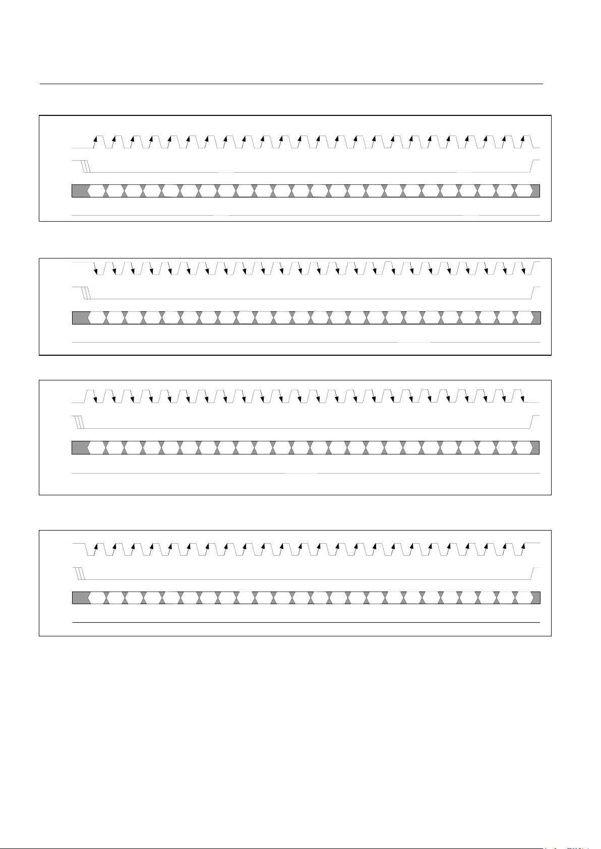
DS26518 8-Port T1/E1/J1 Transceiver
30 of 286
Figure 9-5. SPI Serial Port Access for Write Mode, SPI_CPOL = 0, SPI_CPHA = 0
0
A
13
LSB
MSB
SPI_SCLK
CSB
SPI_MOSI
SPI_MISO
D7 D6 D5 D4 D3 D2 D1 D0
LSBMSB
A4A3A2A1A
0
LSBMSB
A
12
A
11
A
10
A
9
A
8
A
7
A6A
5
B
Figure 9-6. SPI Serial Port Access for Write Mode, SPI_CPOL = 1, SPI_CPHA = 0
SPI_SCLK
CSB
0
A
13
LSB
MSB
SPI_MOSI
SPI_MISO
D7 D6 D5 D4 D3 D2 D1 D0
LSBMSB
A4A3A2A1A
0
LSBMSB
A
12
A
11
A
10
A
9
A
8
A
7
A6A
5
B
Figure 9-7. SPI Serial Port Access for Write Mode, SPI_CPOL = 0, SPI_CPHA = 1
SPI_SCL
K
CSB
0
A
13
LSB
MSB
SPI_MOSI
SPI_MISO
D7 D6 D5 D4 D3 D2 D1 D0
LSBMSB
A4A3A2A1A
0
LSBMSB
A
12
A
11
A
10
A
9
A
8
A
7
A6A
5
B
Figure 9-8. SPI Serial Port Access for Write Mode, SPI_CPOL = 1, SPI_CPHA = 1
SPI_SCLK
CSB
0
A
13
LSB
MSB
SPI_MOSI
SPI_MISO
D7 D6 D5 D4 D3 D2 D1 D0
LSBMSB
A4A3A2A1A
0
LSBMSB
A
12
A
11
A
10
A
9
A
8
A
7
A6A
5
B
Page 31

DS26518 8-Port T1/E1/J1 Transceiver
31 of 286
9.2 Clock Structure
The user should provide a system clock to the MCLK input of 2.048MHz, 1.544MHz, or a multiple of up to 8x the T1
and E1 frequencies. To meet many specifications, the MCLK source should have ±50ppm accuracy.
9.2.1 Backplane Clock Generation
The DS26518 provides facility for provision of BPCLK1 at 2.048MHz, 4.096MHz, 8.192MHz, 16.384MHz (see
Figure 9-9). The Global Transceiver Clock Control Register 1 (GTCCR1) is used to control the backplane clock
generation. This register is also used to program REFCLKIO as an input or output. REFCLKIO can be an output
sourcing MCLKT1 or MCLKE1 as shown in
Figure 9-9.
This backplane clock and frame pulse (TSSYNCIOn) can be used by the DS26518 and other IBO-equipped
devices as an “IBO Bus Master.” Hence, the DS26518 provides the 8kHz sync pulse and 4MHz, 8MHz, and 16MHz
clock. This can be used by the link layer devices and frames connected to the IBO bus.
Figure 9-9. Backplane Clock Generation
Clock
Multiplexor
RCLK3
RCLK4
RCLK5
RCLK6
RCLK7
RCLK1
RCLK2
Pre
Scaler
PLL
MCLKT1
MCLKE1
MCLK
BPREFSEL3:0
CLK
GEN
REFCLKIO
REFCLKIO
BPCLK
BPCLK1:0
BFREQSEL
TSSYNCIO
RCLK8
The reference clock for the backplane clock generator can be as follows:
• External Master Clock. A prescaler can be used to generate T1 or E1 frequency.
• External Reference Clock REFCLKIO. This allows for multiple DS26518s to use the backplane clock from
a common reference.
• Internal LIU recovered RCLKs 1 to 8.
• The clock generator can be used to generate BPCLK1 of 2.048MHz, 4.096MHz, 8.192MHz, or 16.384MHz
for the IBO.
• If MCLK or RCLKn is used as a reference, REFCLKIO can be used to provide a 2.048MHz or 1.544MHz
clock for external use.
Page 32

DS26518 8-Port T1/E1/J1 Transceiver
32 of 286
9.2.2 CLKO Output Clock Generation
This clock output is derived from MCLK based upon the setting of the CLKOSEL[2:0] bits in the GTCCR3
register.The reference for the PLL is not the input clock on MCLK, but the scaled version of MCLK (1.544MHz or
2.048MHz). The
LTRCR.T1J1E1S bit also selects the proper PLL for use in generating the appropriate frequency.
This clock output pin is provided as an additional feature to eliminate the need for another board oscillator.
Table 9-1. CLKO Frequency Selection
CLKOSEL[3:0] CLKO (kHz)
0000 2048
0001 4096
0010 8192
0011 16384
0100 1544
0101 3088
0110 6176
0111 12352
1000 1536
1001 3072
1010 6144
1011 12288
1100 32
1101 64
1110 128
1111 256
Page 33

DS26518 8-Port T1/E1/J1 Transceiver
33 of 286
9.3 Resets and Power-Down Modes
A hardware reset is issued by forcing the RESETB pin to logic low. The RESETB input pin resets all framers, LIUs,
and BERTs. Note that not all registers are cleared to 00h on a reset condition. The register space must be
reinitialized to appropriate values after a hardware or software reset has occurred. This includes writing
reserved locations to 00h.
Table 9-2. Reset Functions
RESET FUNCTION LOCATION COMMENTS
Hardware Device Reset
RESETB Pin
Transition to a logic 0 level resets the DS26518.
Hardware JTAG Reset
JTRST Pin
Resets the JTAG test port.
Global Software Reset GSRR1
Writing to this register resets the framers, LIUs and BERTs
(transmit and receive).
Framer Receive Reset RMMR.1 Writing to this bit resets the receive framer.
Framer Transmit Reset TMMR.1 Writing to this bit resets the transmit framer.
HDLC Receive Reset RHC.6 Writing to this bit resets the receive HDLC controller.
HDLC Transmit Reset THC1.5 Writing to this bit resets the transmit HDLC controller.
Elastic Store Receive Reset RESCR.2 Writing to this bit resets the receive elastic store.
Elastic Store Transmit Reset TESCR.2 Writing to this bit resets the transmit elastic store.
Bit Oriented Code Receive
Reset
T1RBOCC.7 Writing to this bit resets the receive BOC controller.
Loop Code Integration Reset
T1RDNCD1,
T1RUPCD1
Writing to these registers resets the programmable in-band
code integration period.
Spare Code Integration Reset T1RSCD1
Writing to this register resets the programmable in-band
code integration period.
The DS26518 has several features included to reduce power consumption. The individual LIU transmitters can be
powered down by setting the TPDE bit in the LIU Maintenance Control Register (
LMCR). Note that powering down
the transmit LIU results in a high-impedance state for the corresponding TTIPn and TRINGn pins and reduced
operating current. The RPDE in the
LMCR register can be used to power down the LIU receiver.
The TE (transmit enable) bit in the
LMCR register can be used to disable the TTIPn and TRINGn outputs and place
them in a high-impedance mode, while keeping the LIU in an active state (powered up). This is useful for
equipment protection-switching applications.
Page 34

DS26518 8-Port T1/E1/J1 Transceiver
34 of 286
9.4 Initialization and Configuration
9.4.1 Example Device Initialization and Sequence
STEP 1: Reset the device by pulling the RESETB pin low, applying power to the device, or by using the software
reset bits outlined in Section
9.2.2. Clear all reset bits. Allow time for the reset recovery.
STEP 2: Check the Device ID in the
IDR register.
STEP 3: Write the
GTCCR1 register to correctly configure the system clocks. If supplying a 1.544MHz MCLK
follows this write with at least a 300ns delay in order to allow the clock system to properly adjust.
STEP 4: Write the entire remainder of the register space for each port with 00h, including reserved register
locations.
STEP 5: Choose T1/J1 or E1 operation for the framers by configuring the T1/E1 bit in the
TMMR and RMMR
registers for each framer. Set the FRM_EN bit to 1 in the
TMMR and RMMR registers. If using software transmit
signaling in E1 mode, program the
E1TAF and E1TNAF registers as required. Configure the framer Transmit
Control Registers (
TCR1–TCR4). Configure the framer Receive Control Registers (RCR1–RCR3). Configure other
framer features as appropriate.
STEP 6: Choose T1/J1 or E1 operation for the LIUs by configuring the T1J1E1S bit in the
LTRCR register.
Configure the line build-out for each LIU. Configure other LIU features as appropriate. Set the TE (transmit enable)
bit to turn on the TTIPn and TRINGn outputs.
STEP 7: Configure the elastic stores, HDLC controller, and BERT as needed.
STEP 8: Set the INIT_DONE bit in the
TMMR and RMMR registers for each framer.
9.5 Global Resources
All eight framers share a common microprocessor port and a common MCLK. There is a common software
configurable BPCLK1 output. A set of global registers includes global resets, global interrupt status, interrupt
masking, clock configuration, and the device ID register. See the global register bit map in
Table 10-6. A common
JTAG controller is used for all ports.
9.6 Per-Port Resources
Each port has an associated framer, LIU, BERT, jitter attenuator, and transmit/receive HDLC controller. Each of the
per-port functions has its own register space.
9.7 Device Interrupts
Figure 9-10 diagrams the flow of interrupt conditions from their source status bits through the multiple levels of
information registers and mask bits to the interrupt pin. When an interrupt occurs, the host can read the global
interrupt information registers
GFISR1, GLISR1, and GBISR1 to quickly identify which of the eight transceivers is
(are) causing the interrupt(s). The host can then read the specific transceiver’s interrupt information registers (
TIIR,
RIIR) and the latched status registers (LLSR, BLSR) to further identify the source of the interrupt(s). If TIIR or RIIR
is the source, the host reads the transmit latched status or the receive latched status registers for the source of the
interrupt. All interrupt information register bits are real-time bits that clear once the appropriate interrupt has been
serviced and cleared, as long as no additional, unmasked interrupt condition is present in the associated status
register. All latched status bits must be cleared by the host writing a “1” to the bit location of the interrupt condition
that has been serviced. Latched status bits that have been masked via the interrupt mask registers are masked
from the interrupt information registers. The interrupt mask register bits prevent individual latched status conditions
from generating an interrupt, but they do not prevent the latched status bits from being set. Therefore, when
servicing interrupts, the user should XOR the latched status with the associated interrupt mask in order to exclude
bits for which the user wished to prevent interrupt service. This architecture allows the application host to
periodically poll the latched status bits for noninterrupt conditions, while using only one set of registers.
Page 35

DS26518 8-Port T1/E1/J1 Transceiver
35 of 286
Figure 9-10. Device Interrupt Information Flow Diagram
Receive Remote Alarm Indication Clear 7
Receive Alarm Condition Clear 6
Receive Loss of Signal Clear 5
Receive Loss of Frame Clear 4
Receive Remote Alarm Indication 3
Receive Alarm Condition 2
Receive Loss of Signal 1
Receive Loss of Frame 0
RLS1
RIM1
Receive Signal All Ones 3
Receive Signal All Zeros 2
Receive CRC4 Multiframe 1
Receive Align Frame 0
RLS
2
RIM2
Loss of Receive Clk Clear / Loss of Receive Clk Clear 7
Spare Code Detected Condition Clear / - 6
Loop Down Code Clear / V52 Link Clear 5
Loop Up Code Clear / Receive Distant MF Alarm Clear 4
Loss of Receive Clk / Loss of Receive Clk 3
Spare Code Detect / - 2
Loop Down Detect / V52 Link Detect 1
Loop Up Detect / Receive Distant MF Alarm Detect 0
RLS3
RIM3
Receive Elastic Store Full 7
Receive Elastic Store Empty 6
Receive Elastic Store Slip 5
Receive Signaling Change of State (Enable in RSCSE1-4) 3
One Second Timer 2
Timer 1
Receive Multiframe 0
RLS4
RIM4
Receive FIFO Overrun 5
Receive HDLC Opening Byte 4
Receive Packet End 3
Receive Packet Start 2
Receive Packet High Watermark 1
Receive FIFO Not Empty 0
RLS5
RIM5
Receive RAI-CI 5
Receive AIS-CI 4
Receive SLC-96 Alignment 3
Receive FDL Register Full 2
Receive BOC Clear 1
Receive BOC 0
RLS7
RIM7
Transmit Elastic Store Full 7
Transmit Elastic Store Empty 6
Transmit Elastic Store Slip 5
Transmit SLC96 Multiframe 4
Transmit Align Frame 3
Transmit Multiframe 2
Loss of Transmit Clock Clear 1
Loss of Transmit Clock 0
TLS1
TIM1
Transmit FDL Register Empty 4
Transmit FIFO Underrun 3
Transmit Message End 2
Transmit FIFO Below Low Watermark 1
Transmit FIFO Not Full Set 0
TLS2
TIM2
- -
- Loss of Frame 1
Loss of Frame Synchronization 0
TLS3
TIM3
Jitter Attenuator Limit Trip Clear 7
Open Circuit Detect Clear 6
Short Circuit Detect Clear 5
Loss of Signal Detect Clear 4
Jitter Attenuator Limit Trip 3
Open Circuit Detect 2
Short Circuit Detect 1
Loss of Signal Detect 0
LLSR
LSIMR
BERT Bit Error Detected 6
BERT Bit Counter Overflow 5
BERT Error Counter Overflow 4
BERT Receive All Ones 3
BERT Receive All Zeros 2
BERT Receive Loss of Synchronization 1
BERT in Synchronization 0
BLSR
BSIM
Interrupt Pin
0
1
2
3
4
5
RIIR
2
1
0
TIIR
6
5
4
3
2
1
0
GFISR1
GFIMR1
GLISR1
GLIMR1
GBISR1
GBIMR1
GTCR1.0
Framers 2-8 LIUs 2-8 BERTs 2-8
Drawing Legend:
Interrupt Status
Registers
Register Name
Interrupt Mask
Registers
Register Name
Page 36

DS26518 8-Port T1/E1/J1 Transceiver
36 of 286
9.8 System Backplane Interface
The DS26518 provides a versatile backplane interface that can be configured to:
• Transmit and receive two-frame elastic stores
• Mapping of T1 channels into a 2.048MHz backplane
• IBO mode for multiple framers to share the backplane signals
• Transmit and receive channel blocking capability
• Fractional T1/E1/J1 support
• Hardware-based (through the backplane interface) or processor-based signaling
• Flexible backplane clock providing frequencies of 2.048MHz, 4.096MHz, 8.192MHz, 16.384MHz
• Backplane clock and frame pulse (TSSYNCIOn) generator
9.8.1 Elastic Stores
The DS26518 contains dual, two-frame elastic stores for each framer: one for the receive direction and one for the
transmit direction. Both elastic stores are fully independent. The transmit- and receive-side elastic stores can be
enabled/disabled independently of each other. Also, the transmit or receive elastic store can interface to either a
1.544MHz or 2.048/4.096/8.192/16.384MHz backplane without regard to the backplane rate for the other elastic
store. All eight channels have their own TSYSCLKn/RSYSCLKn pins, allowing a unique backplane system clock for
each channel. This allows for maximum flexibility in the design of the backplane clock structure.
The elastic stores have two main purposes. First, they can be used for rate conversion. When the DS26518 is in
the T1 mode, the elastic stores can rate convert the T1 data stream to a 2.048MHz backplane. In E1 mode the
elastic store can rate convert the E1 data stream to a 1.544MHz backplane. Second, they can be used to absorb
the differences in phase and frequency between the T1 or E1 clock and an asynchronous (i.e., not locked)
backplane clock, which can be 1.544MHz or 2.048MHz. If the two clocks are not frequency locked, the elastic
stores manage the rate difference and perform controlled slips, deleting or repeating frames of data in order to
manage the difference between the network and the backplane.
If the elastic store is enabled while in E1 mode, then either CAS or CRC4 multiframe boundaries are indicated via
the RMSYNCn output as controlled by the RSMS2 control bit (
RIOCR.1). If the user selects to apply a 1.544MHz
clock to the RSYSCLKn pin, the Receive Blank Channel Select Registers (
RBCS1–4) determine which channels of
the received E1 data stream will be deleted. In this mode an F-bit location is inserted into the RSERn data and set
to one. Also, in 1.544MHz applications, the RCHBLKn output will not be active in channels 25 to 32 (or in other
words, RCBR4 is not active). If the two-frame elastic buffer either fills or empties, a controlled slip will occur. If the
buffer empties, then a full frame of data will be repeated at RSERn and the
RLS4.5 and RLS4.6 bits will be set to a
one. If the buffer fills, then a full frame of data will be deleted and the
RLS4.5 and RLS4.7 bits will be set to a one.
The elastic stores can also be used to multiplex T1 or E1 data streams into higher backplane rates. This is the
Interleave Bus Option (IBO), which is discussed in Section
9.8.2. Table 9-3 shows the registers related to the
elastic stores.
Table 9-3. Registers Related to the Elastic Store
REGISTER
FRAMER 1
ADDRESSES
FUNCTION
Receive I/O Configuration Register (RIOCR) 084h Sync and clock selection for the receiver.
Receive Elastic Store Control Register
(
RESCR)
085h Receive elastic store control.
Receive Latched Status Register 4 (RLS4) 093h Receive elastic store empty full status.
Receive Interrupt Mask Register 4(RIM4) 0A3h Receive interrupt ma sk for elastic store.
Transmit Elastic Store Control Register
(
TESCR)
185h Transmit elastic control such as minimum mode.
Transmit Latched Status Register 1 (TLS1) 190h Transmit elastic store latched status.
Transmit Interrupt Mask Register 1 (TIM1) 1A0h Transmit ela s tic store interrupt mask.
Note: The addresses shown above are for Framer 1. Addresses for Framers 2 to 8 can be calculated using the following: Framer n = (Framer 1
address + (n - 1) x 200hex), where n = 2 to 8 for Framers 2 to 8.
Page 37

DS26518 8-Port T1/E1/J1 Transceiver
37 of 286
9.8.1.1 Elastic Stores Initialization
There are two elastic store initializations that may be used to improve performance in certain applications: elastic
store reset and elastic store align. Both of these involve the manipulation of the elastic store’s read and write
pointers and are useful primarily in synchronous applications (RSYSCLKn/TSYSCLKn are locked to
RCLKn/TCLKn, respectively). The elastic store reset is used to minimize the delay through the elastic store. The
elastic store align bit is used to center the read/write pointers to the extent possible.
Table 9-4. Elastic Store Delay After Initialization
INITIALIZATION REGISTER BIT DELAY
Receive Elastic Store Reset RESCR.2 N bytes < Delay < 1 Frame + N bytes
Transmit Elastic Store Reset TESCR.2 N bytes < Delay < 1 Frame + N bytes
Receive Elastic Store Align RESCR.3 1/2 Frame < Delay < 1 1/2 Frames
Transmit Elastic Store Align TESCR.3 1/2 Frame < Delay < 1 1/2 Frames
N = 9 for RSZS = 0; N = 2 for RSZS = 1
9.8.1.2 Minimum Delay Mode
Elastic store minimum delay mode may be used when the elastic store’s system clock is locked to its network clock
(i.e., RCLKn locked to RSYSCLKn for the receive side and TCLKn locked to TSYSCLKn for the transmit side).
RESCR.1 enables the receive elastic store minimum delay mode. When enabled, the elastic stores will be forced to
a maximum depth of 32 bits instead of the normal two-frame depth. This feature is useful primarily in applications
that interface to a 2.048MHz bus. Certain restrictions apply when minimum delay mode is used. In addition to the
restriction mentioned above, RSYNCn must be configured as an output when the receive elastic store is in
minimum delay mode, and TSYNCn must be configured as an output when transmit minimum delay mode is
enabled. In this mode, the SYNC outputs are always in frame mode (multiframe outputs are not allowed). In a
typical application RSYSCLKn and TSYSCLKn are locked to RCLKn, and RSYNCn (frame output mode) is
connected to TSSYNCIOn (frame input mode). The slip zone select bit (RSZS at
RESCR.4) must be set to 1. All
the slip contention logic in the framer is disabled (since slips cannot occur). On power-up after the RSYSCLKn and
TSYSCLKn signals have locked to their respective network clock signals, the elastic store reset bit (
RESCR.2)
should be toggled from a zero to a one to ensure proper operation.
9.8.1.3 Additional Receive Elastic Store Information
If the receive-side elastic store is enabled, then the user must provide either a 1.544MHz or 2.048MHz clock at the
RSYSCLKn pin. See Section
9.8.2 for higher rate system clock applications. The user has the option of either
providing a frame/multiframe sync at the RSYNCn pin or having the RSYNCn pin provide a pulse on
frame/multiframe boundaries. If signaling reinsertion is enabled, the robbed-bit signaling data is realigned to the
multiframe sync input on RSYNCn. Otherwise, a multiframe sync input on RSYNCn is treated as a simple frame
boundary by the elastic store. The framer will always indicate frame boundaries on the network side of the elastic
store via the RFSYNCn output whether the elastic store is enabled or not. Multiframe boundaries will always be
indicated via the RMSYNCn output. If the elastic store is enabled, then RMSYNCn will output the multiframe
boundary on the backplane side of the elastic store. When the device is receiving T1 and the backplane is enabled
for 2.048MHz operation, the RMSYNCn signal will output the T1 multiframe boundaries as delayed through the
elastic store. When the device is receiving E1 and the backplane is enabled for 1.544MHz operation, the
RMSYNCn signal will output the E1 multiframe boundaries as delayed through the elastic store.
If the user selects to apply a 2.048MHz clock to the RSYSCLKn pin, the user can use the backplane blank channel
select registers (
RBCS1–4) to determine which channels will have the data output at RSERn forced to all ones.
Page 38

DS26518 8-Port T1/E1/J1 Transceiver
38 of 286
9.8.1.4 Receiving Mapped T1 Channels from a 2.048MHz Backplane
Setting the TSCLKM bit in
TIOCR.4 enables the transmit elastic store to operate with a 2.048MHz backplane (32
time slots / frame). In this mode the user can choose which of the backplane channels on TSERn will be mapped
into the T1 data stream by programming the Transmit Blank Channel Select registers (
TBCS1–4). A logic 1 in the
associated bit location forces the transmit elastic store to ignore backplane data for that channel. Typically the user
will want to program eight channels to be ignored. The default (power-up) configuration will ignore channels 25–32,
so that the first 24 backplane channels are mapped into the T1 transmit data stream.
For example, if the user desired to transmit data from the 2.048MHz backplane channels 2–16 and 18–26, the
TBCS registers should be programmed as follows:
TBCS1 = 01h :: ignore backplane channel 1 ::
TBCS2 = 00h
TBCS3 = 01h :: ignore backplane channel 17 ::
TBCS4= FCh :: ignore backplane channels 27–32 ::
9.8.1.5 Mapping T1 Channels onto a 2.048MHz Backplane
Setting the RSCLKM bit in
RIOCR.4 will enable the receive elastic store to operate with a 2.048MHz backplane (32
time slots/frame). In this mode the user can choose which of the backplane channels on RSERn receive the T1
data by programming the Receive Blank Channel Select registers (
RBCS1–4). A logic 1 in the associated bit
location will force RSERn high for that backplane channel. Typically the user will want to program eight channels to
be blanked. The default (power-up) configuration will blank channels 25 to 32, so that the 24 T1 channels are
mapped into the first 24 channels of the 2.048MHz backplane. If the user chooses to blank channel 1 (TS0) by
setting
RBCS1.0 = 1, then the F-bit will be passed into the MSB of TS0 on RSERn.
For example, if:
RBCS1 = 01h
RBCS2 = 00h
RBCS3 = 01h
RBCS4 = FCh
Then on RSERn:
Channel 1 (MSB) = F-bit
Channel 1 (bits 1-7) = all ones
Channels 2-16 = T1 channels 1-15
Channel 17 = all ones
Channels 18-26 = T1 channels 16-24
Channels 27-32 = all ones
Note that when two or more sequential channels are chosen to be blanked, the receive slip zone select bit should
be set to zero. If the blank channels are distributed (such as 1, 5, 9, 13, 17, 21, 25, 29), the RSZS bit can be set to
one, which can provide a lower occurrence of slips in certain applications.
If the two-frame elastic buffer either fills or empties, a controlled slip will occur. If the buffer empties, then a full
frame of data will be repeated at RSERn and the
RLS4.5 and RLS4.6 bits will be set to a one. If the buffer fills, then
a full frame of data will be deleted and the
RLS4.5 and RLS4.7 bits will be set to a one.
9.8.1.6 Receiving Mapped E1 Transmit Channels from a 1.544MHz Backplane
The user can use the TSCLKM bit in
TIOCR.4 to enable the transmit elastic store to operate with a 1.544MHz
backplane (24 channels / frame + F-bit). In this mode the user can choose which of the E1 time slots will have allones data inserted by programming the Transmit Blank Channel Select registers (
TBCS1–4). A logic 1 in the
associated bit location will cause the elastic store to force all ones at the outgoing E1 data for that channel.
Typically the user will want to program eight channels to be blanked. The default (power-up) configuration will blank
channels 25 to 32, so that the first 24 E1 channels are mapped from the 24 channels of the 1.544MHz backplane.
Page 39

DS26518 8-Port T1/E1/J1 Transceiver
39 of 286
9.8.1.7 Mapping E1 Channels onto a 1.544MHz Backplane
The user can use the RSCLKM bit in
RIOCR.4 to enable the receive elastic store to operate with a 1.544MHz
backplane (24 channels / frame + F-bit). In this mode the user can choose which of the E1 time slots will be
ignored (not transmitted onto RSERn) by programming the Receive Blank Channel Select registers (
RBCS1–4). A
logic 1 in the associated bit location will cause the elastic store to ignore the incoming E1 data for that channel.
Typically, the user will want to program eight channels to be ignored. The default (power-up) configuration will
ignore channels 25 to 32, so that the first 24 E1 channels are mapped into the 24 channels of the 1.544MHz
backplane. In this mode the F-bit location at RSERn is always set to 1.
For example, if the user wants to ignore E1 time slots 0 (channel 1) and TS 16 (channel 17), the RBCS registers
would be programmed as follows:
RBCS1 = 01h
RBCS2 = 00h
RBCS3 = 01h
RBCS4 = FCh
9.8.2 IBO Multiplexing
The DS26518 offers two methods of multiplexing data streams onto a high-speed backplane bus. The traditional
method of IBO operation that allows the user to gang signals together on the PCB is supported. RSERn and RSIGn
will tri-state at the appropriate times to allow the ganging of these signals together.
The default method multiplexes the data streams internally and then outputs them on one pin, i.e., RSER1. For
example, if the user wants to multiplex RSER[1:8] together to make a 16MHz high-speed bus, the data stream will
be output on RSER1 only.
The selection between external ganging and internal multiplexing is made via
GTCR1.GIBO.
Note that in IBO mode, the channel block signals TCHBLKn and RCHBLKn are referenced to as TSYSCLKn and
RSYSCLKn.
Figure 9-11, Figure 9-12, and Figure 9-13 show the equivalent internal circuit for each IBO mode. These figures
only show channels 1–8.
Table 9-5 describes the pin function changes for each mode of the IBO multiplexer.
Table 9-5. Registers Related to the IBO Multiplexer
REGISTER
FRAMER 1
ADDRESSES
FUNCTION
Global Transceiver Control
Register 1 (
GTCR1)
00F0h
This is a global register used to specify ganged operation
for the IBO.
Global Framer Control Register 1
(
GFCR1)
00F1h
This global register defines the number of devices per
bus and bus speed.
Receive Interleave Bus Operation
Control Register (
RIBOC)
088h
This register configures the per-port IBO enable and type
of interleaving (channel vs. frame).
Transmit Interleave Bus
Operation Control Register
(
TIBOC)
188h
This register configures the per-port IBO enable and type
of interleaving (channel vs. frame).
Note: The addresses shown above are for Framer 1. Addresses for Framers 2 to 8 can be calculated using the following: Framer n = (Framer 1
address + (n - 1) x 200hex), where n = 2 to 8 for Framers 2 to 8.
Page 40

DS26518 8-Port T1/E1/J1 Transceiver
40 of 286
DS26518 8-Port T1/E1/J1 Transceiver
Figure 9-11. IBO Multiplexer Equivalent Circuit—4.096MHz Figure 9-11. IBO Multiplexer Equivalent Circuit—4.096MHz
RSER
RSIG
RSYNC
RSYSCLK
TSER
TSIG
TSSYNC
TSYSCLK
Port # 1
Backplane
Interface
RIBO_OEB
RSER
RSIG
RSYNC
RSYSCLK
TSER
TSIG
TSSYNC
TSYSCLK
Port # 2
Backplane
Interface
RIBO_OEB
RSER1
RSIG1
RSYNC1
RSYSCLK1
TSER1
TSIG1
TSSYNCIO1
TSYSCLK1
RSER
RSIG
RSYNC
RSYSCLK
TSER
TSIG
TSSYNC
TSYSCLK
Port # 3
Backplane
Interface
RIBO_OEB
RSER
RSIG
RSYNC
RSYSCLK
TSER
TSIG
TSSYNC
TSYSCLK
Port # 4
Backplane
Interface
RIBO_OEB
RSER3
RSIG3
RSYNC3
RSYSCLK3
TSER3
TSIG3
TSSYNCIO3
TSYSCLK3
RSER
RSIG
RSYNC
RSYSCLK
TSER
TSIG
TSSYNC
TSYSCLK
Port # 5
Backplane
Interface
RIBO_OEB
RSER
RSIG
RSYNC
RSYSCLK
TSER
TSIG
TSSYNC
TSYSCLK
Port # 6
Backplane
Interface
RIBO_OEB
RSER5
RSIG5
RSYNC5
RSYSCLK5
TSER5
TSIG5
TSSYNCIO5
TSYSCLK5
RSER
RSIG
RSYNC
RSYSCLK
TSER
TSIG
TSSYNC
TSYSCLK
Port # 7
Backplane
Interface
RIBO_OEB
RSER
RSIG
RSYNC
RSYSCLK
TSER
TSIG
TSSYNC
TSYSCLK
Port # 8
Backplane
Interface
RIBO_OEB
RSER7
RSIG7
RSYNC7
RSYSCLK7
TSER7
TSIG7
TSSYNCIO7
TSYSCLK7
40 of 286
RSER
RSIG
RSYNC
RSYSCLK
TSER
TSIG
TSSYNC
TSYSCLK
Port # 1
Backplane
Interface
RIBO_OEB
RSER
RSIG
RSYNC
RSYSCLK
TSER
TSIG
TSSYNC
TSYSCLK
Port # 2
Backplane
Interface
RIBO_OEB
RSER1
RSIG1
RSYNC1
RSYSCLK1
TSER1
TSIG1
TSSYNCIO1
TSYSCLK1
RSER
RSIG
RSYNC
RSYSCLK
TSER
TSIG
TSSYNC
TSYSCLK
Port # 3
Backplane
Interface
RIBO_OEB
RSER
RSIG
RSYNC
RSYSCLK
TSER
TSIG
TSSYNC
TSYSCLK
Port # 4
Backplane
Interface
RIBO_OEB
RSER3
RSIG3
RSYNC3
RSYSCLK3
TSER3
TSIG3
TSSYNCIO3
TSYSCLK3
RSER
RSIG
RSYNC
RSYSCLK
TSER
TSIG
TSSYNC
TSYSCLK
Port # 5
Backplane
Interface
RIBO_OEB
RSER
RSIG
RSYNC
RSYSCLK
TSER
TSIG
TSSYNC
TSYSCLK
Port # 6
Backplane
Interface
RIBO_OEB
RSER5
RSIG5
RSYNC5
RSYSCLK5
TSER5
TSIG5
TSSYNCIO5
TSYSCLK5
RSER
RSIG
RSYNC
RSYSCLK
TSER
TSIG
TSSYNC
TSYSCLK
Port # 7
Backplane
Interface
RIBO_OEB
RSER
RSIG
RSYNC
RSYSCLK
TSER
TSIG
TSSYNC
TSYSCLK
Port # 8
Backplane
Interface
RIBO_OEB
RSER7
RSIG7
RSYNC7
RSYSCLK7
TSER7
TSIG7
TSSYNCIO7
TSYSCLK7
Page 41

DS26518 8-Port T1/E1/J1 Transceiver
41 of 286
Figure 9-12. IBO Multiplexer Equivalent Circuit—8.192MHz
RSER
RSIG
RSYNC
RSYSCLK
TSER
TSIG
TSSYNC
TSYSCLK
Port # 1
Backplane
Interface
RIBO_OEB
RSER
RSIG
RSYNC
RSYSCLK
TSER
TSIG
TSSYNC
TSYSCLK
Port # 2
Backplane
Interface
RIBO_OEB
RSER1
RSIG1
RSYNC1
RSYSCLK1
TSER1
TSIG1
TSSYNCIO1
TSYSCLK1
RSER
RSIG
RSYNC
RSYSCLK
TSER
TSIG
TSSYNC
TSYSCLK
Port # 3
Backplane
Interface
RIBO_OEB
RSER
RSIG
RSYNC
RSYSCLK
TSER
TSIG
TSSYNC
TSYSCLK
Port # 4
Backplane
Interface
RIBO_OEB
RSER
RSIG
RSYNC
RSYSCLK
TSER
TSIG
TSSYNC
TSYSCLK
Port # 5
Backplane
Interface
RIBO_OEB
RSER
RSIG
RSYNC
RSYSCLK
TSER
TSIG
TSSYNC
TSYSCLK
Port # 6
Backplane
Interface
RIBO_OEB
RSER5
RSIG5
RSYNC5
RSYSCLK5
TSER5
TSIG5
TSSYNCIO5
TSYSCLK5
RSER
RSIG
RSYNC
RSYSCLK
TSER
TSIG
TSSYNC
TSYSCLK
Port # 7
Backplane
Interface
RIBO_OEB
RSER
RSIG
RSYNC
RSYSCLK
TSER
TSIG
TSSYNC
TSYSCLK
Port # 8
Backplane
Interface
RIBO_OEB
Page 42

DS26518 8-Port T1/E1/J1 Transceiver
42 of 286
Figure 9-13. IBO Multiplexer Equivalent Circuit—16.384MHz
RSER
RSIG
RSYNC
RSYSCLK
TSER
TSIG
TSSYNC
TSYSCLK
Port # 1
Backplane
Interface
RIBO_OEB
RSER
RSIG
RSYNC
RSYSCLK
TSER
TSIG
TSSYNC
TSYSCLK
Port # 2
Backplane
Interface
RIBO_OEB
RSER1
RSIG1
RSYNC1
RSYSCLK1
TSER1
TSIG1
TSSYNCIO1
TSYSCLK1
RSER
RSIG
RSYNC
RSYSCLK
TSER
TSIG
TSSYNC
TSYSCLK
Port # 3
Backplane
Interface
RIBO_OEB
RSER
RSIG
RSYNC
RSYSCLK
TSER
TSIG
TSSYNC
TSYSCLK
Port # 4
Backplane
Interface
RIBO_OEB
RSER
RSIG
RSYNC
RSYSCLK
TSER
TSIG
TSSYNC
TSYSCLK
Port # 5
Backplane
Interface
RIBO_OEB
RSER
RSIG
RSYNC
RSYSCLK
TSER
TSIG
TSSYNC
TSYSCLK
Port # 6
Backplane
Interface
RIBO_OEB
RSER
RSIG
RSYNC
RSYSCLK
TSER
TSIG
TSSYNC
TSYSCLK
Port # 7
Backplane
Interface
RIBO_OEB
RSER
RSIG
RSYNC
RSYSCLK
TSER
TSIG
TSSYNC
TSYSCLK
Port # 8
Backplane
Interface
RIBO_OEB
RIBO_OEB(1-8)
RIBO_OEB(1-8)
RSER(1)
RSER(2)
RSER(3)
RSER(4)
RSER(5)
RSER(6)
RSER(7)
RSER(8)
RSIG(1)
RSIG(2)
RSIG(3)
RSIG(4)
RSIG(5)
RSIG(6)
RSIG(7)
RSIG(8)
To Mux
To MuxTo Mux
To MuxTo Mux
To MuxTo Mux
To MuxTo Mux
To MuxTo Mux
To MuxTo Mux
To MuxTo Mux
Page 43

DS26518 8-Port T1/E1/J1 Transceiver
43 of 286
Table 9-6. RSERn Output Pin Definitions (GTCR1.GIBO = 0)
PIN NORMAL USE 4.096MHz IBO 8.192MHz IBO 16.384MHz IBO
RSER1
Receive Serial Data
for Port 1
Combined Receive
Serial Data for
Ports 1 and 2
Combined Receive
Serial Data for
Ports 1–4
Receive Serial Data
for Ports 1–8
RSER2
Receive Serial Data
for Port 2
Reserved Unused Unused
RSER3
Receive Serial Data
for Port 3
Combined Receive
Serial Data for Ports 3
and 4
Unused Unused
RSER4
Receive Serial Data
for Port 4
Unused Unused Unused
RSER5
Receive Serial Data
for Port 5
Combined Receive
Serial Data for Ports 5
and 6
Combined Receive
Serial Data for Ports
5–8
Unused
RSER6
Receive Serial Data
for Port 6
Unused Unused Unused
RSER7
Receive Serial Data
for Port 7
Combined Receive
Serial Data for Ports 7
and 8
Unused Unused
RSER8
Receive Serial Data
for Port 8
Unused Unused Unused
Table 9-7. RSIGn Output Pin Definitions (GTCR1.GIBO = 0)
PIN NORMAL USE 4.096MHz IBO 8.192MHz IBO 16.384MHz IBO
RSIG1
Receive Signaling
Data for Port 1
Combined Receive
Signaling Data for
Ports 1 and 2
Combined Receive
Signaling Data for
Ports 1–4
Receive Signaling
Data for Ports 1–8
RSIG2
Receive Signaling
Data for Port 2
Unused Unused Unused
RSIG3
Receive Signaling
Data for Port 3
Combined Receive
Signaling Data for
Ports 3 and 4
Unused Unused
RSIG4
Receive Signaling
Data for Port 4
Unused Unused Unused
RSIG5
Receive Signaling
Data for Port 5
Combined Receive
Signaling Data for
Ports 5 and 6
Combined Receive
Signaling Data for
Ports 5–8
Unused
RSIG6
Receive Signaling
Data for Port 6
Unused Unused Unused
RSIG7
Receive Signaling
Data for Port 7
Combined Receive
Signaling Data for
Ports 7 and 8
Unused Unused
RSIG8
Receive Signaling
Data for Port 8
Unused Unused Unused
Page 44

DS26518 8-Port T1/E1/J1 Transceiver
44 of 286
Table 9-8. TSERn Input Pin Definitions (GTCR1.GIBO = 0)
PIN NORMAL USE 4.096MHz IBO 8.192MHz IBO 16.384MHz IBO
TSER1
Transmit Serial Data
for Port 1
Combined Transmit
Serial Data for
Ports 1 and 2
Combined Transmit
Serial Data for Ports
1–4
Transmit Serial Data
for Ports 1–8
TSER2
Transmit Serial Data
for Port 2
Unused Unused Unused
TSER3
Transmit Serial Data
for Port 3
Combined Transmit
Serial Data for
Ports 3 and 4
Unused Unused
TSER4
Transmit Serial Data
for Port 4
Unused Unused Unused
TSER5
Transmit Serial Data
for Port 5
Combined Transmit
Serial Data for
Ports 5 and 6
Combined Transmit
Serial Data for
Ports 5–8
Unused
TSER6
Transmit Serial Data
for Port 6
Unused Unused Unused
TSER7
Transmit Serial Data
for Port 7
Combined Transmit
Serial Data for
Ports 7 and 8
Unused Unused
TSER8
Transmit Serial Data
for Port 8
Unused Unused Unused
Table 9-9. TSIGn Input Pin Definitions (GTCR1.GIBO = 0)
PIN NORMAL USE 4.096MHz IBO 8.192MHz IBO 16.384MHz IBO
TSIG1
Transmit Signaling
Data for Port 1
Combined Transmit
Signaling Data for
Ports 1 and 2
Combined Transmit
Signaling Data for
Ports 1–4
Transmit Signaling
Data for Ports 1–8
TSIG2
Transmit Signaling
Data for Port 2
Unused Unused Unused
TSIG3
Transmit Signaling
Data for Port 3
Combined Transmit
Signaling Data for
Ports 3 and 4
Unused Unused
TSIG4
Transmit Signaling
Data for Port 4
Unused Unused Unused
TSIG5
Transmit Signaling
Data for Port 5
Combined Transmit
Signaling Data for
Ports 5 and 6
Combined Transmit
Signaling Data for
Ports 5–8
Unused
TSIG6
Transmit Signaling
Data for Port 6
Unused Unused Unused
TSIG7
Transmit Signaling
Data for Port 7
Combined Transmit
Signaling Data for
Ports 7 and 8
Unused Unused
TSIG8
Transmit Signaling
Data for Port 8
Unused Unused Unused
Page 45

DS26518 8-Port T1/E1/J1 Transceiver
45 of 286
Table 9-10. RSYNCn Input Pin Definitions (GTCR1.GIBO = 0)
PIN NORMAL USE 4.096MHz IBO 8.192MHz IBO 16.384MHz IBO
RSYNC1
Receive Frame Pulse
for Port 1
Receive Frame Pulse
for Ports 1 and 2
Receive Frame Pulse
for Ports 1–4
Receive Frame Pulse
for Ports 1–8
RSYNC2
Receive Frame Pulse
for Port 2
Unused Unused Unused
RSYNC3
Receive Frame Pulse
for Port 3
Receive Frame Pulse
for Ports 3 and 4
Unused Unused
RSYNC4
Receive Frame Pulse
for Port 4
Unused Unused Unused
RSYNC5
Receive Frame Pulse
for Port 5
Receive Frame Pulse
for Ports 5 and 6
Receive Frame Pulse
for Ports 5–8
Unused
RSYNC6
Receive Frame Pulse
for Port 6
Unused Unused Unused
RSYNC7
Receive Frame Pulse
for Port 7
Receive Frame Pulse
for Ports 7 and 8
Unused Unused
RSYNC8
Receive Frame Pulse
for Port 8
Unused Unused Unused
9.8.3 H.100 (CT Bus) Compatibility
The H.100 (or CT bus) is a synchronous, bit-serial, TDM transport bus operating at 8.192MHz. The H.100 standard
also allows compatibility modes to operate at 2.048MHz, 4.096MHz, or 8.192MHz. The control bit H100EN
(
RIOCR.5), when combined with RSYNCINV and TSSYNCINV, allows the DS26518 to accept a CT-bus-
compatible frame-sync signal (CT_FRAME) at the RSYNCn and TSSYNCIOn (input mode) inputs. See
Figure 9-14
and
Figure 9-15.
The following rules apply to the H100EN control bit:
1) The H100EN bit controls the sampling point for the RSYNCn (input mode) and TSSYNCIOn (input
mode) only. The RSYNCn output and other sync signals are not affected.
2) The H100EN bit would always be used in conjunction with the receive and transmit elastic store
buffers.
3) The H100EN bit would typically be used with 8.192MHz IBO mode, but could also be used with
4.096MHz IBO mode or 2.048MHz backplane operation.
4) The H100EN bit in RIOCR controls both RSYNCn and TSSYNCIOn (i.e., there is no separate control
bit for the TSSYNCIOn).
5) The H100EN bit does not invert the expected signal; RSYNCINV (
RIOCR) and TSSYNCINV (TIOCR)
must be set high to invert the inbound sync signals.
Page 46

DS26518 8-Port T1/E1/J1 Transceiver
46 of 286
Figure 9-14. RSYNCn Input in H.100 (CT Bus) Mode
BIT 8 BIT 1 BIT 2
RSYNCn
1
RSYNCn
2
RSYSCLKn
RSERn
t
BC
3
NOTE 1: RSYNCn INPUT MODE IN NORMAL OPERATION.
NOTE 2: RSYNCn INPUT MODE, H100EN = 1 AND RSYNCINV = 1.
NOTE 3: t
BC
(BIT CELL TIME) = 122ns (t
yp)
. t
BC
= 244ns or 488ns ALSO ACCEPTABLE.
Figure 9-15. TSSYNCIOn (Input Mode) Input in H.100 (CT Bus) Mode
BIT 8 BIT 1 BIT 2
TSSYNCIOn1
TSSYNCIOn
2
TSYSCLKn
TSERn
t
BC
3
NOTE 1: TSSYNCIOn IN NORMAL OPERATION.
NOTE 2: TSSYNCIOn WITH H100EN = 1 and TSSYNCINV = 1.
NOTE 3: t
BC
(BIT CELL TIME) = 122ns (t
yp)
. t
BC
= 244ns OR 488ns ALSO ACCEPTABLE.
Page 47

DS26518 8-Port T1/E1/J1 Transceiver
47 of 286
9.8.4 Transmit and Receive Channel Blocking Registers
The Receive Channel Blocking Registers (RCBR1/RCBR2/RCBR3/RCBR4) and the Transmit Channel Blocking
Registers (
TCBR1/TCBR2/TCBR3/TCBR4) control the RCHBLKn and TCHBLKn pins, respectively. The RCHBLKn
and TCHBLKn pins are user-programmable outputs that can be forced either high or low during individual
channels. These outputs can be used to block clocks to a USART or LAPD controller in ISDN-PRI applications.
When the appropriate bits are set to a one, the RCHBLKn and TCHBLKn pins will be held high during the entire
corresponding channel time. When used with a T1 (1.544MHz) backplane, only TCBR1 to TCBR3 will be used.
TCBR4 is included to support an E1 (2.048MHz) backplane when the elastic store is configured for T1-to-E1 rate
conversion (See Section
9.8.1).
9.8.5 Transmit Fractional Support (Gapped Clock Mode)
The DS26518 can be programmed to output gapped clocks for selected channels in the receive and transmit paths
to simplify connections into a USART or LAPD controller in Fractional T1/E1 or ISDN-PRI applications. When the
gapped clock feature is enabled, a gated clock is output on the TCHCLK signal. The channel selection is controlled
via the Transmit Gapped Clock Channel Select Registers (
TGCCS1–4). The transmit path is enabled for gapped
clock mode with the TGCLKEN bit (
TESCR.6). Both 56kbps and 64kbps channel formats are supported as
determined by
TESCR.7. When 56kbps mode is selected, the clock corresponding to the data/control bit in the
channel is omitted (only the seven most significant bits of the channel have clocks).
9.8.6 Receive Fractional Support (Gapped Clock Mode)
The DS26518 can be programmed to output gapped clocks for selected channels in the receive and transmit paths
to simplify connections into a USART or LAPD controller in Fractional T1/E1 or ISDN-PRI applications. When the
gapped clock feature is enabled, a gated clock is output on the RCHCLKn signal. The channel selection is
controlled via the Receive Gapped Clock Channel Select Registers (
RGCCS1–4). The receive path is enabled for
gapped clock mode with the RGCLKEN bit (
RESCR.6). Both 56kbps and 64kbps channel formats are supported as
determined by
RESCR.7. When 56kbps mode is selected, the clock corresponding to the data/control bit in the
channel is omitted (only the seven most significant bits of the channel have clocks).
Page 48

DS26518 8-Port T1/E1/J1 Transceiver
48 of 286
9.9 Framers
The DS26518 framer cores are software selectable for T1, J1, or E1. The receive framer locates the frame and
multiframe boundaries and monitors the data stream for alarms. It is also used for extracting and inserting signaling
data, T1 FDL data, and E1 Si- and Sa-bit information. The receive-side framer decodes AMI, B8ZS line coding,
synchronizes to the data stream, reports alarm information, counts framing/coding and CRC errors, and provides
clock/data and frame-sync signals to the backplane interface section. Diagnostic capabilities include loopbacks,
and 16-bit loop-up and loop-down code detection. The device contains a set of internal registers for host access
and control of the device.
On the transmit side, clock, data, and frame-sync signals are provided to the framer by the backplane interface
section. The framer inserts the appropriate synchronization framing patterns, alarm information, calculates and
inserts the CRC codes, and provides the B8ZS (zero code suppression) and AMI line coding.
Both the transmit and receive path have an HDLC controller. The HDLC controller transmits and receives data via
the framer block. The HDLC controller may be assigned to any time slot, portion of a time slot, or to FDL (T1). The
HDLC controller has separate 64-byte Tx and Rx FIFO to reduce the amount of processor overhead required to
manage the flow of data.
The backplane interface provides a versatile method of sending and receiving data from the host system. Elastic
stores provide a method for interfacing to asynchronous systems, converting from a T1/E1 network to a 2.048MHz,
4.096MHz, 8.192MHz or N x 64kHz system backplane. The elastic stores also manage slip conditions
(asynchronous interface). An IBO (Interleave Bus Option) is provided to allow multiple framers in the DS26518 to
share a high-speed backplane.
9.9.1 T1 Framing
DS1 trunks contain 24 bytes of serial voice/data channels bundled with an overhead bit, the F-bit. The F-bit
contains a fixed pattern for the receiver to delineate the frame boundaries. The F-bit is inserted once per frame at
the beginning of the transmit frame boundary. The frames are further grouped into bundles of frames 12 for D4 and
24 for ESF.
The D4 and ESF framing modes are outlined in
Table 9-11 and Table 9-12. In the D4 mode, framing bit for frame
12 is ignored if Japanese Yellow is selected.
Table 9-13 shows SLC-96 framing.
Table 9-11. D4 Framing Mode
FRAME
NUMBER
Ft Fs SIGNALING
1 1
2 0
3 0
4 0
5 1
6 1 A
7 0
8 1
9 1
10 1
11 0
12 0 B
Page 49

DS26518 8-Port T1/E1/J1 Transceiver
49 of 286
Table 9-12. ESF Framing Mode
FRAME
NUMBER
FRAMING FDL CRC SIGNALING
1
√
2 CRC1
3
√
4 0
5
√
6 CRC2
√
7
√
8 0
9
√
10 CRC3
11
√
12
√
13
√
14 CRC4
15
√
16 0
17
√
√
18 CRC5
19
√
20 1
21
√
22 CRC6
23
√
24 1
√
Table 9-13. SLC-96 Framing
FRAME NUMBER Ft Fs SIGNALING
1 1
2 0
3 0
4 0
5 1
6 1 A
7 0
8 1
9 1
10 1
11 0
12 0 B
13 1
14 0
15 0
16 0
17 1
18 1 C
19 0
20 1
21 1
22 1
23 0
24 C1 (Concentrator Bit) D
25 1
26 C2 (Concentrator Bit)
27 0
Page 50

DS26518 8-Port T1/E1/J1 Transceiver
50 of 286
FRAME NUMBER Ft Fs SIGNALING
28 C3 (Concentrator Bit)
29 1
30 C4 (Concentrator Bit) A
31 0
32 C5 (Concentrator Bit)
33 1
34 C6 (Concentrator Bit)
35 0
36 C7 (Concentrator Bit) B
37 1
38 C8 (Concentrator Bit)
39 0
40 C9 (Concentrator Bit)
41 1
42 C10 (Concentrator Bit) C
43 0
44 C11 (Concentrator Bit)
45 1
46 0 (Spoiler Bit)
47 0 D
48 1 (Spoiler Bit)
49 1
50 0 (Spoiler Bit)
51 0
52 M1 (Maintenance Bit)
53 1
54 M2 (Maintenance Bit) A
55 0
56 M3 (Maintenance Bit)
57 1
58 A1 (Alarm Bit)
59 0
60 A2 (Alarm Bit) B
61 1
62 S1 (Switch Bit)
63 0
64 S2 (Switch Bit)
65 1 C
66 S3 (Switch Bit)
67 0
68 S4 (Switch Bit)
69 1
70 1 (Spoiler Bit)
71 0
72 0 D
Page 51

DS26518 8-Port T1/E1/J1 Transceiver
51 of 286
9.9.2 E1 Framing
The E1 framing consists of FAS, NFAS detection as shown in Table 9-14.
Table 9-14. E1 FAS/NFAS Framing
CRC-4
FRAME
#
TYPE 1 2 3 4 5 6 7 8
0 FAS C1 0 0 1 1 0 1 1
1 NFAS 0 1 A Sa4 Sa5 Sa6 Sa7 Sa8
2 FAS C2 0 0 1 1 0 1 1
3 NFAS 0 1 A Sa4 Sa5 Sa6 Sa7 Sa8
4 FAS C3 0 0 1 1 0 1 1
5 NFAS 1 1 A Sa4 Sa5 Sa6 Sa7 Sa8
6 FAS C4 0 0 1 1 0 1 1
7 NFAS 0 1 A Sa4 Sa5 Sa6 Sa7 Sa8
8 FAS C1 0 0 1 1 0 1 1
9 NFAS 1 1 A Sa4 Sa5 Sa6 Sa7 Sa8
10 FAS C2 0 0 1 1 0 1 1
11 NFAS 1 1 A Sa4 Sa5 Sa6 Sa7 Sa8
12 FAS C3 0 0 1 1 0 1 1
13 NFAS E1 1 A Sa4 Sa5 Sa6 Sa7 Sa8
14 FAS C4 0 0 1 1 0 1 1
15 NFAS E2 1 A Sa4 Sa5 Sa6 Sa7 Sa8
C = C bits are the CRC-4 remainder; A = alarm bits; Sa = bits for data link.
Page 52

DS26518 8-Port T1/E1/J1 Transceiver
52 of 286
Table 9-15 shows the registers that are related to setting up the framing.
Table 9-15. Registers Related to Setting Up the Framer
REGISTER
FRAMER 1
ADDRESSES
FUNCTION
Transmit Master Mode Register (TMMR) 180h T1/E1 mode.
Transmit Control Register 1 (TCR1) 181h Source of the F-bit.
Transmit Control Register 2 (T1.TCR2) 182h F-bit corruption, selection of SLC-96.
Transmit Control Register 3 (TCR3) 183h ESF or D4 mode selection.
Receive Master Mode Register (RMMR) 080h T1/E1 selection for re ceiver.
Receive Control Register 1 (RCR1) 081h Resynchronization criteria for the framer.
Receive Control Register 2 (T1RCR2) 014h T1 remote alarm and OOF criteria.
Receive Control Register 2 (E1RCR2) 082h E1 receive loss of signal criteria selection.
Receive Latched Status Register 1 (RLS1) 090h Receive latched status 1.
Receive Interrupt Mask Register 1 (RIM1) 0A0h Receive interrupt mask 1.
Receive Latched Status Register 2 (RLS2) 091h Receive latched status 2.
Receive Interrupt Mask Register 2 (RIM2) 0A1h Receive interrupt mask 2.
Receive Latched Status Register 4 (RLS4) 093h Receive latched status 4.
Receive Interrupt Mask Register 4 (RIM4) 0A3h Receive interrupt mask 4.
Frames Out of Sync Count Register 1
(
FOSCR1)
054h Framer out of sync register 1.
Frames Out of Sync Count Register 2
(
FOSCR2)
055h Framer out of sync register 2.
E1 Receive Align Frame Register (E1RAF) 064h RAF byte.
E1 Receive Non-Align Frame Register
(
E1RNAF)
065h RNAF byte.
Transmit SLC-96 Data Link Register 1
(
T1TSLC1)
164h Transmit SLC-96 bits.
Transmit SLC-96 Data Link Register 2
(
T1TSLC2)
165h Transmit SLC-96 bits.
Transmit SLC-96 Data Link Register 3
(
T1TSLC3)
166h Transmit SLC-96 bits.
Receive SLC-96 Data Link Register 1
(
T1RSLC1)
064h Receive SLC-96 bits.
Receive SLC-96 Data Link Register 2
(
T1RSLC2)
065h Receive SLC-96 bits.
Receive SLC-96 Data Link Register 3
(
T1RSLC3)
066h Receive SLC-96 bits.
Note: The addresses shown above are for Framer 1. Addresses for Framers 2 to 8 can be calculated using the following: Framer n = (Framer 1
address + (n - 1) x 200hex); where n = 2 to 8 for Framers 2 to 8.
Page 53

DS26518 8-Port T1/E1/J1 Transceiver
53 of 286
9.9.3 T1 Transmit Synchronizer
The DS26518 transmitter can identify the D4 or ESF frame boundary, as well as the CRC multiframe boundaries
within the incoming NRZ data stream at TSERn. The TFM (
TCR3.2) control bit determines whether the transmit
synchronizer searches for the D4 or ESF multiframe. Additional control signals for the transmit synchronizer are
located in the
TSYNCC register. The latched status bit TLS3.0 (LOFD) is provided to indicate that a loss of frame
synchronization has occurred, and a real-time bit (LOF) which is set high when the synchronizer is searching for
frame/multiframe alignment. The LOFD bit can be enabled to cause an interrupt condition on INTB.
Note that when the transmit synchronizer is used, the TSYNCn signal should be set as an output (TSIO = 1) and
the recovered frame-sync pulse will be output on this signal. The recovered CRC-4 multi-frame sync pulse will be
output if enabled with
TIOCR.0 (TSM = 1).
Other key points concerning the E1 transmit synchronizer:
1) The Tx synchronizer is not operational when the transmit elastic store is enabled, including IBO modes.
2) The Tx synchronizer does not perform CRC-6 alignment verification (ESF mode) and does not verify
CRC-4 codewords.
The Tx synchronizer cannot search for the CAS multiframe.
Table 9-16 shows the registers related to the transmit
synchronizer.
Table 9-16. Registers Related to the Transmit Synchronizer
REGISTER
FRAMER 1
ADDRESSES
FUNCTION
Transmit Synchronizer Control Register
(
TSYNCC)
18Eh
Resynchronization control for the transmit
synchronizer.
Transmit Control Register 3 (TCR3) 183h
TFM bit selects between D4 and ESF for the
transmit synchronizer.
Transmit Latched Status Register 3
(
TLS3)
192h
Provides latched status for the transmit
synchronizer.
Transmit Interrupt Mask Register 3
(
TIM3)
1A2h Provides mask bits for the TLS3 status.
Transmit I/O Configuration Register
(
TIOCR)
184h TSYNCn should be set as an output.
Note: The addresses shown above are for Framer 1. Addresses for Framers 2 to 8 can be calculated using the following: Framer n = (Framer 1
address + (n - 1) x 200hex); where n = 2 to 8 for Framers 2 to 8.
Page 54

DS26518 8-Port T1/E1/J1 Transceiver
54 of 286
9.9.4 Signaling
The DS26518 supports both software and hardware-based signaling. Interrupts can be generated on changes of
signaling data. The DS26518 is also equipped with receive-signaling freeze on loss of synchronization (OOF),
carrier loss or change of frame alignment. The DS26518 also has hard ware pins to indicate signaling freeze.
Features include the following:
Flexible signaling support:
Software or hardware based
Interrupt generated on change of signaling data
Receive-signaling freeze on loss of frame, loss of signal, or change of frame alignment
Hardware pins for carrier loss and signaling freeze indication
Table 9-17. Registers Related to Signaling
REGISTER
FRAMER 1
ADDRESSES
FUNCTION
Transmit-Signaling Registers 1 to 16
(
TS1 to TS16)
140h to 14Bh (T1/J1)
140h to 14Fh (E1 CAS)
Transmit ABCD signaling.
Software-Signaling Insertion Enable
Registers 1 to 4 (
SSIE1 to SSIE4)
118h, 119h, 11Ah, 11Bh
When enabled, signaling is inserted for
the channel.
Transmit Hardware-Signaling Channel
Select Registers 1 to 4
(
THSCS1 to THSCS4)
1C8h, 1C9h, 1CAh, 1CBh
Bits determine which channels will have
signaling inserted in hardware-signaling
mode.
Receive-Signaling Control Register
(
RSIGC)
013h Freeze control for receive signaling.
Receive-Signaling All-Ones Insertion
Registers 1 to 3
(
T1RSAOI1 to T1RSAOI3)
038h, 039h, 03Ah
Registers for all-ones insertion (T1 mode
only).
Receive-Signaling Registers 1 to 16
(
RS1 to RS16)
040h to 04Bh (T1/J1)
040h to 04Fh (E1)
Receive-signaling bytes.
Receive-Signaling Status Registers 1
to 4 (
RSS1 to RSS4)
098h to 09Ah (T1/J1)
98h to 9Fh (E1)
Receive-signaling change of status bits.
Receive-Signaling Change of State
Enable Registers 1 to 4 (
RSCSE1 to
RSCSE4)
0A8h, 0A9h, 0AAh, 0ABh
Receive-signaling change of state
interrupt enable.
Receive Latched Status Register 4
(
RLS4)
093h Receive-signaling change of state bit.
Receive Interrupt Mask Register 4
(
RIM4)
0A3h
Receive-signaling change of state
interrupt mask bit.
Receive-Signaling Reinsertion Enable
Registers 1 to 4 (
RSI1 to RSI4)
0C8h, 0C9h, 0CAh, 0CBh Registers for signaling reinsertion.
Note: The addresses shown above are for Framer 1. Addresses for Framers 2 to 8 can be calculated using the following: Framer n = (Framer 1
address + (n - 1) x 200hex); where n = 2 to 8 for Framers 2 to 8.
Page 55

DS26518 8-Port T1/E1/J1 Transceiver
55 of 286
9.9.4.1 Transmit-Signaling Operation
There are two methods to provide transmit-signaling data. These are processor based (i.e., software based) or
hardware based. Processor-based refers to access through the transmit signaling registers,
TS1–TS16, while
hardware based refers to using the TSIGn pins. Both methods can be used simultaneously.
9.9.4.1.1 Processor-Based Transmit Signaling
In processor-based mode, signaling data is loaded into the transmit-signaling registers (TS1–TS16) via the host
interface. On multiframe boundaries, the contents of these registers are loaded into a shift register for placement in
the appropriate bit position in the outgoing data stream. The user can utilize the transmit multiframe interrupt in the
Transmit Latched Status Register 1 (
TLS1.2) to know when to update the signaling bits. The user need not update
any transmit signaling register for which there is no change of state for that register.
Each transmit-signaling register contains the robbed-bit signaling (
TCR1.4 in T1 mode) or TS16 CAS signaling
(
TCR1.6 in E1 mode) for one time slot that will be inserted into the outgoing stream. Signaling data can be sourced
from the TS registers on a per-channel basis by using the Software Signaling Insertion Enable Registers,
SSIE1–4.
In T1 ESF framing mode, there are four signaling bits per channel (A, B, C, and D). TS1–TS12 contain a full
multiframe of signaling data. In T1 D4 framing mode, there are only two signaling bits per channel (A and B). In T1
D4 framing mode, the framer uses A and B bit positions for the next multiframe. The C and D bit positions become
‘don’t care’ in D4 mode.
In E1 mode, TS16 carries the signaling information. This information can be in either CCS (Common Channel
Signaling) or CAS (Channel Associated Signaling) format. The 32 time slots are referenced by two different
channel number schemes in E1. In “channel” numbering, TS0–TS31 are labeled channels 1 through 32. In “Phone
Channel” numbering TS1–TS15 are labeled channel 1 to channel 15 and TS17–TS31 are labeled channel 15 to
channel 30.
9.9.4.1.2 Time Slot Numbering Schemes
TS
0 1 2 3 4 5 6 7 8 9 10 11 12 13 14 15 16 17 18 19 20 21 22 23 24 25 26 27 28 29 30 31
Channel
1 2 3 4 5 6 7 8 9 10 11 12 13 14 15 16 17 18 19 20 21 22 23 24 25 26 27 28 29 30 31 32
Phone
Channel
1 2 3 4 5 6 7 8 9 10 11 12 13 14 15 16 17 18 19 20 21 22 23 24 25 26 27 28 29 30
9.9.4.1.3 Hardware-Bas ed Transmit Signaling
In hardware-based mode, signaling data is input via the TSIGn pin. This signaling PCM stream is buffered and
inserted to the data stream being input at the TSERn pin.
Signaling data may be input via the Transmit Hardware-Signaling Channel Select Register (THSCS1) function. The
framer can be set up to take the signaling data presented at the TSIGn pin and insert the signaling data into the
PCM data stream that is being input at the TSERn pin. The user can control which channels are to have signaling
data from the TSIGn pin inserted into them on a per-channel basis. The signaling insertion capabilities of the
framer are available whether the transmit-side elastic store is enabled or disabled. If the elastic store is enabled,
the backplane clock (TSYSCLKn) can be either 1.544MHz or 2.048MHz.
Page 56

DS26518 8-Port T1/E1/J1 Transceiver
56 of 286
9.9.4.2 Receive-Signaling Operation
There are two methods to access receive-signaling data and provide transmit-signaling data: processor based (i.e.,
software based) or hardware based. Processor-based refers to access through the transmit- and receive-signaling
registers,
RS1–RS16. Hardware based refers to the RSIGn pin. Both methods can be used simultaneously.
9.9.4.2.1 Processor-Based Receive Signaling
Signaling information is sampled from the receive data stream and copied into the Receive-Signaling Registers,
RS1–RS16. The signaling information in these registers is always updated on multiframe boundaries. This function
is always enabled.
9.9.4.2.2 Change of State
To avoid constant monitoring of the receive-signaling registers, the DS26518 can be programmed to alert the host
when any specific channel or channels undergo a change of their signaling state.
RSCSE1–4 are used to select
which channels can cause a change of state indication. The change of state is indicated in Receive Latched Status
Register 4 (
RLS4.3). If signaling integration is enabled, the new signaling state must be constant for three
multiframes before a change of state indication is indicated. The user can enable the INTB pin to toggle low upon
detection of a change in signaling by setting the interrupt mask bit
RIM4.3. The signaling integration mode is global
and cannot be enabled on a channel-by-channel basis.
The user can identity which channels have undergone a signaling change of state by reading the Receive-
Signaling Status Registers (
RSS1–4) . The information from these registers will tell the user which RSx register to
read for the new signaling data. All changes are indicated in the RSS1–4 registers regardless of the
RSCSE1–4
registers.
9.9.4.2.3 Hardware-Based Receive Signaling
In hardware-based signaling the signaling data is can be obtained from the RSERn pin or the RSIGn pin. RSIGn is
a signaling PCM stream output on a channel by channel basis from the signaling buffer. The T1 robbed bit or E1
TS16 signaling data is still present in the original data stream at RSERn. The signaling buffer provides signaling
data to the RSIGn pin and also allows signaling data to be reinserted into the original data stream in a different
alignment that is determined by a multiframe signal from the RSYNCn pin. In this mode, the receive elastic store
may be enabled or disabled. If the receive elastic store is enabled, then the backplane clock (RSYSCLKn) can be
either 1.544MHz or 2.048MHz. In the ESF framing mode, the ABCD signaling bits are output on RSIGn in the lower
nibble of each channel. The RSIGn data is updated once a multiframe (3ms for T1 ESF, 1.5ms for T1 D4, 2ms for
E1 CAS) unless a signaling freeze is in effect. In the D4 framing mode, the AB signaling bits are output twice on
RSIGn in the lower nibble of each channel. Hence, bits 5 and 6 contain the same data as bits 7 and 8, respectively,
in each channel.
9.9.4.2.4 Receive-Signaling Reinsertion at RSERn
In this mode, the user will provide a multiframe sync at the RSYNCn pin and the signaling data will be reinserted
based on this alignment. In T1 mode, this results in two copies of the signaling data in the RSERn data stream. The
original signaling data based on the Fs/ESF frame positions and the realigned data based on the user supplied
multiframe sync applied at RSYNCn. In voice channels this extra copy of signaling data is of little consequence.
Reinsertion can be avoided in data channels since this feature is activated on a per-channel basis. For reinsertion,
the elastic store must be enabled and for T1, the backplane clock can be either 1.544MHz or 2.048MHz. E1
signaling information cannot be reinserted into a 1.544MHz backplane.
Signaling reinsertion mode is enabled, on a per-channel basis by setting the receive-signaling reinsertion channel
select bit high in the
RSI1–4 register. The channels that are to have signaling reinserted are selected by writing to
the
RSI1–4 registers. In E1 mode, the user will generally select all channels or none for reinsertion.
9.9.4.2.5 Force Receive-Signaling All Ones
In T1 mode, the user can on a per-channel basis force the robbed-bit signaling bit positions to a one. This is done
by using the Receive-Signaling All-Ones Insertion Registers (
T1RSAOI1–3). The user sets the channel select bit in
the
T1RSAOI1–3 registers to select the channels that are to have the signaling forced to one.
Page 57

DS26518 8-Port T1/E1/J1 Transceiver
57 of 286
9.9.4.2.6 Receive-Signaling Freeze
The signaling data in the four multiframe signaling buffers will be frozen in a known good state upon either a loss of
synchronization (OOF event), carrier loss, or change of frame alignment. In T1 mode, this action meets the
requirements of BellCore TR-TSY-000170 for signaling freezing. To allow this freeze action to occur, the RSFE
control bit (
RSIGC.1) should be set high. The user can force a freeze by setting the RSFF control bit (RSIGC.2)
high. The RSIGF output pin provides a hardware indication that a freeze is in effect. The four multiframe buffer
provides a three multiframe delay in the signaling bits provided at the RSIGn pin (and at the RSERn pin if receivesignaling reinsertion is enabled). When freezing is enabled (RSFE = 1), the signaling data will be held in the last
known good state until the corrupting error condition subsides. When the error condition subsides, the signaling
data will be held in the old state for at least an additional 9ms (4.5ms in D4 framing mode, 6ms for E1 mode) before
being allowed to be updated with new signaling data.
The receive-signaling registers are frozen and not updated during a loss of sync condition. They will contain the
most recent signaling information before the LOF occurred.
9.9.4.3 Transmit SLC-96 Operation (T1 Mode Only)
In an SLC-96-based transmission scheme, the standard Fs-bit pattern is robbed to make room for a set of
message fields. The SLC-96 multiframe is made up of six D4 superframes, hence it is 72 frames long. In the 72frame SLC-96 multiframe, 36 of the framing bits are the normal Ft pattern and the other 36 bits are divided into
alarm, maintenance, spoiler, and concentrator bits as well as 12-bits of the normal Fs pattern. Additional SLC-96
information can be found in BellCore document TR-TSY-000008. Registers related to the transmit FDL are shown
in
Table 9-18.
Table 9-18. Registers Related to SLC-96
REGISTER
FRAMER 1
ADDRESSES
FUNCTION
Transmit FDL Register (T1TFDL) 162h
For sending messages in transmit SLC-96 Ft/Fs
bits.
Transmit SLC-96 Data Link Registers 1
to 3 (
T1TSLC1:T1TSLC3)
164h, 165h, 166h
Registers that control the SLC-96 overhead
values.
Transmit Control Register 2 T1.TCR2) 182h
Transmit control for data selection source for the
Ft/Fs bits.
Transmit Latched Status Register 1
(
TLS1)
190h
Status bit for indicating transmission of data link
buffer.
Receive SLC-96 Data Link Registers 1
to 3 (
T1RSLC1:T1RSLC3)
064h, 065h, 066h —
Receive Latched Status Register 7
(
RLS7)
096h Receive SLC-96 alignment event.
Note: The addresses shown above are for Framer 1. Addresses for Framers 2 to 8 can be calculated using the following: Framer n = (Framer 1
address + (n - 1) x 200hex), where n = 2 to 8 for Framers 2 to 8.
The T1TFDL register is used to insert the SLC-96 message fields. To insert the SLC-96 message using the
T1TFDL register, the user should configure the DS26518 as shown below:
•
T1.TCR2.6 (TSLC96) = 1 Enable Transmit SLC-96.
•
T1.TCR2.7 (TFDLS) = 0 Source FS bits via TFDL or SLC-96 formatter.
•
TCR3.2 (TFM) = 1 D4 framing mode.
•
TCR1.6 (TFPT) = 0 Do not “pass through” TSERn F-bits.
The DS26518 will automatically insert the 12-bit alignment pattern in the Fs bits for the SLC-96 data link frame.
Data from the
T1TSLC1–3 will be inserted into the remaining Fs-bit locations of the SLC-96 multiframe. The status
bit TSLC96 located at
TLS1.4 will set to indicate that the SLC-96 data link buffer has been transmitted and that the
user should write new message data into
T1TSLC1–3. The host will have 9ms after the assertion of TLS1.4 to write
the registers
T1TSLC1–3. If no new data is provided in these registers, the previous values will be retransmitted.
Page 58

DS26518 8-Port T1/E1/J1 Transceiver
58 of 286
9.9.4.4 Receive SLC-96 Operation (T1 Mode Only)
In an SLC-96-based transmission scheme, the standard Fs-bit pattern is robbed to make room for a set of
message fields. The SLC-96 multiframe is made up of six D4 superframes, hence it is 72 frames long. In the 72frame SLC-96 multiframe, 36 of the framing bits are the normal Ft pattern and the other 36-bits are divided into
alarm, maintenance, spoiler, and concentrator bits as well as 12-bits of the normal Fs pattern. Additional SLC-96
information can be found in BellCore document TR-TSY-000008.
To enable the DS26518 to synchronize onto a SLC-96 pattern, the following configuration should be used:
•
RCR1.5 (RFM) = 1 Set to D4 framing mode.
•
RCR1.3 (SYNCC) = 1 Set to cross-couple Ft and Fs bits.
•
T1RCR2.4 (RSLC96) = 1 Enable SLC-96 synchronizer.
•
RCR1.7 (SYNCT) = 0 Set to minimum sync time.
The SLC-96 message bits can be extracted via the
T1RSLC1–3 registers. The status bit RSLC96 located at
RLS7.3 is useful for retrieving SLC-96 message data. The RSLC96 bit will indicate when the framer has updated
the data link registers
T1RSLC1–3 with the latest message data from the incoming data stream. Once the RSLC96
bit is set, the user will have 9ms (or until the next RSLC96 interrupt) to retrieve the most recent message data from
the
T1RSLC1–3 registers. Note that RSLC96 will not set if the DS26518 is unable to detect the 12-bit SLC-96
alignment pattern.
Page 59

DS26518 8-Port T1/E1/J1 Transceiver
59 of 286
9.9.5 T1 Data Link
9.9.5.1 T1 Transmit Bit-Oriented Code (BOC) Transmit Controller
The DS26518 contains a BOC generator on the transmit side and a BOC detector on the receive side. The BOC
function is available only in T1 mode.
Table 9-19 shows the registers related to the transmit bit-oriented code.
Table 9-19. Registers Related to T1 Transmit BOC
REGISTER
FRAMER 1
ADDRESSES
FUNCTION
Transmit BOC Register (T1TBOC) 163h Transmit bit-oriented message code register.
Transmit HDLC Control Register 2 (THC2) 113h Bit to enable sending of transmit BOC.
Transmit Control Register 1(TCR1) 181h Determines the sourcing of the F-bit.
Note: The addresses shown above are for Framer 1. Addresses for Framers 2 to 8 can be calculated using the following: Framer n = (Framer 1
address + (n - 1) x 200hex), where n = 2 to 8 for Framers 2 to 8.
Bits 0 to 5 in the T1TBOC register contain the BOC message to be transmitted. Setting SBOC = 1 (THC2.6)
causes the transmit BOC controller to immediately begin inserting the BOC sequence into the FDL bit position. The
transmit BOC controller automatically provides the abort sequence. BOC messages will be transmitted as long as
SBOC is set. Note that the TFPT (
TCR1.6) control bit must be set to zero for the BOC message to overwrite F-bit
information being sampled on TSERn.
9.9.5.1.1 To Transmit a BOC
1) Write 6-bit code into the T1TBOC register.
2) Set SBOC bit in
THC2 = 1.
9.9.5.2 Receive Bit-Oriented Code (BOC) Controller
The DS26528 framers contain a BOC generator on the transmit side and a BOC detector on the receive side. The
BOC function is available only in T1, ESF mode in the data link bits.
Table 9-20 shows the registers related to the
receive BOC operation.
Table 9-20. Registers Related to T1 Receive BOC
REGISTER
FRAMER 1
ADDRESSES
FUNCTION
Receive BOC Control Register
(
T1RBOCC)
015h Controls the receive BOC function.
Receive BOC Register (T1RBOC) 063h Receive bit-oriented message.
Receive Latched Status Register 7(RLS7) 096h
Indicates changes to the receive bit-oriented
messages.
Receive Interrupt Mask Register 7 (RIM7) 0A6h
Mask bits for RBOC for generation of
interrupts.
Note: The addresses shown above are for Framer 1. Addresses for Framers 2 to 8 can be calculated using the following: Framer n = (Framer 1
address + (n - 1) x 200hex), where n = 2 to 8 for Framers 2 to 8.
In ESF mode, the DS26518 continuously monitors the receive message bits for a valid BOC message. The BOC
detect (BD) status bit at
RLS7.0 will be set once a valid message has been detected for time determined by the
receive BOC filter bits RBF0 and RBF1 in the
T1RBOCC register. The 6-bit BOC message will be available in the
RBOC register. Once the user has cleared the BD bit, it will remain clear until a new BOC is detected (or the same
BOC is detected following a BOC clear event). The BOC clear (BC) bit at
RLS7.1 is set when a valid BOC is no
longer being detected for a time determined by the receive BOC disintegration bits RBD0 and RBD1 in the
T1RBOCC register.
The BD and BC status bits can create a hardware interrupt on the INTB signal as enabled by the associated
interrupt mask bits in the
RIM7 register.
Page 60

DS26518 8-Port T1/E1/J1 Transceiver
60 of 286
9.9.5.3 Legacy T1 Transmit FDL
It is recommended that the DS26518’s built-in BOC or HDLC controllers be used for most applications requiring
access to the FDL.
Table 9-21 shows the registers related to control of the transmit FDL.
Table 9-21. Registers Related to T1 Transmit FDL
REGISTER
FRAMER 1
ADDRESSES
FUNCTION
Transmit FDL Register (T1TFDL) 162h FDL code used to insert transmit FDL.
Transmit Control Register 2 (T1.TCR2) 182h Defines the source of the FDL.
Transmit Latched Status Register 2 (TLS2) 191h Transmit FDL empty bit.
Transmit Interrupt Mask Register 2 (TIM2) 1A1h Mask bit for TFDL empty.
Note: The addresses shown above are for Framer 1. Addresses for Framers 2 to 8 can be calculated using the following: Framer n = (Framer 1
address + (n - 1) x 200hex), where n = 2 to 8 for Framers 2 to 8.
When enabled with T1.TCR2.7, the transmit section will shift out into the T1 data stream, either the FDL (in the
ESF framing mode) or the Fs bits (in the D4 framing mode) contained in the Transmit FDL Register (
T1TFDL).
When a new value is written to the
T1TFDL, it will be multiplexed serially (LSB first) into the proper position in the
outgoing T1 data stream. After the full eight bits has been shifted out, the framer will signal the host controller that
the buffer is empty and that more data is needed by setting the
TLS2.4 bit to a one. INTB will also toggle low if
enabled via
TIM2.4. The user has 2ms to update the T1TFDL with a new value. If the T1TFDL is not updated, the
old value in the
T1TFDL register will be transmitted once again. Note that in this mode, no zero stuffing will be
applied to the FDL data. It is strongly suggested that the HDLC controller be used for FDL messaging applications.
In the D4 framing mode, the framer uses the
T1TFDL register to insert the Fs framing pattern. To accomplish this
the
T1TFDL register must be programmed to 1Ch and T1.TCR2.7 should be set to 0 (source Fs data from the
T1TFDL register).
The
T1TFDL register contains the Facility Data Link (FDL) information that is to be inserted on a byte basis into the
outgoing T1 data stream. The LSB is transmitted first. In D4 mode, only the lower six bits are used.
9.9.5.4 Legacy T1 Receive FDL
It is recommended that the DS26518’s built-in BOC or HDLC controllers be used for most applications requiring
access to the FDL.
Table 9-22 shows the registers related to the receive FDL.
Table 9-22. Registers Related to T1 Receive FDL
REGISTER
FRAMER 1
ADDRESSES
FUNCTION
Receive FDL Register (T1RFDL) 062h FDL code used to receive FDL.
Receive Latched Status Register 7(RLS7) 096h Receive FDL full bit is in this register.
Receive Interrupt Mask Register 7(RIM7) 0A6h Mask bit for RFDL full.
Note: The addresses shown above are for Framer 1. Addresses for Framers 2 to 8 can be calculated using the following: Framer n = (Framer 1
address + (n - 1) x 200hex), where n = 2 to 8 for Framers 2 to 8.
In the receive section, the recovered FDL bits or Fs bits are shifted bit-by-bit into the Receive FDL Register
(
T1RFDL). Since the T1RFDL is 8 bits in length, it will fill up every 2ms (8 times 250μs). The framer will signal an
external controller that the buffer has filled via the
RLS7.2 bit. If enabled via RIM7.2, the INTB pin will toggle low
indicating that the buffer has filled and needs to be read. The user has 2ms to read this data before it is lost. Note
that no zero destuffing is applied to the for the data provided through the
T1RFDL register. The T1RFDL register
reports the incoming Facility Data Link (FDL) or the incoming Fs bits. The LSB is received first. In D4 framing
mode,
T1RFDL updates on multiframe boundaries and report s only the Fs bits.
Page 61

DS26518 8-Port T1/E1/J1 Transceiver
61 of 286
9.9.6 E1 Data Link
Table 9-23 shows the registers related to E1 data link.
Table 9-23. Registers Related to E1 Data Link
REGISTER
FRAMER 1
ADDRESSES
FUNCTION
E1 Receive Align Frame Register (E1RAF) 064h Receive frame alignment register.
E1 Receive Non-Align Frame Register
Register (
E1RNAF)
065h Receive non-frame alignment register.
E1 Received Si Bits of the Align Frame
Register (
E1RsiAF)
066h Receive Si bits of the frame alignment frames.
Received Si Bits of the Non-Align Frame
Register
E1RSiNAF)
067h
Receive Si bits of the non-frame alignment
frames.
Received Sa4 to Sa8 Bits Register
(
E1RSa4 to E1RSa8)
069h, 06Ah,
06Bh, 06Ch,
06Dh
Receive Sa bits.
Transmit Align Frame Register (E1TAF) 164h Transmit align frame register.
Transmit Non-Align Frame Register
(
E1TNAF)
165h Transmit non-align frame register.
Transmit Si Bits of the Align Frame
Register (
E1TSiAF)
166h Transmit Si bits of the frame alignment frames.
Transmit Si Bits of the Non-Align Frame
Register (
E1TSiNAF)
167h
Transmit Si bits of the non-frame alignment
frames.
Transmit Sa4 to Sa8 Bits Register
(
E1TSa4 to E1TSa8)
169h, 16Ah,
16Bh, 16Ch,
16Dh
Transmit Sa4 to Sa8.
E1 Transmit Sa-Bit Control Register
(
E1TSACR)
114h Transmit sources of Sa control.
Note: The addresses shown are for Framer 1. Addresses for Framers 2 to 8 can be calculated using the following: Framer n = (Framer 1
address + (n - 1) x 200hex); where n = 2 to 8 for Framers 2 to 8.
Page 62

DS26518 8-Port T1/E1/J1 Transceiver
62 of 286
9.9.6.1 Additional E1 Receive Sa- and Si-Bit Receive Operation (E1 Mode)
The DS26518, when operated in the E1 mode, provides for access to both the Sa and the Si bits via two methods.
The first involves using the internal
E1RAF/E1RNAF and E1TAF/E1TNAF registers. The second method involves
an expanded version of the first method.
9.9.6.1.1 Internal Register Scheme Based on Double-Frame (Method 1)
On the receive side, the E1RAF and E1RNAF registers will always report the data as it received in the Sa and Si bit
locations. The
E1RAFand E1RNAF registers are updated on align frame boundaries. The setting of the Receive
Align Frame bit in Receive Latched Status Register 2 (
RLS2.0) will indicate that the contents of the RAF and RNAF
have been updated. The host can use the
RLS2.0 bit to know when to read the E1RAF and E1RNAF registers. The
host has 250μs to retrieve the data before it is lost.
9.9.6.1.2 Internal Register Scheme Based on CRC-4 Multiframe (Receive)
On the receive side, there is a set of eight registers (E1RsiAF, E1RSiNAF, E1RRA, E1RSa4 to E1RSa8) that report
the Si and Sa bits as they are received. These registers are updated with the setting of the receive CRC-4
multiframe bit in Receive Latched Status Register 2 (
RLS2.1). The host can use the RLS2.1 bit to know when to
read these registers. The user has 2ms to retrieve the data before it is lost. See the register descriptions for
additional information.
9.9.6.1.3 Internal Register Scheme Based on CRC-4 Multiframe (Transmit)
On the transmit side there is a set of eight registers (E1TSiAF, E1TSiNAF, E1TRA, E1TSa4 to E1TSa8) that, via
the E1 Transmit Sa-Bit Control Register (
E1TSACR), can be programmed to insert both Si and Sa data. Data is
sampled from these registers with the setting of the transmit multiframe bit in Transmit Latched Status Register 1
(
TLS1.3). The host can use the TLS1.3 bit to know when to update these registers. It has 2ms to update the data or
else the old data will be retransmitted. See the register descriptions in Section
10 for more information.
9.9.6.2 Sa-Bit Monitoring and Reporting
In addition to the registers outlined above, the DS26518 provides status and interrupt capability in order to detect
changes in the state of selected Sa bits. The
E1RSAIMR register can be used to select which Sa bits are
monitored for a change of state. When a change of state is detected in one of the enabled Sa bit positions, a status
bit is set in the RLS7
register via the SaXCD bit (bit 0). This status bit can in turn be used to generate an interrupt
by unmasking
RIM7.0 (SaXCD). If multiple Sa bits have been enabled, the user can read the SaBITS register at
address 06Eh to determine the current value of each Sa bit.
For the Sa6 bits, additional support is available to detect specific codewords per ETS 300 233. The Sa6CODE
register will report the received Sa6 codeword. The codeword must be stable for a period of three submultiframes
and be different from the previous stored value in order to be updated in this register. See the Sa6CODE
register
description for further details on the operation of this register and the values reported in it. An additional status bit is
provided in
RLS7.1 (Sa6CD) to indicate if the received Sa6 codeword has changed. A mask bit is provided for this
status bit in RIM7
to allow for interrupt generation when enabled.
9.9.7 Maintenance and Alarms
The DS26518 provides extensive functions for alarm detection and generation. It also provides diagnostic functions
for monitoring of performance and sending of diagnostic information:
• Real-time and latched status bits, interrupts and interrupt mask for transmitter and receiver
• LOS detection
• RIA detection and generation
• Error counters
• DS0 monitoring
• Milliwatt generation and detection
• Slip buffer status for transmit and receive
Page 63

DS26518 8-Port T1/E1/J1 Transceiver
63 of 286
Table 9-24 shows some of the registers related to maintenance and alarms.
Table 9-24. Registers Related to Maintenance and Alarms
REGISTER
FRAMER 1
ADDRESSES
FUNCTION
Receive Real-Time Status Register 1 (RRTS1) 0B0h Real-time receive status 1.
Receive Interrupt Mask Register 1(RIM1) 0A0h Real-time interrupt mask 1.
Receive Latched Status Register 2 (RLS2) 091h Real-time latched status 2.
Receive Real-Time Status Register 3 (RRTS3) 0B2h Real-time receive status 2.
Receive Latched Status Register 3 (RLS3) 092h Real-time latched status 3.
Receive Interrupt Mask Register 3 (RIM3) 0A2h Real-time interrupt mask 3.
Receive Interrupt Mask Register 4 (RIM4) 0A3h Real-time interrupt mask 3.
Receive Latched Status Register 7 (RLS7) 096h Real-time latched status 7.
Receive Interrupt Mask Register 7 (RIM7) 0A6h Real-time interrupt mask 7.
Transmit Latched Status Register 1 (TLS1) 190h Loss of transmit clock status, etc.
Transmit Latched Status Register 3
(Synchronizer) (
TLS3)
192h Loss of frame status.
Receive DS0 Monitor Register (RDS0M) 060h Receive DS0 monitor.
Error-Counter Configuration Register (ERCNT) 086h Configuration of the error counters.
Line Code Violation Count Register 1
(
LCVCR1)
050h Line code violation counter 1.
Line Code Violation Count Register 2
(
LCVCR2)
051h Line code violation counter 2.
Path Code Violation Count Register 1
(
PCVCR1)
052h Receive path code violation counter 1.
Path Code Violation Count Register 2
(
PCVCR2)
053h Receive path code violation counter 2.
Frames Out of Sync Count Register 1
(
FOSCR1)
054h Receive frame out of sync counter 1
Frames Out of Sync Count Register 2
(
FOSCR2)
055h Receive frame out of sync counter 2
E-Bit Count Register 1 (E1EBCR1) 056h E-bit count register 1.
E-Bit Count Register 2 (E1EBCR2) 057h E-bit count register 2.
Note: The addresses shown above are for Framer 1. Addresses for Framers 2 to 8 can be calculated using the following: Framer n = (Framer 1
address + (n - 1) x 200hex), where n = 2 to 8 for Framers 2 to 8.
Page 64

DS26518 8-Port T1/E1/J1 Transceiver
64 of 286
9.9.7.1 Status and Information Bit Operation
When a particular event has occurred (or is occurring), the appropriate bit in one of these registers will be set to a
one. Status bits may operate in either a latched or real-time fashion. Some latched bits may be enabled to generate
a hardware interrupt via the INTB signal.
9.9.7.1.1 Real-Time Bits
Some status bits operate in a real-time fashion. These bits are read-only and indicate the present state of an alarm
or a condition. Real-time bits will remain stable, and valid during the host read operation. The current value of the
internal status signals can be read at any time from the real-time status registers without changing any the latched
status register bits.
9.9.7.1.2 Latched Bits
When an event or an alarm occurs and a latched bit is set to a one, it will remain set until cleared by the user.
These bits typically respond on a change-of-state for an alarm, condition, or event; and operate in a read-then-write
fashion. The user should read the value of the desired status bit, and then write a 1 to that particular bit location in
order to clear the latched value (write a 0 to locations not to be cleared). Once the bit is cleared, it will not be set
again until the event has occurred again.
9.9.7.1.3 Mask Bits
Some of the alarms and events can be either masked or unmasked from the interrupt pin via the Receive Interrupt
Mask Registers (
RIM1, RIM3, RIM4, RIM5, RIM7). When unmasked, the INTB signal will be forced low when the
enabled event or condition occurs. The INTB pin will be allowed to return high (if no other unmasked interrupts are
present) when the user reads then clears (with a write) the alarm bit that caused the interrupt to occur. Note that
the latched status bit and the INTB pin will clear even if the alarm is still present.
Note that some conditions may have multiple status indications. For example, receive loss of frame (RLOF)
provides the following indications:
RRTS1.0
(RLOF)
Real-time indication that the receiver is not synchronized
with incoming data stream. Read-only bit that remains high
as long as the condition is present.
RLS1.0
(RLOFD)
Latched indication that the receiver has loss
synchronization since the bit was last cleared. Bit will clear
when written by the user, even if the condition is still
present (rising edge detect of
RRTS1.0).
RLS1.4
(RLOFC)
Latched indication that the receiver has reacquired
synchronization since the bit was last cleared. Bit will clear
when written by the user, even if the condition is still
present (falling edge detect of
RRTS1.0).
Page 65

DS26518 8-Port T1/E1/J1 Transceiver
65 of 286
9.9.8 Alarms
Table 9-25. T1 Alarm Criteria
ALARM SET CRITERIA CLEAR CRITERIA
AIS
(Blue Alarm) (See Note 1)
When over a 3ms window, 4 or
fewer zeros are received.
When over a 3ms window, 5 or
more zeros are received.
1) D4 Bit 2 Mode
(T1RCR2.0 = 0)
When bit 2 of 256 consecutive
channels is set to zero for at least
254 occurrences.
When bit 2 of 256 consecutive
channels is set to zero for less than
254 occurrences.
2) D4 12th F-Bit Mode
(
T1RCR2.0 = 1)
(Note: This mode is
also referred to as the
“Japanese Yellow
Alarm.”)
When the 12th framing bit is set to
one for two consecutive
occurrences.
When the 12th framing bit is set to
zero for two consecutive
occurrences.
3) ESF Mode When 16 consecutive patterns of
00FF appear in the FDL.
When 14 or fewer patterns of 00FF
hex out of 16 possible appear in the
FDL.
RAI
(Yellow
Alarm)
4) J1 ESF Mode (J1
LFA)
When 16 consecutive patterns of
FFFF appear in the FDL.
When 14 or fewer patterns of FFFF
hex out of 16 possible appear in the
FDL.
LOS
(Loss of Signal)
(Note: This alarm is also referred to
as receive carrier loss (RCL).)
When 192 consecutive zeros are
received.
When 14 or more ones out of 112
possible bit positions are received
starting with the first one received.
Note 1: The definition of the Alarm Indication Signal (Blue Alarm) is an unframed all-ones signal. AIS detectors should be able to operate
properly in the presence of a 10E-3 error rate and they should not falsely trigger on a framed all-ones signal. The AIS alarm criteria
in the DS26518 has been set to achieve this performance. It is recommended that the RAIS bit be qualified with the RLOF bit.
Note 2: The following terms are equivalent:
RAIS = Blue Alarm
RLOS = RCL
RLOF = Loss of Frame (conventionally RLOS for Dallas Semiconductor devices)
RRAI = Yellow Alarm
9.9.8.1 Transmit RAI
Table 9-26 shows the registers related to the transmit RAI (Yellow Alarm).
Table 9-26. Registers Related to Transmit RAI (Yellow Alarm)
REGISTER
FRAMER 1
ADDRESSES
FUNCTION
Transmit Control Register 1
(
TCR1.TRAI)
181h Enable transmission of RAI.
Transmit Control Register 2
(
T1.TCR2.TRAIS)
182h Select RAI to be T1 or J1.
Transmit Control Register 4
(
TCR4.TRAIM)
186h Select RAI to be normal or RAI-CI for T1 ESF mode.
Transmit Control Register 2
(
E1.TCR2.ARA)
182h
Selects automatic remote alarm generation in E1
mode.
Note: The addresses shown above are for Framer 1. Addresses for Framers 2 to 8 can be calculated using the following: Framer n = (Framer 1
address + (n - 1) x 200hex), where n = 2 to 8 for Framers 2 to 8.
Page 66

DS26518 8-Port T1/E1/J1 Transceiver
66 of 286
9.9.8.2 Receive RAI
Table 9-27 shows the registers related to the receive RAI (Yellow Alarm).
Table 9-27. Registers Related to Receive RAI (Yellow Alarm)
REGISTER
FRAMER 1
ADDRESSES
FUNCTION
Receive Control Register 2
(
T1RCR2.RRAIS)
014h Select RAI to be T1 or J1.
Receive Control Register 2
(
T1RCR2.RAIIE)
014h Integration Enable for T1 ESF
Note: The addresses shown above are for Framer 1. Addresses for Framers 2 to 8 can be calculated using the following: Framer n = (Framer 1
address + (n - 1) x 200hex), where n = 2 to 8 for Framers 2 to 8.
9.9.8.3 E1 Automatic Alarm Generation
The device can be programmed to automatically transmit AIS or remote alarm. When automatic AIS generation is
enabled (
E1.TCR2.AAIS = 1), the device monitors the receive-side framer to determine if any of the following
conditions are present/loss of receive frame synchronization, AIS alarm (all ones) reception, or loss of receive
carrier (or signal). If any one (or more) of the above conditions is present, then the framer will either force an AIS.
When automatic RAI generation is enabled (
E1.TCR2.ARA = 1), the framer monitors the receive side to determine
if any of the following conditions are present/ loss of receive frame synchronization, AIS alarm (all ones) reception,
or loss of receive carrier (or signal) or if CRC-4 multiframe synchronization cannot be found within 128ms of FAS
synchronization (if CRC-4 is enabled). If any one (or more) of the above conditions is present, then the framer will
transmit a RAI alarm. RAI generation conforms to ETS 300 011 and ITU-T G.706 specifications.
Note: It is an illegal state to have both automatic AIS generation and automatic remote alarm generation enabled
at the same time.
9.9.8.4 Receive AIS-CI and RAI-CI Detection
AIS-CI is a repetitive pattern of 1.26 seconds. It consists of 1.11 seconds of an unframed all-ones pattern and 0.15
seconds of all ones modified by the AIS-CI signature. The AIS-CI signature is a repetitive pattern 6176 bits in
length in which, if the first bit is numbered bit 0, bits 3088, 3474 and 5790 are logical zeros and all other bits in the
pattern are logical ones (T1.403). AIS-CI is an unframed pattern, so it is defined for all T1 framing formats. The
RAIS-CI bit is set when the AIS-CI pattern has been detected and RAIS (
RRTS1.2) is set. RAIS-CI is a latched bit
that should be cleared by the host when read. RAIS-CI will continue to set approximately every 1.2 seconds that
the condition is present. The host will need to ‘poll’ the bit, in conjunction with the normal AIS indicators to
determine when the condition has cleared.
RAI-CI is a repetitive pattern within the ESF data link with a period of 1.08 seconds. It consists of sequentially
interleaving 0.99 seconds of “00000000 11111111” (right-to-left ) with 90 ms of “00111110 11111111”. The RRAICI bit is set when a bit oriented code of “00111110 11111111” is detected while RRAI (
RRTS1.3) is set. The RRAI-
CI detector uses the receive BOC filter bits (RBF0 and RBF1) located in RBOCC to determine the integration time
for RAI-CI detection. Like RAIS-CI, the RRAI-CI bit is latched and should be cleared by the host when read. RRAICI will continue to set approximately every 1.1 seconds that the condition is present. The host will need to “poll” the
bit, in conjunction with the normal RAI indicators to determine when the condition has cleared. It may be useful to
enable the 200ms ESF RAI integration time with the RAIIE control bit (
T1RCR2.1) in networks that utilize RAI-CI.
9.9.8.5 T1 Receive-Side Digital Milliwatt Code Generation
Receive-side digital milliwatt code generation involves using the T1 Receive Digital Milliwatt Registers
(
T1RDMWE1–3) to determine which of the 24 T1 channels of the T1 line going to the backplane should be
overwritten with a digital milliwatt pattern. The digital milliwatt code is an 8-byte repeating pattern that represents a
1kHz sine wave (1E/0B/0B/1E/9E/8B/8B/9E). Each bit in the T1RDMWEx registers represents a particular channel.
If a bit is set to a one, then the receive data in that channel will be replaced with the digital milliwatt code. If a bit is
set to zero, no replacement occurs.
Page 67

DS26518 8-Port T1/E1/J1 Transceiver
67 of 286
9.9.9 Error Count Registers
The DS26518 contains four counters that are used to accumulate line coding errors, path errors, and
synchronization errors. Counter update options include one second boundaries, 42ms (T1 mode only), 62.5ms (E1
mode only) or manually. See the Error Counter Configuration Register (
ERCNT). When updated automatically, the
user can use the interrupt from the timer to determine when to read these registers. All four counters will saturate at
their respective maximum counts and they will not roll over. (Note: Only the Line Code Violation Count Register
has the potential to overflow but the bit error would have to exceed 10E-2 before this would occur.)
The DS26518 can share the one-second timer from Port 1 across all ports. All DS26518 error/performance
counters can be configured to update on the shared one-second source or a separate manual update signal input.
See the
ERCNT register for more information. By allowing multiple framer cores to synchronously latch their
counters, the host software can be streamlined to read and process performance information from multiple spans in
a more controlled manner.
9.9.9.1 Line Code Violation Count Register (LCVCR)
Either bipolar violations or code violations can be counted. Bipolar violations are defined as consecutive marks of
the same polarity. In T1 mode, if the B8ZS mode is set for the receive side, then B8ZS codewords are not counted
as BPVs. In E1 mode, if the HDB3 mode is set for the receive side, then HDB3 codewords are not counted as
BPVs. If
ERCNT.0 is set, then the LVC counts code violations as defined in ITU-T O.161. Code violations are
defined as consecutive bipolar violations of the same polarity. In most applications, the framer should be
programmed to count BPVs when receiving AMI code and to count CVs when receiving B8ZS or HDB3 code. This
counter increments at all times and is not disabled by loss of sync conditions. The counter saturates at 65,535 and
will not rollover. The bit error rate on an E1 line would have to be greater than 10E-2 before the VCR would
saturate. See
Table 9-28 and Table 9-29 for details of exactly what the LCVCRs count.
Table 9-28. T1 Line Code Violation Counting Options
COUNT EXCESSIVE ZEROS?
(
ERCNT.0)
B8ZS ENABLED?
(RCR1.6)
WHAT IS COUNTED
IN LCVCR1, LCVCR2
No No BPVs
Yes No BPVs + 16 consecutive zeros
No Yes BPVs (B8ZS/HDB3 codewords not counted)
Yes Yes BPVs + 8 consecutive zeros
Table 9-29. E1 Line Code Violation Counting Options
E1 CODE VIOLATION SELECT
(ERCNT.0)
WHAT IS COUNTED
IN LCVCR1, LCVCR2
0 BPVs
1 CVs
Page 68

DS26518 8-Port T1/E1/J1 Transceiver
68 of 286
9.9.9.2 Path Code Violation Count Register (PCVCR)
In T1 operation, the Path Code Violation Count Register records either Ft, Fs, or CRC-6 errors. When the receive
side of a framer is set to operate in the T1 ESF framing mode, PCVCR will record errors in the CRC-6 codewords.
When set to operate in the T1 D4 framing mode, PCVCR will count errors in the Ft framing bit position. Via the
ERCNT.2 bit, a framer can be programmed to also report errors in the Fs framing bit position. The PCVCR will be
disabled during receive loss of synchronization (RLOF = 1) conditions. See
Table 9-30 for a detailed description of
exactly what errors the PCVCR counts in T1 operation.
In E1 operation, the Path Code Violation Count Register records CRC-4 errors. Since the maximum CRC-4 count
in a one second period is 1000, this counter cannot saturate. The counter is disabled during loss of sync at either
the FAS or CRC-4 level; it will continue to count if loss of multiframe sync occurs at the CAS level.
The Path Code Violation Count Register 1 (
PCVCR1) is the most significant word and the Path Code Violation
Count Register 2 (
PCVCR2) is the least significant word of a 16-bit counter that records path violations (PVs).
Table 9-30. T1 Path Code Violation Counting Arrangements
FRAMING MODE COUNT Fs ERRORS?
WHAT IS COUNTED IN
PCVCR1, PCVCR2?
D4 No Errors in the Ft pattern
D4 Yes Errors in both the Ft and Fs patterns
ESF Don’t Care Errors in the CRC-6 codewords
9.9.9.3 Frames Out of Sync Count Register (FOSCR)
The FOSCR is used to count the number of multiframes that the receive synchronizer is out of sync. This number is
useful in ESF applications needing to measure the parameters loss of frame count (LOFC) and ESF error events
as described in AT&T publication TR54016. When the FOSCR is operated in this mode, it is not disabled during
receive loss of synchronization (RLOF = 1) conditions. The FOSCR has alternate operating mode whereby it will
count either errors in the Ft framing pattern (in the D4 mode) or errors in the FPS framing pattern (in the ESF
mode). When the FOSCR is operated in this mode, it is disabled during receive loss of synchronization (RLOF = 1)
conditions. See
Table 9-31 for a detailed description of what the FOSCR is capable of counting.
In E1 mode, the FOSCR counts word errors in the frame alignment signal in time slot 0. This counter is disabled
when RLOF is high. FAS errors will not be counted when the framer is searching for FAS alignment and/or
synchronization at either the CAS or CRC-4 multiframe level. Since the maximum FAS word error count in a onesecond period is 4000, this counter cannot saturate.
The Frames Out of Sync Count Register 1 (
FOSCR1) is the most significant word and the Frames Out of Sync
Count Register 2
FOSCR2 is the least significant word of a 16-bit counter that records frames out of sync.
Table 9-31. T1 Frames Out of Sync Counting Arrangements
FRAMING MODE
(RCR1.5)
COUNT MOS OR F-BIT ERRORS
(ERCNT.1)
WHAT IS COUNTED
IN FOSCR1, FOSCR2
D4 MOS Number of multiframes out of sync
D4 F-Bit Errors in the Ft pattern
ESF MOS Number of multiframes out of sync
ESF F-Bit Errors in the FPS pattern
9.9.9.4 E-Bit Counter (EBCR)
This counter is only available in E1 mode. The E-Bit Count Register 1 (
E1EBCR1) is the most significant word and
the E-Bit Count Register 2 (
E1EBCR2) is the least significant word of a 16-bit counter that records far-end block
errors (FEBE) as reported in the first bit of frames 13 and 15 on E1 lines running with CRC-4 multiframe. These
count registers will increment once each time the received E-bit is set to zero. Since the maximum E-bit count in a
one-second period is 1000, this counter cannot saturate. The counter is disabled during loss of sync at either the
FAS or CRC-4 level; it will continue to count if loss of multiframe sync occurs at the CAS level.
Page 69

DS26518 8-Port T1/E1/J1 Transceiver
69 of 286
9.9.10 DS0 Monitoring Function
The DS26518 can monitor one DS0 (64kbps) channel in the transmit direction and one DS0 channel in the receive
direction at the same time.
Table 9-32 shows the registers related to the control of transmit and receive DS0.
Table 9-32. Registers Related to DS0 Monitoring
REGISTER
FRAMER 1
ADDRESSES
FUNCTION
Transmit DS0 Channel Monitor Select
Register (
TDS0SEL)
189h Transmit channel to be monitored.
Transmit DS0 Monitor Register
(
TDS0M)
1BBh Monitored data.
Receive Channel Monitor Select Register
(
RDS0SEL)
012h Receive channel to be monitored.
Receive DS0 Monitor Register
(
RDS0M)
060h Monitored data.
Note: The addresses shown above are for Framer 1. Addresses for Framers 2 to 8 can be calculated using the following: Framer n = (Framer 1
address + (n - 1) x 200hex), where n = 2 to 8 for Framers 2 to 8.
In the transmit direction the user will determine which channel is to be monitored by properly setting the TCM[4:0]
bits in the
TDS0SEL register. In the receive direction, the RCM[4:0] bits in the RDS0SEL register need to be
properly set. The DS0 channel pointed to by the TCM[4:0] bits will appear in the Transmit DS0 Monitor Register
(
TDS0M) and the DS0 channel pointed to by the RCM[4:0] bits will appear in the Receive DS0 Monitor Register
(
RDS0M). The TCM[4:0] and RCM[4:0] bits should be programmed with the decimal decode of the appropriate
T1or E1 channel. T1 channels 1 to 24 map to register values 0 to 23. E1 channels 1 to 32 map to register values 0
to 31. For example, if DS0 channel 6 in the transmit direction and DS0 channel 15 in the receive direction needed
to be monitored, then the following values would be programmed into TDS0SEL and RDS0SEL:
TCM4 = 0 RCM4 = 0
TCM3 = 0 RCM3 = 1
TCM2 = 1 RCM2 = 1
TCM1 = 0 RCM1 = 1
TCM0 = 1 RCM0 = 0
Page 70

DS26518 8-Port T1/E1/J1 Transceiver
70 of 286
9.9.11 Transmit Per-Channel Idle Code Generation
Channel data can be replaced by an idle code on a per-channel basis in the transmit and receive directions.
The Transmit Idle Code Definition Registers (
TIDR1–32) are provided to set the 8-bit idle code for each channel.
The Transmit Channel Idle Code Enable registers (
TCICE1–4) are used to enable idle code replacement on a per-
channel basis.
9.9.12 Receive Per-Channel Idle Code Insertion
Channel data can be replaced by an idle code on a per-channel basis in the transmit and receive directions. The
Receive Idle Code Definition Registers (
RIDR1–32) are provided to set the 8-bit idle code for each channel. The
Receive Channel Idle Code Enable Registers (
RCICE1–4) are used to enable idle code replacement on a per-
channel basis.
9.9.13 Per-Channel Loopback
The Per-Channel Loopback Enable Registers (PCL1–4) determine which channels (if any) from the backplane
should be replaced with the data from the receive side or in other words, off of the T1 or E1 line. If this loopback is
enabled, then transmit and receive clocks and frame syncs must be synchronized. One method to accomplish this
would be to tie RCLKn to TCLKn and RFSYNCn to TSYNCn. There are no restrictions on which channels can be
looped back or on how many channels can be looped back.
Each of the bit positions in
PCL1–4) represents a DS0 channel in the outgoing frame. When these bits are set to a
one, data from the corresponding receive channel will replace the data on TSERn for that channel.
9.9.14 E1 G.706 Intermediate CRC-4 Updating (E1 Mode Only)
The DS26518 can implement the G.706 CRC-4 recalculation at intermediate path points. When this mode is
enabled, the data stream presented at TSERn will already have the FAS/NFAS, CRC multiframe alignment word,
and CRC-4 checksum in time slot 0. The user can modify the Sa-bit positions and this change in data content will
be used to modify the CRC-4 checksum. This modification, however, will not corrupt any error information the
original CRC-4 checksum may contain. In this mode of operation, TSYNCn must be configured to multiframe mode.
The data at TSERn must be aligned to the TSYNCn signal. If TSYNCn is an input then the user must assert
TSYNCn aligned at the beginning of the multiframe relative to TSERn. If TSYNCn is an output, the user must
multiframe align the data presented to TSERn. This mode is enabled with the
TCR3.0 control bit (CRC4R). Note
that the E1 transmitter must already be enabled for CRC insertion with the
TCR1.0 control bit (TCRC4). See Figure
9-16
.
Figure 9-16. CRC-4 Recalculate Method
TSERn
XOR
CRC-4
CALCULATOR
EXTRACT
OLD CRC-4
CODE
INSERT
NEW CRC-4
CODE
MODIFY
Sa-BIT
POSITIONS
NEW Sa-BIT
DATA
+
TTIPn/TRINGn
Page 71

DS26518 8-Port T1/E1/J1 Transceiver
71 of 286
9.9.15 T1 Programmable In-Band Loop Code Generator
The DS26518 can generate and detect a repeating bit pattern from one to eight bits or 16 bits in length. This
function is available only in T1 mode.
Table 9-33. Registers Related to T1 In-Band Loop Code Generator
REGISTER
FRAMER 1
ADDRESSES
FUNCTION
Transmit Code Definition Register 1
(
T1TCD1)
1ACh Pattern to be sent for loop code.
Transmit Code Definition Register 2
(
T1TCD2)
1ADh Length of the pattern to be sent.
Transmit Control Register 3 (TCR3) 183h
TLOOP bit for control of number of patterns being
sent.
Transmit Control Register 4 (TCR4) 186h Length of the code being sent.
Note: The addresses shown above are for Framer 1. Addresses for Framers 2 to 8 can be calculated using the following: Framer n = (Framer 1
address + (n - 1) x 200hex), where n = 2 to 8 for Framers 2 to 8.
To transmit a pattern, the user will load the pattern to be sent into the Transmit Code Definition Registers (T1TCD1
and
T1TCD2) and select the proper length of the pattern by setting the TC0 and TC1 bits in Transmit Control
Register 4 (
TCR4). When generating a 1-, 2-, 4-, 8-, or 16-bit pattern both T1TCD1 and T1TCD2 must be filled with
the proper code. Generation of a 3-, 5-, 6-, and 7-bit pattern only requires
T1TCD1 to be filled. Once this is
accomplished, the pattern will be transmitted as long as the TLOOP control bit (
TCR3.0) is enabled. Normally
(unless the transmit formatter is programmed to not insert the F-bit position) the framer will overwrite the repeating
pattern once every 193 bits to allow the F-bit position to be sent.
As an example, to transmit the standard “loop-up” code for Channel Service Units (CSUs), which is a repeating
pattern of ...10000100001..., set TCD1 = 80h, TC0 = 0, TC1 = 0, and
TCR3.0 = 1.
Page 72

DS26518 8-Port T1/E1/J1 Transceiver
72 of 286
9.9.16 T1 Programmable In-Band Loop Code Detection
The DS26518 can generate and detect a repeating bit pattern from one to eight bits or 16 bits in length. This
function is available only in T1 mode.
Table 9-34. Registers Related to T1 In-Band Loop Code Detection
REGISTER
FRAMER 1
ADDRESSES
FUNCTION
Receive In-Band Code Control Register
(
T1RIBCC)
082h
Used for selecting length of receive inband loop code register.
Receive Up Code Definition Register 1
(
T1RUPCD1)
0ACh Receive up code definition register 1.
Receive Up Code Definition Register 2
(
T1RUPCD2)
0ADh Receive up code definition register 2.
Receive Down Code Definition Register 1
(
T1RDNCD1)
0AEh Receive down code definition regi ster 1.
Receive Down Code Definition Register 2
(
T1RDNCD2)
0AFh Receive up code definition register 2.
Receive Spare Code Register 1 (T1RSCD1) 09Ch Receive spare code register 1.
Receive Spare Code Register 2 (T1RSCD2) 09Dh Receive spare code register 2.
Receive Real-Time Status Register 3 (RRTS3) 0B2h Real-time loop code detect.
Receive Latched Status Register 3 (RLS3) 092h Latched loop code detect bits.
Receive Interrupt Mask Register 3 (RIM3) 0A2h Mask for latched loop code detect bits.
Note: The addresses shown above are for Framer 1. Addresses for Framers 2 to 8 can be calculated using the following: Framer n = (Framer 1
address + (n - 1) x 200hex), where n = 2 to 8 for Framers 2 to 8.
The framer has three programmable pattern detectors. Typically, two of the detectors are used for “loop-up” and
“loop-down” code detection. The user will program the codes to be detected in the Receive Up Code Definition
Registers 1 and 2 (
T1RUPCD1 and T1RUPCD2) and the Receive Down Code Definition Registers 1 and 2
(
T1RDNCD1 and T1RDNCD2) registers and the length of each pattern will be selected via the T1RIBCC register.
There is a third detector (spare) and it is defined and controlled via the
T1RSCD1/T1RSCD2 and T1RSCC
registers. When detecting a 16-bit pattern both receive code definition registers are used together to form a 16-bit
register. For 8-bit patterns, both receive code definition registers will be filled with the same value. Detection of a
1-, 2-, 3-, 4-, 5-, 6-, and 7-bit pattern only requires the first receive code definition register to be filled. The framer
will detect repeating pattern codes in both framed and unframed circumstances with bit error rates as high as
10E–2. The detectors can handle both F-bit inserted and F-bit overwrite patterns. Writing the least significant byte
of receive code definition register resets the integration period for that detector. The code detector has a nominal
integration period of 48ms. Hence, after about 48ms of receiving a valid code, the proper status bit (LUP, LDN, and
LSP) will be set to a one. Note that real-time status bits, as well as latched set and clear bits are available for LUP,
LDN and LSP (
RRTS3 and RLS3). Normally codes are sent for a period of 5 seconds. It is recommend that the
software poll the framer every 50ms to 100ms until 5 seconds has elapsed to ensure that the code is continuously
present.
Page 73

DS26518 8-Port T1/E1/J1 Transceiver
73 of 286
9.9.17 Framer Payload Loopbacks
The framer, payload, and remote loopbacks are controlled by RCR3.
Table 9-35. Register Related to Framer Payload Loopbacks
RECEIVE CONTROL
REGISTER 3 (
RCR3)
FRAMER 1
ADDRESSES
FUNCTION
Framer Loopback 083h Transmit data output from the framer is looped back to the receiver.
Payload Loopback 083h The 192-bit payload data is looped back to the transmitter.
Remote Loopback 083h Data recovered by the receiver is looped back to the transmitter.
Note: The addresses shown above are for Framer 1. Addresses for Framers 2 to 8 can be calculated using the following: Framer n = (Framer 1
address + (n - 1) x 200hex), where n = 2 to 8 for Framers 2 to 8.
Page 74

DS26518 8-Port T1/E1/J1 Transceiver
74 of 286
9.10 HDLC Controllers
9.10.1 Receive HDLC Controller
This device has an enhanced HDLC controller that can be mapped into a single time slot, or Sa4 to Sa8 bits (E1
mode), or the FDL (T1 mode). The HDLC controller has 64-byte FIFO buffer in both the transmit and receive paths.
The user can select any specific bits within the time slot(s) to assign to the HDLC controller, as well as specific Sa
bits (E1 mode).
The HDLC controller performs all the necessary overhead for generating and receiving performance report
messages (PRM) as described in ANSI T1.403 and the messages as described in AT&T TR54016. The HDLC
controller automatically generates and detects flags, generates and checks the CRC check sum, generates and
detects abort sequences, stuffs and destuffs zeros, and byte aligns to the data stream. The 64-byte buffers in the
HDLC controller are large enough to allow a full PRM to be received or transmitted without host intervention.
Table 9-36 shows the registers related to the HDLC.
Table 9-36. Registers Related to the HDLC
REGISTER
FRAMER 1
ADDRESSES
FUNCTION
Receive HDLC Control Register (RHC) 010h Mapping of the HDLC to DS0 or FDL.
Receive HDLC Bit Suppress Register
(
RHBSE)
011h Receive HDLC bit suppression register.
Receive HDLC FIFO Control Register
(
RHFC)
087h
Determines the length of the receive HDLC
FIFO.
Receive HDLC Packet Bytes Available
Register (
RHPBA)
0B5h
Tells the user how many bytes are available in
the teceive HDLC FIFO.
Receive HDLC FIFO Register (RHF) 0B6h The actual FIFO data.
Receive Real-Time Status Register 5
(
RRTS5)
0B4h Indicates the FIFO status.
Receive Latched Status Register 5 (RLS5) 094h Latched status.
Receive Interrupt Mask Register 5 (RIM5) 0A4h
Interrupt mask for interrupt generation for the
latched status.
Transmit HDLC Control Register 1(THC1) 110h Miscellaneous transmit HDLC control.
Transmit HDLC Bit Suppress Register
(
THBSE)
111h
Transmit HDLC bit suppress for bits not to be
used.
Transmit HDLC Control Register 2 (THC2) 113h
HDLC to DS0 channel selection and other
control.
Transmit HDLC FIFO Control Register
(
THFC)
187h Used to control the transmit HDLC FIFO.
Transmit Real-Time Status Register 2
(
TRTS2)
1B1h
Indicates the real-time status of the transmit
HDLC FIFO.
Transmit HDLC Latched Status Register 2
(
TLS2)
191h Indicates the FIFO status.
Transmit Interrupt Mask Register 2 (HDLC)
Register (
TIM2)
1A1h Interrupt mask for the latched status.
Transmit HDLC FIFO Buffer Available
Register (
TFBA)
1B3h
Indicates the number of bytes that can be
written into the transmit FIFO.
Transmit HDLC FIFO Register (THF) 1B4h Transmit HDLC FIFO.
Note: The addresses shown are for Framer 1. Addresses for Framers 2 to 8 can be calculated using the following: Framer n = (Framer 1
address + (n - 1) x 200hex); where n = 2 to 8 for Framers 2 to 8.
Page 75

DS26518 8-Port T1/E1/J1 Transceiver
75 of 286
9.10.1.1 HDLC FIFO Control
Control of the transmit and receive FIFOs is accomplished via the Receive HDLC FIFO Control (
RHFC) and
Transmit HDLC FIFO Control (
THFC) registers. The FIFO control registers set the watermarks for the FIFO.
When the receive FIFO fills above the high watermark, the RHWM bit (
RRTS5.1) will be set. RHWM and THRM are
real-time bits and will remain set as long as the FIFO’s write pointer is above the watermark. When the transmit
FIFO empties below the low watermark, the TLWM bit in the
TRTS2 register will be set. TLWM is a real-time bit
and will remain set as long as the transmit FIFO’s write pointer is below the watermark. If enabled, this condition
can also cause an interrupt via the INTB pin.
If the receive HDLC FIFO does overrun the current packet being processed is dropped. The receive FIFO is
emptied. The packet status bit in
RRTS5 and RLS5.5 (ROVR) indicate an overrun.
9.10.1.2 Receive Packet Bytes Available
The lower 7 bits of the Receive HDLC Packet Bytes Available Register (
RHPBA) indicates the number of bytes (0
to 64) that can be read from the receive FIFO. The value indicated by this register informs the host as to how many
bytes can be read from the receive FIFO without going past the end of a message. This value will refer to one of
four possibilities, the first part of a packet, the continuation of a packet, the last part of a packet, or a complete
packet. After reading the number of bytes indicated by this register the host then checks the HDLC status registers
for detailed message status.
If the value in the
RHPBA register refers to the beginning portion of a message or continuation of a message, then
the MSB of the RHPBA register will return a value of 1. This indicates that the host can safely read the number of
bytes returned by the lower 7 bits of the RHPBA register, but there is no need to check the information register
since the packet has not yet terminated (successfully or otherwise).
9.10.1.3 HDLC Status and Information
RRTS5, RLS5, and TLS2 provide status information for the HDLC controller. When a particular event has occurred
(or is occurring), the appropriate bit in one of these registers will be set to a one. Some of the bits in these registers
are latched and some are real-time bits that are not latched. This section contains register descriptions that list
which bits are latched and which are real-time. With the latched bits, when an event occurs and a bit is set to a
one, it will remain set until the user reads and clears that bit. The bit will be cleared when a 1 is written to the bit
and it will not be set again until the event has occurred again. The real-time bits report the current instantaneous
conditions that are occurring and the history of these bits is not latched.
Like the other latched status registers, the user will follow a read of the status bit with a write. The byte written to
the register will inform the device which of the latched bits the user wishes to clear (the real-time bits are not
affected by writing to the status register). The user will write a byte to one of these registers, with a one in the bit
positions he or she wishes to clear and a zero in the bit positions he or she does not wish to clear.
The HDLC status registers
RLS5 and TLS2 have the ability to initiate a hardware interrupt via the INTB output
signal. Each of the events in this register can be either masked or unmasked from the interrupt pin via the HDLC
interrupt mask registers
RIM5 and TIM2. Interrupts will force the INTB signal low when the event occurs. The INTB
pin will be allowed to return high (if no other interrupts are present) when the user reads the event bit that caused
the interrupt to occur.
9.10.1.4 HDLC Receive Example
The HDLC status registers in the DS26518 allow for flexible software interface to meet the user’s preferences.
When receiving HDLC messages, the host can choose to be interrupt driven, to poll to desired status registers, or a
combination of polling and interrupt processes can be used. An example routine for using the DS26518 HDLC
receiver is given in
Figure 9-17.
Page 76

DS26518 8-Port T1/E1/J1 Transceiver
76 of 286
Figure 9-17. HDLC Message Receive Example
Reset Receive
HDLC Contro ller
(RHC.6)
Configure Receive
HDLC Contro ller
(RHC, RHBSE, RHFC)
Start New
Message Buffer
Enable Interrupts
RPE and RHWM
Start New
Message Buffer
Interrupt?
Read Register
RHPBA
Read N Bytes From
Rx HDLC FIFO (RHF)
N = RHPBA[5..0]
MS = 1?
(MS = RHPBA[7])
NO
YES
NO
YES
Read RRTS5 for
Packet Status (PS2..0)
Take appropriate action
No Action Requi r ed
Work Another Process.
Read N Bytes From
Rx HDLC FIFO (RHF)
N = RHPBA[5..0]
Start New
Message Buffer
Start New
Message Buffer
Page 77

DS26518 8-Port T1/E1/J1 Transceiver
77 of 286
9.10.2 Transmit HDLC Controller
9.10.2.1 FIFO Information
The Transmit HDLC FIFO Buffer Available Register (
TFBA) indicates the number of bytes that can be written into
the transmit FIFO. The count form this register informs the host as to how many bytes can be written into the
transmit FIFO without overflowing the buffer. This is a real-time register. The count shall remain valid and stable
during the read cycle.
9.10.2.2 HDLC Transmit Example
The HDLC status registers in the DS26518 allow for flexible software interface to meet the user’s preferences.
When transmitting HDLC messages, the host can choose to be interrupt driven, or to poll to desired status
registers, or a combination of polling and interrupt processes can be used.
Figure 9-18 shows an example routine
for using the DS26518 HDLC receiver.
Page 78

DS26518 8-Port T1/E1/J1 Transceiver
78 of 286
Figure 9-18. HDLC Message Transmit Example
Reset Transmit
HDLC Controller
(THC.5)
Configure Transmit
HDLC Controller
(THC1,THC2,THBSE,THFC)
TLWM
Interrupt?
Enable TMEND
Interrupt
No Action Required
Work Another Process
Enable TLWM
Interrupt and
Verify TLWM Clear
Read TFBA
N = TFBA[6..0]
Push Message Byte
into Tx HDLC FIFO
(THF)
Last Byte of
Message?
YES
NO
Set TEOM
(THC1.2)
Push Last Byte
into Tx FIF O
Loop N
TMEND
Interru pt?
YES
Read TUDR
Status Bit
TUDR = 1
YES
Disable TMEND Interrupt
Resend Message
Disable TMEND Interrupt
Prepare New
Message
YES
NO
NO
NO
A
A
A
Page 79

DS26518 8-Port T1/E1/J1 Transceiver
79 of 286
9.11 Power-Supply Decoupling
Table 9-37. Recommended Supply Decoupling
SUPPLY PINS DECOUPLING CAPACITANCE NOTES
DVDD33/DVSS
0.01μF + 0.1μF + 1μF + 10μF
—
DVDD18/DVSS
0.01μF + 0.1μF + 1μF + 10μF
—
ATVDD/ATVSS
0.1μF (x8) + 1μF (x4) + 10μF (x2)
It is recommended to use one 0.1μF cap for each
ATVDD/ATVSS pair (8 total), one 1μF for every
two ATVDD/ATVSS pairs (4 total), and two 10μF
capacitors for the analog transmit supply pins.
These capacitors should be located as close to the
intended power pins as possible.
ARVDD/ARVSS
0.1μF (x8) + 1μF (x4) + 10μF (x2)
It is recommended to use one 0.1μF cap for each
ARVDD/ARVSS pair (8 total), one 1μF for every
two ARVDD/ARVSS pairs (4 total), and two 10μF
capacitors for the analog receive supply pins.
These capacitors should be located as close to the
intended power pins as possible.
ACVDD/ACVSS
0.1μF + 1μF + 10μF
—
Page 80

DS26518 8-Port T1/E1/J1 Transceiver
80 of 286
9.12 Line Interface Units (LIUs)
The DS26518 has eight identical LIU transmit and receive front-ends for each of the eight framers. Each LIU
contains three sections: the transmitter, which waveshapes and drives the network line; the receiver, which handles
clock and data recovery; and the jitter attenuator. The DS26518 LIUs can switch between T1 or E1 networks
without changing any external components on either the transmit or receive side.
Figure 9-19 shows a
recommended circuit for software selected termination with protection. In this configuration the device can connect
to 100Ω T1 twisted pair, 110Ω J1 twisted pair, 75Ω or 120Ω E1 twisted pair without additional component changes.
The signals between the framer and LIU are not accessible by the user, thus the framer and LIU cannot be
separated. The transmitters have fast high-impedance capability and can be individually powered down.
The DS26518’s transmit waveforms meet the corresponding G.703 and T1.102 specifications. Internal softwareselectable transmit termination is provided for 100Ω T1 twisted pair, 110Ω J1 twisted pair, 120Ω E1 twisted pair
and 75Ω E1 coaxial applications. The receiver can connect to 100Ω T1 twisted pair, 110Ω J1 twisted pair, 120Ω E1
twisted pair, and 75Ω E1 coaxial. The receive LIU can function with a receive signal attenuation of up to 36dB for
T1 mode and 43dB for E1 mode. The receiver sensitivity is programmable from 12dB to 43dB of cable loss. Also a
monitor gain setting can be enabled to provide 14dB, 20dB, 26dB, and 32dB of resistive gain.
Page 81

DS26518 8-Port T1/E1/J1 Transceiver
81 of 286
Figure 9-19. Network Connection—Longitudinal Protection
DS26518
TTIPn
TRINGn
RTIPn
RRINGn
S1
S2
S3
S4
S5
S6
S7
S8
T1
T2
T3
T4
2:1
1:1
F1
F2
F3
F4
TX
TIP
TX
RING
RX
TIP
RX
RING
560 pF
R
T
1 uF
NAME DESCRIPTION PART MANUFACTURER NOTES
1.25A Slow Blow Fuse SMP 1.25 Bel Fuse 5
F1 to F4
1.25A Slow Blow Fuse F1250T Teccor Electronics 5
S1, S2 25V (max) Transient Supp ressor P0080SA MC Teccor Electronics 1, 5
S3, S4, S5,
S6
180V (max) Transient Suppressor P1800SC MC Teccor Electronics 1, 4, 5
S7, S8 40V (max) Transient Suppressor P0300SC MC Teccor Electronics 1, 5
T1 and T2 Transformer 1:1CT and 1:2CT (3.3V, SMT) PE-68678 Pulse Engineering 2, 3, 5
T3 and T4 Dual Common-Mode Choke (SMT) PE-65857 Pulse Engineering 5
RT
Termination Resistor (120Ω, 110Ω, 100Ω, or
75Ω)
— — —
Note 1: Changing S7 and S8 to P1800SC devices provides symmetrical voltage suppresion between tip, ring, and ground.
Note 2: The layout from the transformers to the network interface is critical. Traces should be at least 25 mils wide and separated
from other circuit lines by at least 150 mils. The area under this portion of the circuit should not contain power planes.
Note 3: Some T1 (never in E1) applications source or sink power from the network-side center taps of the Rx/Tx transformers.
Note 4: The ground trace connected to the S3/S4 pair and the S5/S6 pair should be at least 50 mils wide to conduct the extra current
from a longitudinal power-cross event.
Note 5: Alternative component recommendations and line interface circuits can be found by contacting
telecom.support@dalsemi.com or in Application Note 324, which is available at www.maxim-ic.com/AN324.
Note 6:
The 1μF capacitor in series with TTIPn is only necessary for G.703 clock sync applications.
Note 7: The 560pF on TTIPn/TRINGn must be tuned to your application.
Page 82

DS26518 8-Port T1/E1/J1 Transceiver
82 of 286
9.12.1 LIU Operation
The analog AMI/HDB3 waveforms off of the E1 lines or the AMI/B8ZS waveform off of the T1 lines are transformer
coupled into the RTIPn and RRINGn pins of the DS26518. The user has the option to use internal termination,
software selectable for 75Ω/100Ω/110Ω/120Ω applications, or external termination. The LIU recovers clock and
data from the analog signal and passes it through the jitter attenuation mux. The DS26518 contains an active filter
that reconstructs the analog received signal for the nonlinear losses that occur in transmission. The receive
circuitry also is configurable for various monitor applications. The device has a usable receive sensitivity of 0dB to
-43dB for E1 and 0dB to -36dB for T1, which allows the device to operate on 0.63mm (22AWG) cables up to 2.5km
(E1) and 6k feet (T1) in length. Data input to the transmit side of the LIU is sent via the jitter attenuation mux to the
wave shaping circuitry and line driver. The DS26518 will drive the E1 or T1 line from the TTIPn and TRINGn pins
via a coupling transformer. The line driver can handle both CEPT 30/ISDN-PRI lines for E1 and long-haul (CSU) or
short-haul (DSX-1) lines for T1. The registers that control the LIU operation are shown in
Table 9-38.
Table 9-38. Registers Related to Control of the LIU
REGISTER
FRAMER 1
ADDRESSES
FUNCTION
Global Transceiver Control Register 3 (GTCR3) 00F2h Global transceiver control.
Global Transceiver Clock Control Register 1
(
GTCCR1)
00F3h
MPS selections, backplane clock
selections.
Global LIU Software Reset Register 1 (GSRR1) 00F6h Software reset control for the LIU.
Global LIU Interrupt Status Register 1 (GLISR1) 00FBh
Interrupt status bit for each of the eight
LIUs.
Global LIU Interrupt Mask Register 1 (GLIMR1) 00FEh Interrupt mask register for the LIU.
LIU Transmit Receive Control Register (LTRCR) 1000h
T1/J1/E1 selection, output tri-state, loss
criteria.
LIU Transmit Impedance and Pulse Shape
Selection Register (
LTIPSR)
1001h
Transmit pulse shape and impedance
selection.
LIU Maintenance Control Register (LMCR) 1002h
Transmit maintenance and jitter
attenuation control register.
LIU Real Status Register (LRSR) 1003h LIU real-time status register.
LIU Status Interrupt Mask Register (LSIMR) 1004h
LIU mask registers based on latched
status bits.
LIU Latched Status Register (LLSR) 1005h
LIU latched status bits related to loss, open
circuit, etc.
LIU Receive Signal Level Register (LRSL) 1006h LIU receive signal level indicator.
LIU Receive Impedance and Sensitivity Monitor
Register (
LRISMR)
1007h
LIU impedance match and sensitivity
monitor.
Note: The addresses shown above are for Framer 1. Addresses for Framers 2 to 8 can be calculated using the following: Framer n = (Framer 1
address + (n - 1) x 200hex), where n = 2 to 8 for Framers 2 to 8.
Page 83

DS26518 8-Port T1/E1/J1 Transceiver
83 of 286
9.12.2 Transmitter
NRZ data arrives from the framer transmitter; the data is encoded with HDB3 or B8ZS or AMI. The encoded data
passes through a jitter attenuator if it is enabled for the transmit path. A digital sequencer and DAC are used to
generate transmit waveforms compliant with T1.102 and G.703 pulse templates.
A line driver is used to drive an internal matched impedance circuit for provision of 75Ω, 100Ω, 110Ω, and 120Ω
terminations. The transmitter couples to the E1 or T1 transmit twisted pair (or coaxial cable in some E1
applications) via a 1:2 step-up transformer. In order for the device to create the proper waveforms, the transformer
used must meet the specifications listed in
Table 9-40. The transmitter requires a transmit clock of 2.048MHz for
E1 or 1.544MHz for T1/J1 operation.
The DS26518 drivers have a short-circuit and open-circuit detection driver-fail monitor. The TXENABLE pin can
high impedance the transmitter outputs for protection switching. The individual transmitters can also be placed in
high impedance through register settings. The DS26518 also has functionality for powering down the transmitters
individually. The relevant telecommunications specification compliance is shown in
Table 9-39.
Table 9-39. Telecommunications Specification Compliance for DS26518 Transmitters
TRANSMITTER FUNCTION TELECOMMUNICATIONS COMPLIANCE
T1 Telecom Pulse Template Compliance ANSI T1.403
T1 Telecom Pulse Template Compliance ANSI T1.102
Transmit Electrical Characteristics for E1
Transmission and Return Loss Compliance
ITU-T G.703
Table 9-40. Transformer Specifications
SPECIFICATION RECOMMENDED VALUE
Turns Ratio 3.3V Applications 1:1 (receive) and 1:2 (transmit) ±2%
Primary Inductance
600μH minimum
Leakage Inductance
1.0μH maximum
Intertwining Capacitance 40pF maximum
Primary (Device Side)
1.0Ω maximum
Transmit Transformer DC
Resistance
Secondary
2.0Ω maximum
Primary (Device Side)
1.2Ω maximum
Receive Transformer DC
Resistance
Secondary
1.2Ω maximum
Page 84

DS26518 8-Port T1/E1/J1 Transceiver
84 of 286
9.12.2.1 Transmit-Line Pulse Shapes
The DS26518 transmitters can be selected individually to meet the pulse templates for E1 and T1/J1 modes. The
T1/J1 pulse template is shown in
Figure 9-20. The E1 pulse template is shown in Figure 9-21. The transmit pulse
shape can be configured for each LIU on an individual basis. The LIU transmit impedance selection registers can
be used to select an internal transmit terminating impedance of 100Ω for T1, 110Ω for J1 mode, 75Ω or 120Ω for
E1 mode or no internal termination for E1 or T1 mode. The transmit pulse shape and terminating impedance is
selected by
LTIPSR registers. The pulse shapes will be compliant to T1.102 and G.703. Pulse shapes are
measured for compliance at the appropriate network interface (NI). For T1 long haul and E1, the pulse shape is
measured at the far end. For T1 short haul, the pulse shape is measured at the near end.
Figure 9-20. T1/J1 Transmit Pulse Templates
1.2
0
- 0.1
- 0.2
- 0.3
- 0.4
- 0.5
0.1
0.2
0.3
0.4
0.5
0.6
0.7
0.8
0.9
1.0
1.1
- 500
- 300
- 100 0 300 500 700
- 400
- 200
200 400 600
100
TIME (ns)
NORMALIZED AMPLITUDE
T1.102/87, T1.403,
CB 119 (Oct. 79), &
I.431 Template
- 0.77
- 0.39
- 0.27
- 0.27
- 0.12
0.00
0.27
0.35
0.93
1.16
- 500
- 255
- 175
- 175
- 75
0
175
225
600
750
0.05
0.05
0.80
1.15
1.15
1.05
1.05
- 0.07
0.05
0.05
- 0.77
- 0.23
- 0.23
- 0.15
0.00
0.15
0.23
0.23
0.46
0.66
0.93
1.16
- 500
-
150
-
150
-
100
0
100
150
150
300
430
600
750
-0.05
-0.05
0.50
0.95
0.95
0.90
0.50
-0.45
-0.45
-0.20
-0.05
-0.05
UI
Time
Amp.
MAXIMUM CURVE
UI
Tim e Amp.
MINIMUM CURVE
-0.77
-0.39
-0.27
-0.27
-0.12
0.00
0.27
0.34
0.77
1.16
-500
-255
-175
-175
-75
0
175
225
600
750
0.05
0.05
0.80
1.20
1.20
1.05
1.05
-0.05
0.05
0.05
-0.77
-0.23
-0.23
-0.15
0.00
0.15
0.23
0.23
0.46
0.61
0.93
1.16
-500
-150
-150
-100
0
100
150
150
300
430
600
750
-0.05
-0.05
0.50
0.95
0.95
0.90
0.50
-0.45
-0.45
-0.26
-0.05
-0.05
UI Time Amp.
MAXIMUM CURVE
UI Time Amp.
MINIMUM CURVE
DSX - 1 Template (pe r ANSI T1.102 -
1993)
DS1 Template (per ANSI T1.403 -
1995)
Page 85

DS26518 8-Port T1/E1/J1 Transceiver
85 of 286
Figure 9-21. E1 Transmit Pulse Templates
0
-0.1
-0.2
0.1
0.2
0.3
0.4
0.5
0.6
0.7
0.8
0.9
1.0
1.1
1.2
0
TIME (ns)
SCALED AMPLITUDE
50 100 150 200 250-50-100-150-200-250
269ns
194ns
219ns
(in 75 ohm systems, 1.0 on the scale = 2.37Vpeak
in 120 ohm system s, 1.0 on the scale = 3.00Vpeak)
G.703
Template
Page 86

DS26518 8-Port T1/E1/J1 Transceiver
86 of 286
9.12.2.2 Transmit G.703 Section 10 Synchronization Signal
The DS26518 can transmit a 2.048MHz square-wave synchronization clock as specified in Section 10 of ITU-T
G.703. To use this mode, set the transmit G.703 synchronization clock bit (TG703) found in the LIU Transmit
Impedance and Pulse Shape Selection Register (
LTIPSR). This mode also requires a 1μF blocking capacitor
between TTIPn and the transformer. Additionally, the following registers should set to center the pulse to meet the
pulse template:
If configuring for E1 75Ω mode, set register address 0x1229 = 0xF8.
If configuring for E1 120Ω mode, set register addresses 0x1229 = 0xF8 and 0x122D = 0x09.
9.12.2.3 Transmit Power-Down
The individual transmitters can be powered down by setting the TPDE bit in the LIU Maintenance Control Register
(
LMCR). Note that powering down the transmit LIU results in a high-impedance state for the corresponding TTIPn
and TRINGn pins.
When transmit all ones (AIS) is invoked, continuous ones are transmitted using MCLK as the timing reference.
Data input from the framer is ignored. AIS can be sent by setting a bit in the
LMCR register. Transmit all ones will
also be sent if the corresponding receiver goes into LOS state and the ATAIS bit is set in the
LMCRl register.
9.12.2.4 Transmit Short-Circuit Detector/Limiter
Each transmitter has an automatic short-circuit current limiter that activates when the load resistance is
approximately 25Ω or less. TSCS (
LRSR.2) provides a real-time indication of when the current limiter is activated.
The LIU Latched Status Register (
LLSR) provides latched versions of the information, which can be used to
activate an interrupt when enable via the
LSIMR register.
9.12.2.5 Transmit Open-Circuit Detector
The DS26518 can also detect when the TTIPn or TRINGn outputs are open circuited. OCS (
LRSR.1) will provide a
real-time indication of when an open circuit is detected. Register
LLSR provides latched versions of the information,
which can be used to activate an interrupt when enabled via the
LSIMR register. The open-circuit-detect feature is
not available in T1 CSU operating modes (LBO 5, LBO 6, and LBO 7).
9.12.3 Receiver
9.12.3.1 Receive Internal Termination
The DS26518 contains eight receivers. The termination circuit provides an analog switch that powers up in the
open setting, providing high impedance to the receive line side. This is useful for redundancy applications and hot
swapability.
Three termination methods are available:
• Partially internal impedance match with 120Ω external resistor.
• Fully internal impedance match, no external resistor.
• External resistor termination, internal termination disabled.
See the
LRISMR register for more details. Internal impedance match is configurable to 75Ω, 100Ω, 110Ω, or 120Ω
termination by setting the appropriate RIMPM[1:0] bits. These bits must be configured to match line impedance
even if internal termination is disabled.
Figure 9-22 shows a diagram of the switch control of termination. If internal impedance match is disabled, the
external resistor, R
T
, must match the line impedance.
Page 87

DS26518 8-Port T1/E1/J1 Transceiver
87 of 286
Figure 9-22. Receive LIU Termination Options
RECEIVE LIU
RTIPn
RRINGn
1:1
TFR
Rx LINE
RT R
T
LRISMR.RIMPON
The device couples to the receive E1 or T1 twisted pair (or coaxial cable in 75Ω E1 applications) via a 1:1 or 2:1
transformer. See
Table 9-40 for transformer details.
Receive sensitivity is configurable by setting the appropriate RSMS[1:0] bits (
LRCR).
The DS26518 uses a digital clock recovery system. The resultant E1, T1 or J1 clock derived from MCLK is
multiplied by 16 via an internal PLL and fed to the clock recovery system. The clock recovery system uses the
clock from the PLL circuit to form a 16 times oversampler, which is used to recover the clock and data. This
oversampling technique offers outstanding performance to meet jitter tolerance specifications shown in
Figure 9-25.
Normally, the clock that is output at the RCLKn pin is the recovered clock from the E1 AMI/HDB3 or T1 AMI/B8ZS
waveform presented at the RTIPn and RRINGn inputs. If the jitter attenuator (
LTRCR) is placed in the receive path
(as is the case in most applications), the jitter attenuator restores the RCLKn to an approximate 50% duty cycle. If
the jitter attenuator is either placed in the transmit path or is disabled, the RCLKn output can exhibit slightly shorter
high cycles of the clock. This is due to the highly over-sampled digital clock recovery circuitry. See
Table 13-3 for
more details. When no signal is present at RTIPn and RRINGn, a receive carrier loss (RCL) condition will occur
and the RCLKn will be derived from the MCLKT1 or MCLKE1 source (depending on the configuration).
9.12.3.2 Receive Level Indicator
The DS26518 will report the signal strength at RTIPn and RRINGn in approximately 2.5dB increments via RSL[3:0]
located in the LIU Receive Signal Level Register (
LRSL). This feature is helpful when trouble shooting line
performance problems.
9.12.3.3 Receive G.703 Section 10 Synchronization Signal
The DS26518 can receive a 2.048MHz square-wave synchronization clock as specified in Section 10 of ITU-T
G.703. To use this mode, set the receive G.703 clock bit (RG703) found in the LIU Receive Control Register
(
LRCR.7).
Page 88

DS26518 8-Port T1/E1/J1 Transceiver
88 of 286
9.12.3.4 Receiver Monitor Mode
The receive equalizer is equipped with a monitor mode function that is used to overcome the signal attenuation
caused by the resistive bridge used in monitoring applications. This function allows for a resistive gain of up to
32dB along with cable attenuation of 12dB to 30dB as shown in the LIU Receive Control Register (
LRCR).
Figure 9-23. Typical Monitor Application
PRIMARY
T1/E1 TERMINATING
DEVICE
MONITOR
PORT JACK
T1/E1 LINE
X
F
M
R
DS2651x
Rt
Rm Rm
SECONDARY T1/E1
TERMINATING
DEVICE
9.12.3.5 Loss of Signal
The DS26518 uses both the digital and analog loss-detection method in compliance with the latest T1.231 for
T1/J1 and ITU-T G.775 or ETS 300 233 for E1 mode of operation.
LOS is detected if the receiver level falls bellow a threshold analog voltage for certain duration. Alternatively, this
can be termed as having received “zeros” for a certain duration. The signal level and timing duration are defined in
accordance with the T1.231 or G.775 or ETS 300 233 specifications.
For short-haul mode, the loss-detection thresholds are based on cable loss of 12dB to 18dB for both T1/J1 and E1
modes. The loss thresholds are selectable based on
Table 10-20. For long-haul mode, the LOS-detection threshold
is based on cable loss of 30dB to 38dB for T1/J1 and 30dB to 45dB for E1 mode. Note there is no explicit bit called
short-haul mode selection. Loss declaration level is set at 3dB lower than the maximum sensitivity setting
programmed in
Table 10-20.
The loss state is exited when the receiver detects a certain ones density at the maximum sensitivity level or higher,
which is 3dB higher than the loss-detection level. The loss-detection signal level and loss-reset signal level are
defined with hysteresis to prevent the receiver from bouncing between “LOS” and “no LOS” states.
Table 9-41
outlines the specifications governing the loss function.
Page 89

DS26518 8-Port T1/E1/J1 Transceiver
89 of 286
Table 9-41. T1.231, G.775, and ETS 300 233 Loss Criteria Specifications
STANDARD
CRITERIA
T1.231 ITU-T G.775 ETS 300 233
Loss
Detection
No pulses are detected for 175
±75 bits.
No pulses are detected for
duration of 10 to 255 bit
periods.
No pulses are detected for a
duration of 2048 bit periods or
1ms.
Loss Reset
Loss is terminated if a duration
of 12.5% ones are detected
over duration of 175 ±75 bits.
Loss is not terminated if 8
consecutive zeros are found if
B8ZS encoding is used. If
B8ZS is not used, loss is not
terminated if 100 consecutive
pulses are zero.
The incoming signal has
transitions for duration of 10 to
255 bit periods.
Loss reset criteria is not
defined.
9.12.3.6 ANSI T1.231 for T1 and J1 Modes
For short-haul mode, loss is declared if the received signal level is 3dB lower from the programmed value (based
on
Table 10-20) for a duration of 192-bit periods. Hence, if the sensitivity is programmed to be 12dB, loss is
declared at 15dB.
LOS is reset if all the following crieria are met:
1) 24 or more ones are detected in a 192-bit period with a programmed sensitivity level measured at RTIPn
and RRINGn.
2) During the 192 bits, fewer than 100 consecutive zeros are detected.
For long-haul mode, loss is detected if the received signal level is 3dB lower from the programmed value (based on
Table 10-20) for a duration of 192-bit periods. Hence, if the sensitivity is programmed to be 30dB, the loss
declaration level is 33dB.
LOS is reset if all the following crieria are met:
1) 24 or more ones are detected in a 192-bit period with a programmed sensitivity level measured at RTIPn
and RRINGn.
2) During the 192 bits, fewer than 100 consecutive zeros are detected.
9.12.3.7 ITU-T G.775 for E1 Modes
For short-haul mode, loss is declared if the received signal level is 3dB lower from the programmed value (based
on
Table 10-20) for a duration of 192-bit periods. Hence, if the sensitivity is programmed to be 12dB, loss is
declared at 15dB. LOS is reset if the receive signal level is greater than or equal to the programmed sensitivity
level for a duration of 192-bit periods.
For long-haul mode, loss is detected if the received signal level is 3dB lower from the programmed value (based on
Table 10-20) for a duration of 192-bit periods. Hence, if the sensitivity is programmed to be 30dB, the loss
declaration level is 15dB. LOS is reset if the receive signal level is greater than or equal to the programmed
sensitivity level for a duration of 192-bit periods.
9.12.3.8 ETS 200 233 for E1 Modes
For short-haul mode, loss is declared if the received signal level is 3dB lower from the programmed value (based
on
Table 10-20) continusou duration of 2048-bit periods (1ms). LOS is reset if the receive signal level is greater
than or equal to the programmed sensitivity level for a duration of 192-bit periods.
For long-haul mode, loss is declared if the received signal level is 3dB lower from the programmed value (based on
Table 10-20) continuous duration of 2048-bit periods (1ms). LOS is reset if the receive signal level is greater than
or equal to the programmed sensitivity level for a duration of 192-bit periods.
Page 90
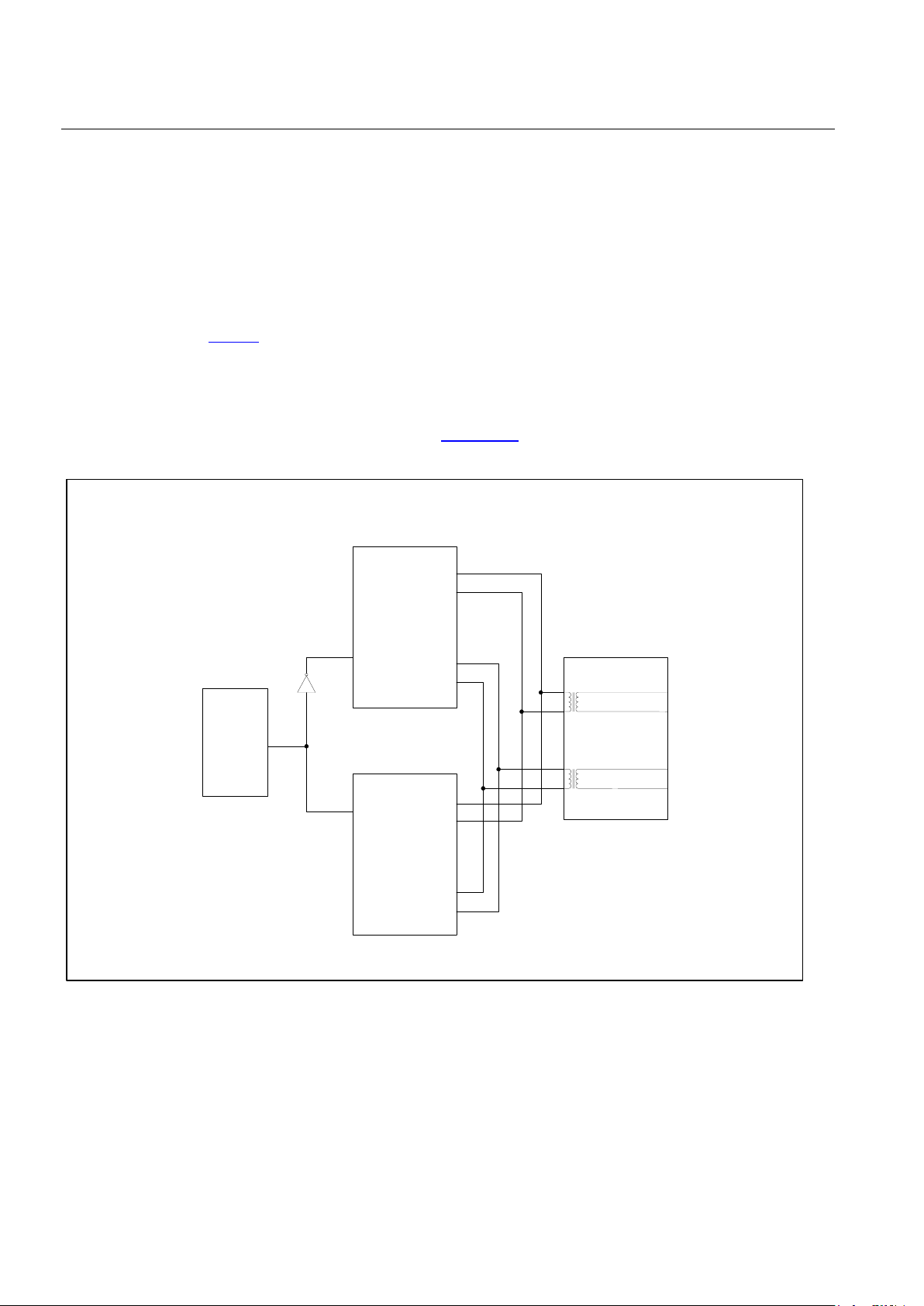
DS26518 8-Port T1/E1/J1 Transceiver
90 of 286
9.12.4 Hitless Protection Switching (HPS)
Many current redundancy protection implementations use mechanical relays to switch between primary and
backup boards. The switching time in relays is typically in the milliseconds, making T1/E1 HPS impossible. The
switching event will likely cause frame-synchronization loss in any equipment downstream, affecting the quality of
service. The same is also true for tri-stating mechanisms that use software or inactive clocks for the triggering of
HPS.
The DS26518 LIUs feature fast tristatable outputs for TTIPn and TRINGn and fast disabling of internal impedance
matching for RTIPn and RRINGn within one-bit period. The TXENABLE pin is used for hitless protection circuits in
combination with the
LTRCR.RHPM bit. When low, the TXENABLE pin tri-states all eight transmitters, providing a
high-impedance state on TTIPn and TRINGn. If the RHPM bit is set, the TXENABLE pin, when low, will also
disable the internal termination on RTIPn and RRINGn on a per-port basis, providing a high impedance to the
receive line.
This is a very useful function in that control can be done through a hardware pin, allowing a quick switch to the
backup system for both the receiver and the transmitter.
Figure 9-24 shows a typical HPS application.
Figure 9-24. HPS Block Diagram
PRIMARY
BOARD
BACKUP
BOARD
SWITCHING
CONTROL
TXENABLE
TRING
RTIP
TTIP
RRING
TRING
RTIP
TTIP
RRING
LINE
INTERFACE
CARD
RX
TX
TXENABLE
Page 91

DS26518 8-Port T1/E1/J1 Transceiver
91 of 286
9.12.5 Jitter Attenuator
The DS26518 contains a jitter attenuator that can be set to a depth of 32 or 128 bits via the JADS bits in LIU
Transmit and Receive Control Register (
LTRCR).
The 128-bit mode is used in applications where large excursions of wander are expected. The 32-bit mode is used
in delay sensitive applications. The characteristics of the attenuation are shown in
Figure 9-25. The jitter attenuator
can be placed in either the receive path or the transmit path, or be disabled by appropriately setting the JAPS1 and
JAPS0 bits in the LIU Transmit and Receive Control Register (
LTRCR).
For the jitter attenuator to operate properly, a 2.048MHz, 1.544MHz, or a multiple of up to 8x clock must be applied
at MCLK. See the Global Transceiver Clock Control Register 1 (
GTCCR1) for MCLK options. ITU-T specification
G.703 requires an accuracy of ±50ppm for both T1/J1 and E1 applications. TR62411 and ANSI specs require an
accuracy of ±32ppm for T1/J1 interfaces. Circuitry adjusts either the recovered clock from the clock/data recovery
block or the clock applied at the TCLKn pin to create a smooth jitter-free clock, which is used to clock data out of
the jitter attenuator FIFO. It is acceptable to provide a gapped/bursty clock at the TCLKn pin if the jitter attenuator is
placed in the transmit side. If the incoming jitter exceeds either 120UI
P-P
(buffer depth is 128-bits) or 28UI
P-P
(buffer
depth is 32 bits), then the DS26518 will set the jitter attenuator limit trip (JALTS) bit in the LIU Latched Status
Register (
LLSR.3). In T1/J1 mode, the jitter attenuator corner frequency is 3.75Hz, and in E1 mode it is 0.6Hz.
The DS26518 jitter attenuator is compliant with the following specifications shown in
Table 9-42.
Table 9-42. Jitter Attenuator Standards Compliance
Standard
ITU-T I.431, G.703, G.736, G.823
ETS 300 011, TBR 12/13
AT&T TR62411, TR43802
TR-TSY 009, TR-TSY 253, TR-TSY 499
Figure 9-25. Jitter Attenuation
FREQUENCY (Hz)
0dB
-20dB
-40dB
-60dB
1 10 100 1K 10K
JITTER ATTENUATION (dB)
100K
TR 62411 ( Dec . 90)
Prohibited Area
C
u
rv
e
B
C
urv
e
A
ITU G.7XX
Prohibited Area
TBR12
Prohibited
Area
T1E1
Page 92

DS26518 8-Port T1/E1/J1 Transceiver
92 of 286
9.12.6 LIU Loopbacks
The DS26518 provides four LIU loopbacks for diagnostic purposes: Analog Loopback, Local Loopback, Remote
Loopback 1, and Remote Loopback 2. Dual Loopback is a combination of Local Loopback and Remote Loopback
1. In the loopback diagrams that follow, TSERn, TCLKn, RSERn, and RCLKn are inputs/outputs from the framer.
Figure 9-26. Loopback Diagram
Jitter
Attenuator
(in RX path)
RSER
Jitter
Attenuator
(in TX path)
Local Loopback
Jitter
Attenuator
can be
assigned to
receive path
or transmit
path or
disabled
RTIP
RRING
TTIP
TRING
JACLK
Master Clock
PLL
MCLK
RCLK
Analog Loopback
Remote 2 Loopback
Remote 1 Loopback
TSER
TCLK
RX LIU
TX LIU TX FORMATTER
RX FRAMER
9.12.6.1 Analog Loopback
The analog output of the transmitter TTIPn and TRINGn is looped back to RTIPn and RRINGn of the receiver. Data
at RTIPn and RRINGn is ignored in analog loopback. This is shown in the
Figure 9-27.
Figure 9-27. Analog Loopback
Line
Driver
Transmit
Framer
Optional
Jitter
A
ttenuato
r
Transmit
Digital
Transmit
A
nalog
TCLK
Receive
Framer
Optional
Jitter
A
ttenuato
r
Receive
Digital
Receive
Analog
RCLK
RTIP
RRING
TSER
RSER
TTIP
TRING
Page 93
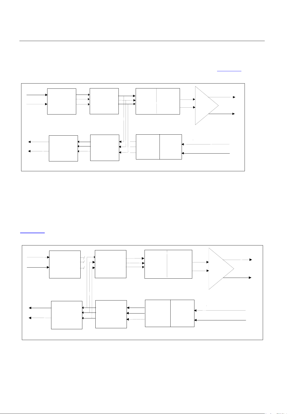
DS26518 8-Port T1/E1/J1 Transceiver
93 of 286
9.12.6.2 Local Loopback
The transmit system data is looped back to the receive framer. This data is also encoded and output on TTIPn and
TRINGn. Signals at RTIPn and RRINGn are ignored. This loopback is conceptually shown in
Figure 9-28.
Figure 9-28. Local Loopback
Line
Driver
Transmit
Framer
Optional
Jitter
A
ttenuator
Transmit
Digital
Transmit
A
nalog
TCLK
TSER
Receive
Framer
Optional
Jitter
A
ttenuator
Receive
Digital
Receive
A
nalog
RCLK
RSER
RTIP
RRING
TTIP
TRING
9.12.6.3 Remote Loopback 1
The outputs decoded from the receive LIU are looped back to the transmit LIU, not including the jitter attenuator in
the path. Remote Loopback 2 includes the jitter attenuator in the loopback path. The inputs from the transmit
framer are ignored during Remote Loopback 1.
9.12.6.4 Remote Loopback 2
The outputs decoded from the receive LIU are looped back to the transmit LIU, including the jitter attenuator. The
inputs from the transmit framer are ignored during Remote Loopback 2. This loopback is conceptually shown in
Figure 9-29.
Figure 9-29. Remote Loopback 2
Line
Driver
Transmit
Framer
Optional
Jitter
A
ttenuato
r
Transmit
Digital
Transmit
A
nalog
TCLK
TSER
Receive
Framer
Optional
Jitter
A
ttenuato
r
Receive
Digital
Receive
A
nalog
RCLK
RSER
RTIP
RRING
TTIP
TRING
Page 94
DS26518 8-Port T1/E1/J1 Transceiver
94 of 286
9.12.6.5 Dual Loopback
The inputs decoded from the receive LIU are looped back to the transmit LIU. The inputs from the transmit framer
are looped back to the receiver with the optional jitter attenuator. Dual Loopback is a combination of Local
Loopback and Remote Loopback 1. This loopback is invoked by setting the correct bits in the LIU Maintenance
Control Register (
LMCR). This loopback is conceptually shown in Figure 9-30.
Figure 9-30. Dual Loopback
Line
Driver
Transmit
Framer
Optional
Jitter
Attenuator
Transmit
Digital
Transmit
Analog
TCLK
TSER
Receive
Framer
Optional
Jitter
Attenuator
Receive
Digital
Receive
Analog
RCLK
RSER
RTIP
RRING
TTIP
TRING
Page 95

DS26518 8-Port T1/E1/J1 Transceiver
95 of 286
9.13 Bit Error-Rate Test Function (BERT)
The BERT (Bit Error Rate Tester) block can generate and detect both pseudorandom and repeating bit patterns. It
is used to test and stress data-communication links. BERT functionality is dedicated for each of the transceivers.
The registers related to the configure, control, and status of the BERT are shown in
Table 9-43.
Table 9-43. Registers Related to Configure, Control, and Status of BERT
REGISTER
FRAMER 1
ADDRESSES
FUNCTION
Global BERT Interrupt Status
Register 1 (
GBISR1)
00FAh
When any of the 8 BERTs issue an interrupt, a bit
will be set.
Global BERT Interrupt Mask Register
1 (
GBIMR1)
00FDh
When any of the 8 BERTs issue an interrupt, a bit
will be set.
Receive Expansion Port Control
Register (
RXPC)
08Ah Enable for the receiver BERT.
Receive BERT Port Bit Suppress
Register (
RBPBS)
08Bh Bit suppression for the receive BERT.
Receive BERT Port Channel Select
Registers 1 to 4 (
RBPCS1-4)
0D4h, 0D5h, 0D6h,
0D7h
Channels to be enabled for the Framer to accept
data from the BERT pattern generator
Transmit Expansion Port Control
Register (
TXPC)
18Ah Enable for the transmitter BERT.
Transmit BERT Port Bit Suppress
Register (
TBPBS)
18Bh Bit suppression for the transmit BERT.
Transmit BERT Port Channel Select
Registers 1 to 4 (
TBPCS1-4)
1D4h, 1D5h, 1D6h,
1D7h
Channels to be enabled for the framer to accept
data from the transmit BERT pattern generator.
BERT Alternating Word Count Rate
Register (
BAWC)
1100h BERT alternating pattern count register.
BERT Repetitive Pattern Set Register
1 (
BRP1)
1101h BERT repetitive pattern set register 1.
BERT Repetitive Pattern Set Register
2 (
BRP2)
1102h BERT repetitive pattern set register 2.
BERT Repetitive Pattern Set Register
3 (
BRP3)
1103h BERT repetitive pattern set register 3.
BERT Repetitive Pattern Set Register
4 (
BRP4)
1104h BERT repetitive pattern set register 4.
BERT Control Register 1 (BC1) 1105h Pattern selection and misc control
BERT Control Register 2 (BC2) 1106h BERT bit pattern length control
BERT Bit Count Register 1 (BBC1) 1107h Increments for BERT bit clocks.
BERT Bit Count Register 2 (BBC2) 1108h BERT bit counter.
BERT Bit Count Register 3 (BBC3) 1109h BERT bit counter.
BERT Bit Count Register 4 (BBC4) 110Ah BERT bit counter.
BERT Error Count Register 1 (BEC1) 110Bh BERT error counter.
BERT Error Count Register 2 (BEC2) 110Ch BERT error counter.
BERT Error Count Register 3 (BEC3) 110Dh BERT error counter.
BERT Latched Status Register
(
BLSR)
110Eh Denotes synchronization loss and other status.
BERT Status Interrupt Mask Register
(
BSIM)
110Fh BERT interrupt mask.
Note: The addresses shown above are for Framer 1. Addresses for Framers 2 to 8 can be calculated using the following: Framer N = (Framer 1
address + (n - 1) x 200hex); where n = 2 to 8 for Framers 2 to 8.
Page 96

DS26518 8-Port T1/E1/J1 Transceiver
96 of 286
The BERT block can generate and detect the following patterns:
• The pseudorandom patterns 2E7-1, 2E9-1, 2E11-1, 2E15-1, and QRSS.
• A repetitive pattern from 1 to 32 bits in length.
• Alternating (16-bit) words that flip every 1 to 256 words.
• Daly pattern.
The BERT function must be enabled and configured in the
TXPC and RXPC registers for each port. The BERT can
then be assigned on a per-channel basis for both the transmitter and receiver, using the special per-channel
function in the
TBPCS1-4 and RBCS1-4 registers. Individual bit positions within the channels can be suppressed
with the
TBPBS and RBPBS registers. Using combinations of these functions, the BERT pattern can be transmitted
and/or received in single or across multiple DS0s, contiguous or broken. Transmit and receive bandwidth
assignments are independent of each other.
The BERT receiver has a 32-bit bit counter and a 24-bit error counter. The BERT receiver can generate interrupts
on: a change in receive-synchronizer status, receive all zeros, receive all ones, error counter overflow, bit counter
overflow, and bit error detection. Interrupts from each of these events can be masked within the BERT function via
the BERT Status Interrupt Mask Register (
BSIM). If the software detects that the BERT has reported an event, then
the software must read the BERT Latched Status Register (
BLSR) to determine which event(s) has occurred.
9.13.1 BERT Repetitive Pattern Set
These registers must be properly loaded for the BERT to generate and synchronize to a repetitive pattern, a
pseudorandom pattern, alternating word pattern, or a Daly pattern. For a repetitive pattern that is fewer than 32
bits, the pattern should be repeated so that all 32 bits are used to describe the pattern. For example, if the pattern
was the repeating 5-bit pattern …01101… (where the rightmost bit is the one sent first and received first), then
BRP1 should be loaded with ADh, BRP2 with B5h, BRP3 with D6h, and BRP4 should be loaded with 5Ah. For a
pseudo-random pattern, all four registers should be loaded with all ones (i.e., FFh). For an alternating word pattern,
one word should be placed into BRP1 and BRP2 and the other word should be placed into BRP3 and BRP4. For
example, if the DDS stress pattern “7E” is to be described, the user would place 00h in BRP1, 00h in BRP2, 7Eh in
BRP3, and 7Eh in BRP4, and the alternating word counter would be set to 50 (decimal) to allow 100 bytes of 00h
followed by 100 bytes of 7Eh to be sent and received.
9.13.2 BERT Error Counter
Once BERT has achieved synchronization, this 24-bit counter will increment for each data bit received in error.
Toggling the LC control bit in BC1 can clear this counter. This counter saturates when full and will set the BECO
status bit in the
BLSR register.
Page 97

DS26518 8-Port T1/E1/J1 Transceiver
97 of 286
10. DEVICE REGISTERS
Thirteen address bits are used to control the settings of the registers. The registers control functions of the framers,
LIUs, and BERTs within the DS26518. The map is divided into eight framers, followed by eight LIUs and eight
BERTs. Global registers (applicable to all eight transceivers and BERTs) are located within the address space of
Framer 1.
The register details are provided in the following tables. The framer registers bits are provided for Framer 1 and
address bits A[12:8] determine the framer addressed.
10.1 Register Listings
The framer registers have an offset of 200 hex, the LIU registers have an offset of 20 hex, and the BERT registers
have an offset of 10 hex for each transceiver.
Table 10-1. Register Address Ranges (in Hex)
CHANNEL GLOBAL
RECEIVE
FRAMER
TRANSMIT
FRAMER
LIU BERT
— 00F0–00FF — — — —
CH1 — 0000–00EF 0100–01EF 1000–101F 1100–110F
CH2 — 0200–02EF 0300–03EF 1020–103F 1110–111F
CH3 — 0400–04EF 0500–05EF 1040–105F 1120–112F
CH4 — 0600–06EF 0700–07EF 1060–107F 1130–113F
CH5 — 0800–08EF 0900–09EF 1080–109F 1140–114F
CH6 — 0A00–0AEF 0B00–0BEF 10A0–10BF 1150–115F
CH7 — 0C00–0CEF 0D00–0DEF 10C0–10DF 1160–116F
CH8 — 0E00–0EEF 0F00–0FEF 10E0–10FF 1170–117F
Page 98

DS26518 8-Port T1/E1/J1 Transceiver
98 of 286
10.1.1 Global Register List
Table 10-2. Global Register List
GLOBAL REGISTER LIST
ADDRESS NAME DESCRIPTION R/W
00F0h GTCR1 Global Transceiver Control Register 1 R/W
00F1h GFCR1 Global Framer Control Register 1 R/W
00F2h GTCR3 Global Transceiver Control Register 3 R/W
00F3h GTCCR1 Global Transceiver Clock Control Register 1 R/W
00F4h GTCCR3 Global Transceiver Clock Control Register 3 R/W
00F5h — Reserved —
00F6h GSRR1 Global LIU Software Reset Register 1 R/W
00F7h — Reserved —
00F8h IDR Device Identification Register R
00F9h GFISR1 Global Framer Interrupt Status Register 1 R
00FAh GBISR1 Global BERT Interrupt Status Register 1 R
00FBh GLISR1 Global LIU Interrupt Status Register 1 R
00FCh GFIMR1 Global Framers Interrupt Mask Register 1 RW
00FDh GBIMR1 Global BERT Interrupt Mask Register 1 RW
00FEh GLIMR1 Global LIU Interrupt Mask Register 1 RW
Note 1: Reserved registers should only be written with all zeros.
Note 2:
The global registers are located in the framer address space. The corresponding address space for the other seven framers is
“Reserved,” and should be initialized with all zeros for proper operation.
Page 99

DS26518 8-Port T1/E1/J1 Transceiver
99 of 286
10.1.2 Framer Register List
Table 10-3. Framer Register List
Note that only Framer 1 address is presented here. The same set of registers definitions applies for transceivers 2 to 8 in accordance with the
DS26518 map offsets. Transceiver offset is [(n - 1) x 200 hex], where n designates the transceiver in question.
FRAMER REGISTER LIST
ADDRESS NAME DESCRIPTION R/W
000h E1RDMWE1 E1 Receive Digital Milliwatt Enable Register 1 R/W
001h E1RDMWE2 E1 Receive Digital Milliwatt Enable Register 2 R/W
002h E1RDMWE3 E1 Receive Digital Milliwatt Enable Register 3 R/W
003h E1RDMWE4 E1 Receive Digital Milliwatt Enable Register 4 R/W
004h–00Fh — Reserved —
010h RHC Receive HDLC Control Register R/W
011h RHBSE Receive HDLC Bit Suppress Register R/W
012h RDS0SEL Receive Channel Monitor Select Register R/W
013h RSIGC Receive-Signaling Control Register R/W
T1RCR2 Receive Control Register 2 (T1 Mode)
014h
E1RSAIMR Receive Sa-Bit Interrupt Mask Register (E1 Mode)
R/W
015h T1RBOCC Receive BOC Control Register (T1 Mode Only) R/W
016h–01Fh — Reserved —
020h RIDR1 Receive Idle Code Definition Register 1 R/W
021h RIDR2 Receive Idle Code Definition Register 2 R/W
022h RIDR3 Receive Idle Code Definition Register 3 R/W
023h RIDR4 Receive Idle Code Definition Register 4 R/W
024h RIDR5 Receive Idle Code Definition Register 5 R/W
025h RIDR6 Receive Idle Code Definition Register 6 R/W
026h RIDR7 Receive Idle Code Definition Register 7 R/W
027h RIDR8 Receive Idle Code Definition Register 8 R/W
028h RIDR9 Receive Idle Code Definition Register 9 R/W
029h RIDR10 Receive Idle Code Definition Register 10 R/W
02Ah RIDR11 Receive Idle Code Definition Register 11 R/W
02Bh RIDR12 Receive Idle Code Definition Register 12 R/W
02Ch RIDR13 Receive Idle Code Definition Register 13 R/W
02Dh RIDR14 Receive Idle Code Definition Register 14 R/W
02Eh RIDR15 Receive Idle Code Definition Register 15 R/W
02Fh RIDR16 Receive Idle Code Definition Register 16 R/W
030h RIDR17 Receive Idle Code Definition Register 17 R/W
031h RIDR18 Receive Idle Code Definition Register 18 R/W
032h RIDR19 Receive Idle Code Definition Register 19 R/W
033h RIDR20 Receive Idle Code Definition Register 20 R/W
034h RIDR21 Receive Idle Code Definition Register 21 R/W
035h RIDR22 Receive Idle Code Definition Register 22 R/W
036h RIDR23 Receive Idle Code Definition Register 23 R/W
037h RIDR24 Receive Idle Code Definition Register 24 R/W
T1RSAOI1 Receive-Signaling All-Ones Insertion Register 1 (T1 Mode Only)
038h
RIDR25 Receive Idle Code Definition Register 25 (E1 Mode)
R/W
T1RSAOI2 Receive-Signaling All-Ones Insertion Register 2 (T1 Mode Only)
039h
RIDR26 Receive Idle Code Definition Register 26 (E1 Mode)
R/W
T1RSAOI3 Receive-Signaling All-Ones Insertion Register 3 (T1 Mode Only)
03Ah
RIDR27 Receive Idle Code Definition Register 27 (E1 Mode)
R/W
03B RIDR28 Receive Idle Code Definition Register 28 (E1 Mode) —
T1RDMWE1 T1 Receive Digital Milliwatt Enable Register 1 (T1 Mode Only)
03C
RIDR29 Receive Idle Code Definition Register 29 (E1 Mode)
R/W
03Dh
T1RDMWE2 T1 Receive Digital Milliwatt Enable Register 2 (T1 Mode Only)
R/W
Page 100

DS26518 8-Port T1/E1/J1 Transceiver
100 of 286
FRAMER REGISTER LIST
ADDRESS NAME DESCRIPTION R/W
RIDR30 Receive Idle Code Definition Register 30 (E1 Mode)
T1RDMWE3 T1 Receive Digital Milliwatt Enable Register 3 (T1 Mode Only)
03Eh
RIDR31 Receive Idle Code Definition Register 31 (E1 Mode)
R/W
03Fh RIDR32 Receive Idle Code Definition Register 32 (E1 Mode) —
040h RS1 Receive-Signaling Register 1 R
041h RS2 Receive-Signaling Register 2 R
042h RS3 Receive-Signaling Register 3 R
043h RS4 Receive-Signaling Register 4 R
044h RS5 Receive-Signaling Register 5 R
045h RS6 Receive-Signaling Register 6 R
046h RS7 Receive-Signaling Register 7 R
047h RS8 Receive-Signaling Register 8 R
048h RS9 Receive-Signaling Register 9 R
049h RS10 Receive-Signaling Register 10 R
04Ah RS11 Receive-Signaling Registe r 11 R
04Bh RS12 Receive-Signaling Registe r 12 R
04Ch RS13 Receive-Signaling Register 13 (E1 Mode only) —
04Dh RS14 Receive-Signaling Register 14 (E1 Mode only) —
04Eh RS15 Receive-Signaling Register 15 (E1 Mode only) —
04Fh RS16 Receive-Signaling Register 16 (E1 Mode only) —
050h LCVCR1 Line Code Violation Count Register 1 R
051h LCVCR2 Line Code Violation Count Register 2 R
052h PCVCR1 Path Code Violation Count Register 1 R
053h PCVCR2 Path Code Violation Count Register 2 R
054h FOSCR1 Frames Out of Sync Count Register 1 R
055h FOSCR2 Frames Out of Sync Count Register 2 R
056h E1EBCR1 E-Bit Count 1 (E1 Mode Only) R
057h E1EBCR2 E-Bit Count 2 (E1 Mode Only) R
058h FEACR1 Error Count A Register 1 R/W
059h FEACR2 Error Count A Register 2 R/W
05Ah FEBCR1 Error Count B Register 1 R/W
05Bh FEBCR2 Error Count B Register 2 R/W
060h RDS0M Receive DS0 Monitor Register R
061h — Reserved —
T1RFDL Receive FDL Register (T1 Mode)
062h
E1RRTS7 Receive Real-Time Status Register 7 (E1 Mode)
R
063h T1RBOC Receive BOC Register (T1 Mode) R
T1RSLC1 Receive SLC-96 Data Link Register 1 (T1 Mode)
064h
E1RAF E1 Receive Align Frame Register (E1 Mode)
R
T1RSLC2 Receive SLC-96 Data Link Register 2 (T1 Mode)
065h
E1RNAF E1 Receive Non-Align Frame Register (E1 Mode)
R
T1RSLC3 Receive SLC-96 Data Link Register 3 (T1 Mode)
066h
E1RsiAF E1 Received Si Bits of the Align Frame Register (E1 Mode)
R
067h E1RSiNAF Received Si Bits of the Non-Align Frame Register (E1 Mode) R
068h E1RRA Received Remote Alarm Register (E1 Mode) R
069h E1RSa4 E1 Receive Sa4 Bits Register (E1 Mode Only) R
06Ah E1RSa5 E1 Receive Sa5 Bits Register (E1 Mode Only) R
06Bh E1RSa6 E1 Receive Sa6 Bits Register (E1 Mode Only) R
06Ch E1RSa7 E1 Receive Sa7 Bits Register (E1 Mode Only) R
06Dh E1RSa8 Receive Sa8 Bits Register (E1 Mode Only) R
06Eh SaBITS E1 Receive SaX Bits Register R
06Fh Sa6CODE Received Sa6 Codeword Regi ster R
070h–07Fh — Reserved —
 Loading...