

Page 1
November 8, 2007
DS25CP104
3.125 Gbps 4x4 LVDS Crosspoint Switch with Transmit
Pre-Emphasis and Receive Equalization
General Description
The DS25CP104 is a 3.125 Gbps 4x4 LVDS crosspoint switch
optimized for high-speed signal routing and switching over
lossy FR-4 printed circuit board backplanes and balanced cables. Fully differential signal paths ensure exceptional signal
integrity and noise immunity. The non-blocking architecture
allows connections of any input to any output or outputs. The
switch configuration can be accomplished via external pins or
the System Management Bus (SMBus) interface.
The DS25CP104 features four levels (Off, Low, Medium,
High) of transmit pre-emphasis (PE) and four levels (Off, Low,
Medium, High) of receive equalization (EQ) settable via the
SMBus interface. Off and Medium PE levels and Off and Low
EQ levels are settable with the external pins. In addition, the
SMBus circuitry enables the loss of signal (LOS
) monitors that
can inform a system of the presence of an open inputs condition (e.g. disconnected cable).
Wide input common mode range allows the switch to accept
signals with LVDS, CML and LVPECL levels; the output levels
are LVDS. A very small package footprint requires a minimal
space on the board while the flow-through pinout allows easy
board layout. Each differential input and output is internally
terminated with a 100Ω resistor to lower device insertion and
return losses, reduce component count and further minimize
board space.
Features
■
DC - 3.125 Gbps low jitter, low skew, low power operation
■
Pin and SMBus configurable, fully differential, nonblocking architecture
■
Pin (two levels) and SMBus (four levels) selectable preemphasis and equalization eliminate ISI jitter
■
Wide Input Common Mode Range enables easy interface
to CML and LVPECL drivers
■
LOS
circuitry detects open inputs fault condition
■
On-chip 100Ω input and output termination minimizes
insertion and return losses, reduces component count and
minimizes board space
■
8 kV ESD on LVDS I/O pins protects adjoining
components
■
Small 6 mm x 6 mm LLP-40 space saving package
Applications
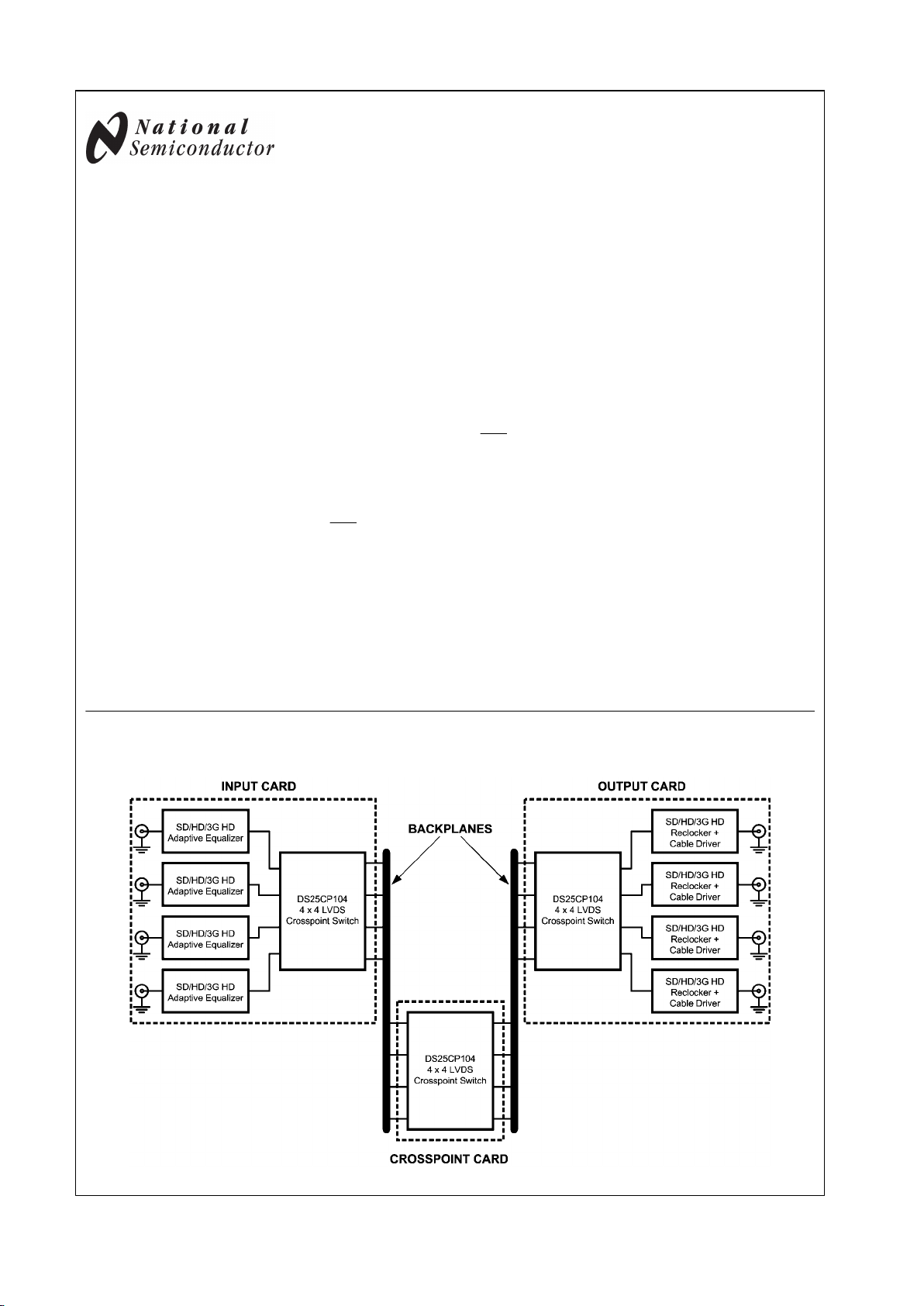
■
SD/HD/3G HD SDI Routers
■
OC-48 / STM-16
■
InfiniBand and FireWire
Typical Application
30003703
© 2007 National Semiconductor Corporation 300037 www.national.com
DS25CP104 3.125 Gbps 4x4 LVDS Crosspoint Switch with PE and EQ
Page 2
Ordering Code
NSID Function Available Equalization
Levels
Available Pre-Emphasis
Levels
DS25CP104TSQ Crosspoint Switch Off / Low / Medium / High Off / Low / Medium / High
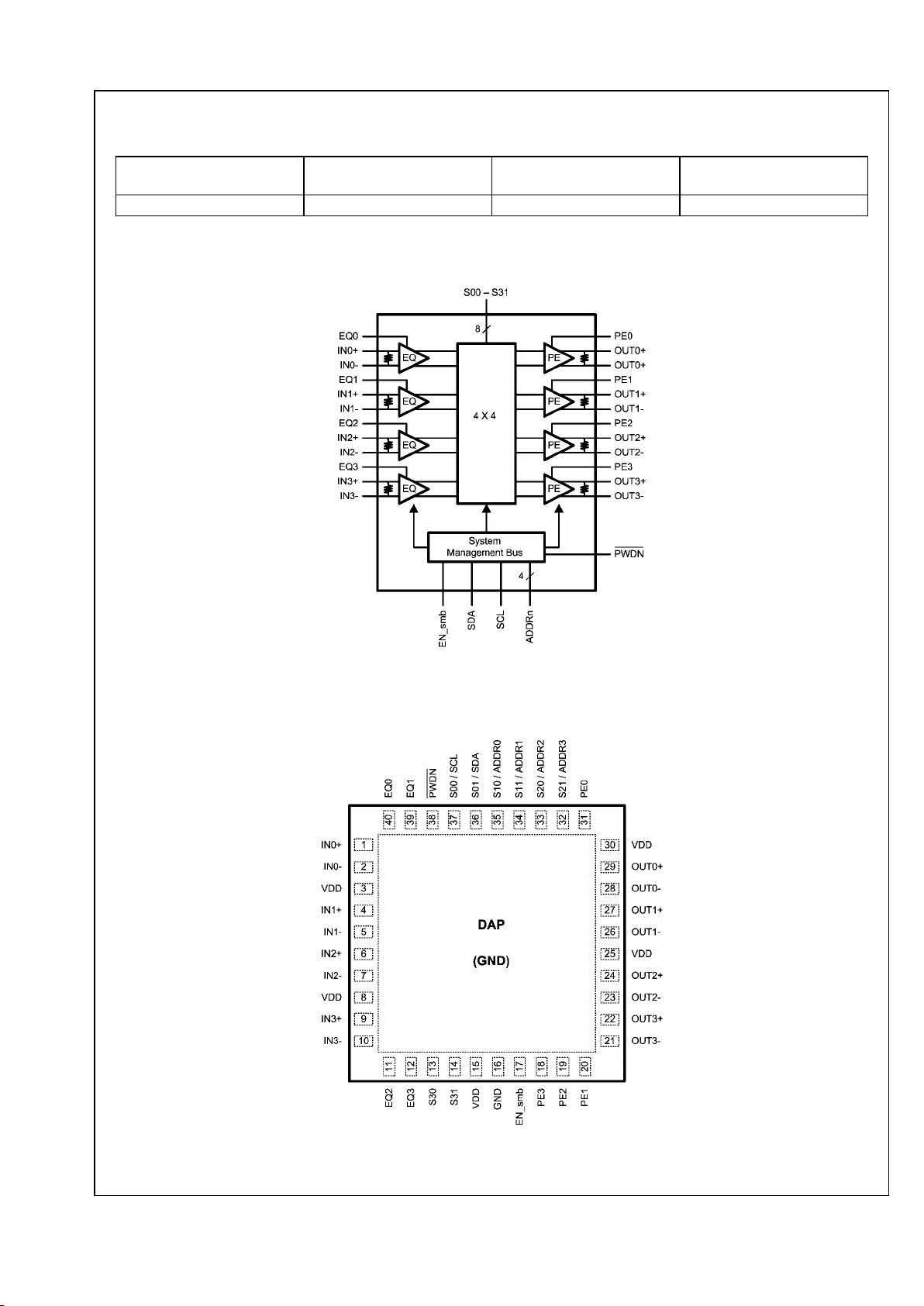
Block Diagram
30003701
Pin Diagram
30003702
DS25CP104 Pin Diagram
www.national.com 2
DS25CP104
Page 3
Pin Descriptions
Pin Name Pin
Number
I/O, Type Pin Description
IN0+, IN0- ,
IN1+, IN1-,
IN2+, IN2-,
IN3+, IN3-
1, 2,
4, 5,
6, 7,
9, 10
I, LVDS Inverting and non-inverting high speed LVDS input pins.
OUT0+, OUT0-,
OUT1+, OUT1-,
OUT2+, OUT2-,
OUT3+, OUT3-
29, 28,
27, 26,
24, 23,
22, 21
O, LVDS Inverting and non-inverting high speed LVDS output pins.
EQ0, EQ1,
EQ2, EQ3
40, 39,
11, 12
I, LVCMOS Receive equalization level select pins. These pins are functional
regardless of the EN_smb pin state.
PE0, PE1,
PE2, PE3
31, 20,
19, 18
I, LVCMOS Transmit pre-emphasis level select pins. These pins are functional
regardless of the EN_smb pin state.
EN_smb 17 I, LVCMOS System Management Bus (SMBus) enable pin. The pin has an
internal pull down. When the pin is set to a [1], the device is in the
SMBus mode. All SMBus registers are reset when this pin is
toggled. There is a 20k pulldown device on this pin.
S00/SCL 37 I, LVCMOS For EN_smb = [0], these pins select which LVDS input is routed
to the OUT0.
In the SMBus mode, when the EN_smb = [1], these pins are
SMBus clock input and data input pins respectively.
S01/SDA 36 I/O, LVCMOS
S10/ADDR0,
S11/ADDR1
35,
34
I, LVCMOS For EN_smb = [0], these pins select which LVDS input is routed
to the OUT1.
In the SMBus mode, when the EN_smb = [1], these pins are the
User-Set SMBus Slave Address inputs.
S20/ADDR2,
S21/ADDR3
33,
32
I, LVCMOS For EN_smb = [0], these pins select which LVDS input is routed
to the OUT2.
In the SMBus mode, when the EN_smb = H, these pins are the
User-Set SMBus Slave Address inputs.
S30, S31 13, 14 I, LVCMOS For EN_smb = [0], these pins select which LVDS input is routed
to the OUT3.
In the SMBus mode, when the EN_smb = [1], these pins are nonfunctional and should be tied to either logic H or L.
PWDN 38 I, LVCMOS For EN_smb = [0], this is the power down pin. When the PWDN is
set to a [0], the device is in the power down mode. The SMBus
circuitry can still be accessed provided the EN_smb pin is set to a
[1].
In the SMBus mode, the device is powered up by either setting the
PWDN pin to [1] OR by writing a [1] to the Control Register D[7]
bit ( SoftPWDN). The device will be powered down by setting the
PWDN pin to [0] AND by writing a [0] to the Control Register D[7]
bit ( SoftPWDN).
VDD 3, 8,
15,25, 30
Power Power supply pins.
GND 16, DAP Power Ground pin and a pad (DAP - die attach pad).
3 www.national.com
DS25CP104
Page 4
Absolute Maximum Ratings (Note 4)
If Military/Aerospace specified devices are required,
please contact the National Semiconductor Sales Office/
Distributors for availability and specifications.
Supply Voltage −0.3V to +4V
LVCMOS Input Voltage −0.3V to (VCC + 0.3V)
LVCMOS Output Voltage −0.3V to (VCC + 0.3V)
LVDS Input Voltage −0.3V to +4V
LVDS Differential Input Voltage 0V to 1.0V
LVDS Output Voltage −0.3V to (VCC + 0.3V)
LVDS Differential Output Voltage 0V to 1.0V
LVDS Output Short Circuit Current
Duration
5 ms
Junction Temperature +150°C
Storage Temperature Range −65°C to +150°C
Lead Temperature Range
Soldering (4 sec.) +260°C
Maximum Package Power Dissipation at 25°C
SQA Package 4.65W
Derate SQA Package 37.2 mW/°C above +25°C
Package Thermal Resistance
θ
JA
+26.9°C/W
θ
JC
+3.8°C/W
ESD Susceptibility
HBM (Note 1)
≥8 kV
MM (Note 2)
≥250V
CDM (Note 3)
≥1250V
Note 1: Human Body Model, applicable std. JESD22-A114C
Note 2: Machine Model, applicable std. JESD22-A115-A
Note 3: Field Induced Charge Device Model, applicable std.
JESD22-C101-C
Recommended Operating
Conditions
Min Typ Max Units
Supply Voltage (VCC) 3.0 3.3 3.6 V
Receiver Differential Input
Voltage (VID)
0 1 V
Operating Free Air
Temperature (TA)
−40 +25 +85 °C
SMBus (SDA, SCL) 3.6 V
DC Electrical Characteristics
Over recommended operating supply and temperature ranges unless otherwise specified. (Notes 5, 6, 7)
Symbol Parameter Conditions Min Typ Max Units
LVCMOS DC SPECIFICATIONS
V
IH
High Level Input Voltage 2.0 V
CC
V
V
IL
Low Level Input Voltage GND 0.8 V
I
IH
High Level Input Current VIN = 3.6V
VCC = 3.6V
0 ±10
μA
EN_smb pin 40 175 250
μA
I
IL
Low Level Input Current VIN = GND
VCC = 3.6V
0 ±10
μA
V
CL
Input Clamp Voltage ICL = −18 mA, VCC = 0V −0.9 −1.5 V
V
OL
Low Level Output Voltage IOL= 4 mA SDA pin 0.4 V
LVDS INPUT DC SPECIFICATIONS
V
ID
Input Differential Voltage 0 1 V
V
TH
Differential Input High Threshold
VCM = +0.05V or VCC-0.05V
0 +100 mV
V
TL
Differential Input Low Threshold
−100 0 mV
V
CMR
Input Common Mode Voltage Range
VID = 100 mV
0.05
VCC -
0.05
V
I
IN
Input Current
VIN = +3.6V or 0V
VCC = 3.6V or 0V
±1 ±10
μA
C
IN
Input Capacitance Any LVDS Input Pin to GND 1.7 pF
R
IN
Input Termination Resistor Between IN+ and IN-
100
Ω
www.national.com 4
DS25CP104
Page 5
Symbol Parameter Conditions Min Typ Max Units
LVDS OUTPUT DC SPECIFICATIONS
V
OD
Differential Output Voltage
RL = 100Ω
250 350 450 mV
ΔV
OD
Change in Magnitude of VOD for Complimentary
Output States
-35 35 mV
V
OS
Offset Voltage
RL = 100Ω
1.05 1.2 1.375 V
ΔV
OS
Change in Magnitude of VOS for Complimentary
Output States
-35 35 mV
I
OS
Output Short Circuit Current (Note 8)
OUT to GND -35 -55 mA
OUT to V
CC
7 55 mA
C
OUT
Output Capacitance Any LVDS Output Pin to GND
1.2 pF
R
OUT
Output Termination Resistor Between OUT+ and OUT-
100
Ω
SUPPLY CURRENT
I
CC1
Supply Current PWDN = 0 40 50 mA
I
CC2
Supply Current PWDN = 1
PE = Off, EQ = Off
Broadcast (1:4) Mode
145 175 mA
I
CC3
Supply Current PWDN = 1
PE = Off, EQ = Off
Quad Buffer (4:4) Mode
157 190 mA
Note 4: “Absolute Maximum Ratings” indicate limits beyond which damage to the device may occur, including inoperability and degradation of device reliability
and/or performance. Functional operation of the device and/or non-degradation at the Absolute Maximum Ratings or other conditions beyond those indicated in
the Recommended Operating Conditions is not implied. The Recommended Operating Conditions indicate conditions at which the device is functional and the
device should not be operated beyond such conditions.
Note 5: The Electrical Characteristics tables list guaranteed specifications under the listed Recommended Operating Conditions except as otherwise modified
or specified by the Electrical Characteristics Conditions and/or Notes. Typical specifications are estimations only and are not guaranteed.
Note 6: Current into device pins is defined as positive. Current out of device pins is defined as negative. All voltages are referenced to ground except VOD and
ΔVOD.
Note 7: Typical values represent most likely parametric norms for VCC = +3.3V and TA = +25°C, and at the Recommended Operation Conditions at the time of
product characterization and are not guaranteed.
Note 8: Output short circuit current (IOS) is specified as magnitude only, minus sign indicates direction only.
5 www.national.com
DS25CP104
Page 6
AC Electrical Characteristics
Over recommended operating supply and temperature ranges unless otherwise specified. (Notes 9, 10)
Symbol Parameter Conditions Min Typ Max Units
LVDS OUTPUT AC SPECIFICATIONS (Note 11)
t
PLHD
Differential Propagation Delay Low to
High
RL = 100Ω
480 650 ps
t
PHLD
Differential Propagation Delay High to
Low
460 650 ps
t
SKD1
Pulse Skew |t
PLHD
− t
PHLD
| , (Note 12) 20 100 ps
t
SKD2
Channel to Channel Skew , (Note 13) 40 125 ps
t
SKD3
Part to Part Skew , (Note 14) 50 200 ps
t
LHT
Rise Time
RL = 100Ω
80 150 ps
t
HLT
Fall Time 80 150 ps
t
ON
Power Up Time
Time from PWDN =LH to OUTn active
6 20
μs
t
OFF
Power Down Time
Time from PWDN =HL to OUTn inactive
8 25 ns
t
SEL
Select Time Time from Sn =LH or HL to new signal
at OUTn
8 12 ns
JITTER PERFORMANCE WITH EQ = Off, PE = Off (Note 11)(Figure 5)
t
RJ1
Random Jitter (RMS Value)
No Test Channels
(Note 15)
VID = 350 mV
VCM = 1.2V
Clock (RZ)
1.25 GHz 0.5 1.1 ps
t
RJ2
1.5625 GHz 0.5 1.1 ps
t
DJ1
Deterministic Jitter (Peak to Peak)
No Test Channels
(Note 16)
VID = 350 mV
VCM = 1.2V
K28.5 (NRZ)
2.5 Gbps 10 22 ps
t
DJ2
3.125 Gbps 10 27 ps
t
TJ1
Total Jitter (Peak to Peak)
No Test Channels
(Note 17)
VID = 350 mV
VCM = 1.2V
PRBS-23 (NRZ)
2.5 Gbps 0.07 0.11
UI
P-P
t
TJ2
3.125 Gbps 0.13 0.16
UI
P-P
www.national.com 6
DS25CP104
Page 7
Symbol Parameter Conditions Min Typ Max Units
JITTER PERFORMANCE WITH EQ = Off, PE = Low(Note 11) (Figure 6 Figure 9)
t
RJ1A
Random Jitter (RMS Value)
Test Channels A
(Note 15)
VID = 350 mV
VCM = 1.2V
Clock (RZ)
1.25 GHz 0.5 1.1 ps
t
RJ2A
1.5625 GHz 0.5 1.1 ps
t
DJ1A
Deterministic Jitter (Peak to Peak)
Test Channels A
(Note 16)
VID = 350 mV
VCM = 1.2V
K28.5 (NRZ)
2.5 Gbps 10 22 ps
t
DJ2A
3.125 Gbps 10 27 ps
JITTER PERFORMANCE WITH EQ = Off, PE = Medium (Note 11) (Figure 6 Figure 9)
t
RJ1B
Random Jitter (RMS Value)
Test Channels B
(Note 15)
VID = 350 mV
VCM = 1.2V
Clock (RZ)
1.25 GHz 0.5 1.1 ps
t
RJ2B
1.5625 GHz 0.5 1.1 ps
t
DJ1B
Deterministic Jitter (Peak to Peak)
Test Channels B
(Note 16)
VID = 350 mV
VCM = 1.2V
K28.5 (NRZ)
2.5 Gbps 12 30 ps
t
DJ2B
3.125 Gbps 12 30 ps
t
TJ1B
Total Jitter (Peak to Peak)
Test Channels B
(Note 17)
VID = 350 mV
VCM = 1.2V
PRBS-23 (NRZ)
2.5 Gbps 0.08 0.10
UI
P-P
t
TJ2B
3.125 Gbps 0.10 0.15
UI
P-P
JITTER PERFORMANCE WITH EQ = Off, PE = High (Note 11) (Figures 6, 9)
t
RJ1C
Random Jitter (RMS Value)
Test Channels C
(Note 15)
VID = 350 mV
VCM = 1.2V
Clock (RZ)
1.25 GHz 0.5 1.1 ps
t
RJ2C
1.5625 GHz 0.5 1.1 ps
t
DJ1C
Deterministic Jitter (Peak to Peak)
Test Channels C
(Note 16)
VID = 350 mV
VCM = 1.2V
K28.5 (NRZ)
2.5 Gbps 30 60 ps
t
DJ2C
3.125 Gbps 30 65 ps
7 www.national.com
DS25CP104
Page 8
Symbol Parameter Conditions Min Typ Max Units
JITTER PERFORMANCE WITH PE = Off, EQ = Low (Note 11) (Figure 7 Figure 9)
t
RJ1D
Random Jitter (RMS Value)
Test Channels D
(Note 15)
VID = 350 mV
VCM = 1.2V
Clock (RZ)
1.25 GHz 0.5 1.1 ps
t
RJ2D
1.5625 GHz 0.5 1.1 ps
t
DJ1D
Deterministic Jitter (Peak to Peak)
Test Channels D
(Note 16)
VID = 350 mV
VCM = 1.2V
K28.5 (NRZ)
2.5 Gbps 20 40 ps
t
DJ2D
3.125 Gbps 20 40 ps
t
TJ1D
Total Jitter (Peak to Peak)
Test Channels D
(Note 17)
VID = 350 mV
VCM = 1.2V
PRBS-23 (NRZ)
2.5 Gbps 0.08 0.15
UI
P-P
t
TJ2D
3.125 Gbps 0.09 0.20
UI
P-P
JITTER PERFORMANCE WITH PE = Off, EQ = Medium (Note 11) (Figures 7, 9)
t
RJ1E
Random Jitter (RMS Value)
Test Channels E
(Note 15)
VID = 350 mV
VCM = 1.2V
Clock (RZ)
1.25 GHz 0.5 1.1 ps
t
RJ2E
1.5625 GHz 0.5 1.1 ps
t
DJ1E
Residual Deterministic Jitter (Peak to
Peak)
Test Channels E
(Note 16)
VID = 350 mV
VCM = 1.2V
K28.5 (NRZ)
2.5 Gbps 35 60 ps
t
DJ2E
3.125 Gbps 28 55 ps
JITTER PERFORMANCE WITH PE = Off, EQ = High (Note 11) (Figures 7, 9)
t
RJ1F
Random Jitter (RMS Value)
Test Channels F
(Note 15)
VID = 350 mV
VCM = 1.2V
Clock (RZ)
1.25 GHz 1.3 1.8 ps
t
RJ2F
1.5625 GHz 1.4 2.4 ps
t
DJ1F
Residual Deterministic Jitter (Peak to
Peak)
Test Channels F
(Note 16)
VID = 350 mV
VCM = 1.2V
K28.5 (NRZ)
2.5 Gbps 30 75 ps
t
DJ2F
3.125 Gbps 35 90 ps
JITTER PERFORMANCE WITH PE = Medium, EQ = Low (Note 11) (Figures 7, 9)
t
RJ1G
Random Jitter (RMS Value)
Input Test Channels D
Output Test Channels B
(Note 15)
VID = 350 mV
VCM = 1.2V
Clock (RZ)
1.25 GHz 0.5 1.1 ps
t
RJ2G
1.5625 GHz 0.5 1.1 ps
t
DJ1G
Deterministic Jitter (Peak to Peak)
Input Test Channels D
Output Test Channels B
(Note 16)
VID = 350 mV
VCM = 1.2V
K28.5 (NRZ)
2.5 Gbps 25 ps
t
DJ2G
3.125 Gbps 20 ps
www.national.com 8
DS25CP104
Page 9
Symbol Parameter Conditions Min Typ Max Units
SMBus AC SPECIFICATIONS
f
SMB
SMBus Operating Frequency 10 100 kHz
t
BUF
Bus free time between Stop and Start
Conditions
4.7
μs
t
HD:SDA
Hold time after (Repeated) Start
Condition. After this period, the first clock
is generated.
4.0
μs
t
SU:SDA
Repeated Start Condition setup time. 4.7
μs
t
SU:SDO
Stop Condition setup time 4.0
μs
t
HD:DAT
Data hold time 300 ns
t
SU:DAT
Data setup time 250 ns
t
TIMEOUT
Detect clock low timeout 25 35 ms
t
LOW
Clock low period 4.7
μs
t
HIGH
Clock high period 4.0 50
μs
t
POR
Time in which a device must be
operational after power-on reset
500 ms
Note 9: The Electrical Characteristics tables list guaranteed specifications under the listed Recommended Operating Conditions except as otherwise modified
or specified by the Electrical Characteristics Conditions and/or Notes. Typical specifications are estimations only and are not guaranteed.
Note 10: Typical values represent most likely parametric norms for VCC = +3.3V and TA = +25°C, and at the Recommended Operation Conditions at the time of
product characterization and are not guaranteed.
Note 11: Specification is guaranteed by characterization and is not tested in production.
Note 12: t
SKD1
, |t
PLHD
− t
PHLD
|, Pulse Skew, is the magnitude difference in differential propagation delay time between the positive going edge and the negative
going edge of the same channel.
Note 13: t
SKD2
, Channel to Channel Skew, is the difference in propagation delay (t
PLHD
or t
PHLD
) among all output channels in Broadcast mode (any one input to
all outputs).
Note 14: t
SKD3
, Part to Part Skew, is defined as the difference between the same signal path of any two devices running at the same VCC and within 5°C of each
other within the operating temperature range.
Note 15: Measured on a clock edge with a histogram and an acummulation of 1500 histogram hits. Input stimulus jitter is subtracted geometrically.
Note 16: Tested with a combination of the 1100000101 (K28.5+ character) and 0011111010 (K28.5- character) patterns. Input stimulus jitter is subtracted
algebraically.
Note 17: Measured on an eye diagram with a histogram and an acummulation of 3500 histogram hits. Input stimulus jitter is subtracted.
9 www.national.com
DS25CP104
Page 10

DC Test Circuits
30003720
FIGURE 1. Differential Driver DC Test Circuit
AC Test Circuits and Timing Diagrams
30003721
FIGURE 2. Differential Driver AC Test Circuit
30003722
FIGURE 3. Propagation Delay Timing Diagram
30003723
FIGURE 4. LVDS Output Transition Times
www.national.com 10
DS25CP104
Page 11

Pre-Emphasis and Equalization Test Circuits
30003729
FIGURE 5. Jitter Performance Test Circuit
30003727
FIGURE 6. Pre-Emphasis Performance Test Circuit
30003726
FIGURE 7. Equalization Performance Test Circuit
11 www.national.com
DS25CP104
Page 12

30003730
FIGURE 8. Pre-Emphasis and Equalization Performance Test Circuit
30003728
FIGURE 9. Test Channel Block Diagram
Test Channel Loss Characteristics
The test channel was fabricated with Polyclad PCL-FR-370-Laminate/PCL-FRP-370 Prepreg materials (Dielectric constant of 3.7
and Loss Tangent of 0.02). The edge coupled differential striplines have the following geometries: Trace Width (W) = 5 mils, Gap
(S) = 5 mils, Height (B) = 16 mils.
Test Channel Length
(inches)
Insertion Loss (dB)
500 MHz 750 MHz 1000 MHz 1250 MHz 1500 MHz 1560 MHz
A 10 -1.2 -1.7 -2.0 -2.4 -2.7 -2.8
B 20 -2.6 -3.5 -4.1 -4.8 -5.5 -5.6
C 30 -4.3 -5.7 -7.0 -8.2 -9.4 -9.7
D 15 -1.6 -2.2 -2.7 -3.2 -3.7 -3.8
E 30 -3.4 -4.5 -5.6 -6.6 -7.7 -7.9
F 60 -7.8 -10.3 -12.4 -14.5 -16.6 -17.0
www.national.com 12
DS25CP104
Page 13

Functional Description
The DS25CP104 is a 3.125 Gbps 4x4 LVDS digital crosspoint
switch optimized for high-speed signal routing and switching
over lossy FR-4 printed circuit board backplanes and balanced cables. The DS25CP104 operates in two modes: Pin
Mode (EN_smb = 0) and SMBus Mode (EN_smb = 1).
When in the Pin Mode, the switch is fully configurable with
external pins. This is possible with two input select pins per
output (e.g. S00 and S01 pins for OUT0). There is also one
transmit pre-emphasis (PE) level select pin per output for
switching the PE levels between Medium and Off settings and
one receive equalization (EQ) level select pin per input for
switching the EQ levels between Low and Off settings.
In the Pin Mode, feedback from the LOS
(Loss Of Signal)
monitor circuitry is not available (there is not an LOS output
pin).
When in the SMBus Mode, the full switch configuration, four
levels of transmit pre-emphasis (Off, Low, Medium and High),
four levels of receive equalization (Off, Low, Medium and
High) and SoftPWDN can be programmed via the SMBus interface. In addition, by using the SMBus interface, a user can
obtain the feedback from the built-in LOS circuitry which detects an open inputs fault condition.
In the SMBus Mode, the S00 and S01 pins become SMBus
clock (SCL) input and data (SDA) input pins respectively; the
S10, S11, S21 and S21 pins become the User-Set SMBus
Slave Address input pins (ADDR0, 1, 2 and 3) while the S30
and S31 pins become non-functional (tieing these two pins to
either H or L is recommended if the device will function only
in the SMBus mode).
In the SMBus Mode, the PE and EQ select pins as well as the
PWDN pin remain functional. How these pins function in each
mode is explained in the following sections.
DS25CP104 OPERATION IN THE PIN MODE
Power Up
In the Pin Mode, when the power is applied to the device
power suppy pins, the DS25CP104 enters the Power Up
mode when the PWDN pin is set to logic H. When in the Power
Down mode (PWDN pin is set to logic L), all circuitry is shut
down except the minimum required circuitry for the LOS and
SMBus Slave operation.
Switch Configuration
In the Pin Mode, the DS25CP104 operates as a fully pin-configurable crosspoint switch. The following truth tables illustrate how the swich can be configured with external pins.
Switch Configuration Truth Tables
TABLE 1. Input Select Pins Configuration for the Output OUT0
S01 S00 INPUT SELECTED
0 0 IN0
0 1 IN1
1 0 IN2
1 1 IN3
TABLE 2. Input Select Pins Configuration for the Output OUT1
S11 S10 INPUT SELECTED
0 0 IN0
0 1 IN1
1 0 IN2
1 1 IN3
13 www.national.com
DS25CP104
Page 14

TABLE 3. Input Select Pins Configuration for the Output OUT2
S21 S20 INPUT SELECTED
0 0 IN0
0 1 IN1
1 0 IN2
1 1 IN3
TABLE 4. Input Select Pins Configuration for the Output OUT3
S31 S30 INPUT SELECTED
0 0 IN0
0 1 IN1
1 0 IN2
1 1 IN3
Setting Pre-Emphasis Levels
The DS25CP104 has one PE level select pin per output for
setting the transmit pre-emphasis to either Medium or Off level. The following is the transmit pre-emphasis truth table.
TABLE 5. Transmit Pre-Emphasis Truth Table
OUTPUT OUTn, n = {0, 1, 2, 3}
Pre-Emphasis Control Pin (PEn) State Pre-Emphasis Level
0 Off
1 Medium
Transmit Pre-emphasis Level Selection for an Output OUTn
Setting Equalization Levels
The DS25CP104 has one EQ level select pin per input for
setting the receive equalization to either Low or Off level. The
following is the receive equalization truth table.
TABLE 6. Receive Equalization Truth Table
INPUT INn, n = {0, 1, 2, 3}
Equalization Control Pin (EQn) State Equalization Level
0 Off
1 Low
Receive Equalization Level Selection for an Input INn
www.national.com 14
DS25CP104
Page 15

DS25CP104 OPERATION IN THE SMBUS MODE
The DS25CP104 operates as a slave on the System Management Bus (SMBus) when the EN_smb pin is set to a high
(1). Under these conditions, the SCL pin is a clock input while
the SDA pin is a serial data input pin.
Device Address
Based on the SMBus 2.0 specification, the DS25CP104 has
a 7-bit slave address. The three most significant bits of the
slave address are hard wired inside the DS25CP104 and are
“101”. The four least significant bits of the address are assigned to pins ADDR3-ADDR0 and are set by connecting
these pins to GND for a low (0) or to VCC for a high (1). The
complete slave address is shown in the following table:
TABLE 7. DS25CP104 Slave Address
1 0 1 ADDR3 ADDR2 ADDR1 ADDR0
MSB LSB
This slave address configuration allows up to sixteen
DS25CP104 devices on a single SMBus bus.
Transfer of Data via the SMBus
During normal operation the data on SDA must be stable during the time when SCK is high.
There are three unique states for the SMBus:
START: A HIGH to LOW transition on SDA while SCK is high
indicates a message START condition.
STOP: A LOW to HIGH transition on SDA while SCK is high
indicates a message STOP condition.
IDLE: If SCK and SDA are both high for a time exceeding
tBUF from the last detected STOP condition or if they are high
for a total exceeding the maximum specification for tHIGH
then the bus will transfer to the IDLE state.
SMBus Transactions
A transaction begins with the host placing the DS25CP104
SMBus into the START condition, then a byte (8 bits) is transferred, MSB first, followed by a ninth ACK bit. ACK bits are ‘0’
to signify an ACK, or ‘1’ to signify NACK, after this the host
holds the SCL line low, and waits for the receiver to raise the
SDA line as an ACKnowledge that the byte has been received.
Writing to a Register
To write a data value to a register in the DS25CP104, the host
writes three bytes to the DS25CP104. The first byte is the
device address—the device address is a 7 bit value, and if
writing to the DS25CP104 the last bit (LSB) is set to ‘0’ to
signify that the operation is a write. The second byte written
is the register address, and the third byte written is the data
to be written into the addressed register. If additional data
writes are performed, the register address is automatically incremented. At the end of the write cycle the host places the
bus in the STOP state.
Reading From a Register
To read the data value from a register, first the host writes the
device address with the LSB set to a ‘0’ denoting a write, then
the register address is written to the device. The host then
reasserts the START condition, and writes the device address
once again, but this time with the LSB set to a ‘1’ denoting a
read, and following this the DS25CP104 will drive the SDA
line with the data from the addressed register. The host indicates that it has finished reading the data by asserting a ‘1’
for the ACK bit. After reading the last byte, the host will assert
a ‘0’ for NACK to indicate to the DS25CP104 that it does not
require any more data.
15 www.national.com
DS25CP104
Page 16

Register Descriptions
There are five data registers in the DS25CP104 accessible via the SMBus interface.
TABLE 8. DS25CP104 SMBus Data Registers
Address
(hex)
Name Access Description
0 Switch Configuration R/W Switch Configuration Register
1 PE Level Select R/W Transmit Pre-emphasis Level Select Register
2 EQ Level Select R/W Receive Equalization Level Select Register
3 Control R/W Powerdown, LOS Enable and Pin Control Register
4 LOS RO Loss Of Signal (LOS) Reporting Register
30003710
FIGURE 10. DS25CP104 Registers Block Diagram
www.national.com 16
DS25CP104
Page 17

SWITCH CONFIGURATION REGISTER
The Switch Configuration register is utilized to configure the switch. The following two tables show the Switch Configuration Register
mapping and associated truth table.
Bit Default Bit Name Access Description
D[1:0] 00 Input Select 0 R/W Selects which input is routed to the OUT0.
D[3:2] 00 Input Select 1 R/W Selects which input is routed to the OUT1.
D[5:4] 00 Input Select 2 R/W Selects which input is routed to the OUT2.
D[7:6] 00 Input Select 3 R/W Selects which input is routed to the OUT3.
TABLE 9. Switch Configuration Register Truth Table
D1 D0 Input Routed to the OUT0
0 0 IN0
0 1 IN1
1 0 IN2
1 1 IN3
The truth tables for the OUT1, OUT2, and OUT3 outputs are identical to this table.
The switch configuration logic has a SmartPWDN circuitry which automatically optimizes the device's power consumption based
on the switch configuration (i.e. It places unused I/O blocks and other unused circuitry in the power down state).
PE LEVEL SELECT REGISTER
The PE Level Select register selects the pre-emphasis level for each of the outputs. The following two tables show the register
mapping and associated truth table.
Bit Default Bit Name Access Description
D[1:0] 00 PE Level Select 0 R/W Sets pre-emphasis level on the OUT0.
D[3:2] 00 PE Level Select 1 R/W Sets pre-emphasis level on the OUT1.
D[5:4] 00 PE Level Select 2 R/W Sets pre-emphasis level on the OUT2.
D[7:6] 00 PE Level Select 3 R/W Sets pre-emphasis level on the OUT3.
TABLE 10. PE Level Select Register Truth Table
D1 D0 Pre-Emphasis Level for the OUT0
0 0 Off
0 1 Low
1 0 Medium
1 1 High
NOTE: The truth tables for the OUT1, OUT2, and OUT3 outputs are identical to this table.
17 www.national.com
DS25CP104
Page 18

EQ LEVEL SELECT REGISTER
The EQ Level Select register selects the equalization level for each of the inputs. The following two tables show the register mapping
and associated truth table.
Bit Default Bit Name Access Description
D[1:0] 00 EQ Level Select 0 R/W Sets equalization level on the IN0.
D[3:2] 00 EQ Level Select 1 R/W Sets equalization level on the IN1.
D[5:4] 00 EQ Level Select 2 R/W Sets equalization level on the IN2.
D[7:6] 00 EQ Level Select 3 R/W Sets equalization level on the IN3.
TABLE 11. EQ Level Select Register Truth Table
D1 D0 Equalization Level for the IN0
0 0 Off
0 1 Low
1 0 Medium
1 1 High
NOTE: The truth tables for the IN1, IN2, and IN3 outputs are identical to this table.
CONTROL REGISTER
The Control register enables SoftPWDN control, individual output power down (PWDNn) control, LOS Circuitry Enable control, PE
Level Select Enable control and EQ Level Select Enable control via the SMBus. The following table shows the register mapping.
Bit Default Bit Name Access Description
D[3:0] 1111 PWDNn R/W Writing a [0] to the bit D[n] will power down the output OUTn
when either the PWDN pin OR the Control Register bit D[7]
(SoftPWDN) is set to a high [1].
D[4] 0 Ignore_External_EQ R/W Writing a [1] to the bit D[4] will ignore the state of the external
EQ pins and will allow setting the EQ levels via the SMBus
interface.
D[5] 0 Ignore_External_PE R/W Writing a [1] to the bit D[5] will ignore the state of the external
PE pins and will allow setting the PE levels via the SMBus
interface.
D[6] 0 EN_LOS R/W Writing a [1] to the bit D[6] will enable the LOS circuitry and
receivers on all four inputs. The SmartPWDN circuitry will not
disable any of the inputs nor any supporting LOS circuitry
depending on the switch configuration.
D[7] 0 SoftPWDN R/W Writing a [0] to the bit D[7] will place the device into the power
down mode. This pin is ORed together with the PWDN pin.
TABLE 12. DS25CP104 Power Modes Truth Table
PWDN SoftPWDN PWDNn DS25CP104 Power Mode
0 0 x Power Down Mode. In this mode, all circuitry is shut down except the
minimum required circuitry for the LOS and SMBus Slave operation. The
SMBus circuitry allows enabling the LOS circuitry and receivers on all inputs
in this mode by setting the EN_LOS bit to a [1].
0
1
1
1
0
1
x
x
x
Power Up Mode. In this mode, the SmartPWDN circuitry will automatically
power down any unused I/O and logic blocks and other supporting circuitry
depending on the switch configuration.
An output will be enabled only when the SmartPWDN circuitry indicates that
that particular output is needed for the particular switch configuration and
the respective PWDNn bit has logic high [1].
An input will be enabled when the SmartPWDN circuitry indicates that that
particular input is needed for the particular switch configuration or the
EN_LOS bit is set to a [1].
www.national.com 18
DS25CP104
Page 19

LOS REGISTER
The LOS
register reports an open inputs fault condition for each of the inputs. The following table shows the register mapping.
Bit Default Bit Name Access Description
D[0] 0 LOS0 RO Reading a [0] from the bit D[0] indicates an open inputs fault condition on
the IN0. A [1] indicates presence of a valid signal.
D[1] 0 LOS1 RO Reading a [0] from the bit D[1] indicates an open inputs fault condition on
the IN1. A [1] indicates presence of a valid signal.
D[2] 0 LOS2 RO Reading a [0] from the bit D[2] indicates an open inputs fault condition on
the IN2. A [1] indicates presence of a valid signal.
D[3] 0 LOS3 RO Reading a [0] from the bit D[3] indicates an open inputs fault condition on
the IN3. A [1] indicates presence of a valid signal.
D[7:4] 0000 Reserved RO Reserved for future use. Returns undefined value when read.
19 www.national.com
DS25CP104
Page 20

INPUT INTERFACING
The DS25CP104 accepts differential signals and allows simple AC or DC coupling. With a wide common mode range, the
DS25CP104 can be DC-coupled with all common differential drivers (i.e. LVPECL, LVDS, CML). The following three figures illustrate typical DC-coupled interface to common differential drivers. Note that the DS25CP104 inputs are internally terminated with
a 100Ω resistor.
30003731
Typical LVDS Driver DC-Coupled Interface to DS25CP104 Input
30003732
Typical CML Driver DC-Coupled Interface to DS25CP104 Input
30003733
Typical LVPECL Driver DC-Coupled Interface to DS25CP104 Input
www.national.com 20
DS25CP104
Page 21

OUTPUT INTERFACING
The DS25CP104 outputs signals that are compliant to the LVDS standard. Its outputs can be DC-coupled to most common differential receivers. The following figure illustrates typical DC-coupled interface to common differential receivers and assumes that
the receivers have high impedance inputs. While most differential receivers have a common mode input range that can accomodate
LVDS compliant signals, it is recommended to check respective receiver's data sheet prior to implementing the suggested interface
implementation.
30003734
Typical DS25CP104 Output DC-Coupled Interface to an LVDS, CML or LVPECL Receiver
21 www.national.com
DS25CP104
Page 22

Typical Performance
30003750
Total Jitter as a Function of Data Rate
30003751
Residual Jitter as a Function of Data Rate, FR4 Stripline
Length and EQ Level
30003752
Residual Jitter as a Function of Data Rate, FR4 Stripline
Length and EQ Level
30003753
Residual Jitter as a Function of Data Rate, FR4 Stripline
Length and EQ Level
www.national.com 22
DS25CP104
Page 23

30003754
Residual Jitter as a Function of Data Rate, FR4 Stripline
Length and PE Level
30003755
Residual Jitter as a Function of Data Rate, FR4 Stripline
Length and PE Level
30003756
Residual Jitter as a Function of Data Rate, FR4 Stripline
Length and PE Level
30003757
Supply Current as a Function of Data Rate and PE Level
23 www.national.com
DS25CP104
Page 24

30003762
A 2.5 Gbps NRZ PRBS-23 without PE
After 30" Differential FR-4 Stripline
H: 75 ps / DIV, V: 100 mV / DIV
30003760
A 2.5 Gbps NRZ PRBS-23 with High PE
After 2" Differential FR-4 Microstrip
H: 75 ps / DIV, V: 100 mV / DIV
30003764
A 2.5 Gbps NRZ PRBS-23 with High PE
After 30" Differential FR-4 Stripline
H: 75 ps / DIV, V: 100 mV / DIV
30003763
A 3.125 Gbps NRZ PRBS-23 without PE
After 30" Differential FR-4 Stripline
H: 50 ps / DIV, V: 100 mV / DIV
30003761
A 3.125 Gbps NRZ PRBS-23 with High PE
After 2" Differential FR-4 Microstrip
H: 50 ps / DIV, V: 100 mV / DIV
30003765
A 3.125 Gbps NRZ PRBS-23 with High PE
After 30" Differential FR-4 Stripline
H: 50 ps / DIV, V: 100 mV / DIV
www.national.com 24
DS25CP104
Page 25

30003766
A 2.5 Gbps NRZ PRBS-23 without EQ
After 60" Differential FR-4 Stripline
H: 75 ps / DIV, V: 100 mV / DIV
30003768
A 2.5 Gbps NRZ PRBS-23 with High EQ
After 60" Differential FR-4 Stripline
H: 75 ps / DIV, V: 100 mV / DIV
30003767
A 3.125 Gbps NRZ PRBS-23 without EQ
After 60" Differential FR-4 Stripline
H: 50 ps / DIV, V: 100 mV / DIV
30003769
A 3.125 Gbps NRZ PRBS-23 with High EQ
After 60" Differential FR-4 Stripline
H: 50 ps / DIV, V: 100 mV / DIV
25 www.national.com
DS25CP104
Page 26

Physical Dimensions inches (millimeters) unless otherwise noted
Order Number DS25CP104TSQ
NS Package Number SQA40A
(See AN-1187 for PCB Design and Assembly Recommendations)
www.national.com 26
DS25CP104
Page 27

Notes
27 www.national.com
DS25CP104
Page 28

Notes
DS25CP104 3.125 Gbps 4x4 LVDS Crosspoint Switch with PE and EQ
For more National Semiconductor product information and proven design tools, visit the following Web sites at:
Products Design Support
Amplifiers www.national.com/amplifiers WEBENCH www.national.com/webench
Audio www.national.com/audio Analog University www.national.com/AU
Clock Conditioners www.national.com/timing App Notes www.national.com/appnotes
Data Converters www.national.com/adc Distributors www.national.com/contacts
Displays www.national.com/displays Green Compliance www.national.com/quality/green
Ethernet www.national.com/ethernet Packaging www.national.com/packaging
Interface www.national.com/interface Quality and Reliability www.national.com/quality
LVDS www.national.com/lvds Reference Designs www.national.com/refdesigns
Power Management www.national.com/power Feedback www.national.com/feedback
Switching Regulators www.national.com/switchers
LDOs www.national.com/ldo
LED Lighting www.national.com/led
PowerWise www.national.com/powerwise
Serial Digital Interface (SDI) www.national.com/sdi
Temperature Sensors www.national.com/tempsensors
Wireless (PLL/VCO) www.national.com/wireless
THE CONTENTS OF THIS DOCUMENT ARE PROVIDED IN CONNECTION WITH NATIONAL SEMICONDUCTOR CORPORATION
(“NATIONAL”) PRODUCTS. NATIONAL MAKES NO REPRESENTATIONS OR WARRANTIES WITH RESPECT TO THE ACCURACY
OR COMPLETENESS OF THE CONTENTS OF THIS PUBLICATION AND RESERVES THE RIGHT TO MAKE CHANGES TO
SPECIFICATIONS AND PRODUCT DESCRIPTIONS AT ANY TIME WITHOUT NOTICE. NO LICENSE, WHETHER EXPRESS,
IMPLIED, ARISING BY ESTOPPEL OR OTHERWISE, TO ANY INTELLECTUAL PROPERTY RIGHTS IS GRANTED BY THIS
DOCUMENT.
TESTING AND OTHER QUALITY CONTROLS ARE USED TO THE EXTENT NATIONAL DEEMS NECESSARY TO SUPPORT
NATIONAL’S PRODUCT WARRANTY. EXCEPT WHERE MANDATED BY GOVERNMENT REQUIREMENTS, TESTING OF ALL
PARAMETERS OF EACH PRODUCT IS NOT NECESSARILY PERFORMED. NATIONAL ASSUMES NO LIABILITY FOR
APPLICATIONS ASSISTANCE OR BUYER PRODUCT DESIGN. BUYERS ARE RESPONSIBLE FOR THEIR PRODUCTS AND
APPLICATIONS USING NATIONAL COMPONENTS. PRIOR TO USING OR DISTRIBUTING ANY PRODUCTS THAT INCLUDE
NATIONAL COMPONENTS, BUYERS SHOULD PROVIDE ADEQUATE DESIGN, TESTING AND OPERATING SAFEGUARDS.
EXCEPT AS PROVIDED IN NATIONAL’S TERMS AND CONDITIONS OF SALE FOR SUCH PRODUCTS, NATIONAL ASSUMES NO
LIABILITY WHATSOEVER, AND NATIONAL DISCLAIMS ANY EXPRESS OR IMPLIED WARRANTY RELATING TO THE SALE
AND/OR USE OF NATIONAL PRODUCTS INCLUDING LIABILITY OR WARRANTIES RELATING TO FITNESS FOR A PARTICULAR
PURPOSE, MERCHANTABILITY, OR INFRINGEMENT OF ANY PATENT, COPYRIGHT OR OTHER INTELLECTUAL PROPERTY
RIGHT.
LIFE SUPPORT POLICY
NATIONAL’S PRODUCTS ARE NOT AUTHORIZED FOR USE AS CRITICAL COMPONENTS IN LIFE SUPPORT DEVICES OR
SYSTEMS WITHOUT THE EXPRESS PRIOR WRITTEN APPROVAL OF THE CHIEF EXECUTIVE OFFICER AND GENERAL
COUNSEL OF NATIONAL SEMICONDUCTOR CORPORATION. As used herein:
Life support devices or systems are devices which (a) are intended for surgical implant into the body, or (b) support or sustain life and
whose failure to perform when properly used in accordance with instructions for use provided in the labeling can be reasonably expected
to result in a significant injury to the user. A critical component is any component in a life support device or system whose failure to perform
can be reasonably expected to cause the failure of the life support device or system or to affect its safety or effectiveness.
National Semiconductor and the National Semiconductor logo are registered trademarks of National Semiconductor Corporation. All other
brand or product names may be trademarks or registered trademarks of their respective holders.
Copyright© 2007 National Semiconductor Corporation
For the most current product information visit us at www.national.com
National Semiconductor
Americas Customer
Support Center
Email:
new.feedback@nsc.com
Tel: 1-800-272-9959
National Semiconductor Europe
Customer Support Center
Fax: +49 (0) 180-530-85-86
Email: europe.support@nsc.com
Deutsch Tel: +49 (0) 69 9508 6208
English Tel: +49 (0) 870 24 0 2171
Français Tel: +33 (0) 1 41 91 8790
National Semiconductor Asia
Pacific Customer Support Center
Email: ap.support@nsc.com
National Semiconductor Japan
Customer Support Center
Fax: 81-3-5639-7507
Email: jpn.feedback@nsc.com
Tel: 81-3-5639-7560
www.national.com
 Loading...