

Page 1

www.dalsemi.com
1-Wire
DS2415
TM
Time Chip
FEATURES
Real Time Clock with fully compatible 1-
Wire MicroLAN interface
Uses the same binary time/date
representation as the DS2404 but with 1
second resolution
Clock accuracy ±2 minutes per month at
25°C
Communicates at 16.3 kbits per second
Unique, factory-lasered and tested 64-bit
registration number (8-bit family code + 48bit serial number + 8-bit CRC tester) assures
absolute traceability because no two parts are
alike
8-bit family code specifies device
communication requirements to bus master
Built-in multidrop controller ensures
compatibility with other MicroLAN products
Operates over a wide VDD voltage range of
2.5V to 5.5V from -40°C to +85°C
Low power, 200 nA typically with oscillator
running
Compact, low cost 6-pin TSOC surface
mount package
PIN ASSIGNMENT
6-Pin TSOC PACKAGE
TOP VIEW
PIN DESCRIPTION
Pin 1 - GND
Pin 2 - 1-Wire
Pin 3 - V
Pin 4 - V
Pin 5 - X1
Pin 6 - X2
DD
BAT
ORDERING INFORMATION
DS2415P 6-pin TSOC package
DS2415V Tape & Reel of DS2415P
DS2415X Chip Scale Pkg., Tape & Reel
DESCRIPTION
The DS2415 1-Wire Time Chip offers a simple solution for storing and retrievin g vital time information
with minimal hardware. The DS2415 contains a unique, lasered ROM and a real time clock/calendar
implemented as a binary counter. Only one pin is required for communication with the devi ce. Utiliz ing a
backup energy source, the data is nonvolatile and allows for st and-alone operation. Th e DS2415 features
can be used to add functions such as calendar, time and date stamp and logbook to any t ype of electronic
device or embedded application that uses a microcontroller.
OVERVIEW
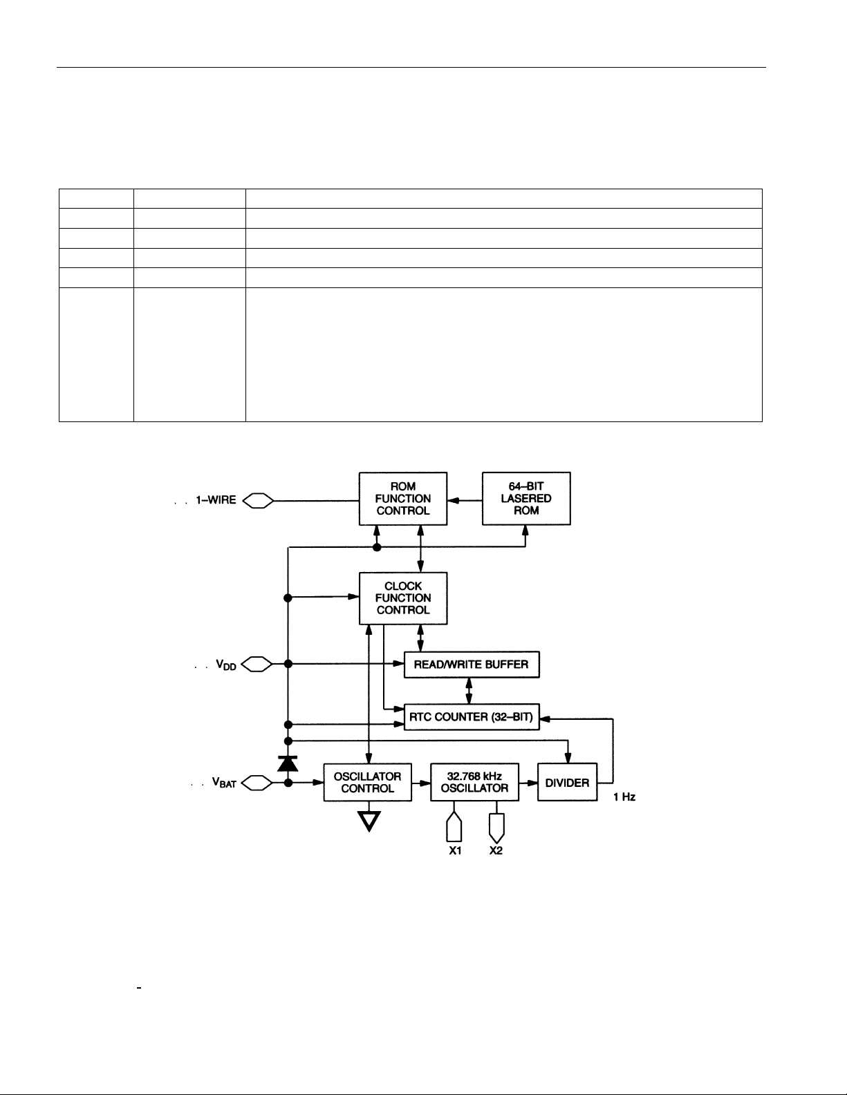
The DS2415 has two main data components: 1) 64-bit lasered ROM, and 2) real time clock counter
(Figure 1). The real time clock utilizes an on-chip oscillator that is connected to an external 32.768 kHz
crystal. All data is read and written least significant bit first. The real time clock functions will not be
available until the ROM function protocol has been established. This protocol is described in the ROM
1 of 14 013100
Page 2
DS2415
Functions flow chart (Figure 7). The master must first provide one of four ROM function commands: 1)
Read ROM, 2) Match ROM, 3) Search ROM, 4) Skip ROM. After a ROM function sequence has been
successfully executed, the real time clock functions are accessible and the master m a y then provide a re al
time clock function command (Figure 5).
DETAILED PIN DESCRIPTION
PIN SYMBOL DESCRIPTION
1 GND
21-WireData input/output. Open drain.
3VDDInternal power line. Connect a capacitor
4V
5,6 X1,X2
BAT
Ground pin.
Power input pin. 2.5V to 5.5V.
Crystal pins. Connections for a standard 32.768 kHz quartz crystal,
EPSON part number C-002RX or C-004R (be sure to request 6 pF load
capacitance).
NOTE: X1 and X2 are very high-impedance nodes. It is recommended
that they and the crystal be guard-ringed with ground and that high
frequency signals be kept away from the crystal area. See Figure 10 and
Application Note 58 for details.
BLOCK DIAGRAM Figure 1
64-BIT LASERED ROM
Each DS2415 contains a unique ROM code that is 64 bits long. The first 8 bits are a 1-Wire family code.
The next 48 bits are a unique serial number. The last 8 bits are a CRC of the first 56 bits. (See Figure 3.)
The 1-Wire CRC of the lasered ROM is generated using the polynomial X8 + X5 + X4 + 1. Additional
information about the Dallas Semiconductor 1-Wire Cyclic Redundancy Check is available in the Book
of DS19xx iButton Standards. The 64-bit ROM and ROM Function Control section allow the DS2415 to
operate as a 1-Wire device and follow the 1-Wire protocol detailed in the section ”1-Wire Bus S ystem.”
2 of 14
Page 3
DS2415
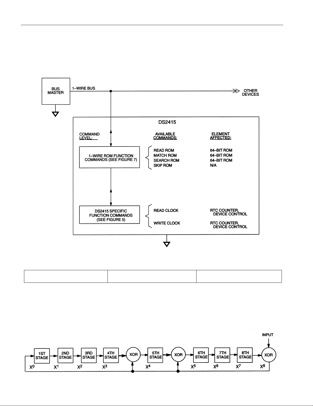
The functions required to exercise the control functions of the DS2415 are not accessible until the ROM
function protocol has been satisfied. This protocol is described in the ROM functions flow chart
(Figure 7). The 1-Wire bus master must first provide one of the four ROM function commands. After a
ROM function sequence has been successfully executed, the bus master may then provide one of the
function commands specific to the DS2415 (Figure 5).
HIERARCHICAL STRUCTURE FOR 1-WIRE PROTOCOL Figure 2
64-BIT LASERED ROM Figure 3
MSB LSB
8-Bit CRC Code 48-Bit Serial Number 8-Bit Family Code (24H)
MSB LSB MSB LSB MSB LSB
1-WIRE CRC GENERATOR Figure 4
Polynomial = X8 + X5 + X4 + 1
3 of 14
Page 4

DS2415
TIMEKEEPING
A 32.768 kHz crystal oscillator is used as the time base for the real time clock counter. The oscillator can
be turned on or off under software control. The oscillator must be on for the real time clock to function.
The real time clock counter is double-buffered. This allows the master to read time without the data
changing while it is being read. To accomplish this, a snapshot of the counter data is transferred to a
read/write buffer, which the user accesses.
DEVICE CONTROL BYTE
The on/off control of the 32.768 kHz crystal oscillator is done through the device control byte. This byte
can be read and written through the Clock Function commands.
Device Control Byte
76543210
U4 U3 U2 U1
Bit 0 - 1 0 No function
Bits 0 and 1 are hard-wired to read all 0s.
Bit 2 - 3 OSC Oscillator Enable/Disable
These bits control/report whether the 32.768 kHz crystal oscillator is running. If the oscillator is running,
both OSC bits will read 1. If the oscillator is turned off these bits will read 0. When writing the device
control byte both occurrences of the OSC bit should have identical data. Otherwise the value in bit
address 3 (bold) takes precedence.
Bit 4 - 7 Un General-purpose user flags
These bits have no particular function within the chip. They can be read and written under the control of
the application software and remain non-volatile as long as there is sufficient voltage at the VDD pin. If
the DS2415 is located inside a battery pack, for example, these bits could convey data on the charging
status from the charging station to the equipment that uses the battery.
OSC
OSC 0 0
Real time Clock
The real time clock is a 32-bit binary counter. It is incremented once per second. The real time clock can
accumulate 136 years of seconds before rolling over. Time/date is represented by the number of seconds
since a reference point, which is determined by the user. For example, 12:00 a.m., January 1, 1970 could
be a reference point.
CLOCK FUNCTION COMMANDS
The “Clock Function Flow Chart” (Figure 5) describes the protocols necessary for accessing the real time
clock. With only 4 bytes of real time clock and one control byte the DS2415 does not provide random
access. Reading and writing always starts with the device control byte followed by the least significant
byte of the time data.
4 of 14
Page 5

DS2415
READ CLOCK [66h]
The Read Clock command is used to read the device control byte and the contents of the real time clock
counter. After having received the most significant bit of the command code the device copies the actual
contents of the real time clock counter to the read/write buffer. Now the bus master re ads data beginning
with the device control byte followed by the least significant byte through the most significant byte of the
real time clock. After this the bus master may continue reading from the DS2415. The data received will
be the same as in the first pass through the command flow. The Read Clock command can be ended at
any point by issuing a Reset Pulse.
WRITE CLOCK [99h]
The Write Clock command is used to set the real time clock counter and to write the d evice control b yte.
After issuing the command, the bus master writes first the device control byte, which becomes
immediately effective. After this the bus master sends the least significant byte through the most
significant byte to be written to the real time clock counter. The new time data is copied from the
read/write buffer to the real time clock counter and becomes effective as the bus master generates a Reset
Pulse. If the oscillator is intentionally stopped the real time clock counter behaves as a 4-byte nonvolatile memory.
5 of 14
Page 6
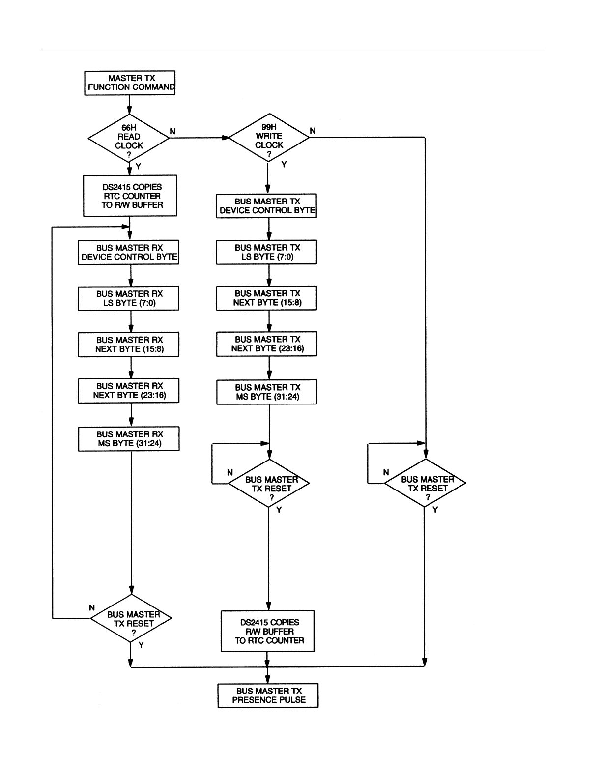
CLOCK FUNCTION COMMAND FLOW CHART Figure 5
DS2415
6 of 14
Page 7
DS2415
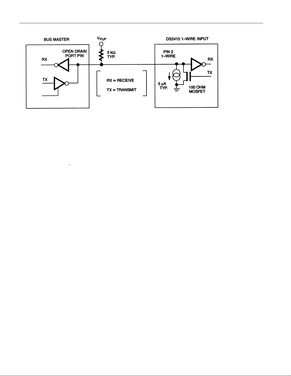
HARDWARE CONFIGURATION Figure 6
1-WIRE BUS SYSTEM
The 1-Wire bus is a system which has a single bus master and one or more slaves. In all instances the
DS2415 behaves as a slave. The discussion of this bus system is broken down into three topics: hard ware
configuration, transaction sequence, and 1-Wire signaling (signal types and timing). A 1-Wire protocol
defines bus transactions in terms of the bus state during specified time slots that are initiated on the falling
edge of sync pulses from the bus master. For a more detailed protocol description, refer to Chapter 4 of
the Book of DS19xx iButton Standards.
Hardware Configuration
The 1-Wire bus has only a single line by definition; it is import ant that each device on the bus be able t o
drive it at the appropriate time. To facilitate this, each device attached to the 1-Wire bus must have open
drain or 3-state outputs. The 1-Wire input of the DS2415 is open drain with an internal circuit equivalent
to that shown in Figure 6. A multidrop bus consists of a 1-Wire bus with multiple slaves attached. The 1Wire bus has a maximum data rate of 16.3k bits per second and requires a pullup resistor of
approximately 5 kΩ.
The idle state for the 1-Wire bus is high. If for any reason a transaction needs to be suspended, the bus
MUST be left in the idle state if the transaction is to resume. If this does not occur and the bus is left low
for more than 120 µs, one or more of the devices on the bus may be reset. Since the DS2415 gets all its
energy for operation through its V
for an extended time period.
pin it will NOT perform a power-on reset if the 1-Wire bus is low
BAT
Transaction Sequence
The protocol for accessing the DS2415 via the 1-Wire port is as follows:
Initialization
ROM Function Command
Clock Function Command
INITIALIZATION
All transactions on the 1-ire bus begin with an initialization sequence. The initialization sequence consists
of a Reset Pulse transmitted by the bus master followed by Presence Pulse(s) transmitted by the slave(s).
7 of 14
Page 8

DS2415
The Presence Pulse lets the bus master know that the DS2415 is on the bus and is ready to operate. For
more details, see the “1-Wire Signaling” section.
ROM FUNCTION COMM ANDS
Once the bus master has detected a presence, it can issue one of the four ROM function commands. All
ROM function commands are 8 bits long. A list of these commands follows (refer to flowchart in
Figure 7):
Read ROM [33h]
This command allows the bus master to read the DS2415s 8-bit family code, unique 48-bit serial number,
and 8-bit CRC. This command can only be used if there is a single DS2415 on the bus. If more than one
slave is present on the bus, a data collision will occur when all slaves try to transmit at the same time
(open drain will produce a wired-AND result). The resultant family code and 48-bit serial number will
usually result in a mismatch of the CRC.
Match ROM [55h]
The Match ROM command, followed by a 64-bit ROM sequence, allows the bus master to address a
specific DS2415 on a multidrop bus. Only the DS2415 that exactly matches the 64-bit ROM sequence
will respond to the following clock function command. All slaves that do not match the 64-bit ROM
sequence will wait for a Reset Pulse. This command can be used with a single or multiple devices on the
bus.
Skip ROM [CCh]
This command can save time in a single drop bus system by allowing the bus master to access the
memory functions without providing the 64-bit ROM code. If more than one slave is present on the bus
and a read command is issued following the Skip ROM command, data collision will occur on the bus as
multiple slaves transmit simultaneously (open drain pulldowns will produce a wired-AND result).
Search ROM [F0h]
When a system is initially brought up, the bus master might not know the number of devices on the 1Wire bus or their 64-bit ROM codes. The Search ROM command allows the bus master to use a process
of elimination to identify the 64-bit ROM codes of all slave devices on the bus. The Search ROM process
is the repetition of a simple, three-step routine: read a bit, read the complement of the bit, then write the
desired value of that bit. The bus master performs this simple, three-step routine on each bit of the ROM.
After one complete pass, the bus master knows the contents of the ROM in one device. The remaining
number of devices and their ROM codes may be identified by additional passes. See Chapter 5 of the
Book of DS19xx iButton Standards for a comprehensive discussion of a se arc h ROM, including an actu al
example.
8 of 14
Page 9
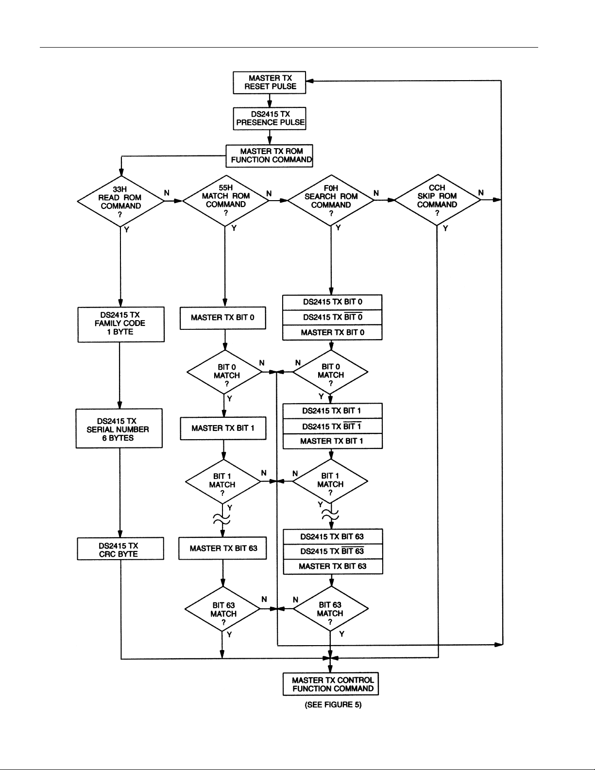
ROM FUNCTIONS FLOW CHART Figure 7
DS2415
9 of 14
Page 10
DS2415
1-WIRE SIGNALING
The DS2415 requires strict protocols to insure data integrity. The protocol consists of four types of
signaling on one line: Reset Sequence with Reset Pulse and Presence Pulse, Write 0, Write 1 and Read
Data. All these signals except Presence Pulse are initiated by the bus master. The initialization sequence
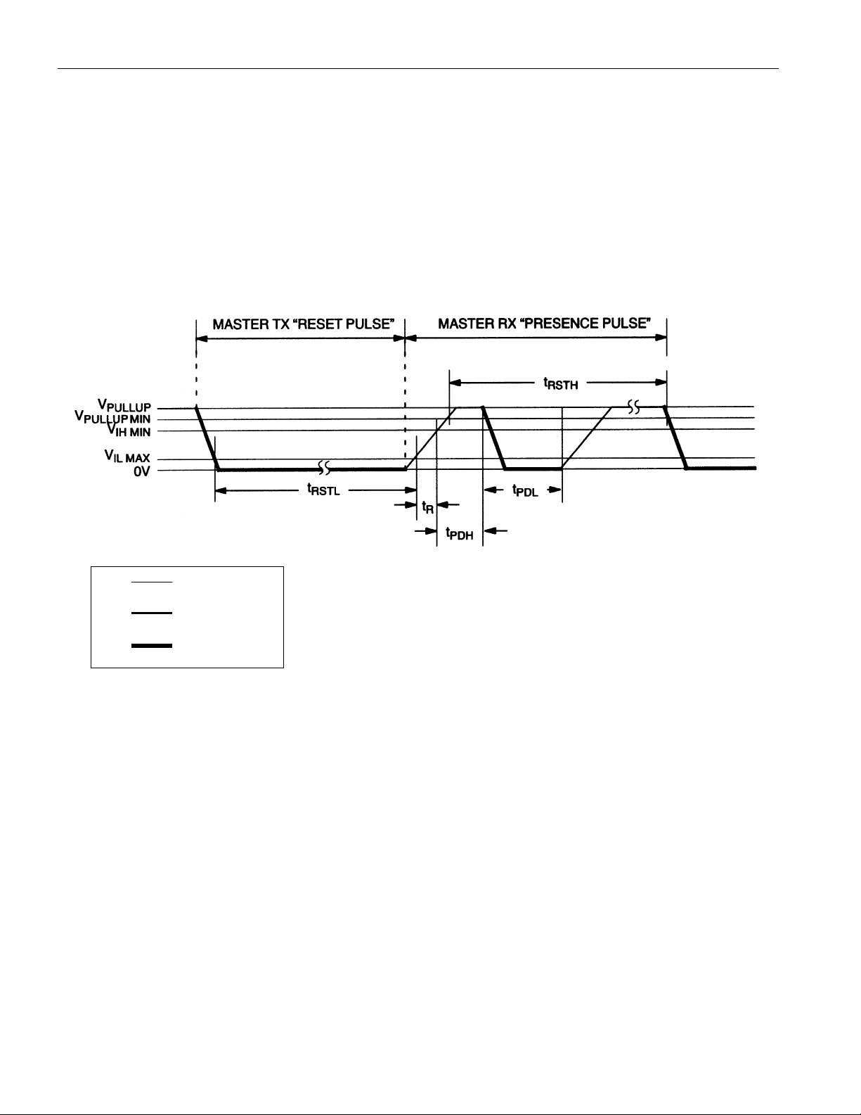
required to begin any communication with the DS2415 is shown in Figure 8. A Reset Pulse followed by a
Presence Pulse indicates the DS2415 is ready to send or receive data given the correct ROM command
and control function command. The bus master transmits (TX) a Reset Pulse (t
, minimum 480 µs).
RSTL
The bus master then releases the line and goes into receive mode (RX). The 1-Wire bus is pulled to a high
state via the pullup resistor. After detecting the rising edge on the data line, the DS2415 waits (t
µs) and then transmits the Presence Pulse (t
, 60-240 µs).
PDL
PDH
, 15-60
INITIALIZATION PROCEDURE “RESET AND PRESENCE PLUSES” Figure 8
RESISTOR
MASTER
DS2415
∗ In order not to mask interrupt signaling by other devices on the 1-Wire bus, t
480 µs ≤ t
480 µs ≤ t
15 µs ≤ t
60 µs ≤ t
< ∞ *
RSTL
< ∞ ( INCLUDES RECOVERY TIME)
RSTH
< 60 µs
PDH
< 240 µs
PDL
+ tR should always
RSTL
be less than 960 µs.
READ/WRITE TIME SLOTS
The definitions of write and read time slots are illustrated in Figure 9. All time slots are initiated by the
master driving the data line low. The falling edge of the data line synchronizes the DS2415 to the master
by triggering a delay circuit in the DS2415. During write time slots, the delay circuit determines when the
DS2415 will sample the data line. For a read data time slot, if a 0 is to be transmitted, the delay circuit
determines how long the DS2415 will hold the data line low overriding the 1 generated by the master. If
the data bit is a 1, the device will leave the read data time slot unchanged.
10 of 14
Page 11
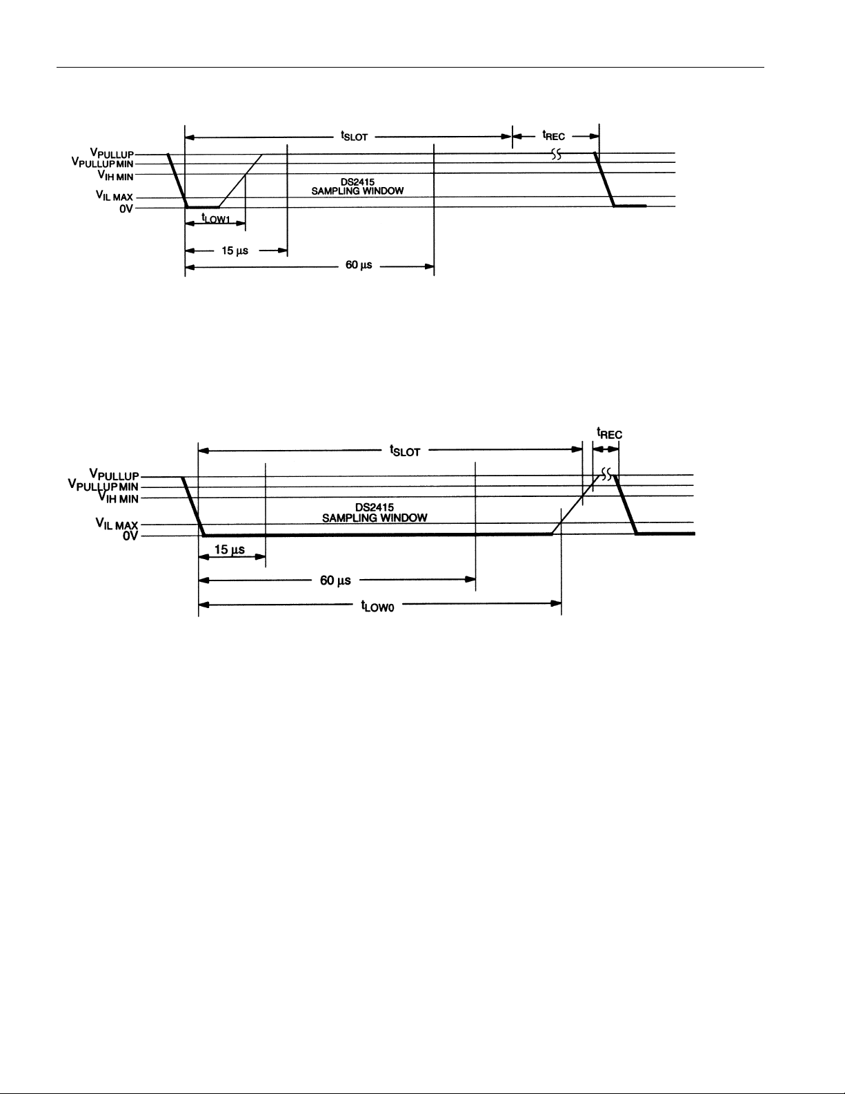
READ/WRITE TIMING DIAGRAM Figure 9
Write-1 Time Slot
DS2415
Write-0 Time Slot
60 µs ≤ t
1 µs ≤ t
1 µs ≤ t
60 µs ≤ t
1 µs ≤ t
SLOT
LOW1
REC
LOW0
REC
< 120 µs
< 15 µs
< ∞
< t
< ∞
SLOT
< 120 µs
11 of 14
Page 12
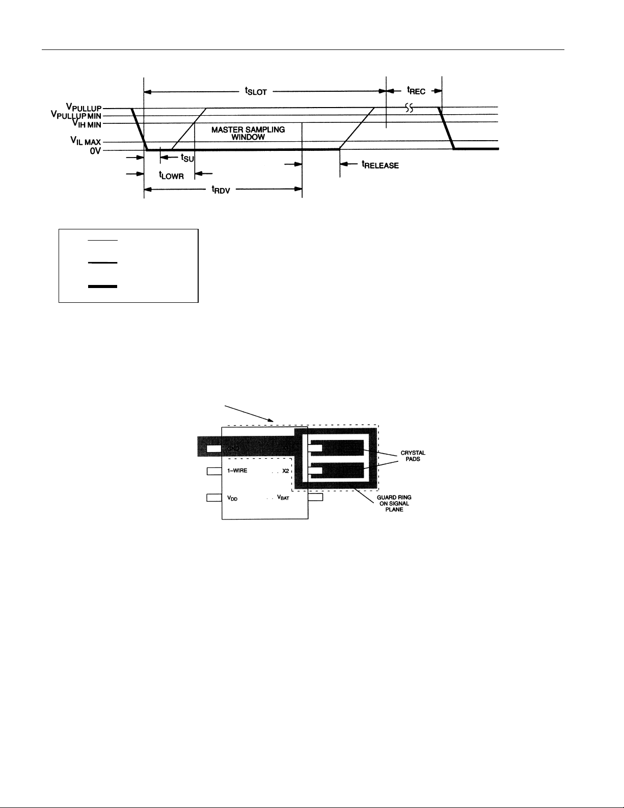
Read-data Time Slot
DS2415
RESISTOR
MASTER
DS2415
60 µs ≤ t
1 µs ≤ t
0 ≤ t
RELEASE
1 µs ≤ t
= 15 µs
t
RDV
t
< 1 µs
SU
SLOT
LOWR
REC
< 120 µs
< 15 µs
< 45 µs
< ∞
CRYSTAL PLACEMENT ON PCB Figure 10
LOCAL GROUND
PLANE BENEATH
SIGNAL PLANE
OR ON OTHER
SIDE OF PCB
12 of 14
Page 13

DS2415
ABSOLUTE MAXIMUM RATINGS*
Voltage on 1-Wire to Ground -0.5V to +7.0V
Operating Temperature -40°C to +85°C
Storage Temperature -55°C to +125°C
Soldering Temperature 260°C for 10 seconds
∗ This is a stress rating only and functional operation of the device at these or any other conditions
above those indicated in the operation sections of this specification is not implied. Exposure to
absolute maximum rating conditions for extended periods of time may affect reliability.
The Dallas Semiconductor DS2415 is built to the highest quality standards and manufactured for long
term reliability. All Dallas Semiconductor devices are made using the same quality materials and
manufacturing methods. However, the DS2415 is not exposed to environmental stresses, such as
burn-in, that some industrial applications require. For specific reliability information on this product,
please contact the factory in Dallas at (972) 371-4448.
DC ELECTRICAL CHARACTERISTICS
(-40°C to +85°C, V
= 2.5V to 6.0V, V
PUP
PARAMETER SYMBOL MIN TYP MAX UNITS NOTES
Logic 1 V
Logic 0 V
Output Logic Low @ 4mA V
Output Logic High V
Input Load Current
Operating Current (Osc. On) I
Quiescent Current (Osc. Off) I
BATQ3
Operating Current (Osc. On) I
Quiescent Current (Osc. Off) I
BATQ5
IH1
IL1
OL1
OH1
I
L1
BAT3
BAT5
2.2 6.0 V 1,12
-0.3 +0.8 V 1,7
0.4 V 1
V
PUP
5
250 nA 2,10
50 nA 2,9,10
450 nA 2,11
100 nA 2,9,11
= 2.5V to 5.5V)
BAT
V 1,3
µA
4
CAPACITANCE (TA = 25°C)
PARAMETER SYMBOL MIN TYP MAX UNITS NOTES
Capacitance 1-Wire C
IN
13 of 14
50 pF
Page 14

AC ELECTRICAL CHARACTERISTICS
(-40°C to +85°C, V
PARAMETER SYMBOL MIN TYP MAX UNITS NOTES
Time Slot
Write 1 Low Time
Write 0 Low Time
Read Low Time
Read Data Valid
Release Time
Read Data Setup
Recovery Time
Reset Time High
Reset Time Low
Presence Detect High
Presence Detect Low
t
SLOT
t
LOW1
t
LOW0
t
LOWR
t
RDV
t
RELEASE
t
SU
t
REC
t
RSTH
t
RSTL
t
PDH
t
PDL
= 2.5V to 6.0V, V
PUP
60 120
115
60 120
115
exactly 15
01545
1
1
480
480 960
15 60
60 240
= 2.5V to 5.5V)
BAT
µs
µs
µs
µs
µs
µs
µs
µs
µs
µs
µs
µs
NOTES:
1. All voltages are referenced to ground.
DS2415
6
5
8
2. Measured with outputs open.
3. V
= external pullup voltage.
PUP
4. Input load is to ground.
5. An additional reset or communication sequence cannot begin until the reset high time has expired.
6. Read data setup time refers to the time the bus master must pull the I/O line low to read a bit. Data is
guaranteed to be valid within 1 µs of this falling edge.
7. Under certain low voltage conditions V
IL1MAX
may have to be reduced to as much as 0.5V to always
guarantee a Presence Pulse.
8. The reset low time (t
) should be restricted to a maximum of 960 µs, to allow interrupt signaling,
RSTL
otherwise, it could mask or conceal interrupt pulses.
9. When V
10. At V
BAT
ramps up, the oscillator is always off.
BAT
= 3V ±10%
11. At V
12. V
IH1
= 5V ±10%
BAT
has to be V
-0.3V or higher.
BAT
14 of 14
 Loading...