

Page 1
www.dalsemi.com
DS21Q42
Enhanced QUAD T1 FRAMER
FEATURES
Four T1 DS1/ISDN–PRI/J1 framing
transceivers
All four framers are fully independent
Each of the four framers contain dual two–
frame elastic store slip buffers that can connect
to asynchronous backplanes up to 8.192 MHz
8–bit parallel control port that can be used
directly on either multiplexed or non–
multiplexed buses (Intel or Motorola)
Programmable output clocks for Fractional T1
Fully independent transmit and receive
functionality
Integral HDLC controller with 64-byte buffers
configurable for FDL or DS0 operation
Generates and detects in–band loop codes from
1 to 8 bits in length including CSU loop codes
Pin compatible with DS21Q44 E1 Enhanced
Quad E1 Framer
3.3V supply with 5V tolerant I/O; low power
CMOS
Available in 128–pin TQFP package
IEEE 1149.1 support
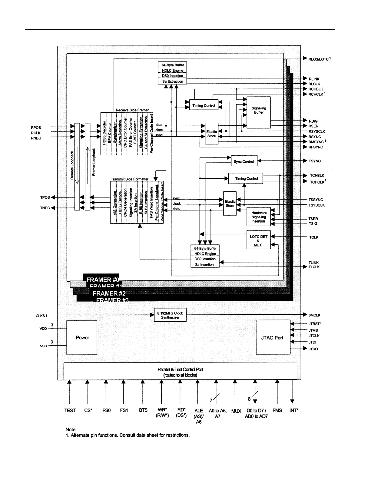
FUNCTIONAL DIAGRAM
Receive
Framer
Transmit
Formatter
FRAMER #0
FRAMER #1
FRAMER #2
FRAMER #3
Co ntro l Port
Elastic
Store
Elastic
Store
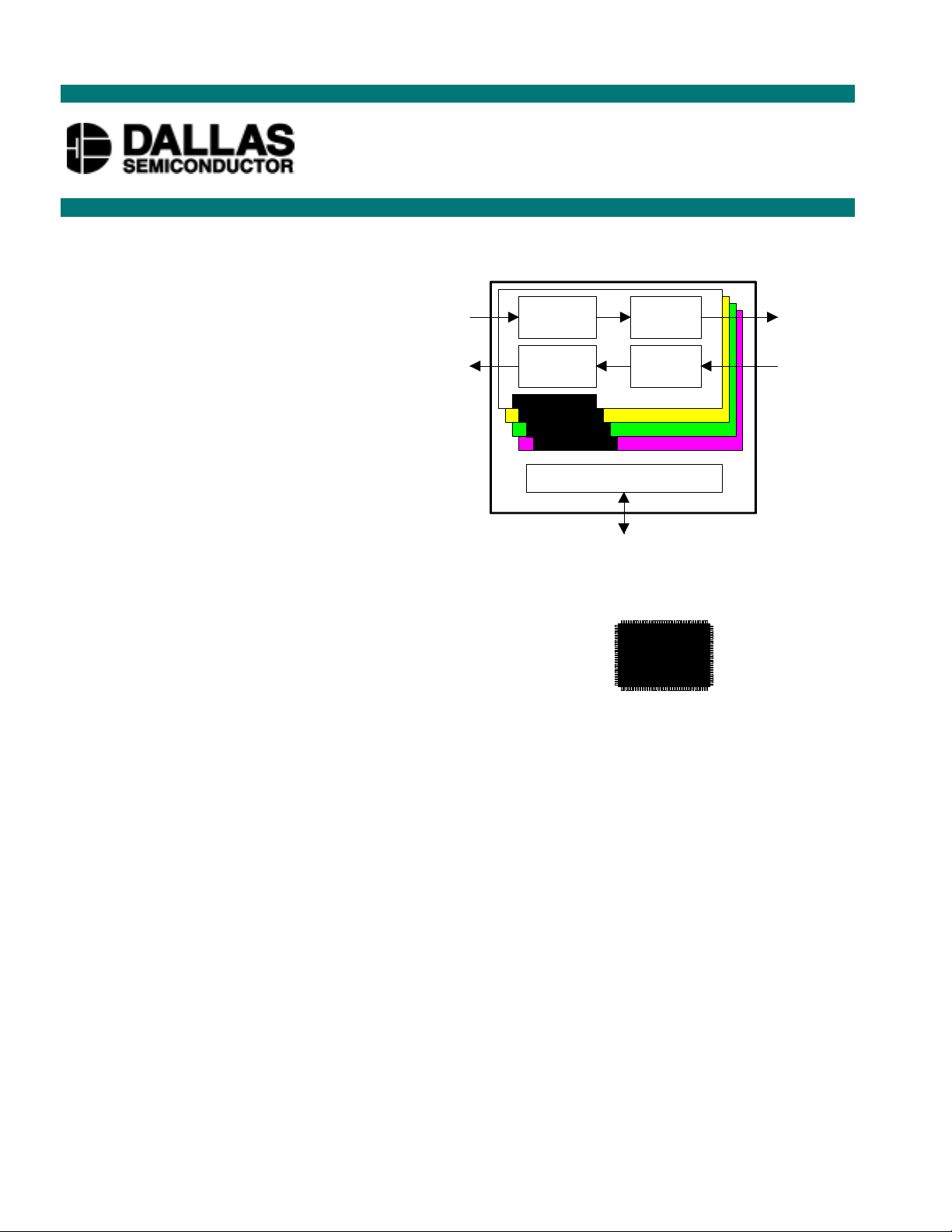
ACTUAL SIZE
QUAD
T1
FRAMER
ORDERING INFORMATION
DS21Q42T (00 C to 700 C)
DS21Q42TN (-40
0
C to +850 C)
DESCRIPTION
The DS21Q42 is an enhanced version of the DS21Q41B Quad T1 Framer. The DS21Q42 contains four
framers that are configured and read through a common microprocessor compatible parallel port. Each
framer consists of a receive framer, receive elastic stor e, transmit formatter and transmit elastic store. All
four framers in the DS21Q42 are totally independent, they do not share a common framing s ynchronizer.
Also the transmit and receive sides of each framer are totally independent. The dual two-frame elastic
stores contained in each of the four framers can be independ ently enabled and disabled as required. The
device fully meets all of the latest T1 specifications including ANSI T1.403–1995, ANSI T1.231–1993,
AT&T TR 62411 (12–90), AT&T TR54016, and ITU G.704 and G.706.
1 of 119 031500
Page 2

DS21Q42
1. INTRODUCTION
The DS21Q42 is a superset version of the popular DS21Q41 Quad T1 framer offering the new features
listed below. All of the original features of the DS21Q41 have been retained and software created for the
original device is transferable to the DS21Q42.
New Features
• Additional hardware signaling capability including:
– Receive signaling re-insertion to a backplane multiframe sync
– Availability of signaling in a separate PCM data stream
– Signaling freezing
– Interrupt generated on change of signaling data
• Full HDLC controller with 64–byte buffers in both transmit and receive paths. Configurable for FDL
orDS0 access
• Per–channel code insertion in both transmit and receive paths
• Ability to monitor one DS0 channel in both the transmit and receive paths
• RCL, RLOS, RRA, and RAIS alarms now interrupt on change of state
• Detects AIS-CI
• 8.192 MHz clock synthesizer
• Per–channel loopback
• Ability to calculate and check CRC6 according to the Japanese standard
• Ability to pass the F–Bit position through the elastic stores in the 2.048 MHz backplane mode
• IEEE 1149.1 support
Features
• Four T1 DS1/ISDN–PRI/J1 framing transceivers
• All four framers are fully independent
• Frames to D4, ESF, and SLC–96 R formats
• Each of the four framers contain dual two–frame elastic store slip buffers that can connect to
asynchronous backplanes up to 8.192 MHz
• 8–bit parallel control port that can be used directly on either multiplexed or non–multiplexed buses
(Intel or Motorola)
• Extracts and inserts robbed bit signaling
• Detects and generates yellow (RAI) and blue (AIS) alarms
• Programmable output clocks for Fractional T1
• Fully independent transmit and receive functionality
• Generates and detects in–band loop codes from 1 to 8 bits in length including CSU loop codes
• Contains ANSI one’s density monitor and enforcer
• Large path and line error counters including BPV, CV, CRC6, and framing bit errors
• Pin compatible with DS21Q44 E1 Enhanced Quad E1 Framer
• 3.3V supply with 5V tolerant I/O; low power CMOS
• Available in 128–pin TQFP package
2 of 119
Page 3

DS21Q42
Functional Description
The receive side framer locates D4 (SLC–96) or ESF multiframe boundaries as well as detects incoming
alarms including, carrier loss, loss of synchronization, blue (AIS) and yellow alarms. If needed, the
receive side elastic store can be en abled in order to absorb the ph ase and frequenc y differences between
the recovered T1 data stream and an asynchronous backplan e clock which is provided at the RSYSCLK
input. The clock applied at the RSYSCLK input can be either a 2.048 MHz clock or a 1.544 MHz clock.
The RSYSCLK can be a burst clock with speeds up to 8.192 MHz.
The transmit side of the DS21Q42 is totally independent from the receive side in both the clock
requirements and characteristics. Data off of a backplane can be passed through a transmit side elastic
store if necessary. The transmit formatter will provide the necessary frame/multiframe data overhead for
T1 transmission.
Reader’s Note:
This data sheet assumes a particular nomenclature of the T1 operating environment. In each 125 us frame,
there are 24 eight–bit channels plus a framing bit. It is assumed that the framing bit is sent first followed
by channel 1. Each channel is made up of eight bits which are numbered 1 to 8. Bit number 1 is the MSB
and is transmitted first. Bit number 8 is the LSB and is transmitted last. Throughout this data sheet, the
following abbreviations will be used:
D4 Superframe (12 frames per multiframe) Multiframe Structure
SLC–96 Subscriber Loop Carrier – 96 Channels (SLC–96 is an AT&T registered trademark)
ESF Extended Superframe (24 frames per multiframe) Multiframe Structure
B8ZS Bipolar with 8 Zero Substitution
CRC Cyclical Redundancy Check
Ft Terminal Framing Pattern in D4
Fs Signaling Framing Pattern in D4
FPS Framing Pattern in ESF
MF Multiframe
BOC Bit Oriented Code
HDLC High Level Data Link Control
FDL Facility Data Link
3 of 119
Page 4
DS21Q42 ENHANCED QUAD T1 FRAMER Figure 1-1
DS21Q42
4 of 119
Page 5

DS21Q42
TABLE OF CONTENTS
1. INTRODUCTION .............................................................................................................................. 2
2. DS21Q42 PIN DESCRIPTION ......................................................................................................... 8
3. DS21Q42 PIN FUNCTION DESCRIPTION ................................................................................ 15
4. DS21Q42 REGISTER MAP............................................................................................................. 22
5. PARALLEL PORT........................................................................................................................... 26
6. CONTROL, ID AND TEST REGISTERS.....................................................................................26
7. STATUS AND INFORMATION REGISTERS............................................................................. 37
8. ERROR COUNT REGISTERS....................................................................................................... 45
9. DS0 MONITORING FUNCTION................................................................................................... 48
10. SIGNALING OPERATION ............................................................................................................50
10.1. PROCESSOR BASED SIGNALING...................................................................................50
10.2. HARDWARE BASED SIGNALING ................................................................................... 52
11. PER–CHANNEL CODE (IDLE) GENERATION AND LOOPBACK....................................... 53
11.1. TRANSMIT SIDE CODE GENERATION ............................................................................ 53
11.1.1. Simple Idle Code Insertion and Per–Channel Loopback................................................. 54
11.1.2. Per–Channel Code Insertion ........................................................................................... .55
11.2. RECEIVE SIDE CODE GENERATION ................................................................................ 55
11.2.1. Simple Code Insertion ....................................................................................................55
11.2.2. Per–Channel Code Insertion ............................................................................................. 56
12. CLOCK BLOCKING REGISTERS.............................................................................................. 57
13. ELASTIC STORES OPERATION .............................................................................................. 58
13.1. RECEIVE SIDE....................................................................................................................... 58
13.2. TRANSMIT SIDE ................................................................................................................... 58
13.3. MINIMUM DELAY SYNCHRONOUS RSYSCLK/TSYSCLK MODE .............................. 59
5 of 119
Page 6

DS21Q42
14. HDLC CONTROLLER................................................................................................................... 59
14.1. HDLC FOR DS0S ................................................................................................................... 59
15. FDL/FS EXTRACTION AND INSERTION.................................................................................. 60
15.1. HDLC AND BOC CONTROLLER FOR THE FDL .............................................................. 60
15.1.1. General Overvie............................................................................................................ .60
15.1.2. Status Register for the HDLC........................................................................................ 61
15.1.3. HDLC/BOC Register Description ................................................................................. 63
15.2. LEGACY FDL SUPPORT ...................................................................................................... 71
15.2.1. Ov_2.1.71......................................................................................................................71
15.2.2. Receive Section............................................................................................................. 71
15.2.3. Transmit Section ........................................................................................................... 72
15.2.4. D4/SLC–96 OPERATION ............................................................................................ 73
16. PROGRAMMABLE IN–BAND CODE GENERATION AND DETECTION.......................... 73
17. TRANSMIT TRANSPARENCY.................................................................................................... 76
18. INTERLEAVED PCM BUS OPERATION................................................................................... 76
19. JTAG-BOUNDARY SCAN ARCHITECTURE AND TEST ACCESS PORT.......................... 79
19.1. DESCRIPTION ....................................................................................................................... 79
19.2. TAP CONTROLLER STATE MACHINE.............................................................................. 80
19.3. INSTRUCTION REGISTER AND INSTRUCTIONS ........................................................... 82
19.4. TEST REGISTERS .................................................................................................................84
20. TIMING DIAGRAMS...................................................................................................................... 89
21. OPERATING PARAMETERS .................................................................................................... 104
22. 128-PIN TQFP PACKAGE SPECIFICATIONS ........................................................................ 119
6 of 119
Page 7

DOCUMENT REVISION HISTORY
Revision Notes
12-22-98 Initial Release
DS21Q42
7 of 119
Page 8

2. DS21Q42 PIN DESCRIPTION
Pin Description Sorted by Pin Number Table 2-1
PIN SYMBOL TYPE DESCRIPTION
1 TCHBLK0 O Transmit Channel Block from Framer 0
2 TPOS0 O Transmit Bipolar Data from Framer 0
3 TNEG0 O Transmit Bipolar Data from Framer 0
4 RLINK0 O Receive Link Data from Framer 0
5 RLCLK0 O Receive Link Clock from Framer 0
6 RCLK0 I Receive Clock for Framer 0
7 RNEG0 I Receive Bipolar Data for Framer 0
8 RPOS0 I Receive Bipolar Data for Framer 0
9RSIG0
[RCHCLK0]
10 RCHBLK0 O Receive Channel Block from Framer 0
11 RSYSCLK0 I Receive System Clock for Elastic Store in Framer 0
12 RSYNC0 I/O Receive Sync for Framer 0
13 RSER0 O Receive Serial Data from Framer 0
14 VSS - Signal Ground
15 VDD - Positive Supply Voltage
16 SPARE1
[RMSYNC0]
17 RFSYNC0 O Receive Frame Sync from Framer 0
18 JTRST*
[RLOS/LOTC0]
19 TCLK0 I Transmit Clock for Framer 0
20 TLCLK0 O Transmit Link Clock from Framer 0
21 TSYNC0 I/O Transmit Sync for Framer 0
22 TLINK0 I Transmit Link Data for Framer 0
23 A0 I Address Bus Bit 0; LSB
24 A1 I Address Bus Bit 1
25 A2 I Address Bus Bit 2
26 A3 I Address Bus Bit 3
27 A4 I Address Bus Bit 4
28 A5 I Address Bus Bit 5
29 A6/ALE (AS) I Address Bus Bit 6; MSB or Address Latch Enable (Address
30 INT* O Receive Alarm Interrupt for all Four Framers
31 TSYSCLK1 I Transmit System Clock for Elastic Store in Framer 1
32 TSER1 I Transmit Serial Data for Framer 1
33 TSSYNC1 I Transmit Sync for Elastic Store in Framer 1
34 TSIG1
[TCHCLK1]
35 TCHBLK1 O Transmit Channel Block from Framer 1
36 TPOS1 O Transmit Bipolar Data from Framer 1
37 TNEG1 O Transmit Bipolar Data from Framer 1
38 RLINK1 O Receive Link Data from Framer 1
O
[O]
[O]
I [O] JTAG Reset [Receive Loss of Sync/Loss of Transmit clock
I [O] Transmit Signaling Input for Framer 1
Receive Signaling Output from Framer 0 [Receive Channel
Clock from Framer 0]
-
RESERVED - must be left unconnected for normal operation
[Receive Multiframe Sync from Framer 0]
from Framer 0]
Strobe)
[Transmit Channel Clock from Framer 1]
DS21Q42
8 of 119
Page 9

PIN SYMBOL TYPE DESCRIPTION
39 RLCLK1 O Receive Link Clock from Framer 1
40 RCLK1 I Receive Clock for Framer 1
41 RNEG1 I Receive Bipolar Data for Framer 1
42 RPOS1 I Receive Bipolar Data for Framer 1
43 RSIG1
[RCHCLK1]
O
[O]
Receive Signaling output from Framer 1
[Receive Channel Clock from Framer 1]
44 RCHBLK1 O Receive Channel Block from Framer 1
45 RSYSCLK1 I Receive System Clock for Elastic Store in Framer 1
46 A7 I Address Bus Bit 7
47 FMS I Framer Mode Select
48 RSYNC1 I/O Receive Sync for Framer 1
49 RSER1 O Receive Serial Data from Framer 1
50 JTMS
[RMSYNC1]
I
[O]
JTAG Test Mode Select
[Receive Multiframe Sync from Framer 1]
51 RFSYNC1 O Receive Frame Sync from Framer 1
52 JTCLK
[RLOS/LOTC1]
I
[O]
JTAG Test Clock
[Receive Loss of Sync/Loss of Transmit clock from Framer 1]
53 TCLK1 I Transmit Clock for Framer 1
54 TLCLK1 O Transmit Link Clock from Framer 1
55 TSYNC1 I/O Transmit Sync for Framer 1
56 TLINK1 I Transmit Link Data for Framer 1
57 TEST I 3-state Control for all Output and I/O Pins
58 FS0 I Framer Select 0 for Parallel Control Port
59 FS1 I Framer Select 1 for Parallel Control Port
60 CS* I Chip Select
61 BTS I Bus Type Select for Parallel Control Port
62 RD*/(DS*) I Read Input (Data Strobe)
63 WR*/(R/W*) I Write Input (Read/Write)
64 MUX I Non-Multiplexed or Multiplexed Bus Select
65 TSYSCLK2 I Transmit System Clock for Elastic Store in Framer 2
66 TSER2 I Transmit Serial Data for Framer 2
67 TSSYNC2 I Transmit Sync for Elastic Store in Framer 2
68 TSIG2
[TCHCLK2]
I
[O]
Transmit Signaling Input for Framer 2
[Transmit Channel Clock from Framer 2]
69 TCHBLK2 O Transmit Channel Block from Framer 2
70 TPOS2 O Transmit Bipolar Data from Framer 2
71 TNEG2 O Transmit Bipolar Data from Framer 2
72 RLINK2 O Receive Link Data from Framer 2
73 RLCLK2 O Receive Link Clock from Framer 2
74 RCLK2 I Receive Clock for Framer 2
75 RNEG2 I Receive Bipolar Data for Framer 2
76 RPOS2 I Receive Bipolar Data for Framer 2
77 RSIG2
[RCHCLK2]
O
[O]
Receive Signaling Output from Framer 2
[Receive Channel Clock from Framer 2]
78 VSS - Signal Ground
79 VDD - Positive Supply Voltage
80 RCHBLK2 O Receive Channel Block from Framer 2
DS21Q42
9 of 119
Page 10

PIN SYMBOL TYPE DESCRIPTION
81 RSYSCLK2 I Receive System Clock for Elastic Store in Framer 2
82 RSYNC2 I/O Receive Sync for Framer 2
83 RSER2 O Receive Serial Data from Framer 2
84 JTDI
[RMSYNC2]
I
[O]
JTAG Test Data Input
[Receive Multiframe Sync from Framer 2]
85 RFSYNC2 O Receive Frame Sync from Framer 2
86 JTDO
[RLOS/LOTC2]
O
[O]
JTAG Test Data Output
[Receive Loss of Sync/Loss of Transmit clock from Framer 2]
87 TCLK2 I Transmit Clock for Framer 2
88 TLCLK2 O Transmit Link Clock from Framer 2
89 TSYNC2 I/O Transmit Sync for Framer 2
90 TLINK2 I Transmit Link Data for Framer 2
91 TSYSCLK3 I Transmit System Clock for Elastic Store in Framer 3
92 TSER3 I Transmit Serial Data for Framer 3
93 TSSYNC3 I Transmit Sync for Elastic Store in Framer 3
94 TSIG3
[TCHCLK3]
I
[O]
Transmit Signaling Input for Framer 3
[Transmit Channel Clock from Framer 3]
95 TCHBLK3 O Transmit Channel Block from Framer 3
96 TPOS3 O Transmit Bipolar Data from Framer 3
97 TNEG3 O Transmit Bipolar Data from Framer 3
98 RLINK3 O Receive Link Data from Framer 3
99 RLCLK3 O Receive Link Clock from Framer 3
100 RCLK3 I Receive Clock for Framer 3
101 RNEG3 I Receive Bipolar Data for Framer 3
102 RPOS3 I Receive Bipolar Data for Framer 3
103 RSIG3
[RCHCLK3]
O
[O]
Receive Signaling Output from Framer 3
[Receive Channel Clock from Framer 3]
104 RCHBLK3 O Receive Channel Block from Framer 3
105 RSYSCLK3 I Receive System Clock for Elastic Store in Framer 3
106 RSYNC3 I/O Receive Sync for Framer 3
107 RSER3 O Receive Serial Data from Framer 3
108 8MCLK
[RMSYNC3]
O
[O]
8 MHz Clock
[Receive Multiframe Sync from Framer 3]
109 RFSYNC3 O Receive Frame Sync from Framer 3
110 VSS - Signal Ground
111 VDD - Positive Supply Voltage
112 CLKSI
[RLOS/LOTC3]
I
[O]
8MCLK Clock Reference Input
[Receive Loss of Sync/Loss of Transmit clock from Framer 3]
113 TCLK3 I Transmit Clock for Framer 3
114 TLCLK3 O Transmit Link Clock from Framer 3
115 TSYNC3 I/O Transmit Sync for Framer 3
116 TLINK3 I Transmit Link Data for Framer 3
117 D0 or AD0 I/O Data Bus Bit or Address/Data Bit 0; LSB
118 D1 or AD1 I/O Data Bus Bit or Address/Data Bit 1
119 D2 or AD2 I/O Data Bus Bit or Address/Data Bit 2
120 D3 or AD3 I/O Data Bus Bit or Address/Data Bit 3
121 D4 or AD4 I/O Data Bus Bit or Address/Data Bit 4
DS21Q42
10 of 119
Page 11

DS21Q42
PIN SYMBOL TYPE DESCRIPTION
122 D5 or AD5 I/O Data Bus Bit or Address/Data Bit 5
123 D6 or AD6 I/O Data Bus Bit or Address/Data Bit 6
124 D7 or AD7 I/O Data Bus Bit or Address/Data Bit 7; MSB
125 TSYSCLK0 I Transmit System Clock for Elastic Store in Framer 0
126 TSER0 I Transmit Serial Data for Framer 0
127 TSSYNC0 I Transmit Sync for Elastic Store in Framer 0
128 TSIG0
[TCHCLK0]
I
[O]
Transmit Signaling Input for Framer 0
[Transmit Channel Clock from Framer 0]
Note:
1. Brackets [ ] indicate pin function when the DS21Q42 is configured for emulation of the DS21Q41 B,
(FMS = 1).
11 of 119
Page 12

Pin Description Sorted by Pin Function, FMS = 0 Table 2-2
PIN SYMBOL TYPE DESCRIPTION
108 8MCLK O 8 MHz Clock
23 A0 I Address Bus Bit 0; LSB
24 A1 I Address Bus Bit 1
25 A2 I Address Bus Bit 2
26 A3 I Address Bus Bit 3
27 A4 I Address Bus Bit 4
28 A5 I Address Bus Bit 5
29 A6/ALE (AS) I Address Bus Bit 6; MSB or Address Latch Enable
(Address Strobe)
46 A7 I Address Bus Bit 7
61 BTS I Bus Type Select for Parallel Control Port
112 CLKSI I 8MCLK Clock Reference Input
60 CS* I Chip Select
117 D0 or AD0 I/O Data Bus Bit or Address/Data Bit 0; LSB
118 D1 or AD1 I/O Data Bus Bit or Address/Data Bit 1
119 D2 or AD2 I/O Data Bus Bit or Address/Data Bit 2
120 D3 or AD3 I/O Data Bus Bit or Address/Data Bit 3
121 D4 or AD4 I/O Data Bus Bit or Address/Data Bit 4
122 D5 or AD5 I/O Data Bus Bit or Address/Data Bit 5
123 D6 or AD6 I/O Data Bus Bit or Address/Data Bit 6
124 D7 or AD7 I/O Data Bus Bit or Address/Data Bit 7; MSB
47 FMS I Framer Mode Select
58 FS0 I Framer Select 0 for Parallel Control Port
59 FS1 I Framer Select 1 for Parallel Control Port
30 INT* O Receive Alarm Interrupt for all Four Framers
52 JTCLK I JTAG Test Clock
84 JTDI I JTAG Test Data Input
86 JTDO O JTAG Test Data Output
50 JTMS I JTAG Test Mode Select
18 JTRST* I JTAG Reset
64 MUX I Non-Multiplexed or Multiplexed Bus Select
10 RCHBLK0 O Receive Channel Block from Framer 0
44 RCHBLK1 O Receive Channel Block from Framer 1
80 RCHBLK2 O Receive Channel Block from Framer 2
104 RCHBLK3 O Receive Channel Block from Framer 3
6 RCLK0 I Receive Clock for Framer 0
40 RCLK1 I Receive Clock for Framer 1
74 RCLK2 I Receive Clock for Framer 2
100 RCLK3 I Receive Clock for Framer 3
62 RD*/(DS*) I Read Input (Data Strobe)
17 RFSYNC0 O Receive Frame Sync from Framer 0
51 RFSYNC1 O Receive Frame Sync from Framer 1
85 RFSYNC2 O Receive Frame Sync from Framer 2
109 RFSYNC3 O Receive Frame Sync from Framer 3
5 RLCLK0 O Receive Link Clock from Framer 0
DS21Q42
12 of 119
Page 13

DS21Q42
PIN SYMBOL TYPE DESCRIPTION
39 RLCLK1 O Receive Link Clock from Framer 1
73 RLCLK2 O Receive Link Clock from Framer 2
99 RLCLK3 O Receive Link Clock from Framer 3
4 RLINK0 O Receive Link Data from Framer 0
38 RLINK1 O Receive Link Data from Framer 1
72 RLINK2 O Receive Link Data from Framer 2
98 RLINK3 O Receive Link Data from Framer 3
7 RNEG0 I Receive Bipolar Data for Framer 0
41 RNEG1 I Receive Bipolar Data for Framer 1
75 RNEG2 I Receive Bipolar Data for Framer 2
101 RNEG3 I Receive Bipolar Data for Framer 3
8 RPOS0 I Receive Bipolar Data for Framer 0
42 RPOS1 I Receive Bipolar Data for Framer 1
76 RPOS2 I Receive Bipolar Data for Framer 2
102 RPOS3 I Receive Bipolar Data for Framer 3
13 RSER0 O Receive Serial Data from Framer 0
49 RSER1 O Receive Serial Data from Framer 1
83 RSER2 O Receive Serial Data from Framer 2
107 RSER3 O Receive Serial Data from Framer 3
9 RSIG0 O Receive Signaling Output from Framer 0
43 RSIG1 O Receive Signaling output from Framer 1
77 RSIG2 O Receive Signaling Output from Framer 2
103 RSIG3 O Receive Signaling Output from Framer 3
12 RSYNC0 I/O Receive Sync for Framer 0
48 RSYNC1 I/O Receive Sync for Framer 1
82 RSYNC2 I/O Receive Sync for Framer 2
106 RSYNC3 I/O Receive Sync for Framer 3
11 RSYSCLK0 I Receive System Clock for Elastic Store in Framer 0
45 RSYSCLK1 I Receive System Clock for Elastic Store in Framer 1
81 RSYSCLK2 I Receive System Clock for Elastic Store in Framer 2
105 RSYSCLK3 I Receive System Clock for Elastic Store in Framer 3
16 SPARE1 - RESERVED - must be left unconnected for normal operation
1 TCHBLK0 O Transmit Channel Block from Framer 0
35 TCHBLK1 O Transmit Channel Block from Framer 1
69 TCHBLK2 O Transmit Channel Block from Framer 2
95 TCHBLK3 O Transmit Channel Block from Framer 3
19 TCLK0 I Transmit Clock for Framer 0
53 TCLK1 I Transmit Clock for Framer 1
87 TCLK2 I Transmit Clock for Framer 2
113 TCLK3 I Transmit Clock for Framer 3
57 TEST I 3-state Control for all Output and I/O Pins
20 TLCLK0 O Transmit Link Clock from Framer 0
54 TLCLK1 O Transmit Link Clock from Framer 1
88 TLCLK2 O Transmit Link Clock from Framer 2
114 TLCLK3 O Transmit Link Clock from Framer 3
22 TLINK0 I Transmit Link Data for Framer 0
56 TLINK1 I Transmit Link Data for Framer 1
13 of 119
Page 14

PIN SYMBOL TYPE DESCRIPTION
90 TLINK2 I Transmit Link Data for Framer 2
116 TLINK3 I Transmit Link Data for Framer 3
3 TNEG0 O Transmit Bipolar Data from Framer 0
37 TNEG1 O Transmit Bipolar Data from Framer 1
71 TNEG2 O Transmit Bipolar Data from Framer 2
97 TNEG3 O Transmit Bipolar Data from Framer 3
2 TPOS0 O Transmit Bipolar Data from Framer 0
36 TPOS1 O Transmit Bipolar Data from Framer 1
70 TPOS2 O Transmit Bipolar Data from Framer 2
96 TPOS3 O Transmit Bipolar Data from Framer 3
126 TSER0 I Transmit Serial Data for Framer 0
32 TSER1 I Transmit Serial Data for Framer 1
66 TSER2 I Transmit Serial Data for Framer 2
92 TSER3 I Transmit Serial Data for Framer 3
128 TSIG0 I Transmit Signaling Input for Framer 0
34 TSIG1 I Transmit Signaling Input for Framer 1
68 TSIG2 I Transmit Signaling Input for Framer 2
94 TSIG3 I Transmit Signaling Input for Framer 3
127 TSSYNC0 I Transmit Sync for Elastic Store in Framer 0
33 TSSYNC1 I Transmit Sync for Elastic Store in Framer 1
67 TSSYNC2 I Transmit Sync for Elastic Store in Framer 2
93 TSSYNC3 I Transmit Sync for Elastic Store in Framer 3
21 TSYNC0 I/O Transmit Sync for Framer 0
55 TSYNC1 I/O Transmit Sync for Framer 1
89 TSYNC2 I/O Transmit Sync for Framer 2
115 TSYNC3 I/O Transmit Sync for Framer 3
125 TSYSCLK0 I Transmit System Clock for Elastic Store in Framer 0
31 TSYSCLK1 I Transmit System Clock for Elastic Store in Framer 1
65 TSYSCLK2 I Transmit System Clock for Elastic Store in Framer 2
91 TSYSCLK3 I Transmit System Clock for Elastic Store in Framer 3
15 VDD - Positive Supply Voltage
79 VDD - Positive Supply Voltage
111 VDD - Positive Supply Voltage
14 VSS - Signal Ground
78 VSS - Signal Ground
110 VSS - Signal Ground
63 WR*/(R/W*) I Write Input (Read/Write)
DS21Q42
14 of 119
Page 15

DS21Q42
3. DS21Q42 PIN FUNCTION DESCRIPTION
TRANSMIT SIDE PINS
Signal Name: TCLK
Signal Description: Transmit Clock
Signal Type: Input
A 1.544 MHz primary clock. Used to clock data through the transmit side formatter.
Signal Name: TSER
Signal Description: Transmit Serial Data
Signal Type: Input
Transmit NRZ serial data. Sampled on the falling edge of TCLK when the transmit side elastic store is
disabled. Sampled on the falling edge of TSYSCLK when the transmit side elastic store is enabled.
Signal Name: TCHCLK
Signal Description: Transmit Channel Clock
Signal Type: Output
A 192 KHz clock which pulses high during the LSB of each channel. Synchronous with TCLK when the
transmit side elastic store is disabled. Synchronous with TSYSCLK when the transmit side elastic store is
enabled. Useful for parallel to serial conversion of channel data. This function is available when FMS = 1
(DS21Q41 emulation).
Signal Name: TCHBLK
Signal Description: Transmit Channel Block
Signal Type: Output
A user programmable output that can be forced high or low during any of the 24 T1 channels.
Synchronous with TCLK when the transmit side elastic store is disabled. Synchronous with TSYSCLK
when the transmit side elastic store is enabled. Useful for blocking clocks to a serial UART or LAPD
controller in applications where not all T1 channels are used such as Fractional T1, 384 Kbps service, 768
Kbps or ISDN–PRI . Also useful for locating individual channels in drop–and–insert applications, for
external per–channel loopback, and for per–channel conditioning. See Section 12 for details.
Signal Name: TSYSCLK
Signal Description: Transmit System Clock
Signal Type: Input
1.544 MHz or 2.048 MHz clock. Only used when the transmit side elastic store function is enabled.
Should be tied low in applications that do not use the transmit side elastic store. Can be burst at rates up
to 8.192 MHz.
Signal Name: TLCLK
Signal Description: Transmit Link Clock
Signal Type: Output
4 KHz or 2 KHz (ZBTSI) demand clock for the TLINK input. See Section 15 for details.
15 of 119
Page 16

DS21Q42
Signal Name: TLINK
Signal Description: Transmit Link Data
Signal Type: Input
If enabled via TCR1.2, this pin will be sampled on the falling edge of TCLK for data insertion into either
the FDL stream (ESF) or the Fs–bit position (D4) or the Z–bit position (ZBTSI). See Section 15 for
details.
Signal Name: TSYNC
Signal Description: Transmit Sync
Signal Type: Input /Output
A pulse at this pin will establish either frame or multiframe boundaries for the transmit side. Via TCR2.2,
the DS21Q42 can be programmed to output either a frame or multiframe pulse at this pin. If this pin is set
to output pulses at frame boundaries, it can also be set via TCR2.4 to output double–wide pulses at
signaling frames. See Section 20 for details.
Signal Name: TSSYNC
Signal Description: Transmit System Sync
Signal Type: Input
Only used when the transmit side elastic store is enabled. A pulse at this pin will establish either frame or
multiframe boundaries for the transmit side. Should be tied low in applications that do not use the
transmit side elastic store.
Signal Name: TSIG
Signal Description: Transmit Signaling Input
Signal Type: Input
When enabled, this input will sample signaling bits for insertion into outgoing PCM T1 data stream.
Sampled on the falling edge of TCLK when the transmit side elastic store is disabled. Sampled on the
falling edge of TSYSCLK when the transmit side elastic store is enabled. This function is available when
FMS = 0.
Signal Name: TPOS
Signal Description: Transmit Positive Data Output
Signal Type: Output
Updated on the rising edge of TCLK with the bipolar data out of the transmit side formatter. Can be
programmed to source NRZ data via the Output Data Format (CCR1.6) control bit.
Signal Name: TNEG
Signal Description: Transmit Negative Data Output
Signal Type: Output
Updated on the rising edge of TCLK with the bipolar data out of the transmit side formatter.
16 of 119
Page 17

DS21Q42
RECEIVE SIDE PINS
Signal Name: RLINK
Signal Description: Receive Link Data
Signal Type: Output
Updated with either FDL data (ESF) or Fs bits (D4) or Z bits (ZBTSI) one RCLK before the start of a
frame. See Section 20 for details.
Signal Name: RLCLK
Signal Description: Receive Link Clock
Signal Type: Output
A 4 KHz or 2 KHz (ZBTSI) clock for the RLINK output.
Signal Name: RCHCLK
Signal Description: Receive Channel Clock
Signal Type: Output
A 192 KHz clock which pulses high during the LSB of each channel. Synchronous with RCLK when the
receive side elastic store is disabled. Synchronous with RSYSCLK when the receive side elastic store is
enabled. Useful for parallel to serial conversion of channel data. This function is available when FMS = 1
(DS21Q41 emulation).
Signal Name: RCHBLK
Signal Description: Receive Channel Block
Signal Type: Output
A user programmable output that can be forced high or low during any of the 24 T1 channels.
Synchronous with RCLK when the receive side elastic store is disabled. Synchronous with RSYSCLK
when the receive side elastic store is enabled. Useful for blocking clocks to a serial UART or LAPD
controller in applications where not all T1 channels are used such as Fractional T1, 384K bps service,
768K bps, or ISDN–PRI. Also useful for locating individual channels in drop–and–insert applications, for
external per–channel loopback, and for per–channel conditioning. See Section 12 for details.
Signal Name: RSER
Signal Description: Receive Serial Data
Signal Type: Output
Received NRZ serial data. Updated on rising edges of RCLK when the receive side elastic store is
disabled. Updated on the rising edges of RSYSCLK when the receive side elastic store is enabled.
Signal Name: RSYNC
Signal Description: Receive Sync
Signal Type: Input /Output
An extracted pulse, one RCLK wide, is output at this pin which identifies either frame (RCR2.4 = 0) or
multiframe (RCR2.4 = 1) boundaries. If set to output frame boundaries then via RCR2.5, RSYNC can
also be set to output double–wide pulses on signaling frames. If the receive side elastic store is enabled
via CCR1.2, then this pin can be enabled to be an input via RCR2.3 at which a frame or multiframe
boundary pulse is applied. See Section 20 for details.
Signal Name: RFSYNC
Signal Description: Receive Frame Sync
Signal Type: Output
An extracted 8 KHz pulse, one RCLK wide, is output at this pin which identifies frame boundaries.
17 of 119
Page 18

DS21Q42
Signal Name: RMSYNC
Signal Description: Receive Multiframe Sync
Signal Type: Output
An extracted pulse, one RSYSCLK wide, is output at this pin which identifies multiframe boundaries. If
the receive side elastic store is disabled, then this output will output multiframe boundaries associated
with RCLK. This function is available when FMS = 1 (DS21Q41 emulation).
Signal Name: RSYSCLK
Signal Description: Receive System Clock
Signal Type: Input
1.544 MHz or 2.048 MHz clock. Only used when the elastic store function is enabled. Should be tied low
in applications that do not use the elastic store. Can be burst at rates up to 8.192 MHz.
Signal Name: RSIG
Signal Description: Receive Signaling Output
Signal Type: Output
Outputs signaling bits in a PCM format. Updated on rising edges of RCLK when the receive side elastic
store is disabled. Updated on the rising edges of RSYSCLK when the receive side elastic store is enabled.
This function is available when FMS = 0.
Signal Name: RLOS/LOTC
Signal Description: Receive Loss of Sync / Loss of Transmit Clock
Signal Type: Output
A dual function output that is controlled by the CCR3.5 control bit. This pin can be programmed to either
toggle high when the synchronizer is searching for the frame and multiframe or to toggle high if the
TCLK pin has not been toggled for 5 usec. This function is available when FMS = 1 (DS21Q41
emulation).
Signal Name: CLKSI
Signal Description: 8 MHz Clock Reference
Signal Type: Input
A 1.544 MHz reference clock used in the generation of 8MCLK. This function is available when
FMS = 0.
Signal Name: 8MCLK
Signal Description: 8 MHz Clock
Signal Type: Output
A 8.192 MHz output clock that is referenced to the clock that is input at the CLKSI pin. This function is
available when FMS = 0.
18 of 119
Page 19

DS21Q42
Signal Name: RPOS
Signal Description: Receive Positive Data Input
Signal Type: Input
Sampled on the falling edge of RCLK for data to be clocked through the receive side framer. RPOS and
RNEG can be tied together for an NRZ interface. Connecting RPOS to RNEG disables the bipolar
violation monitoring circuitry.
Signal Name: RNEG
Signal Description: Receive Negative Data Input
Signal Type: Input
Sampled on the falling edge of RCLK for data to be clocked through the receive side framer. RPOS and
RNEG can be tied together for an NRZ interface. Connecting RPOS to RNEG disables the bipolar
violation monitoring circuitry.
Signal Name: RCLK
Signal Description: Receive Clock Input
Signal Type: Input
Clock used to clock data through the receive side framer.
PARALLEL CONTROL PORT PINS
Signal Name: INT*
Signal Description: Interrupt
Signal Type: Output
Flags host controller during conditions and change of conditions defined in the Status Registers 1 and 2
and the HDLC Status Register. Active low, open drain output.
Signal Name: FMS
Signal Description: Framer Mode Select
Signal Type: Input
Set low to select DS21Q42 feature set. Set high to select DS21Q41 emulation.
Signal Name: MUX
Signal Description: Bus Operation
Signal Type: Input
Set low to select non–multiplexed bus operation. Set high to select multiplexed bus operation.
Signal Name: D0 to D7/ AD0 to AD7
Signal Description: Data Bus or Address/Data Bus
Signal Type: Input /Output
In non–multiplexed bus operation (MUX = 0), serves as the data bus. In multiplexed bus operation (MUX
= 1), serves as a 8–bit multiplexed address / data bus.
Signal Name: A0 to A5, A7
Signal Description: Address Bus
Signal Type: Input
In non–multiplexed bus operation (MUX = 0), serves as the address bus. In multiplexed bus operation
(MUX = 1), these pins are not used and should be tied low.
19 of 119
Page 20

DS21Q42
Signal Name: ALE(AS)/A6
Signal Description: A6 or Address Latch Enable (Address Strobe)
Signal Type: Input
In non–multiplexed bus operation (MUX = 0), serves as address bit 6. In multiplexed bus operation
(MUX = 1), serves to demultiplex the bus on a positive–going edge.
Signal Name: BTS
Signal Description: Bus Type Select
Signal Type: Input
Strap high to select Motorola bus timing; strap low to select Intel bus timing. This pin controls the
function of the RD*(DS*), ALE(AS), and WR*(R/W*) pins. If BTS = 1, then these pins assume the
function listed in parenthesis ().
Signal Name: RD*(DS*)
Signal Description: Read Input (Data Strobe)
Signal Type: Input
RD* and DS* are active low signals. Note: DS is active high when MUX=1. Refer to bus timing
diagrams in section 21 .
Signal Name: FS0 AND FS1
Signal Description: Framer Selects
Signal Type: Input
Selects which of the four framers to be accessed.
Signal Name: CS*
Signal Description: Chip Select
Signal Type: Input
Must be low to read or write to the device. CS* is an active low signal.
Signal Name: WR*( R/W*)
Signal Description: Write Input(Read/Write)
Signal Type: Input
WR* is an active low signal.
TEST ACCESS PORT PINS
Signal Name: TEST
Signal Description: 3–State Control
Signal Type: Input
Set high to 3–state all output and I/O pins (including the parallel control port) when FMS = 1 or when
FMS = 0 and JTRST* is tied low. Set low for normal operation. Ignored when FMS = 0 and JTRST* = 1.
Useful in board level testing.
20 of 119
Page 21

DS21Q42
Signal Name: JTRST*
Signal Description: IEEE 1149.1 Test Reset
Signal Type: Input
This signal is used to asynchronously reset the test access port controller. At power up, JTRST* must be
set low and then high. This action will set the device into the DEVICE ID mode allowing normal device
operation. If boundary scan is not used and FMS = 0, this pin should be held low. This function is
available when FMS = 0. When FMS=1, this pin is held LOW internally. This pin is pulled up internally
by a 10K ohm resistor.
Signal Name: JTMS
Signal Description: IEEE 1149.1 Test Mode Select
Signal Type: Input
This pin is sampled on the rising edge of JTCLK and is used to place the test port into the various defined
IEEE 1149.1 states. This pin is pulled up internally by a 10K ohm resistor. If not used, this pin should be
left unconnected. This function is available when FMS = 0.
Signal Name: JTCLK
Signal Description: IEEE 1149.1 Test Clock Signal
Signal Type: Input
This signal is used to shift data into JTDI pin on the rising edge and out of JTDO pin on the falling edge.
If not used, this pin should be connected to VSS. This function is available when FMS = 0.
Signal Name: JTDI
Signal Description: IEEE 1149.1 Test Data Input
Signal Type: Input
Test instructions and data are clocked into this pin on the rising edge of JTCLK. This pin is pulled up
internally by a 10K ohm resistor. If not used, this pin should be left unconnected. This function is
available when FMS = 0.
Signal Name: JTDO
Signal Description: IEEE 1149.1 Test Data Output
Signal Type: Output
Test instructions and data are clocked out of this pin on the falling edge of JTCLK. If not used, this pin
should be left unconnected. This function is available when FMS = 0.
SUPPLY PINS
Signal Name: VDD
Signal Description: Positive Supply
Signal Type: Supply
2.97 to 3.63 volts.
Signal Name: VSS
Signal Description: Signal Ground
Signal Type: Supply
0.0 volts.
21 of 119
Page 22

4. DS21Q42 REGISTER MAP
Register Map Sorted by Address Table 4-1
ADDRESS R/W REGISTER NAME
00 R/W HDLC Control HCR
01 R/W HDLC Status HSR
02 R/W HDLC Interrupt Mask HIMR
03 R/W Receive HDLC Information RHIR
04 R/W Receive Bit Oriented Code RBOC
05 R Receive HDLC FIFO RHFR
06 R/W Transmit HDLC Information THIR
07 R/W Transmit Bit Oriented Code TBOC
08 W Transmit HDLC FIFO THFR
09 – Not used (set to 00H)
0A R/W Common Control 7 CCR7
0B – Not used (set to 00H)
0C – Not used (set to 00H)
0D – Not used (set to 00H)
0E – Not used (set to 00H)
0F R Device ID IDR
10 R/W Receive Information 3 RIR3
11 R/W Common Control 4 CCR4
12 R/W In–Band Code Control IBCC
13 R/W Transmit Code Definition TCD
14 R/W Receive Up Code Definition RUPCD
15 R/W Receive Down Code Definition RDNCD
16 R/W Transmit Channel Control 1 TCC1
17 R/W Transmit Channel Control 2 TCC2
18 R/W Transmit Channel Control 3 TCC3
19 R/W Common Control 5 CCR5
1A R Transmit DS0 Monitor TDS0M
1B R/W Receive Channel Control 1 RCC1
1C R/W Receive Channel Control 2 RCC2
1D R/W Receive Channel Control 3 RCC3
1E R/W Common Control 6 CCR6
1F R Receive DS0 Monitor RDS0M
20 R/W Status 1 SR1
21 R/W Status 2 SR2
22 R/W Receive Information 1 RIR1
23 R Line Code Violation Count 1 LCVCR1
24 R Line Code Violation Count 2 CVCR2
25 R Path Code Violation Count 1 PCVCR1
26 R Path Code violation Count 2 PCVCR2
27 R Multiframe Out of Sync Count 2 MOSCR2
28 R Receive FDL Register RFDL
29 R/W Receive FDL Match 1 RMTCH1
ABBREVIATION
DS21Q42
REGISTER
22 of 119
Page 23

REGISTER
ADDRESS R/W REGISTER NAME
ABBREVIATION
2A R/W Receive FDL Match 2 RMTCH2
2B R/W Receive Control 1 RCR1
2C R/W Receive Control 2 RCR2
2D R/W Receive Mark 1 RMR1
2E R/W Receive Mark 2 RMR2
2F R/W Receive Mark 3 RMR3
30 R/W Common Control 3 CCR3
31 R/W Receive Information 2 RIR2
32 R/W Transmit Channel Blocking 1 TCBR1
33 R/W Transmit Channel blocking 2 TCBR2
34 R/W Transmit Channel Blocking 3 TCBR3
35 R/W Transmit Control 1 TCR1
36 R/W Transmit Control 2 TCR2
37 R/W Common Control 1 CCR1
38 R/W Common Control 2 CCR2
39 R/W Transmit Transparency 1 TTR1
3A R/W Transmit Transparency 2 TTR2
3B R/W Transmit Transparency 3 TTR3
3C R/W Transmit Idle 1 TIR1
3D R/W Transmit Idle 2 TIR2
3E R/W Transmit Idle 3 TIR3
3F R/W Transmit Idle Definition TIDR
40 R/W Transmit Channel 9 TC9
41 R/W Transmit Channel 10 TC10
42 R/W Transmit Channel 11 TC11
43 R/W Transmit Channel 12 TC12
44 R/W Transmit Channel 13 TC13
45 R/W Transmit Channel 14 TC14
46 R/W Transmit Channel 15 TC15
47 R/W Transmit Channel 16 TC16
48 R/W Transmit Channel 17 TC17
49 R/W Transmit Channel 18 TC18
4A R/W Transmit Channel 19 TC19
4B R/W Transmit Channel 20 TC20
4C R/W Transmit Channel 21 TC21
4D R/W Transmit Channel 22 TC22
4E R/W Transmit Channel 23 TC23
4F R/W Transmit Channel 24 TC24
50 R/W Transmit Channel 1 TC1
51 R/W Transmit Channel 2 TC2
52 R/W Transmit Channel 3 TC3
53 R/W Transmit Channel 4 TC4
54 R/W Transmit Channel 5 TC5
55 R/W Transmit Channel 6 TC6
56 R/W Transmit Channel 7 TC7
57 R/W Transmit Channel 8 TC8
DS21Q42
23 of 119
Page 24

REGISTER
ADDRESS R/W REGISTER NAME
ABBREVIATION
58 R/W Receive Channel 17 RC17
59 R/W Receive Channel 18 RC18
5A R/W Receive Channel 19 RC19
5B R/W Receive Channel 20 RC20
5C R/W Receive Channel 21 RC21
5D R/W Receive Channel 22 RC22
5E R/W Receive Channel 23 RC23
5F R/W Receive Channel 24 RC24
60 R Receive Signaling 1 RS1
61 R Receive Signaling 2 RS2
62 R Receive Signaling 3 RS3
63 R Receive Signaling 4 RS4
64 R Receive Signaling 5 RS5
65 R Receive Signaling 6 RS6
66 R Receive Signaling 7 RS7
67 R Receive Signaling 8 RS8
68 R Receive Signaling 9 RS9
69 R Receive Signaling 10 RS10
6A R Receive Signaling 11 RS11
6B R Receive Signaling 12 RS12
6C R/W Receive Channel Blocking 1 RCBR1
6D R/W Receive Channel Blocking 2 RCBR2
6E R/W Receive Channel Blocking 3 RCBR3
6F R/W Interrupt Mask 2 IMR2
70 R/W Transmit Signaling 1 TS1
71 R/W Transmit Signaling 2 TS2
72 R/W Transmit Signaling 3 TS3
73 R/W Transmit Signaling 4 TS4
74 R/W Transmit Signaling 5 TS5
75 R/W Transmit Signaling 6 TS6
76 R/W Transmit Signaling 7 TS7
77 R/W Transmit Signaling 8 TS8
78 R/W Transmit Signaling 9 TS9
79 R/W Transmit Signaling 10 TS10
7A R/W Transmit Signaling 11 TS11
7B R/W Transmit Signaling 12 TS12
7C – Not used (set to 00H)
7D R/W Test 1 TEST1 (set to 00h)
7E R/W Transmit FDL Register TFDL
7F R/W Interrupt Mask Register 1 IMR1
80 R/W Receive Channel 1 RC1
81 R/W Receive Channel 2 RC2
82 R/W Receive Channel 3 RC3
83 R/W Receive Channel 4 RC4
84 R/W Receive Channel 5 RC5
85 R/W Receive Channel 6 RC6
DS21Q42
24 of 119
Page 25

REGISTER
ADDRESS R/W REGISTER NAME
ABBREVIATION
86 R/W Receive Channel 7 RC7
87 R/W Receive Channel 8 RC8
88 R/W Receive Channel 9 RC9
89 R/W Receive Channel 10 RC10
8A R/W Receive Channel 11 RC11
8B R/W Receive Channel 12 RC12
8C R/W Receive Channel 13 RC13
8D R/W Receive Channel 14 RC14
8E R/W Receive Channel 15 RC15
8F R/W Receive Channel 16 RC16
90 R/W Receive HDLC DS0 Control Register 1 RDC1
91 R/W Receive HDLC DS0 Control Register 2 RDC2
92 R/W Transmit HDLC DS0 Control Register 1 TDC1
93 R/W Transmit HDLC DS0 Control Register 2 TDC2
94 R/W Interleave Bus Operation Register IBO
95 – Not used (set to 00H)
96 R/W Test 2 TEST2 (set to 00h)
97 – Not used (set to 00H)
98 – Not used (set to 00H)
99 – Not used (set to 00H)
9A – Not used (set to 00H)
9B – Not used (set to 00H)
9C – Not used (set to 00H)
9D – Not used (set to 00H)
9E – Not used (set to 00H)
9F – Not used (set to 00H)
DS21Q42
Notes:
1. Test Registers 1 and 2 are used only by the factory; these registers must be cleared (set to all zeros) on
power– up initialization to insure proper operation.
2. Register banks AxH, BxH, CxH, DxH, ExH, and FxH are not accessible.
25 of 119
Page 26

DS21Q42
5. PARALLEL PORT
The DS21Q42 is controlled via either a nonmultiplexed (MUX = 0) or a multiplexed (MUX = 1) bus b y
an external microcontroller or microprocessor. The DS21Q42 can operate with either Intel or Motorola
bus timing configurations. If the BTS pin is tied low, Intel timing will be selected; if tied high, Motorola
timing will be selected. All Motorola bus signals are listed in parenthesis (). See the timing diagrams in
the A.C. Electrical Characteristics in Section 21 for more details.
6. CONTROL, I D AND TEST REGISTERS
The operation of each framer within the DS21Q42 is configured via a set of eleven control registers.
Typically, the control registers are only accessed when the system is first powered up. Once a channel in
the DS21Q42 has been initialized, the control registers will only need to be accessed when there is a
change in the system configuration. There are two Receive Control Register (RCR1 and RCR2), two
Transmit Control Registers (TCR1 and TCR2), and seven Common Control Registers (CCR1 to CCR7).
Each of the eleven registers are described in this section. There is a device Identification Register (IDR)
at address 0Fh. The MSB of this read–only register is fixed to a zero indicating that the DS21Q42 is
present. The E1 pin–for–pin compatible version of the DS21Q42 is the DS21Q44 and it also has an ID
register at address 0Fh and the user c an read the MSB to determine which chip is present since in the
DS21Q42 the MSB will be set to a zero and in the DS21Q44 it will be set to a one. The lower four bits of
the IDR are used to display the die revision of the chip.
Power–Up Sequence
The DS21Q42 does not automatically clear its register space on power–up. After the supplies are stable,
each of the four framer’s register space should be confi gured for operation by writing to all of the internal
registers. This includes setting the Test and all unused registers to 00Hex.
This can be accomplished using a two-pass approach on each framer within the DS21Q42.
1. Clear framer’s register space by writing 00H to the addresses 00H through 09FH.
2. Program required registers to achieve desired operating mode.
Note:
When emulating the DS21Q41 feature set (FMS = 1), the full address space (00H through 09FH) must be
initialized. DS21Q41 emulation requires address pin A7 to be used.
Finally, after the TSYSCLK and RSYSCLK inputs are stable, the ESR bit should be toggled from a zero
to a one (this step can be skipped if the elastic stores are disabled).
26 of 119
Page 27

DS21Q42
IDR: DEVICE IDENTIFICATION REGISTER (Address=0F Hex)
(MSB) (LSB)
T1E1 0 0 0 ID3 ID2 ID1 ID0
SYMBOL POSITION NAME AND DESCRIPTION
T1E1 IDR.7
T1 or E1 Chip Determination Bit.
0=T1 chip
1=E1 chip
ID3 IDR.3 Chip Revision Bit 3. MSB of a decimal code that represents the chip
revision.
ID2 IDR.1
ID1 IDR.2
Chip Revision Bit 2.
Chip Revision Bit 1.
ID0 IDR.0 Chip Revision Bit 0. LSB of a decimal code that represents the chip
revision.
RCR1: RECEIVE CONTROL REGISTER 1 (Address=2B Hex)
(MSB) (LSB)
LCVCRF ARC OOF1 OOF2 SYNCC SYNCT SYNCE RESYNC
SYMBOL POSITION NAME AND DESCRIPTION
LCVCRF RCR1.7
Line Code Violation Count Register Function Select.
0 = do not count excessive zeros
1 = count excessive zeros
ARC RCR1.6
Auto Resync Criteria.
0 = Resync on OOF or RCL event
1 = Resync on OOF only
OOF1 RCR1.5
Out Of Frame Select 1.
0 = 2/4 frame bits in error
1 = 2/5 frame bits in error
OOF2 RCR1.4
Out Of Frame Select 2.
0 = follow RCR1.5
1 = 2/6 frame bits in error
SYNCC RCR1.3
Sync Criteria.
In D4 Framing Mode.
0 = search for Ft pattern, then search for Fs pattern
1 = cross couple Ft and Fs pattern
In ESF Framing Mode.
0 = search for FPS pattern only
1 = search for FPS and verify with CRC6
SYNCT RCR1.2
Sync Time.
0 = qualify 10 bits
1 = qualify 24 bits
SYNCE RCR1.1
Sync Enable.
0 = auto resync enabled
1 = auto resync disabled
RESYNC RCR1.0 Resync. When toggled from low to high, a resynchronization of the
receive side framer is initiated. Must be cleared and set again for a
subsequent resync.
27 of 119
Page 28

DS21Q42
RCR2: RECEIVE CONTROL REGISTER 2 (Address=2C Hex)
(MSB) (LSB)
RCS RZBTSI RSDW RSM RSIO RD4YM FSBE MOSCRF
SYMBOL POSITION NAME AND DESCRIPTION
RCS RCR2.7 Receive Code Select. See Section 11 for more details.
0 = idle code (7F Hex)
1 = digital milliwatt code (1E/0B/0B/1E/9E/8B/8B/9E Hex)
RZBTSI RCR2.6
RSDW RCR2.5 RSYNC Double–Wide. (note: this bit must be set to zero when
RSM RCR2.4 RSYNC Mode Select. (A Don’t Care if RSYNC is programmed as
RSIO RCR2.3 RSYNC I/O Select. (note: this bit must be set to zero when CCR1.2
RD4YM RCR2.2
FSBE RCR2.1
MOSCRF RCR2.0
Receive Side ZBTSI Enable.
0 = ZBTSI disabled
1 = ZBTSI enabled
RCR2.4 = 1 or when RCR2.3 = 1)
0 = do not pulse double wide in signaling frames
1 = do pulse double wide in signaling frames
an input)
0 = frame mode (see the timing in Section 20)
1 = multiframe mode (see the timing in Section 20)
= 0)
0 = RSYNC is an output
1 = RSYNC is an input (only valid if elastic store enabled)
Receive Side D4 Yellow Alarm Select.
0 = zeros in bit 2 of all channels
1 = a one in the S–bit position of frame 12
PCVCR Fs–Bit Error Report Enable.
0 = do not report bit errors in Fs–bit position; only Ft bit position
1 = report bit errors in Fs–bit position as well as Ft bit position
Multiframe Out of Sync Count Register Function Select.
0 = count errors in the framing bit position
1 = count the number of multiframes out of sync
28 of 119
Page 29

DS21Q42
TCR1: TRANSMIT CONTROL REGISTER 1 (Address=35 Hex)
(MSB) (LSB)
LOTCMC TFPT TCPT TSSE GB7S TFDLS TBL TYEL
SYMBOL POSITION NAME AND DESCRIPTION
LOTCMC TCR1.7 Loss Of Transmit Clock Mux Control. Determines whether the
transmit side formatter should switch to RCLK if the TCLK input
should fail to transition (see Figure 1.1 for details).
0 = do not switch to RCLK if TCLK stops
1 = switch to RCLK if TCLK stops
TFPT TCR1.6 Transmit F–Bit Pass Through. (see note below)
0 = F bits sourced internally
1 = F bits sampled at TSER
TCPT TCR1.5 Transmit CRC Pass Through. (see note below)
0 = source CRC6 bits internally
1 = CRC6 bits sampled at TSER during F–bit time
TSSE TCR1.4 Software Signaling Insertion Enable. (see note below)
0 = no signaling is inserted in any channel
1 = signaling is inserted in all channels from the TS1-TS12 registers
(the TTR registers can be used to block insertion on a channel by
channel basis)
GB7S TCR1.3 Global Bit 7 Stuffing. (see note below)
0 = allow the TTR registers to determine which channels containing
all zeros are to be Bit 7 stuffed
1 = force Bit 7 stuffing in all zero byte channels regardless of how
the
TTR registers are programmed
TFDLS TCR1.2 TFDL Register Select. (see note below)
0 = source FDL or Fs bits from the internal TFDL register (legacy
FDL support mode)
1 = source FDL or Fs bits from the internal HDLC/BOC controller
or the TLINK pin
TBL TCR1.1 Transmit Blue Alarm. (see note below)
0 = transmit data normally
1 = transmit an unframed all one’s code at TPOS and TNEG
TYEL TCR1.0 Transmit Yellow Alarm. (see note below)
0 = do not transmit yellow alarm
1 = transmit yellow alarm
Note:
For a description of how the bits in TCR1 affect the transmit side formatter, see Figure 20-15.
29 of 119
Page 30

DS21Q42
TCR2: TRANSMIT CONTROL REGISTER 2 (Address=36 Hex)
(MSB) (LSB)
TEST1 TEST0 TZBTSI TSDW TSM TSIO TD4YM TB7ZS
SYMBOL POSITION NAME AND DESCRIPTION
TEST1 TCR2.7 Test Mode Bit 1 for Output Pins. See Table 6–1.
TEST0 TCR2.6 Test Mode Bit 0 for Output Pins. See Table 6–1.
TZBTSI TCR2.5
TSDW TCR2.4 TSYNC Double–Wide. (note: this bit must be set to zero when
TSM TCR2.3
TSIO TCR2.2
TD4YM TCR2.1
TB7ZS TCR2.0
Transmit Side ZBTSI Enable.
0 = ZBTSI disabled
1 = ZBTSI enabled
TCR2.3=1 or when TCR2.2=0)
0 = do not pulse double–wide in signaling frames
1 = do pulse double–wide in signaling frames
TSYNC Mode Select.
0 = frame mode (see the timing in Section 20)
1 = multiframe mode (see the timing in Section 20)
TSYNC I/O Select.
0 = TSYNC is an input
1 = TSYNC is an output
Transmit Side D4 Yellow Alarm Select.
0 = zeros in bit 2 of all channels
1 = a one in the S–bit position of frame 12
Transmit Side Bit 7 Zero Suppression Enable.
0 = no stuffing occurs
1 = Bit 7 force to a one in channels with all zeros
OUTPUT PIN TEST MODES Table 6-1
TEST 1 TEST 0 EFFECT ON OUTPUT PINS
0 0 operate normally
0 1 force all of the selected framer’s output pins 3–state (excludes other
framers I/O pins and parallel port pins)
1 0 force all of the selected framer’s output pins low (excludes other
framers I/O pins and parallel port pins)
1 1 force all of the selected framer’s output pins high (excludes other
framers I/O pins and parallel port pins)
30 of 119
Page 31

DS21Q42
CCR1: COMMON CONTROL REGISTER 1 (Address=37 Hex)
(MSB) (LSB)
TESE ODF RSAO TSCLKM RSCLKM RESE PLB FLB
SYMBOL POSITION NAME AND DESCRIPTION
TESE CCR1.7
ODF CCR1.6
RSAO CCR1.5 Receive Signaling All One’s. This bit should not be enabled if
TSCLKM CCR1.4
RSCLKM CCR1.3
RESE CCR1.2
PLB CCR1.1
FLB CCR1.0
Transmit Elastic Store Enable.
0 = elastic store is bypassed
1 = elastic store is enabled
Output Data Format.
0 = bipolar data at TPOS and TNEG
1 = NRZ data at TPOS; TNEG = 0
hardware signaling is being utilized. See Section 10 for more details.
0 = allow robbed signaling bits to appear at RSER
1 = force all robbed signaling bits at RSER to one
TSYSCLK Mode Select.
0 = if TSYSCLK is 1.544 MHz
1 = if TSYSCLK is 2.048 MHz
RSYSCLK Mode Select.
0 = if RSYSCLK is 1.544 MHz
1 = if RSYSCLK is 2.048 MHz
Receive Elastic Store Enable.
0 = elastic store is bypassed
1 = elastic store is enabled
Payload Loopback.
0 = loopback disabled
1 = loopback enabled
Framer Loopback.
0 = loopback disabled
1 = loopback enabled
Payload Loopback
When CCR1.1 is set to a one, the DS21Q42 will be forced into Payload LoopBack (PLB). Normally, this
loopback is only enabled when ESF framing is being performed but can be enabled also in D4 framing
applications. In a PLB situation, the DS21Q42 will loop the 192 bits of payload data (with BPVs
corrected) from the receive section back to the transmit section. The FPS framing pattern, CRC6
calculation, and the FDL bits are not looped back, they are reinserted by the DS21Q42. When PLB is
enabled, the following will occur:
1. Data will be transmitted from the TPOS and TNEG pins synchronous with RCLK instead of TCLK
2. All of the receive side signals will continue to operate normally
3. The TCHCLK and TCHBLK signals are forced low
4. Data at the TSER, and TSIG pins is ignored
5. The TLCLK signal will become synchronous with RCLK instead of TCLK.
31 of 119
Page 32

DS21Q42
Framer Loopback
When CCR1.0 is set to a one, the DS21Q42 will enter a Framer LoopBack (FLB) mode. This loopback is
useful in testing and debugging applications. In FLB, the DS21Q42 will loop data from the transmit side
back to the receive side. When FLB is enabled, the following will occur:
1. an unframed all one’s code will be transmitted at TPOS and TNEG
2. data at RPOS and RNEG will be ignored
3. all receive side signals will take on timing synchronous with TCLK instead of RCLK
Please note that it is not acceptable to have RCLK tied to TCLK during this loopback because this will
cause an unstable condition.
CCR2: COMMON CONTROL REGISTER 2 (Address=38 Hex)
(MSB) (LSB)
TFM TB8ZS TS LC96 TZSE RFM RB8ZS RSLC96 RZSE
SYMBOL POSITION NAME AND DESCRIPTION
TFM CCR2.7
TB8ZS CCR2.6
TSLC96 CCR2.5 Transmit SLC–96 / Fs–Bit Insertion Enable. Only set this bit to a
TZSE CCR2.4 Transmit FDL Zero Stuffer Enable. Set this bit to zero if using
RFM CCR2.3
RB8ZS CCR2.2
RSLC96 CCR2.1 Receive SLC–96 Enable. Only set this bit to a one in D4/SLC–96
Transmit Frame Mode Select.
0 = D4 framing mode
1 = ESF framing mode
Transmit B8ZS Enable.
0 = B8ZS disabled
1 = B8ZS enabled
one in D4 framing applications. Must be set to one to source the Fs
pattern. See Section 15 for details.
0 = SLC–96/Fs–bit insertion disabled
1 = SLC–96/Fs–bit insertion enabled
the internal HDLC/BOC controller instead of the legacy support for
the FDL. See Section 15 for details.
0 = zero stuffer disabled
1 = zero stuffer enabled
Receive Frame Mode Select.
0 = D4 framing mode
1 = ESF framing mode
Receive B8ZS Enable.
0 = B8ZS disabled
1 = B8ZS enabled
framing applications. See Section 15 for details.
0 = SLC–96 disabled
1 = SLC–96 enabled
32 of 119
Page 33

DS21Q42
SYMBOL POSITION NAME AND DESCRIPTION
RZSE CCR2.0 Receive FDL Zero Destuffer Enable. Set this bit to zero if using
the internal HDLC/BOC controller instead of the legacy support for
the FDL. See Section 15 for details.
0 = zero destuffer disabled
1 = zero destuffer enabled
CCR3: COMMON CONTROL REGISTER 3 (Address=30 Hex)
(MSB) LSB)
RESMDM TCLKSRC RLOSF RSMS PDE ECUS TLOOP TESMDM
SYMBOL POSITION NAME AND DESCRIPTION
RESMDM CCR3.7 Receive Elastic Store Minimum Delay Mode. See Section 13 for
details.
0 = elastic stores operate at full two frame depth
1 = elastic stores operate at 32–bit depth
TCLKSRC CCR3.6 Transmit Clock Source Select. This function allows the user to
internally select RCLK as the clock source for the transmit side
formatter.
0 = Transmit side formatter clocked with signal applied at TCLK
pin.
LOTC Mux function is operational (TCR1.7)
1 = Transmit side formatter clocked with RCLK.
RLOSF CCR3.5 Function of the RLOS/LOTC Output. Active only when FMS = 1
(DS21Q41 emulation).
0 = Receive Loss of Sync (RLOS)
1 = Loss of Transmit Clock (LOTC)
RSMS CCR3.4 RSYNC Multiframe Skip Control. Useful in framing format
conversions from D4 to ESF. This function is not available when
the receive side elastic store is enabled.
0 = RSYNC will output a pulse at every multiframe
1 = RSYNC will output a pulse at every other multiframe note: for
this
bit to have any affect, the RSYNC must be set to output multiframe
pulses (RCR2.4=1 and RCR2.3=0).
PDE CCR3.3
ECUS CCR3.2 Error Counter Update Select. See Section 8 for details.
TLOOP CCR3.1 Transmit Loop Code Enable. See Section 16 for details.
Pulse Density Enforcer Enable.
0 = disable transmit pulse density enforcer
1 = enable transmit pulse density enforcer
0 = update error counters once a second
1 = update error counters every 42 ms (333 frames)
0 = transmit data normally
1 = replace normal transmitted data with repeating code as defined
in TCD register
33 of 119
Page 34

DS21Q42
SYMBOL POSITION NAME AND DESCRIPTION
TESMDM CCR3.0 Transmit Elastic Store Minimum Delay Mode. See Section 13
for details.
0 = elastic stores operate at full two frame depth
1 = elastic stores operate at 32–bit depth
Pulse Density Enforcer
The Framer always examines both the transmit and receive data streams for violations of the following
rules which are required by ANSI T1.403:
– no more than 15 consecutive zeros
– at least N ones in each and every time window of 8 x (N +1) bits where N = 1 through 23
Violations for the transmit and receive data streams are reported in the RIR2.0 and RIR2.1 bits
respectively. When the CCR3.3 is set to one, the DS21Q42 will force the transmitted stream to meet this
requirement no matter the content of the transmitted stream. When running B8ZS, the CCR3.3 bit should
be set to zero since B8ZS encoded data streams cannot violate the pulse density requirements.
CCR4: COMMON CONTROL REGISTER 4 (Address=11 Hex)
(MSB) (LSB)
RSRE RPCSI RFSA1 RFE RFF THSE TPCSI TIRFS
SYMBOL POSITION NAME AND DESCRIPTION
RSRE CCR4.7 Receive Side Signaling Re–Insertion Enable. See Section 10 for
details.
0 = do not re–insert signaling bits into the data stream presented at
the RSER pin
1 = reinsert the signaling bits into data stream presented at the
RSER pin
RPCSI CCR4.6 Receive Per–Channel Signaling Insert. See Section 10 for more
details.
0 = do not use RCHBLK to determine which channels should have
signaling re–inserted
1 = use RCHBLK to determine which channels should have
signaling re–inserted
RFSA1 CCR4.5 Receive Force Signaling All Ones. See Section 10 for more
details.
0 = do not force extracted robbed–bit signaling bit positions to a one
1 = force extracted robbed–bit signaling bit positions to a one
RFE CCR4.4 Receive Freeze Enable. See Section 10 for details.
0 = no freezing of receive signaling data will occur
1 = allow freezing of receive signaling data at RSIG (and RSER if
CCR4.7 = 1).
34 of 119
Page 35

DS21Q42
SYMBOL POSITION NAME AND DESCRIPTION
RFF CCR4.3 Receiv e Forc e Freez e. Freezes receive side signaling at RSIG (and
RSER if CCR4.7=1); will override Receive Freeze Enable (RFE).
See Section 10 for details.
0 = do not force a freeze event
1 = force a freeze event
THSE CCR4.2 Transmit Hardware Signaling Insertion Enable. See Section 10
for details.
0 = do not insert signaling from the TSIG pin into the data stream
presented at the TSER pin.
1 = Insert the signaling from the TSIG pin into data stream
presented at the TSER pin.
TPCSI CCR4.1 Transmit Per–Channel Signaling Insert. See Section 10 for
details.
0 = do not use TCHBLK to determine which channels should have
signaling inserted from the TSIG pin.
1 = use TCHBLK to determine which channels should have
signaling inserted from the TSIG pin.
TIRFS CCR4.0 Transmit Idle Registers (TIR) Function Select. See Section 11
for timing details.
0 = TIRs define in which channels to insert idle code
1 = TIRs define in which channels to insert data from RSER (i.e.,
Per = Channel Loopback function)
CCR5: COMMON CONTROL REGISTER 5 (Address=19 Hex)
(MSB) (LSB)
TJC – – TCM4 TCM3 TCM2 TCM1 TCM0
SYMBOL POSITION NAME AND DESCRIPTION
TJC CCR5.7
– CCR5.6 Not Assigned. Must be set to zero when written.
– CCR5.5 Not Assigned. Must be set to zero when written.
TCM4 CCR5.4 Transmit Channel Monitor Bit 4. MSB of a channel decode that
TCM3 CCR5.3
TCM2 CCR5.2
TCM1 CCR5.1
TCM0 CCR5.0 Transmit Channel Monitor Bit 0. LSB of the channel decode.
Transmit Japanese CRC6 Enable.
0 = use ANSI/AT&T/ITU CRC6 calculation (normal operation)
1 = use Japanese standard JT–G704 CRC6 calculation
determines which transmit channel data will appear in the TDS0M
register. See Section 9 for details.
Transmit Channel Monitor Bit 3.
Transmit Channel Monitor Bit 2.
Transmit Channel Monitor Bit 1.
35 of 119
Page 36

DS21Q42
CCR6: COMMON CONTROL REGISTER 6 (Address=1E Hex)
(MSB) (LSB)
RJC RESALGN TESALGN RCM4 RCM3 RCM2 RCM1 RCM0
SYMBOL POSITION NAME AND DESCRIPTION
RJC CCR6.7
RESALGN CCR6.6 Receive Elastic Store Align. Setting this bit from a zero to a one
TESALGN CCR6.5 Transmit Elastic Store Align. Setting this bit from a zero to a one
RCM4 CCR6.4 Receive Channel Monitor Bit 4. MSB of a channel decode that
RCM3 CCR6.3
RCM2 CCR6.2
RCM1 CCR6.1
RCM0 CCR6.0 Receive Channel Monitor Bit 0. LSB of the channel decode.
Receive Japanese CRC6 Enable.
0 = use ANSI/AT&T/ITU CRC6 calculation (normal operation)
1 = use Japanese standard JT–G704 CRC6 calculation
may force the receive elastic store’s write/read pointers to a
minimum separation of half a frame. No action will be taken if the
pointer separation is already greater or equal to half a frame. If
pointer separation is less then half a frame, the command will be
executed and data will be disrupted. Should be toggled after
RSYSCLK has been applied and is stable. Must be cleared and set
again for a subsequent align. See Section 13 for details.
may force the transmit elastic store’s write/read pointers to a
minimum separation of half a frame. No action will be taken if the
pointer separation is already greater or equal to half a frame. If
pointer separation is less then half a frame, the command will be
executed and data will be disrupted. Should be toggled after
TSYSCLK has been applied and is stable. Must be cleared and set
again for a subsequent align. See Section 13 for details.
determines which receive channel data will appear in the RDS0M
register. See Section 9 for details.
Receive Channel Monitor Bit 3.
Receive Channel Monitor Bit 2.
Receive Channel Monitor Bit 1.
36 of 119
Page 37

DS21Q42
CCR7: COMMON CONTROL REGISTER 7 (Address=0A Hex)
(MSB) (LSB)
- RLB RESR TESR - - - -
SYMBOL POSITION NAME AND DESCRIPTION
– CCR7.7 Not Assigned. Should be set to zero when written to.
RLB CCR7.6
RESR CCR7.5 Receive Elastic Store Reset. Setting this bit from a zero to a one
TESR CCR7.4 Transmit Elastic Store Reset. Setting this bit from a zero to a one
– CCR7.3 Not Assigned. Should be set to zero when written to.
– CCR7.2 Not Assigned. Should be set to zero when written to.
– CCR7.1 Not Assigned. Should be set to zero when written to.
– CCR7.0 Not Assigned. Should be set to zero when written to.
Remote Loopback.
0 = loopback disabled
1 = loopback enabled
will force the receive elastic store to a depth of one frame. Receive
data is lost during the reset. Should be toggled after RSYSCLK has
been applied and is stable. Do not leave this bit set high.
will force the transmit elastic store to a depth of one frame.
Transmit data is lost during the reset. Should be toggled after
TSYSCLK has been applied and is stable. Do not leave this bit set
high.
Remote Loopback
When CCR7.6 is set to a one, the DS21Q42 will be forced into Remote LoopBack (RLB). In this
loopback, data input via the RPOS and RNEG pins will be transmitted back to the TPOS and TNEG pins.
Data will continue to pass through the receive side framer of the DS21Q42 as it would normally and the
data from the transmit side formatter will be ignored. Please see Figure 1-1 for more details.
7. STATUS AND INFORMATION REGISTERS
There is a set of nine registers per channel that contain information on the current real time status of a
framer in the DS21Q42, Status Register 1 (SR1), Status Register 2 (SR2), Receive Information Registers
1 to 3 (RIR1/RIR2/RIR3) and a set of four registers for the onboard HDLC and BOC controller. The
specific details on the four registers pertaining to the HDLC and BOC controller are covered in Section
15 but they operate the same as the other status registers in the DS21Q42 and this operation is described
below.
When a particular event has occurred (or is occurring), the appropriate bit in one of these nine registers
will be set to a one. All of the bits in SR1, SR2, RIR1, RIR2, and RIR3 registers operate in a latched
fashion. This means that if an event or an alarm occurs and a bit is set to a one in any of the registers, it
will remain set until the user reads that bit. The bit will be cleared when it is read and it will not be set
again until the event has occurred again (or in the case of the RBL, RYEL, LRCL, and RLOS alarms, the
bit will remain set if the alarm is still present). There are bits in the four HDLC and BOC status registers
that are not latched and these bits are listed in Section 15.
37 of 119
Page 38

DS21Q42
The user will always precede a read of any of the nine registers with a write. The byte written to the
register will inform the DS21Q42 which bits the user wishes to read and have cleared. The user will write
a byte to one of these registers, with a one in the bit positions he or she wishes to read and a zero in the
bit positions he or she does not wish to obtain the latest information on. When a one is written to a bit
location, the read register will be updated with the latest information. When a zero is written to a bit
position, the read register will not be updated and the previous value will be held. A write to the status
and information registers will be immediately followed by a read of the same register. The read result
should be logically AND’ed with the mask byte that was just written and this value should be written
back into the same register to insure that bit does indeed clear. This second write step is necessary
because the alarms and events in the status registers occur asynchronously in respect to their access via
the parallel port. This write–read– write scheme allows an external microcontroller or microprocessor to
individually poll certain bits without disturbing the other bits in the register. This operation is key in
controlling the DS21Q42 with higher–order software languages.
The SR1, SR2, and FDLS registers have the unique ability to initiate a hardware interrupt via the INT*
output pin. Each of the alarms and events in the SR1, SR2, and HSR can be either masked or unmasked
from the interrupt pin via the Interrupt Mask Register 1 (IMR1), Interrupt Mask Register 2 (IMR2), and
HDLC Interrupt Mask Register (HIMR) respectively. The FIMR register is covered in Section 15. The
INTERRUPT STATUS REGISTER can be used to determine which framer is requesting interrupt
servicing and the type of the request: status or the HDLC controller.
The interrupts caused by alarms in SR1 (namely RYEL, RCL, RBL, RLOS and LOTC) act differently
than the interrupts caused by events in SR1 and SR2 (namely LUP, LDN, RSLIP, RMF, TMF, SEC,
RFDL, TFDL, RMTCH, RAF, and RSC) and HIMR. The alarm caused interrupts will force the INT* pin
low whenever the alarm changes state (i.e., the alarm goes active or inactive according to the set/clear
criteria in Table 7-1). The INT* pin will be allowed to return high (if no other interrupts are present)
when the user reads the alarm bit that caused the interrupt to occur even if the alarm is still present.
The event caused interrupts will force the INT* pin low when the event occurs. The INT* pin will be
allowed to return high (if no other interrupts are present) when the user reads the event bit that caused the
interrupt to occur.
ISR: INTERRUPT STATUS REGISTER (Any address from A0H to FFH)
(MSB) (LSB)
F3HDLC F3SR F2HDLC F2SR F1HDLC F1SR F0HDLC F0SR
SYMBOL POSITION NAME AND DESCRIPTION
F3HDLC ISR.7
F3SR ISR.6
F2HDLC ISR.5
FRAMER 3 HDLC CONTROLLER INTERRUPT
REQUEST.
0 = No interrupt request pending.
1 = Interrupt request pending.
FRAMER 3 SR1 or SR2 INTERRUPT REQUEST.
0 = No interrupt request pending.
1 = Interrupt request pending.
FRAMER 2 HDLC CONTROLLER INTERRUPT
REQUEST.
0 = No interrupt request pending.
1 = Interrupt request pending.
38 of 119
Page 39

SYMBOL POSITION NAME AND DESCRIPTION
F2SR ISR.4
FRAMER 2 SR1 or SR2 INTERRUPT REQUEST.
0 = No interrupt request pending.
1 = Interrupt request pending.
F1HDLC ISR.3
FRAMER 1 HDLC CONTROLLER INTERRUPT
REQUEST.
0 = No interrupt request pending.
1 = Interrupt request pending.
F1SR ISR.2
FRAMER 1 SR1 or SR2 INTERRUPT REQUEST.
0 = No interrupt request pending.
1 = Interrupt request pending.
F0HDLC ISR.1
FRAMER 0 HDLC CONTROLLER INTERRUPT
REQUEST.
0 = No interrupt request pending.
1 = Interrupt request pending.
F0SR ISR 0
FRAMER 0 SR1 or SR2 INTERRUPT REQUEST.
0 = No interrupt request pending.
1 = Interrupt request pending.
RIR1: RECEIVE INFORMATION REGISTER 1 (Address=22 Hex)
DS21Q42
(MSB) (LSB)
COFA 8ZD 16ZD RESF RESE SEFE B8ZS FBE
SYMBOL POSITION NAME AND DESCRIPTION
COFA RIR1.7 Change of Frame Alignment. Set when the last resync
resulted in a change of frame or multiframe alignment.
8ZD RIR1.6 Eight Zero Detect. Set when a string of at least eight
consecutive zeros (regardless of the length of the string) have
been received at RPOS and RNEG.
16ZD RIR1.5 Sixteen Zero Detect. Set when a string of at least sixteen
consecutive zeros (regardless of the length of the string) have
been received at RPOS and RNEG.
RESF RIR1.4 Receive Elastic Store Full. Set when the receive elastic store
buffer fills and a frame is deleted.
RESE RIR1.3 Receive Elastic Store Empty. Set when the receive elastic
store buffer empties and a frame is repeated.
SEFE RIR1.2 Severely Errored Framing Event. Set when 2 out of 6
framing bits (Ft or FPS) are received in error.
B8ZS RIR1.1 B8ZS Code Word Detect. Set when a B8ZS code word is
detected at RPOS and RNEG independent of whether the
B8ZS mode is selected or not via CCR2.6. Useful for
automatically setting the line coding.
FBE RIR1.0 Frame Bit Error. Set when a Ft (D4) or FPS (ESF) framing
bit is received in error.
39 of 119
Page 40

DS21Q42
RIR2: RECEIVE INFORMATION REGISTER 2 (Address=31 Hex)
(MSB) (LSB)
RLOSC RCLC TESF TESE TSLIP RBLC RPDV TPDV
SYMBOL POSITION NAME AND DESCRIPTION
RLOSC RIR2.7 Receive Loss of Sync Clear. Set when the framer achieves
synchronization; will remain set until read.
RCLC RIR2.6 Receive Carrier Loss Clear. Set when the carrier signal is
restored; will remain set until read. See Table 7-1.
TESF RIR2.5 Transmit Elastic Store Full. Set when the transmit elastic
store buffer fills and a frame is deleted.
TESE RIR2.4 Transmit Elastic Store Empty. Set when the transmit elastic
store buffer empties and a frame is repeated.
TSLIP RIR2.3 Transmit Elastic Store Slip Occurrence. Set when the
transmit elastic store has either repeated or deleted a frame.
RBLC RIR2.2 Receive Blue Alarm Clear. Set when the Blue Alarm (AIS)
is no longer detected; will remain set until read. See Table 7-1.
RPDV RIR2.1 Receive Pulse Density Violation. Set when the receive data
stream does not meet the ANSI T1.403 requirements for pulse
density.
TPDV RIR2.0 Transmit Pulse Density Violation. Set when the transmit
data stream does not meet the ANSI T1.403 requirements for
pulse density.
RIR3: RECEIVE INFORMATION REGISTER 3 (Address=10 Hex)
(MSB) (LSB)
---
SYMBOL POSITION NAME AND DESCRIPTION
– RIR3.7 Not Assigned. Could be any value when read.
– RIR3.6 Not Assigned. Could be any value when read.
– RIR3.5 Not Assigned. Could be any value when read.
LORC RIR3.4 Loss of Receive Clock. Set when the RCLK pin has not
– RIR3.3 Not Assigned. Could be any value when read.
– RIR3.2 Not Assigned. Could be any value when read.
– RIR3.1 Not Assigned. Could be any value when read.
RAIS-CI RIR3.0 Receive AIS-CI Detect. Set when the AIS-CI pattern is
LORC - - - RAIS-CI
transitioned for at least 2 us (3 us ˜˜1 us).
detected.
40 of 119
Page 41

DS21Q42
SR1: STATUS REGISTER 1 (Address=20 Hex)
(MSB) (LSB)
LUP LDN LOTC RSLIP RBL RYEL RCL RLOS
SYMBOL POSITION NAME AND DESCRIPTION
LUP SR1.7 Loop Up Code Detected. Set when the loop up code as
defined in the RUPCD register is being received. See Section
16 for details.
LDN SR1.6 Loop Down Code Detected. Set when the loop down code as
defined in the RDNCD register is being received. See Section
16 for details.
LOTC SR1.5 Loss of Transmit Clock. Set when the TCLK pin has not
transitioned for one channel time (or 5.2 us). Will force the
RLOS/LOTC pin high if enabled via CCR3.5. Also will force
transmit side formatter to switch to RCLK if so enabled via
TCR1.7.
RSLIP SR1.4 Receive Elastic Store Slip Occurrence. Set when the receive
elastic store has either repeated or deleted a frame.
RBL SR1.3 Receive Blue Alarm. Set when an unframed all one’s code is
received at RPOS and RNEG.
RYEL SR1.2 Receive Yellow Alarm. Set when a yellow alarm is received
at RPOS and RNEG.
RCL SR1.1 Receive Carrier Loss. Set when a red alarm is received at
RPOS and RNEG.
RLOS SR1.0 Receive Loss of Sync. Set when the device is not
synchronized to the receive T1 stream.
41 of 119
Page 42

ALARM CRITERIA Table 7-1
ALARM SET CRITERIA CLEAR CRITERIA
Blue Alarm (AIS)
(see note 1 below)
when over a 3 ms window, 5 or
less zeros are received
DS21Q42
when over a 3 ms window, 6 or
more zeros are received
Yellow Alarm (RAI)
1. D4 bit 2 mode(RCR2.2=0)
2. D4 12th F–bit mode
(RCR2.2=1; this mode is also
referred to as the “Japanese
Yellow Alarm”)
3. ESF mode when 16 consecutive patterns of
Red Alarm (RCL) (this alarm is
also referred to as Loss Of
Signal)
when bit 2 of 256 consecutive
channels is set to zero for at least
254 occurrences
when the 12th framing bit is set
to one for two consecutive
occurrences
00FF appear in the FDL
when 192 consecutive zeros are
received
when bit 2 of 256 consecutive
channels is set to zero for less
than 254 occurrences
when the 12th framing bit is set
to zero for two consecutive
occurrences
when 14 or less patterns of 00FF
hex out of 16 possible appear in
the FDL
when 14 or more ones out of 112
possible bit positions are received
starting with the first one
received
Notes:
1. The definition of Blue Alarm (or Alarm Indication Signal) is an unframed all ones signal. Blue alarm
detectors should be able to operate properly in the presence of a 10–3 error rate and they should not
falsely trigger on a framed all ones signal. The blue alarm criteria in the DS21Q42 has been set to
achieve this performance. It is recommended that the RBL bit be qualified with the RLOS bit.
2. ANSI specifications use a different nomenclature than the DS21Q42 does; the following terms are
equivalent:
RBL = AIS
RCL = LOS
RLOS = LOF
RYEL = RAI
42 of 119
Page 43

DS21Q42
SR2: STATUS REGISTER 2 (Address=21 Hex)
(MSB) (LSB)
RMF TMF SEC RFDL TFDL RMTCH RAF RSC
SYMBOL POSITION NAME AND DESCRIPTION
RMF SR2.7 Receive Multiframe. Set on receive multiframe boundaries.
TMF SR2.6 Transmit Multiframe. Set on transmit multiframe boundaries.
SEC SR2.5 One Second Timer. Set on increments of one second based on
RCLK; will be set in increments of 999 ms, 999 ms, and 1002
ms every 3 seconds.
RFDL SR2.4 Receive FDL Buffer Full. Set when the receive FDL buffer
(RFDL) fills to capacity (8 bits).
TFDL SR2.3 Transmit FDL Buffer Empty. Set when the transmit FDL
buffer (TFDL) empties.
RMTCH SR2.2 Receive FDL Match Occurrence. Set when the RFDL
matches either RMTCH1 or RMTCH2.
RAF SR2.1 Receive FDL Abort. Set when eight consecutive one’s are
received in the FDL.
RSC SR2.0 Receive Signaling Change. Set when the DS21Q42 detects a
change of state in any of the robbed–bit signaling bits.
IMR1: INTERRUPT MASK REGISTER 1 (Address=7F Hex)
(MSB) (LSB) (LSB)
LUP LDN LOTC SLIP RBL RYEL RCL RLOS
SYMBOL POSITION NAME AND DESCRIPTION
LUP IMR1.7
LDN IMR1.6
LOTC IMR1.5
SLIP IMR1.4
RBL IMR1.3
RYE IMR1.2
Loop Up Code Detected.
0 = interrupt masked
1 = interrupt enabled
Loop Down Code Detected.
0 = interrupt masked
1 = interrupt enabled
Loss of Transmit Clock.
0 = interrupt masked
1 = interrupt enabled
Elastic Store Slip Occurrence.
0 = interrupt masked
1 = interrupt enabled
Receive Blue Alarm.
0 = interrupt masked
1 = interrupt enabled
Receive Yellow Alarm.
0 = interrupt masked
1 = interrupt enabled
43 of 119
Page 44

DS21Q42
SYMBOL POSITION NAME AND DESCRIPTION
RCL IMR1.1
Receive Carrier Loss.
0 = interrupt masked
1 = interrupt enabled
RLOS IMR1.0
Receive Loss of Sync.
0 = interrupt masked
1 = interrupt enabled
IMR2: INTERRUPT MASK REGISTER 2 (Address=6F Hex)
(MSB) (LSB) (LSB)
RMF TMF SEC RFDL TFDL RMTCH RAF RSC
SYMBOL POSITION NAME AND DESCRIPTION
RMF IMR2.7
TMF IMR2.6
SEC IMR2.5
RFDL IMR2.4
TFDL IMR2.3
RMTCH IMR2.2
RAF IMR2.1
RSC IMR2.0
Receive Multiframe.
0 = interrupt masked
1 = interrupt enabled
Transmit Multiframe.
0 = interrupt masked
1 = interrupt enabled
One Second Timer.
0 = interrupt masked
1 = interrupt enabled
Receive FDL Buffer Full.
0 = interrupt masked
1 = interrupt enabled
Transmit FDL Buffer Empty.
0 = interrupt masked
1 = interrupt enabled
Receive FDL Match Occurrence.
0 = interrupt masked
1 = interrupt enabled
Receive FDL Abort.
0 = interrupt masked
1 = interrupt enabled
Receive Signaling Change.
0 = interrupt masked
1 = interrupt enabled
44 of 119
Page 45

DS21Q42
8. ERROR COUNT REGISTERS
There are a set of three counters in each framer that r ecord bipolar violations, excessive z eros, errors in
the CRC6 code words, framing bit errors, and number of multiframes that the device is out of receive
synchronization. Each of these three counters are automatically updated on either one second boundaries
(CCR3.2=0) or every 42 ms (CCR3.2=1) as determined by the timer in Status Register 2 (SR2.5). Hence,
these registers contain performance data from either the previous second or the previous 42 ms. The user
can use the interrupt from the one second timer to determine when to read these registers. The user has a
full second (or 42 ms) to read the counters before the data is lost. All three count ers will saturate at their
respective maximum counts and they will not rollover (note: only the Line Code Violation Count Register
has the potential to overflow but the bit error would have to exceed 10 -2 before this would occur).
Line Code Violation Count Register (LCVCR)
Line Code Violation Count Register 1 (LCVCR1) is the most significant word and LCVCR2 is the least
significant word of a 16–bit counter that records code violations (CVs). CVs are defined as Bipolar
Violations (BPVs) or excessive zeros. See Table 8-1 for details of ex actly what the LCVCRs count. If the
B8ZS mode is set for the receive side via CCR2.2, then B8ZS code words are not counted. This counter is
always enabled; it is not disabled during receive loss of synchronization (RLOS=1) conditions.
LCVCR1: LINE CODE VIOLATION COUNT REGISTER 1 (Address = 23 Hex)
LCVCR2: LINE CODE VIOLATION COUNT REGISTER 2 (Address = 24 Hex)
(MSB) (LSB)
LCV15 LCV14 LCV13 LCV12 LCV11 LCV10 LCV9 LCV8 LCVCR1
LCV7 LCV6 LCV5 LCV4 LCV3 LCV2 LCV1 LCV0 LCVCR2
SYMBOL POSITION NAME AND DESCRIPTION
LCV15 LCVCR1.7
LCV0 LCVCR2.0
MSB of the 16–bit code violation count
LSB of the 16–bit code violation count
LINE CODE VIOLATION COUNTING ARRANGEMENTS Table 8-1
COUNT EXCESSIVE
ZEROS?
(RCR1.7)
no no BPVs
yes no BPVs + 16 consecutive zeros
no yes BPVs (B8ZS code words not
yes yes BPV’s + 8 consecutive zeros
B8ZS ENABLED?
(CCR2.2)
WHAT IS COUNTED
IN THE LCVCRs
counted)
45 of 119
Page 46

DS21Q42
Path Code Violation Count Register
(PCVCR) When the receive side of a framer is set to operate in the ESF framing mode (CCR2.3=1),
PCVCR will automatically be set as a 12–bit counter that will record errors in the CRC6 code words.
When set to operate in the D4 framing mode (CCR2.3=0), PCVCR will automatically count errors in the
Ft framing bit position. Via the RCR2.1 bit, a framer can be programmed to also report errors in the Fs
framing bit position. The PCVCR will be disabled during receive loss of synchronization (RLOS=1)
conditions. See Table 8-2 for a detailed description of exactly what errors the PCVCR counts.
PCVCR1: PATH VIOLATION COUNT REGISTER 1 (Address = 25 Hex)
PCVCR2: PATH VIOLATION COUNT REGISTER 2 (Address = 26 Hex)
(MSB) (LSB)
(note 1) (note 1) (note 1) (note 1) CRC/
FB11
CRC/
FB7
SYMBOL POSITION NAME AND DESCRIPTION
CRC/
FB6
CRC/
FB5
CRC/
FB4
CRC/
FB3
CRC/
FB10
CRC/
FB2
CRC/
FB9
CRC/
FB1
CRC/
FB8
CRC/
FB0
PCVCR1
PCVCR2
CRC/FB11 PCVCR1.3
CRC/FB0 PCVCR2.0
MSB of the 12–Bit CRC6 Error or Frame Bit Error
Count (note#2)
LSB of the 12–Bit CRC6 Error or Frame Bit Error Count
(note#2)
Notes:
1. The upper nibble of the counter at address 25 is used by the Multiframes Out of Sync Count Register
2. PCVCR counts either errors in CRC code words (in the ESF framing mode; CCR2.3=1) or errors in
the framing bit position (in the D4 framing mode; CCR2.3=0).
PATH CODE VIOLATION COUNTING ARRANGEMENTS Table 8-2
FRAMING MODE
(CCR2.3)
D4 no errors in the Ft pattern
D4 yes errors in both the Ft & Fs
ESF don’t care errors in the CRC6 code words
COUNT Fs ERRORS?
(RCR2.1)
WHAT IS COUNTED IN THE
PCVCRs
patterns
46 of 119
Page 47

DS21Q42
MULTIFRAMES OUT OF SYNC COUNT REGISTER (MOSCR)
Normally the MOSCR is used to count the number of multiframes that the receive synchronizer is out of
sync (RCR2.0=1). This number is useful in ESF applications needing to measure the parameters Loss Of
Frame Count (LOFC) and ESF Error Events as described in AT&T publication TR54016. When the
MOSCR is operated in this mode, it is not disabled during receive loss of synchronization (RLOS=1)
conditions. The MOSCR has alternate operating mode whereby it will count either errors in the Ft
framing pattern (in the D4 mode) or errors in the FPS framing pattern (in the ESF mode). When the
MOSCR is operated in this mode, it is disabled during receive loss of synchronization (RLOS = 1)
conditions.
See Table 8-3 for a detailed description of what the MOSCR is capable of counting.
MOSCR1: MULTIFRAMES OUT OF SYNC COUNT REGISTER 1
(Address = 25 Hex)
MOSCR2: MULTIFRAMES OUT OF SYNC COUNT REGISTER 2
(Address = 27 Hex)
(MSB) (LSB)
MOS/
FB11
MOS/
FB7
MOS/
FB10
MOS/
FB6
MOS/
FB9
MOS/
FB5
MOS/
FB8
MOS/
FB4
(note 1) (note 1) (note 1) (note 1) MOSCR
1
MOS/
FB3
MOS/
FB2
MOS/
FB1
MOS/
FB0
MOSCR
2
SYMBOL POSITION NAME AND DESCRIPTION
MOS/FB11 MOSCR1.7
MOS/FB0 MOSCR2.0
MSB of the 12–Bit Multiframes Out of Sync or F–Bit Error
Count (note #2)
LSB of the 12–Bit Multiframes Out of Sync or F–Bit Error
Count (note #2)
Notes:
1. The lower nibble of the counter at address 25 is used by the Path Code Violation Count Register
2. MOSCR counts either errors in framing bit position (RCR2.0=0) or the number of multiframes out of
sync (RCR2.0=1)
47 of 119
Page 48

MULTIFRAMES OUT OF SYNC COUNTING ARRANGEMENTS Table 8-3
DS21Q42
FRAMING
MODE
(CCR2.3)
D4 MOS number of multiframes out of sync
D4 F–Bit errors in the Ft pattern
ESF MOS number of multiframes out of sync
ESF F–Bit errors in the FPS pattern
COUNT MOS
OR F–BIT
ERRORS
(RCR2.0)
WHAT IS COUNTED IN THE MOSCRs
9. DS0 MONITORING FUNCTION
Each framer in the DS21Q42 has the ability to monitor one DS0 64 Kbps channel in the transmit
direction and one DS0 channel in the receive direction at the same time. In the transmit direction the user
will determine which channel is to be monitored by properly setting the TCM0 to TCM4 bits in the CCR5
register. In the receive direction, the RCM0 to RCM4 bits in the CCR6 register need to be properly set.
The DS0 channel pointed to by the TCM0 to TCM4 bits will appear in the Transmit DS0 Monitor
(TDS0M) register and the DS0 channel pointed to by the RCM0 to RCM4 bits will appear in the Receive
DS0 (RDS0M) register. The TCM4 to TCM0 and RCM4 to RCM0 bits should be programmed with the
decimal decode of the appropriate T1 channel. For example, if DS0 channel 6 (timeslot 5) in the transmit
direction and DS0 channel 15 (timeslot 14) in the receive direction needed to be monitored, then the
following values would be programmed into CCR5 and CCR6:
TCM4 = 0 RCM4 = 0
TCM3 = 0 RCM3 = 1
TCM2 = 1 RCM2 = 1
TCM1 = 0 RCM1 = 1
TCM0 = 1 RCM0 = 0
CCR5: COMMON CONTROL REGISTER 5 (Address=19 Hex)
[repeated here from section 6 for convenience]
(MSB) (LSB)
TJC – – TCM4 TCM3 TCM2 TCM1 TCM0
SYMBOL POSITION NAME AND DESCRIPTION
TJC CCR5.7 Transmit Japanese CRC Enable. See Section 6 for details.
– CCR5.5 Not Assigned. Must be set to zero when written.
– CCR5.5 Not Assigned. Must be set to zero when written.
TCM4 CCR5.4 Transmit Channel Monitor Bit 4. MSB of a channel decode
that determines which transmit DS0 channel data will appear
in the TDS0M register.
TCM3 CCR5.3
TCM2 CCR5.2
TCM1 CCR5.1
TCM0 CCR5.0 Transmit Channel Monitor Bit 0. LSB of the channel decode
Transmit Channel Monitor Bit 3.
Transmit Channel Monitor Bit 2.
Transmit Channel Monitor Bit 1.
that determines which transmit DS0 channel data will appear
in the TDS0M register.
48 of 119
Page 49

TDS0M: TRANSMIT DS0 MONITOR REGISTER (Address=1A Hex)
(MSB) LSB)
B1 B2 B3 B4 B5 B6 B7 B8
SYMBOL POSITION NAME AND DESCRIPTION
B1 TDS0M.7 Transmit DS0 Channel Bit 1. MSB of the DS0 channel (first
bit to be transmitted).
B2 TDS0M.6
B3 TDS0M.5
B4 TDS0M.4
B5 TDS0M.3
B6 TDS0M.2
B7 TDS0M.1
B8 TDS0M.0 Transmit DS0 Channel Bit 8. LSB of the DS0 channel (last
Transmit DS0 Channel Bit 2.
Transmit DS0 Channel Bit 3.
Transmit DS0 Channel Bit 4.
Transmit DS0 Channel Bit 5.
Transmit DS0 Channel Bit 6.
Transmit DS0 Channel Bit 7.
bit to be transmitted).
CCR6: COMMON CONTROL REGISTER 6 (Address=1E Hex)
[repeated here from section 6 for convenience]
DS21Q42
(MSB) (LSB)
RJC RESALGN TESALGN RCM4 RCM3 RCM2 RCM1 RCM0
SYMBOL POSITION NAME AND DESCRIPTION
RJC CCR6.7
RESALGN CCR6.6 Receive Elastic Store Align. Setting this bit from a zero to a
TESALGN CCR6.5 Transmit Elastic Store Align. Setting this bit from a zero to a
RCM4 CCR6.4 Receive Channel Monitor Bit 4. MSB of a channel decode
Receive Japanese CRC6 Enable.
0 = use ANSI/AT&T/ITU CRC6 calculation (normal
operation)
1 = use Japanese standard JT–G704 CRC6 calculation
one will force the receive elastic store’s write/read pointers to
a minim separation of half a frame. If pointer separation is
already greater than half a frame, setting this bit will have no
effect. Should be toggled after RSYSCLK has been applied
and is stable. Must be cleared and set again for a subsequent
align. See Section 13 for details.
one will force the transmit elastic store’s write/read pointers to
a minimum separation of half a frame. If pointer separation is
already greater than half a frame, setting this bit will have no
effect. Should be toggled after TSYSCLK has been applied
and is stable. Must be cleared and set again for a subsequent
align. See Section 13 for details.
that determines which receive channel data will appear in the
RDS0M register. See Section 9 for details.
49 of 119
Page 50

DS21Q42
SYMBOL POSITION NAME AND DESCRIPTION
RCM3 CCR6.3
RCM2 CCR6.2
RCM1 CCR6.1
RCM0 CCR6.0 Receive Channel Monitor Bit 0. LSB of the channel decode.
Receive Channel Monitor Bit 3.
Receive Channel Monitor Bit 2.
Receive Channel Monitor Bit 1.
RDS0M: RECEIVE DS0 MONITOR REGISTER (Address=1F Hex)
(MSB) (LSB)
B1 B2 B3 B4 B5 B6 B7 B8
SYMBOL POSITION NAME AND DESCRIPTION
B1 RDS0M.7 Receive DS0 Channel Bit 1. MSB of the DS0 channel (first
bit to be received).
B2 RDS0M.6
B3 RDS0M.5
B4 RDS0M.4
B5 RDS0M.3
B6 RDS0M.2
B7 RDS0M.1
B8 RDS0M.0 Receive DS0 Channel Bit 8. LSB of the DS0 channel (last bit
Receive DS0 Channel Bit 2.
Receive DS0 Channel Bit 3.
Receive DS0 Channel Bit 4.
Receive DS0 Channel Bit 5.
Receive DS0 Channel Bit 6.
Receive DS0 Channel Bit 7.
to be received).
10. SIGNALING OPERATION
Each framer in the DS21Q42 contains provisions for both processor based (i.e., software based) signaling
bit access and for hardware based access. Both the processor based access and the hardware based access
can be used simultaneously if necessary. The processor based signaling is covered in Section 10.1 and the
hardware based signaling is covered in Section 10.2.
10.1 PROCESSOR BASED SIGNALING
The robbed–bit signaling bits embedded in the T1 stream can be extracted from the receive stream and
inserted into the transmit stream by each framer. There is a set of 12 registers for the receive side (RS1 to
RS12) and 12 registers on the transmit side (TS1 to TS12). The signaling registers are detailed below.
The CCR1.5 bit is used to control the robbed signaling bits as they appear at RSER. If CCR1.5 is set to
zero, then the robbed signaling bits will appear at the RSER pin in their proper position as they are
received. If CCR1.5 is set to a one, then the robbed signaling bit positions will be forced to a one at
RSER. If hardware based signaling is being used, then CCR1.5 must be set to zero.
50 of 119
Page 51

DS21Q42
RS1 TO RS12: RECEIVE SIGNALING REGISTERS (Address=60 to 6B Hex)
(MSB) (LSB)
A(8) A(7) A(6) A(5) A(4) A(3) A(2) A(1) RS1 (60)
A(16) A(15) A(14) A(13) A(12) A(11) A(10) A(9) RS2 (61)
A(24) A(23) A(22) A(21) A(20) A(19) A(18) A(17) RS3 (62)
B(8) B(7) B(6) B(5) B(4) B(3) B(2) B(1) RS4 (63)
B(16) B(15) B(14) B(13) B(12) B(11) B(10) B(9) RS5 (64)
B(24) B(23) B(22) B(21) B(20) B(19) B(18) B(17) RS6 (65)
A/C(8) A/C(7) A/C(6) A/C(5) A/C(4) A/C(3) A/C(2) A/C(1) RS7 (66)
A/C(16) A/C(15) A/C(14) A/C(13) A/C(12) A/C(11) A/C(10) A/C(9) RS8 (67)
A/C(24) A/C(23) A/C(22) A/C(21) A/C(20) A/C(19) A/C(18) A/C(17) RS9 (68)
B/D(8) B/D(7) B/D(6) B/D(5) B/D(4) B/D(3) B/D(2) B/D(1) RS10 (69)
B/D(16) B/D(15) B/D(14) B/D(13) B/D(12) B/D(11) B/D(10) B/D(9) RS11 (6A)
B/D(24) B/D(23) B/D(22) B/D(21) B/D(20) B/D(19) B/D(18) B/D(17) RS12 (6B)
SYMBOL POSITION NAME AND DESCRIPTION
D(24) RS12.7
A(1) RS1.0
Signaling Bit D in Channel 24
Signaling Bit A in Channel 1
Each Receive Signaling Register (RS1 to RS12) reports the incoming robbed bit signaling from eight
DS0 channels. In the ESF framing mode, there can be up to four signaling bits per channel (A, B, C,
and D). In the D4 framing mode, there are only two signaling bits per channel (A and B). In the D4
framing mode, the framer will replace the C and D signaling bit positions with the A and B signaling bits
from the previous multiframe. Hence, whether the framer is operated in either framing mode, the user
needs only to retrieve the signaling bits every 3 ms. The bits in the Receive Signaling Registers are
updated on multiframe boundaries so the user can utilize the Receive Multiframe Interrupt in the Receive
Status Register 2 (SR2.7) to know when to retrieve the signaling bits. The Receive Si gnaling Registers
are frozen and not updated during a loss of sync condition (SR1.0=1). They will contain the most recent
signaling information before the “OOF” occurred. The signaling data reported in RS1 to RS12 is also
available at the RSIG and RSER pins.
A change in the signaling bits from one multiframe to the next will cause the RSC status bit (SR2.0) to be
set. The user can enable the INT* pin to toggle low upon detection of a change in signaling by setting the
IMR2.0 bit. Once a signaling change has been detected, the user has at least 2.75 ms to read the data out
of the RS1 to RS12 registers before the data will be lost.
51 of 119
Page 52

DS21Q42
TS1 TO TS12: TRANSMIT SIGNALING REGISTERS (Address=70 to 7B Hex)
(MSB) LSB)
A(8) A(7) A(6) A(5) A(4) A(3) A(2) A(1) TS1 (70)
A(16) A(15) A(14) A(13) A(12) A(11) A(10) A(9) TS2 (71)
A(24) A(23) A(22) A(21) A(20) A(19) A(18) A(17) TS3 (72)
B(8) B(7) B(6) B(5) B(4) B(3) B(2) B(1) TS4 (73)
B(16) B(15) B(14) B(13) B(12) B(11) B(10) B(9) TS5 (74)
B(24) B(23) B(22) B(21) B(20) B(19) B(18) B(17) TS7 (75)
A/C(8) A/C(7) A/C(6) A/C(5) A/C(4) A/C(3) A/C(2) A/C(1) TS7 (76)
A/C(16) A/C(15) A/C(14) A/C(13) A/C(12) A/C(11) A/C(10) A/C(9) TS8 (77)
A/C(24) A/C(23) A/C(22) A/C(21) A/C(20) A/C(19) A/C(18) A/C(17) TS9 (78)
B/D(8) B/D(7) B/D(6) B/D(5) B/D(4) B/D(3) B/D(2) B/D(1) TS10 (79)
B/D(16) B/D(15) B/D(14) B/D(13) B/D(12) B/D(11) B/D(10) B/D(9) TS11 (7A)
B/D(24) B/D(23) B/D(22) B/D(21) B/D(20) B/D(19) B/D(18) B/D(17) TS12 (7B)
SYMBOL POSITION NAME AND DESCRIPTION
D(24) TS12.7
A(1) TS1.0
Each Transmit Signaling Register (TS1 to TS12) contains the Robbed Bit signaling for eight DS0
channels that will be inserted into the outgoing stream if enabled to do so via TCR1.4. In the ESF framing
mode, there can be up to four signaling bits per channel (A, B, C, and D). On multiframe boundaries, the
framer will load the values present in the Transmit Signaling Register into an outgoing signaling shift
register that is internal to the device. The user can utilize the Transmit Multiframe Interrupt in Status
Register 2 (SR2.6) to know when to update the signaling bits. In the ESF framing mode, the interrupt will
come every 3 ms and the user has a full 3ms to update the TSRs. In the D4 framing mode, there are only
two signaling bits per channel (A and B). However in the D4 framing mode, the framer uses the C and D
bit positions as the A and B bit positions for the next multiframe. The framer will load the values in the
TSRs into the outgoing shift register every other D4 multiframe.
Signaling Bit D in Channel 24
Signaling Bit A in Channel 1
10.2 HARDWARE BASED SIGNALING
Receive Side
In the receive side of the hardware based signaling, there are two operating modes for the signaling
buffer; signaling extraction and signaling re–insertion. Signaling extraction involves pulling the signaling
bits from the receive data stream and buffering them over a four multiframe buffer and outputting them in
a serial PCM fashion on a channel–by–channel basis at the RSIG output. This mode is alwa ys enabled. In
this mode, the receive elastic store may be enabled or disabled. If the rec eive el asti c st or e is enabl ed, th en
the backplane clock (RSYSCLK) can be either 1.544 MHz or 2.048 MHz. In the ESF framing mode, the
ABCD signaling bits are output on RSIG in the lower nibble of each channel. The RSIG data is updated
once a multiframe (3 ms) unless a freeze is in effect. In the D4 framing mode, the AB signaling bits are
output twice on RSIG in the lower nibble of each channel. Hence, bits 5 and 6 contain the same data as
bits 7 and 8 respectively in each channel. The RSIG data is updated once a multiframe (1.5 ms) unless a
freeze is in effect. See the timing diagrams in Section 20 for some examples.
52 of 119
Page 53

DS21Q42
The other hardware based signaling operating mode called signaling re–insertion can be invoked by
setting the RSRE control bit high (CCR4.7=1). In this mode, the user will provide a multiframe sync at
the RSYNC pin and the signaling data will be re–aligned at the RSER output according to this applied
multiframe boundary. In this mode, the elastic store must be enabled however the backplane clock can b e
either 1.544 MHz or 2.048 MHz.
If the signaling re–insertion mode is enabled, the user can control which channels have signaling re–
insertion performed on a channel–by–channel basis by setting the RPCSI control bit high (CCR4.6) and
then programming the RCHBLK output pin to go high in the channels in which the signaling re–insertion
should not occur. If the RPCSI bit is set low, then signaling re–insertion will occur in all channels when
the signaling re–insertion mode is enabled (RSRE=1). How to control the operation of the RCHBLK
output pin is covered in Section 12.
In both hardware based signaling operating modes, the user has the option to replace all of the extracted
robbed–bit signaling bit positions with ones. This option is enabled via the RFSA1 control bit (CCR4.5)
and it can be invoked on a per–channel basis by setting the RPCSI control bit (CCR4.6) high and then
programming RCHBLK appropriately just like the per–channel signaling re–insertion operates.
The signaling data in the four multiframe buffer will be frozen in a known good state upon either a loss of
synchronization (OOF event), carrier loss, or frame slip. This action meets the requirements of BellCore
TR– TSY–000170 for signaling freezing. To allow this freeze action to occur, the RFE control bit
(CCR4.4) should be set high. The user can force a freeze by setting the RFF control bit (CCR4.3) high.
The four multiframe buffer provides a three multiframe delay in the signaling bits provided at the RSIG
pin (and at the RSER pin if RSRE=1). When freezing is enabled (RFE=1), the signaling data will be held
in the last known good state until the corrupting error condition subsides. When the error condition
subsides, the signaling data will be held in the old state for at least an additional 9 ms (or 4.5 ms in D4
framing mode) before being allowed to be updated with new signaling data.
Transmit Side
Via the THSE control bit (CCR4.2), the framer can be set up to take th e signaling data presented at the
TSIG pin and insert the signaling data into the PCM data stream that is being input at the TSER pin. The
user has the ability to control which channels are to have signaling data from the TSIG pin inserted into
them on a channel–by–channel basis by setting the TPCSI control bit (CCR4.1) high. When TPCSI is
enabled, channels in which the TCHBLK output has been programmed to be set high in, will not have
signaling data from the TSIG pin inserted into them. The hardware signaling insertion capabilities of the
framer are available whether the transmit side elastic store is enabled or disabled. If the elastic store is
enabled, the backplane clock (TSYSCLK) can be either 1.544 MHz or 2.048 MHz.
11. PER–CHANNEL CODE (IDLE) GENERATION AND LOOPBACK
Each framer in the DS21Q42 can replace data on a channel–by–channel basis in both the transmit and
receive directions. The transmit direction is from the backplane to the T1 line and is covered in Section
11.1. The receive direction is from the T1 line to the backplane and is covered in Section 11.2.
11.1 TRANSMIT SIDE CODE GENERATION
In the transmit direction there are two methods by which channel data from the backplane can be
overwritten with data generated by the framer. The first method which is covered in Section 11.1.1 was a
feature contained in the original DS21Q41 while the second method which is covered in Section 11.1.2 is
a new feature of the DS21Q42.
53 of 119
Page 54

DS21Q42
11.1.1 Simple Idle Code Insertion and Per–Channel Loopback
The first method involves using the Transmit Idle Registers (TIR1/2/3) to determine which of the 24 T1
channels should be overwritten with the code placed in the Transmit Idle Definition Register (TIDR).
This method allows the same 8–bit code to be placed into any of the 24 T1 channels. If this method is
used, then the CCR4.0 control bit must be set to zero.
Each of the bit position in the Transmit Idle Registers (TIR1/TIR2/TIR3) represent a DS0 channel in the
outgoing frame. When these bits are set to a one, the corresponding channel will transmit the Idle Code
contained in the Transmit Idle Definition Register (TIDR). Robbed bit signaling and Bit 7 stuffing will
occur over the programmed Idle Code unless the DS0 channel is made transparent by the Transmit
Transparency Registers.
The Transmit Idle Registers (TIRs) have an alternate function that allow them to define a Per–Channel
LoopBack (PCLB). If the TIRFS control bit (CCR4.0) is set to one, then the TIRs will determine which
channels (if any) from the backplane should be replaced with the data from the receive side or in other
words, off of the T1 line. If this mode is enabled, then transmit and receive clocks and frame s yncs must
be synchronized. One method to accomplish this would be to tie RCLK to TCLK and RFSYNC to
TSYNC.
TIR1/TIR2/TIR3: TRANSMIT IDLE REGISTERS (Address=3C to 3E Hex)
[Also used for Per–Channel Loopback]
(MSB) (LSB)
CH8 CH7 CH6 CH5 CH4 CH3 CH2 CH1 TIR1 (3C)
CH16 CH15 CH14 CH13 CH12 CH11 CH10 CH9 TIR2 (3D)
CH24 CH23 CH22 CH21 CH20 CH19 CH18 CH17 TIR3 (3E)
SYMBOLS POSITIONS NAME AND DESCRIPTION
CH1 – 24 TIR1.0 - 3.7
Transmit Idle Code Insertion Control Bits.
0 = do not insert the Idle Code in the TIDR into this channel
1 = insert the Idle Code in the TIDR into this channel
Note:
If CCR4.0=1, then a zero in the TIRs implies that channel data is to be sourced from TSER and a one
implies that channel data is to be sourced from the output of the re ceive side framer (i.e., Per–Channel
Loopback; see Figure 1–1).
TIDR: TRANSMIT IDLE DEFINITION REGISTER (Address=3F Hex)
(MSB) (LSB)
TIDR7 TIDR6 TIDR5 TIDR4 TIDR3 TIDR2 TIDR1 TIDR0
SYMBOL POSITION NAME AND DESCRIPTION
TIDR7 TIDR.7 MSB of the Idle Code (this bit is transmitted first)
TIDR0 TIDR.0 LSB of the Idle Code (this bit is transmitted last)
54 of 119
Page 55

DS21Q42
11.1.2 Per–Channel Code Insertion
The second method involves using the Transmit Channel Control Registers (TCC1/2/3) to determine
which of the 24 T1 channels should be overwritten with the code placed in the Transmit Channel
Registers (TC1 to TC24). This method is more flexible than the first in that it allows a different 8–bit
code to be placed into each of the 24 T1 channels.
TC1 TO TC24: TRANSMIT CHANNEL REGISTERS
(Address=40 to 4F and 50 to 57 Hex)
(for brevity, only channel one is shown; see Table 4-1 for other register address)
(MSB) (LSB)
C7 C6 C5 C4 C3 C2 C1 C0 TC1 (50)
SYMBOL POSITION NAME AND DESCRIPTION
C7 TC1.7 MSB of the Code (this bit is transmitted first)
C0 TC1.0 LSB of the Code (this bit is transmitted last)
TCC1/TCC2/TCC3: TRANSMIT CHANNEL CONTROL REGISTER
(Address=16 to 18 Hex)
(MSB) (LSB)
CH8 CH7 CH6 CH5 CH4 CH3 CH2 CH1 TCC1 (16)
CH16 CH15 CH14 CH13 CH12 CH11 CH10 CH9 TCC2 (17)
CH24 CH23 CH22 CH21 CH20 CH19 CH18 CH17 TCC3 (18)
SYMBOL POSITION NAME AND DESCRIPTION
CH1 – 24 TCC1.0 - 3.7
Transmit Code Insertion Control Bits
0 = do not insert data from the TC register into the transmit
data stream
1 = insert data from the TC register into the transmit data
stream
11.2 RECEIVE SIDE CODE GENERATION
In the receive direction there are also two methods by which channel data to the backplane can be
overwritten with data generated by the framer. The first method which is covered in Section 11.2.1 was a
feature contained in the original DS21Q41 while the second method which is covered in Section 11.2.2 is
a new feature of the DS21Q42.
11.2.1 Simple Code Insertion
The first method on the receive side involves using the Receive Mark Registers (RMR1/2/3) to determine
which of the 24 T1 channels should be overwritten with either a 7Fh idle code or with a digital milliwatt
pattern. The RCR2.7 bit will determine which code is used. The digital milliwatt code is an eight byte
repeating pattern that represents a 1 KHz sine wave (1E/0B/0B/1E/9E/8B/8B/9E). Each bit in the RMRs,
represents a particular channel. If a bit is set to a one, then the receive data in that channel will be
replaced with one of the two codes. If a bit is set to zero, no replacement occurs.
55 of 119
Page 56

DS21Q42
RMR1/RMR2/RMR3: RECEIVE M ARK REGISTERS
(Address=2D to 2F Hex)
(MSB) (LSB)
CH8 CH7 CH6 CH5 CH4 CH3 CH2 CH1 RMR1 (2D)
CH16 CH15 CH14 CH13 CH12 CH11 CH10 CH9 RMR2 (2E)
CH24 CH23 CH22 CH21 CH20 CH19 CH18 CH17 RMR3 (2F)
SYMBOLS POSITIONS NAME AND DESCRIPTION
CH1 – 24 RMR1.0 - 3.7
Receive Channel Mark Control Bits
0 =do not affect the receive data associated with this channel
1 = replace the receive data associated with this channel with
either the idle code or the digital milliwatt code (depends on
the RCR2.7 bit)
11.2.2 Per–Channel Code Insertion
The second method involves using the Receive Channel Control Registers (RCC1/2/3) to determine
which of the 24 T1 channels off of the T1 line and going to the backplane should be overwritten with the
code placed in the Receive Channel Registers (RC1 to RC24). This method is more flexible than the first
in that it allows a different 8–bit code to be placed into each of the 24 T1 channels.
RC1 TO RC24: RECEIVE CHANNEL REGISTERS
(Address=58 to 5F and 80 to 8F Hex)
(for brevity, only channel one is shown; see Table 4-1 for other register address)
(MSB) (LSB)
C7 C6 C5 C4 C3 C2 C1 C0 RC1 (80)
SYMBOL POSITION NAME AND DESCRIPTION
C7 RC1.7 MSB of the Code (this bit is sent first to the backplane)
C0 RC1.0 LSB of the Code (this bit is sent last to the backplane)
RCC1/RCC2/RCC3: RECEIVE CHANNEL CONTROL REGISTER
(Address=1B to 1D Hex)
(MSB) (LSB)
CH8 CH7 CH6 CH5 CH4 CH3 CH2 CH1 RCC1 (1B)
CH16 CH15 CH14 CH13 CH12 CH11 CH10 CH9 RCC2 (1C)
CH24 CH23 CH22 CH21 CH20 CH19 CH18 CH17 RCC3 (1D)
SYMBOL POSITION NAME AND DESCRIPTION
CH1 – 24 RCC1.0 - 3.7
Receive Code Insertion Control Bits
0 = do not insert data from the RC register into the receive data
stream
1 = insert data from the RC register into the receive data
stream
56 of 119
Page 57

DS21Q42
12. CLOCK BLOCKI NG REGI STERS
The Receive Channel Blocking Registers (RCBR1/RCBR2/RCBR3) and the Transmit Channel Blocking
Registers (TCBR1/TCBR2/TCBR3) control the RCHBLK and TCHBLK pins respectively. The
RCHBLK and TCHCLK pins are user programmable outputs that can be forced either high or low during
individual channels. These outputs can be used to block clocks to a USART or LAPD controller in
Fractional T1 or ISDN–PRI applications. When the appropriate bits are set to a one, the RCHBLK and
TCHCLK pins will be held high during the entire corresponding channel time. See the timing in Section
20 for an example.
RCBR1/RCBR2/RCBR3: RECEIVE CHANNEL BLOCKING REGISTERS
(Address=6C to 6E Hex)
(MSB) (LSB)
CH8 CH7 CH6 CH5 CH4 CH3 CH2 CH1 RCBR1 (6C)
CH16 CH15 CH14 CH13 CH12 CH11 CH10 CH9 RCBR2 (6D)
CH24 CH23 CH22 CH21 CH20 CH19 CH18 CH17 RCBR3 (6E)
SYMBOLS POSITIONS NAME AND DESCRIPTION
CH1 – 24 RCBR1.0 - 3.7
Receive Channel Blocking Control Bits.
0 = force the RCHBLK pin to remain low during this channel
time
1 = force the RCHBLK pin high during this channel time
TCBR1/TCBR2/TCBR3: TRANSMIT CH ANNEL BLOCKING REGI STERS
(Address=32 to 34 Hex)
(MSB) (LSB)
CH8 CH7 CH6 CH5 CH4 CH3 CH2 CH1 TCBR1 (32)
CH16 CH15 CH14 CH13 CH12 CH11 CH10 CH9 TCBR2 (33)
CH24 CH23 CH22 CH21 CH20 CH19 CH18 CH17 TCBR3 (34)
SYMBOLS POSITIONS NAME AND DESCRIPTION
CH1 – 24 TCBR1.0 - 3.7
Transmit Channel Blocking Control Bits.
0 = force the TCHBLK pin to remain low during this channel
time
1 = force the TCHBLK pin high during this channel time
57 of 119
Page 58

DS21Q42
13. ELASTIC STORES OPERATION
Each framer in the DS21Q42 contains dual two–frame (386 bits) elastic stores, one for the receive
direction, and one for the transmit direction. These elastic stores have two main purposes. First, the y can
be used to rate convert the T1 data stream to 2.048 Mbps (or a multiple of 2.048 Mbps) which is the E1
rate. Secondly, they can be used to absorb the differences in frequenc y and phase between the T1 data
stream and an asynchronous (i.e., not frequency locked) backplane clock (which c an be 1.544 MHz or
2.048 MHz). The backplane clock can burst at rates up to 8.192 MHz. Both elastic stores contain full
controlled slip capability which is necessary for this second purpose. Both ela stic stores within the framer
are fully independent and no restrictions apply to the sourcing of the various clocks that are applied to
them. The transmit side elastic store can be enabled whether the receive elastic store is enabled or
disabled and vice versa. Also, each elastic store can interface to either a 1.544 MHz or 2.048 MHz
backplane without regard to the backplane rate the other elastic store is interfacing.
Two mechanisms are available to the user for resetting the elastic stores. The Elastic Store Reset (TX CCR7.4 & RX - CCR7.5) function forces the elastic stores to a depth of one frame unconditionally. Data
is lost during the reset. The second method, the Elastic Store Align (TX - CCR6.5 & RX - CCR6.6)
forces the elastic store depth to a minimum depth of half a frame only if the current pointe r separation is
already less then half a frame. If a realignment occurs data is lost. In both mechanisms, independent
resets are provided for both the receive and transmit elastic stores.
13.1 RECEIVE SIDE
If the receive side elastic store is enabled (CCR1.2=1), then the user must provide either a 1.544 MHz
(CCR1.3=0) or 2.048 MHz (CCR1.3=1) clock at the RSYSCLK pin. The user has the option of either
providing a frame/multiframe sync at the RSYNC pin (RCR2.3=1) or having the RSYNC pin provide a
pulse on frame boundaries (RCR2.3=0). If the user wishes to obtain pulses at the frame boundary, then
RCR2.4 must be set to zero and if the user wishes to have pulses occur at the multiframe bounda ry, then
RCR2.4 must be set to one. The framer will always indicate frame boundaries via the RFSYNC output
whether the elastic store is enabled or not. If the elastic store is enabled, then multiframe boundaries will
be indicated via the RMSYNC output. If the user selects to apply a 2.048 MHz clock to the RSYSCLK
pin, then the data output at RSER will be forced to all ones every fourth channel. Hence channels 1
(except for the MSB), 5, 9, 13, 17, 21, 25, and 29 (timeslots 0, 4, 8, 12, 16, 20, 24, and 28) will be forced
to a one. The F–bit will be passed in the MSB of channel 1. Also, in 2.048 MHz applications, the
RCHBLK output will be forced high during the same channels as the RSER pin. See Section 19 for more
details. This is useful in T1 to CEPT (E1) conversion applications. If the 386–bit elastic buffer either fills
or empties, a controlled slip will occur. If the buffer empties, then a full frame of data (193 bits) will be
repeated at RSER and the SR1.4 and RIR1.3 bits will be set to a one. If the buffer fills, then a full frame
of data will be deleted and the SR1.4 and RIR1.4 bits will be set to a one.
13.2 TRANSMIT SIDE
The operation of the transmit elastic store is very similar to the receive side. The transmit side elastic
store is enabled via CCR1.7. A 1.544 MHz (CCR1.4=0) or 2.048 MHz (CCR1.4=1) clock can be applied
to the TSYSCLK input. If the user selects to apply a 2.048 MHz clock to the TSYSCLK pin, then the data
input at TSER will be ignored every fourth channel. Hence channels 1 (except for the MSB), 5, 9, 13, 17,
21, 25, and 29 (timeslots 0, 4, 8, 12, 16, 20, 24, and 28) will be ignored. A special case exists for the MSB
of channel 1. Via TCR1.6 the MSB of channel 1 can be sampled as the F-bit. The user must supply a 8
KHz frame sync pulse to the TSSYNC input. Also, in 2.048 MHz applications, the TCHBLK output will
be forced high during the channels ignored by the framer. See Section 19 for more details. Controlled
slips in the transmit elastic store are reported in the RIR2.3 bit and the direction of the slip is reported in
the RIR2.5 and RIR2.4 bits.
58 of 119
Page 59

DS21Q42
13.3 MINIMUM DELAY SYNCHRONOUS RSYSCLK/TSYSCLK MODE
In applications where the framer is connected to backplan es th at ar e fr equency locked to the recovered T1
clock (i.e., the RCLK output), the full two frame depth of the onboard elastic stores is reall y not needed.
In fact, in some delay sensitive applications, the normal two frame depth may be excessive. Register bits
CCR3.7 and CCR3.0 control the RX and TX elastic stores depths. In this mode, RSYSCLK and
TSYSCLK must be tied together and they must be frequency locked to RCLK. All of the slip contention
logic in the framer is disabled (since slips cannot occur). Also, since the buffer depth is no longer two
frames deep, the framer must be set up to source a frame pulse at the RSYNC pin and this output must be
tied to the TSSYNC input. On power–up after the RSYSCLK and TSYSCLK signals have locked to the
RCLK signal, the elastic stores should be reset.
14. HDLC CONTROLLER
The DS21Q42 has an enhanced HDLC controller configurable for use with the Facilities Data Link or
DS0s. There are 64 byte buffers in both the transmit and receive paths. The user can select any DS0 or
multiple DS0s as well as any specific bits within the DS0(s) to pass through the HDLC controller. See
Figure 20-15 for details on formatting the transmit side. Note that TBOC.6 = 1 and TDC1.7 = 1 cannot
exist without corrupting the data in the FDL. For use with the FDL, see section 15.1. See Table 14-1 for
configuring the transmit HDLC controller.
Four new registers were added for the enhanced functionality of the HDLC controller; RDC1, RDC2,
TDC1, and TDC2. Note that the BOC controller is functional when the HDLC controller is used for
DS0s. Section 15 contains all of the HDLC and BOC registers and information on FDL/Fs Extraction and
Insertion with and without the HDLC controller.
Transmit HDLC Configuration Table 14-1
Function TBOC.6 TDC1.7 TCR1.2
DS0(s) 0 1 1 or 0
FDL 1 0 1
Disable 0 0 1 or 0
14.1 HDLC for DS0s
When using the HDLC controllers for DS0s, the same registers shown in section 15 will be used except
for the TBOC and RBOC registers and bits HCR.7, HSR.7, and HIMR.7. As a basic guideline for
interpreting and sending HDLC messages and BOC messages, the following sequences can be applied.
Receive a HDLC Message
1. Enable RPS interrupts
2. Wait for interrupt to occur
3. Disable RPS interrupt and enable either RPE, RNE, or RHALF interrupt
4. Read RHIR to obtain REMPTY status
a. If REMPTY=0, then record OBYTE, CBYTE, and POK bits and then read the FIFO
a1. If CBYTE=0 then skip to step 5
a2. If CBYTE=1 then skip to step 7
b. If REMPTY=1, then skip to step 6
5. Repeat step 4
6. Wait for interrupt, skip to step 4
7. If POK=0, then discard whole packet, if POK=1, accept the packet
8. Disable RPE, RNE, or RHALF interrupt, enable RPS interrupt and return to step 1.
59 of 119
Page 60

DS21Q42
Transmit a HDLC Message
1. Make sure HDLC controller is done sending any previous messages and is current sending flags by
checking that the FIFO is empty by reading the TEMPTY status bit in the THIR register
2. Enable either the THALF or TNF interrupt
3. Read THIR to obtain TFULL status
a. If TFULL=0, then write a byte into the FIFO and skip to next step (special case occurs when
the last byte is to be written, in this case set TEOM=1 before writing the byte and then skip to
step 6)
b. If TFULL=1, then skip to step 5
4. Repeat step 3
5. Wait for interrupt, skip to step 3
6. Disable THALF or TNF interrupt and enable TMEND interrupt
7. Wait for an interrupt, then read TUDR status bit to make sure packet was transmitted correctly.
15. FDL/ Fs EXTR ACTION AND INSERTION
Each Framer/Formatter has the ability to extract/insert data from/ into the Facility Data Link (FDL) in the
ESF framing mode and from/into Fs–bit position in the D4 framing mode. Since SLC–96 utilizes the Fsbit position, this capability can also be used in SLC–96 applications. The DS21Q42 contains a complete
HDLC and BOC controller for the FDL and this operation is covered in Section 15.1. To allow for
backward compatibility between the DS21Q42 and earlier devices, the DS21Q42 maintains some legacy
functionality for the FDL and this is covered in Section 15.2. Section 15.3 covers D4 and SLC–96
operation. Please contact the factory for a cop y of C language source code for implementing the FD L on
the DS21Q42.
15.1 HDLC AND BOC CONTROLLER FOR THE FDL
15.1.1 General Overview
The DS21Q42 contains a complete HDLC controller with 64–byte buffers in both the transmit and
receive directions as well as separate dedicated hardware for Bit Oriented Codes (BOC). The HDLC
controller performs all the necessary overhead for generating and receiving Performance Report
Messages (PRM) as described in ANSI T1.403 and the messages as described in AT &T TR54016. The
HDLC controller automatically generates and detects flags, generates and checks the CRC check sum,
generates and detects abort sequences, stuffs and destuffs zeros (for transparency), and byte aligns to the
HDLC data stream. The 64–byte buffers in the HDLC controller are large enough to allow a full PRM to
be received or transmitted without host intervention. The BOC controller will automatically detect
incoming BOC sequences and alert the host. When the BOC ceases, the DS21Q42 will also alert the host.
The user can set the device up to send any of the possible 6–bit BOC codes.
There are thirteen registers that the host will use to operate and control the operation of the HDLC and
BOC controllers. A brief description of the registers is shown in Table 15–1.
60 of 119
Page 61

DS21Q42
HDLC/BOC CONTROLLER REGISTER LIST Table 15-1
NAME FUNCTION
HDLC Control Register (HCR) general control over the HDLC and BOC
controllers
HDLC Status Register (HSR) key status information for both transmit and receive
directions
HDLC Interrupt Mask Register (HIMR) allows/stops status bits to/from causing an interrupt
Receive HDLC Information Register (RHIR) status information on receive HDLC controller
Receive BOC Register (RBOC) status information on receive BOC controller
Receive HDLC FIFO Register (RHFR) access to 64–byte HDLC FIFO in receive direction
Receive HDLC DS0 Control Register 1 (RDC1)
Receive HDLC DS0 Control Register 2 (RDC2)
Transmit HDLC Information Register (THIR) status information on transmit HDLC controller
Transmit BOC Register (TBOC) enables/disables transmission of BOC codes
Transmit HDLC FIFO Register (THFR) access to 64–byte HDLC FIFO in transmit
Transmit HDLC DS0 Control Register 1 (TDC1)
Transmit HDLC DS0 Control Register 2 (TDC2)
controls the HDLC function when used on DS0
channels
direction
controls the HDLC function when used on DS0
channels
15.1.2 Status Register for the HDLC
Four of the HDLC/BOC controller registers (HSR, RHIR, RBOC, and THIR) provide status information.
When a particular event has occurred (or is occur ring), the appropriate bit in one of these four registers
will be set to a one. Some of the bits in these four HDLC status registers are latched and some are real
time bits that are not latched. Section 15.1.4 contains register descriptions that list which bits are latched
and which are not. With the latched bits, when an event occurs and a bit is set to a one, it will remain s et
until the user reads that bit. The bit will be cleared when it is read and it will not be set again until the
event has occurred again. The real time bits report the current instantaneous conditions that are occurring
and the history of these bits is not latched.
Like the other status registers in the DS21Q42, the user will always proceed a read of any of the four
registers with a write. The byte written to the register will inform the DS21Q42 which of the latched bits
the user wishes to read and have cleared (the real time bits are not affected by writing to the status
register). The user will write a byte to one of these registers, with a one in the bit positions he or she
wishes to read and a zero in the bit positions he or she does not wish to obtain the latest information on.
When a one is written to a bit location, the read register will be updated with current value and it will be
cleared. When a zero is written to a bit position, the read re gister will not be updated and the previous
value will be held. A write to the status and information registers will be immediately followed by a read
of the same register. The read result should be logically AND’ed with the mask b yte that w as just written
and this value should be written back into the same register to insure that bit does indeed clear. This
second write step is necessary because the alarms and events in the status registers occur asynchronously
in respect to their access via the parallel port. This write–read–write (for polled driven access) or write–
read (for interrupt driven access) scheme allows an external microcontroller or microprocessor to
individually poll certain bits without disturbing the other bits in the register. This operation is key in
controlling the DS21Q42 with higher–order software languages.
61 of 119
Page 62

DS21Q42
Like the SR1 and SR2 status registers, the HSR register has the unique ability to initiate a hardware
interrupt via the INT* output pin. Each of the events in the HSR can be either masked or unmasked from
the interrupt pin via the HDLC Interrupt Mask Register (HIMR). Interrupts will force the INT* pin low
when the event occurs. The INT* pin will be allowed to return high (if no other interrupts are present)
when the user reads the event bit that caused the interrupt to occur.
Basic Operation Details
To allow the framer to properly source/receive data from/to the HDLC and BOC controller the legacy
FDL circuitry (which is described in Section 15.2) should be disabled and the following bits should be
programmed as shown:
TCR1.2 = 1 (source FDL data from the HDLC and BOC controller)
TBOC.6 = 1 (enable HDLC and BOC controller)
CCR2.5 = 0 (disable SLC–96 and D4 Fs–bit insertion)
CCR2.4 = 0 (disable legacy FDL zero stuffer)
CCR2.1 = 0 (disable SLC–96 reception)
CCR2.0 = 0 (disable legacy FDL zero stuffer)
IMR2.4 = 0 (disable legacy receive FDL buffer full interrupt)
IMR2.3 = 0 (disable legacy transmit FDL buffer empty interrupt)
IMR2.2 = 0 (disable legacy FDL match interrupt)
IMR2.1 = 0 (disable legacy FDL abort interrupt).
As a basic guideline for interpreting and sending both HDLC messages and BOC messages, the following
sequences can be applied:
Receive a HDLC Message or a BOC
1. Enable RBOC and RPS interrupts
2. Wait for interrupt to occur
3. If RBOC=1, then follow steps 5 and 6
4. If RPS=1, then follow steps 7 through 12
5. If LBD=1, a BOC is present, then read the code from the RBOC register and take action as needed
6. If BD=0, a BOC has ceased, take action as needed and then return to step 1
7. Disable RPS interrupt and enable either RPE, RNE, or RHALF interrupt
8. Read RHIR to obtain REMPTY status a. if REMPTY=0, then record OBYTE, CBYTE, and POK bits
and then read the FIFO a1. if CBYTE=0 then skip to step 9 a2. if CBYTE=1 then skip to step 11 b. if
REMPTY=1, then skip to step 10
9. Repeat step 8
10. Wait for interrupt, skip to step 8
11. If POK=0, then discard whole packet, if POK=1, accept the packet 12. disable RPE, RNE, or RHALF
interrupt, enable RPS interrupt and return to step 1.
62 of 119
Page 63

DS21Q42
Transmit a HDLC Message
1. Make sure HDLC controller is done sending any previous messages and is current sending flags by
checking that the FIFO is empty by reading the TEMPTY status bit in the THIR register
2. Enable either the THALF or TNF interrupt
3. Read THIR to obtain TFULL status a. if TFULL=0, then write a byte into the FIFO and skip to next
step (special case occurs when the last byte is to be written, in this case set TEOM=1 before writing
the byte and then skip to step 6) b. if TFULL=1, then skip to step 5
4. Repeat step 3
5. Wait for interrupt, skip to step 3
6. Disable THALF or TNF interrupt and enable TMEND interrupt
7. Wait for an interrupt, then read TUDR status bit to make sure packet was transmitted correctly.
Transmit a BOC
1. Write 6–bit code into TBOC
2. Set SBOC bit in TBOC=1
15.1.3 HDLC/BOC Register Description
HCR: HDLC CONTROL REGISTER (Address = 00 Hex)
(MSB) (LSB)
RBR RHR TFS THR TABT TEOM TZSD TCRCD
SYMBOL POSITION NAME AND DESCRIPTION
RBR HCR.7 Receive BOC Reset. A 0 to 1 transition will reset the BOC
circuitry. Must be cleared and set again for a subsequent reset.
RHR HCR.6 Receive HDLC Reset. A 0 to 1 transition will reset the HDLC
controller. Must be cleared and set again for a subsequent reset.
TFS HCR.5
THR HCR.4 Transmit HDLC/BOC Reset. A 0 to 1 transition will reset
TABT HCR.3 Transmit Abort. A 0 to 1 transition will cause the FIFO
TEOM HCR.2 Transmit End of Message. Should be set to a one just before
Transmit Flag/Idle Select.
0 = 7Eh
1 = FFh
both the HDLC controller and the transmit BOC circuitry. Must
be cleared and set again for a subsequent reset.
contents to be dumped and one FEh abort to be sent followed
by 7Eh or FFh flags/idle until a new packet is initiated by
writing new data into the FIFO. Must be cleared and set again
for a subsequent abort to be sent.
the last data byte of a HDLC packet is written into the transmit
FIFO at THFR. The HDLC controller will clear this bit when
the last byte has been transmitted.
63 of 119
Page 64

DS21Q42
SYMBOL POSITION NAME AND DESCRIPTION
TZSD HCR.1 Transmit Zero Stuffer Defeat. Overrides internal enable.
0 = enable the zero stuffer (normal operation)
1 = disable the zero stuffer
TCRCD HCR.0
Transmit CRC Defeat.
0 = enable CRC generation (normal operation)
1 = disable CRC generation
HSR: HDLC STATUS REGISTER (Address = 01 Hex)
(MSB) (LSB)
RBOC RPE RPS RHALF RNE THALF TNF TMEND
SYMBOL POSITION NAME AND DESCRIPTION
RBOC HSR.7 Receive BOC Detector Change of State. Set whenever the
BOC detector sees a change of state from a BOC Detected to a
No Valid Code seen or vice versa. The setting of this bit prompt
the user to read the RBOC register for details.
RPE HSR.6 Receive Packet End. Set when the HDLC controller detects
either the finish of a valid message (i.e., CRC check complete)
or when the controller has experienced a message fault such as a
CRC checking error, or an overrun condition, or an abort has
been seen. The setting of this bit prompts the user to read the
RHIR register for details.
RPS HSR.5 Receive Packet Start. Set when the HDLC controller detects an
opening byte. The setting of this bit prompts the user to read the
RHIR register for details.
RHALF HSR.4 Receive FIFO Half Full. Set when the receive 64–byte FIFO
fills beyond the half way point. The setting of this bit prompts
the user to read the RHIR register for details.
RNE HSR.3 Receive FIFO Not Empty. Set when the receive 64–byte FIFO
has at least one byte available for a read. The setting of this bit
prompts the user to read the RHIR register for details.
THALF HSR.2 Transmit FIFO Half Empty. Set when the transmit 64–byte
FIFO empties beyond the half way point. The setting of this bit
prompts the user to read the THIR register for details.
TNF HSR.1 Transmi t FIFO Not Ful l . Set when the transmit 64–byte FIFO
has at least one byte available. The setting of this bit prompts the
user to read the THIR register for details.
TMEND HSR.0 Transmit Message End. Set when the transmit HDLC
controller has finished sending a message. The setting of this bit
prompts the user to read the THIR register for details.
Note:
The RBOC, RPE, RPS, and TMEND bits are latched and will be cleared when read.
64 of 119
Page 65

DS21Q42
HIMR: HDLC INTERRUPT MASK REGISTER (Address = 02 Hex)
(MSB) (LSB)
RBOC RPE RPS RHALF RNE THALF TNF TMEND
SYMBOL POSITION NAME AND DESCRIPTION
RBOC HIMR.7
RPE HIMR.6
RPS H IMR.5
RHALF HIMR.4
RNE HIMR.3
THALF HIMR.2
TNF HIMR.1
TMEND HIMR.0
Receive BOC Detector Change of State.
0 = interrupt masked
1 = interrupt enabled
Receive Packet End.
0 = interrupt masked
1 = interrupt enabled
Receive Packet Start.
0 = interrupt masked
1 = interrupt enabled
Receive FIFO Half Full.
0 = interrupt masked
1 = interrupt enabled
Receive FIFO Not Empty.
0 = interrupt masked
1 = interrupt enabled
Transmit FIFO Half Empty.
0 = interrupt masked
1 = interrupt enabled
Trans mi t FIFO Not Ful l .
0 = interrupt masked
1 = interrupt enabled
Transmit Message End.
0 = interrupt masked
1 = interrupt enabled
RHIR: RECEIVE HDLC INFORMATION REGISTER (Address = 03 Hex)
(MSB) (LSB)
RABT RCRCE ROVR RVM REMPTY POK CBYTE OBYTE
SYMBOL POSITION NAME AND DESCRIPTION
RABT RHIR.7 Abort Sequence Detected. Set whenever the HDLC controller
sees 7 or more ones in a row.
RCRCE RHIR.6 CRC Error. Set when the CRC checksum is in error.
ROVR RHIR.5 Overrun. Set when the HDLC controller has attempted to write
a byte into an already full receive FIFO.
RVM RHIR.4 Valid Message. Set when the HDLC controller has detected and
checked a complete HDLC packet.
REMPTY RHIR.3 Empty. A real–time bit that is set high when the receive FIFO is
empty.
65 of 119
Page 66

DS21Q42
SYMBOL POSITION NAME AND DESCRIPTION
POK RHIR.2 Packet OK. Set when the byte available for reading in the
receive FIFO at RHFR is the last byte of a valid message (and
hence no abort was seen, no overrun occurred, and the CRC was
correct).
CBYTE RHIR.1 Closing Byte. Set when the byte available for reading in the
receive FIFO at RHFR is the last byte of a message (whether the
message was valid or not).
OBYTE RHIR.0 Opening Byte. Set when the byte available for reading in the
receive FIFO at RHFR is the first byte of a message.
Note:
The RABT, RCRCE, ROVR, and RVM bits are latched and will be cleared when read.
RBOC: RECEIVE BIT ORIENTED CODE REGISTER (Address = 04 Hex)
(MSB) (LSB)
LBD BD BOC5 BOC4 BOC3 BOC2 BOC1 BOC0
SYMBOL POSITION NAME AND DESCRIPTION
LBD RBOC.7 Latched BOC Detected. A latched version of the BD status bit
(RBOC.6). Will be cleared when read.
BD RBOC.6 BOC Detected. A real–time bit that is set high when the BOC
detector is presently seeing a valid sequence and set low when
no BOC is currently being detected.
BOC5 RBOC.5 BOC Bit 5. Last bit received of the 6–bit code word.
BOC4 RBOC.4
BOC3 RBOC.3
BOC2 RBOC.2
BOC1 RBOC.1
BOC0 RBOC.0 BOC Bit 0. First bit received of the 6–bit code word.
BOC Bit 4.
BOC Bit 3.
BOC Bit 2.
BOC Bit 1.
Note:
1. The LBD bit is latched and will be cleared when read.
2. The RBOC0 to RBOC5 bits display the last valid BOC code verified; these bits will be set to all ones
on reset.
66 of 119
Page 67

DS21Q42
RHFR: RECEIVE HDLC FIFO (Address = 05 Hex)
(MSB) (LSB)
HDLC7 HDLC6 HDLC5 HDLC4 HDLC3 HDLC2 HDLC1 HDLC0
SYMBOL POSITION NAME AND DESCRIPTION
HDLC7 RHFR.7 HDLC Data Bit 7. MSB of a HDLC packet data byte.
HDLC6 RHFR.6
HDLC5 RHFR.5
HDLC4 RHFR.4
HDLC3 RHFR.3
HDLC2 RHFR.2
HDLC1 RHFR.1
HDLC0 RHFR.0 HDLC Data Bit 0. LSB of a HDLC packet data byte.
HDLC Data Bit 6.
HDLC Data Bit 5.
HDLC Data Bit 4.
HDLC Data Bit 3.
HDLC Data Bit 2.
HDLC Data Bit 1.
THIR: TRANSMIT HDLC INFORMATION (Address = 06 Hex)
(MSB) (LSB)
–––––TEMPTYTFULLUDR
SYMBOL POSITION NAME AND DESCRIPTION
–THIR.7Not Assigned. Could be any value when read.
–THIR.6Not Assigned. Could be any value when read.
–THIR.5Not Assigned. Could be any value when read.
–THIR.4Not Assigned. Could be any value when read.
–THIR.3Not Assigned. Could be any value when read.
TEMPTY THIR.2 Transmit FIFO Empty. A real–time bit that is set high when
the FIFO is empty.
TFULL THIR.1 Tran s mi t FIFO Full. A real–time bit that is set high when the
FIFO is full.
UDR THIR.0 Underrun. Set when the transmit FIFO unwantedly empties out
and an abort is automatically sent.
Note:
The UDR bit is latched and will be cleared when read.
67 of 119
Page 68

DS21Q42
TBOC: TRANSMIT BIT ORIENTED CODE (Address = 07 Hex)
(MSB) (LSB)
SBOC HBEN BOC5 BOC4 BOC3 BOC2 BOC1 BOC0
SYMBOL POSITION NAME AND DESCRIPTION
SBOC TBOC.7 Send BOC. Rising edge triggered. Must be transitioned from a 0
to a
1 transmit the BOC code placed in the BOC0 to BOC5 bits
instead of data from the HDLC controller.
HBEN TBOC.6
BOC5 TBOC.5 BOC Bit 5. Last bit transmitted of the 6–bit code word.
BOC4 TBOC.4
BOC3 TBOC.3
BOC2 TBOC.2
BOC1 TBOC.1
BOC0 TBOC.0 BOC Bit 0. First bit transmitted of the 6–bit code word.
Transmit HDLC & BOC Controller Enable.
0 = source FDL data from the TLINK pin
1 = source FDL data from the onboard HDLC and BOC
controller
BOC Bit 4.
BOC Bit 3.
BOC Bit 2.
BOC Bit 1.
THFR: TRANSMIT HDLC FIFO (Address = 08 Hex)
(MSB) (LSB)
HDLC7 HDLC6 HDLC5 HDLC4 HDLC3 HDLC2 HDLC1 HDLC0
SYMBOL POSITION NAME AND DESCRIPTION
HDLC7 THFR.7 HDLC Data Bit 7. MSB of a HDLC packet data byte.
HDLC6 THFR.6
HDLC5 THFR.5
HDLC4 THFR.4
HDLC3 THFR.3
HDLC2 THFR.2
HDLC1 THFR.1
HDLC0 THFR.0 HDLC Data Bit 0. LSB of a HDLC packet data byte.
HDLC Data Bit 6.
HDLC Data Bit 5.
HDLC Data Bit 4.
HDLC Data Bit 3.
HDLC Data Bit 2.
HDLC Data Bit 1.
68 of 119
Page 69

DS21Q42
RDC1: RECEIVE HDLC DS0 CONTROL REGISTER 1 (Address = 90 Hex)
(MSB) (LSB)
RDS0E - RDS0M RD4 RD3 RD2 RD1 RD0
SYMBOL POSITION NAME AND DESCRIPTION
RDS0E RDC1.7
- RDC1.6 Not Assigned. Should be set to 0.
RDS0M RDC1.5
RD4 RDC1.4 DS0 Channel Select Bit 4. MSB of the DS0 channel select.
RD3 RDC1.3
RD2 RDC1.2
RD1 RDC1.1
RD0 RDC1.0 DS0 Channel Select Bit 0. LSB of the DS0 channel select.
HDLC DS0 Enable.
0 = use receive HDLC controller for the FDL.
1 = use receive HDLC controller for one or more DS0 channels.
DS0 Selection Mode.
0 = utilize the RD0 to RD4 bits to select which single DS0
channel to use.
1 = utilize the RCHBLK control registers to select which DS0
channels to use.
DS0 Channel Select Bit 3.
DS0 Channel Select Bit 2.
DS0 Channel Select Bit 1.
RDC2: RECEIVE HDLC DS0 CONTROL REGISTER 2 (Address = 91 Hex)
(MSB) (LSB)
RDB8 RDB7 RDB6 RDB5 RDB4 RDB3 RDB2 RDB1
SYMBOL POSITION NAME AND DESCRIPTION
RDB8 RDC2.7 DS0 Bit 8 Suppress Enable. MSB of the DS0. Set to one to stop
this bit from being used.
RDB7 RDC2.6 DS0 Bit 7 Suppress Enable. Set to one to stop this bit from
being used.
RDB6 RDC2.5 DS0 Bit 6 Suppress Enable. Set to one to stop this bit from
being used.
RDB5 RDC2.4 DS0 Bit 5 Suppress Enable. Set to one to stop this bit from
being used.
RDB4 RDC2.3 DS0 Bit 4 Suppress Enable. Set to one to stop this bit from
being used.
RDB3 RDC2.2 DS0 Bit 3 Suppress Enable. Set to one to stop this bit from
being used.
RDB2 RDC2.1 DS0 Bit 2 Suppress Enable. Set to one to stop this bit from
being used.
RDB1 RDC2.0 DS0 Bit 1 Suppress Enable. LSB of the DS0. Set to one to stop
this bit from being used.
69 of 119
Page 70

DS21Q42
TDC1: TRANSMIT HDLC DS0 CONTROL REGISTER 1 (Address = 92 Hex)
(MSB) (LSB)
TDS0E - TDS0M TD4 TD3 TD2 TD1 TD0
SYMBOL POSITION NAME AND DESCRIPTION
TDS0E TDC1.7
- TDC1.6 Not Assigned. Should be set to 0.
TDS0M TDC1.5
TD4 TDC1.4 DS0 Channel Select Bit 4. MSB of the DS0 channel select.
TD3 TDC1.3
TD2 TDC1.2
TD1 TDC1.1
TD0 TDC1.0 DS0 Channel Select Bit 0. LSB of the DS0 channel select.
HDLC DS0 Enable.
0 = use transmit HDLC controller for the FDL.
1 = use transmit HDLC controller for one or more DS0 channels.
DS0 Selection Mode.
0 = utilize the TD0 to TD4 bits to select which single DS0
channel to use.
1 = utilize the TCHBLK control registers to select which DS0
channels to use.
DS0 Channel Select Bit 3.
DS0 Channel Select Bit 2.
DS0 Channel Select Bit 1.
TDC2: TRANSMIT HDLC DS0 CONTROL REGISTER 2 (Address = 93 Hex)
(MSB) (LSB)
TDB8 TDB7 TDB6 TDB5 TDB4 TDB3 TDB2 TDB1
SYMBOL POSITION NAME AND DESCRIPTION
TDB8 TDC2.7 DS0 Bit 8 Suppress Enable. MSB of the DS0. Set to one to stop
this bit from being used.
TDB7 TDC2.6 DS0 Bit 7 Suppress Enable. Set to one to stop this bit from
being used.
TDB6 TDC2.5 DS0 Bit 6 Suppress Enable. Set to one to stop this bit from
being used.
TDB5 TDC2.4 DS0 Bit 5 Suppress Enable. Set to one to stop this bit from
being used.
TDB4 TDC2.3 DS0 Bit 4 Suppress Enable. Set to one to stop this bit from
being used.
TDB3 TDC2.2 DS0 Bit 3 Suppress Enable. Set to one to stop this bit from
being used.
TDB2 TDC2.1 DS0 Bit 2 Suppress Enable. Set to one to stop this bit from
being used.
TDB1 TDC2.0 DS0 Bit 1 Suppress Enable. LSB of the DS0. Set to one to stop
this bit from being used.
70 of 119
Page 71

DS21Q42
15.2 LEGACY FDL SUPPORT
15.2.1 Overview
The DS21Q42 maintains the circuitry that existed in the previous generation of Dallas Semiconductor’s
single chip transceivers and quad framers. Section 15.2 covers the circuitr y and operation of this legacy
functionality. In new applications, it is recommended that the HDLC controller and BOC controller
described in Section 15.1 be used. On the receive side, it is possible to have both the new HDLC/BOC
controller and the legacy hardware working at the same time. However this is not possible on the transmit
side since their can be only one source the of the FDL data internal to the device.
15.2.2 Receive Section
In the receive section, the recovered FDL bits or Fs bits are shifted bit–by–bit into the Receive FDL
register (RFDL). Since the RFDL is 8 bits in length, it will fill up every 2 ms (8 times 250 us). The framer
will signal an external microcontroller that the buffer has filled via the SR2.4 bit. If enabled via IMR2.4,
the INT* pin will toggle low indicating that the buffer has filled and needs to be read. The user has 2 ms
to read this data before it is lost. If the byte in the RFDL matches either of the bytes programmed into the
RMTCH1 or RMTCH2 registers, then the SR2.2 bit will be set to a one and the INT* pin will toggled
low if enabled via IMR2.2. This feature allows an external microcontroller to ignore the FDL or Fs
pattern until an important event occurs.
The framer also contains a zero destuffer, which is controlled via the CCR2.0 bit. In both ANSI T1.403
and TR54016, communications on the FDL follows a subset of a LAPD protocol. The LAPD protocol
states that no more than 5 ones should be transmitted in a row so that the data does not resemble an
opening or closing flag (01111110) or an abort signal (11111111). If enabled via CCR2.0, the DS21Q42
will automatically look for 5 ones in a row, followed by a zero. If it finds such a pattern, it will
automatically remove the zero. If the zero destuffer sees six or more ones in a row followed by a zero, the
zero is not removed. The CCR2.0 bit should always be set to a one when the DS21Q42 is extracting the
FDL. More on how to use the DS21Q42 in FDL applications in this legacy support mode is covered in a
separate Application Note.
RFDL: RECEIVE FDL REGISTER (Address = 28 Hex)
(MSB) (LSB)
RFDL7 RFDL6 RFDL5 RFDL4 RFDL3 RFDL2 RFDL1 RFDL0
SYMBOL POSITION NAME AND DESCRIPTION
RFDL7 RFDL.7 MSB of the Received FDL Code
RFDL0 RFDL.0 LSB of the Received FDL Code
The Receive FDL Register (RFDL) reports the incoming Facility Data Link (FD L) or the incoming Fs
bits. The LSB is received first.
71 of 119
Page 72

DS21Q42
RMTCH1: RECEIVE FDL MATCH REGISTER 1 (Address = 29 Hex)
RMTCH2: RECEIVE FDL MATCH REGISTER 2 (Address = 2A Hex)
(MSB) (LSB)
RMFDL7 RMFDL6 RMFDL5 RMFDL4 RMFDL3 RMFDL2 RMFDL1 RMFDL0
SYMBOL POSITION NAME AND DESCRIPTION
RMFDL7 RMTCH1.7 MSB of the FDL Match Code
RMTCH2.7
RMFDL0 RMTCH1.0 LSB of the FDL Match Code
RMTCH2.0
When the byte in the Receive FDL Register matches either of the two Receive FDL Match Registers
(RMTCH1/RMTCH2), SR2.2 will be set to a one and the INT* will go active if enabled via IMR2.2.
15.2.3 Transmit Section
The transmit section will shift out into the T1 data stream, either the FDL (in the ESF framing mode) or
the Fs bits (in the D4 framing mode) contained in the Transmit FDL register (TFDL). When a new value
is written to the TFDL, it will be multiplexed serially (LSB first) into the proper position in the outgoing
T1 data stream. After the full eight bits has been shifted out, the framer will signal the host
microcontroller that the buffer is empty and that more data is needed by setting the SR2.3 bit to a one.
The INT* will also toggle low if enabled via IMR2.3. The user has 2 ms to update the TFDL with a new
value. If the TFDL is not updated, the old value in the TFDL will be transmitted once again. Th e framer
also contains a zero stuffer, which is controlled via the CCR2.4 bit. In both ANSI T1.403 and TR54016,
communications on the FDL follows a subset of a LAPD protocol. The LAPD protocol states that no
more than 5 ones should be transmitted in a row so that the data does not resemble an opening or closing
flag (01111110) or an abort signal (11111111). If enabled via CCR2.4, the framer will automatically look
for 5 ones in a row. If it finds such a pattern, it will automatically insert a zero after the five ones. The
CCR2.0 bit should always be set to a one when the framer is inserting the FDL. More on how to use the
DS21Q42 in FDL applications is covered in a separate Application Note.
TFDL: TRANSMIT FDL REGISTER (Address = 7E Hex)
[Also used to insert Fs framing pattern in D4 framing mode; see Section 15.3]
(MSB) (LSB)
TFDL7 TFDL6 TFDL5 TFDL4 TFDL3 TFDL2 TFDL1 TFDL0
SYMBOL POSITION NAME AND DESCRIPTION
TFDL7 TFDL.7 MSB of the FDL code to be transmitted
TFDL0 TFDL.0 LSB of the FDL code to be transmitted
The Transmit FDL Register (TFDL) contains the Facility Data Link (FDL) information that is to be
inserted on a byte basis into the outgoing T1 data stream. The LSB is transmitted first.
72 of 119
Page 73

DS21Q42
15.2.4 D4/SLC–96 OPERATION
In the D4 framing mode, the framer uses the TFDL register to insert the Fs framing pattern. To allow the
device to properly insert the Fs framing pattern, the TFDL register at address 7Eh must be programmed to
1Ch and the following bits must be programmed as shown: TCR1.2=0 (source Fs data from the TFDL
register) CCR2.5=1 (allow the TFDL register to load on multiframe boundaries)
Since the SLC–96 message fields share the Fs–bit position, the user can access the these message fields
via the TFDL and RFDL registers. Please see the separate Application Note for a detailed d escription of
how to implement a SLC–96
16. PROGR AMMABLE IN–BAND CODE GENERATION AND DETECTION
Each framer in the DS21Q42 has the ability to generate and detect a repeating bit pattern that is from one
to eight bits in length. To transmit a pattern, the user will load the pattern to be sent into the Transmit
Code Definition (TCD) register and select the proper length of the pattern by setting the TC0 and TC1
bits in the In–Band Code Control (IBCC) register. Once this is accomplished, the pattern will be
transmitted as long as the TLOOP control bit (CCR3.1) is enabled. Normally (unless the transmit
formatter is programmed to not insert the F–bit position) the framer will overwrite the repeating pattern
once every 193 bits to allow the F–bit position to be sent. See Figure 20-15 for more details. As an
example, if the user wished to transmit the standard “loop up” code for Channel Service Units which is a
repeating pattern of ...10000100001... then 80h would be loaded into TDR and the length would set to 5
bits.
Each framer can detect two separate rep eating patterns to allow for both a “loop up” code and a “loop
down” code to be detected. The user will program the codes to be detected in the Receive Up Code
Definition (RUPCD) register and the Receive Down Code Definition (RDNCD) register and the len gth of
each pattern will be selected via the IBCC register. The framer will detect repeatin g pattern codes in both
framed and unframed circumstances with bit error rates as high as 10**–2. The code detector has a
nominal integration period of 48 ms. Hence, after about 48 ms of receiving either code, the proper status
bit (LUP at SR1.7 and LDN at SR1.6) will be set to a one. Normally codes are sent for a period of 5
seconds. it is recommend that the software poll the framer every 100 ms to 1000 ms until 5 seconds has
relapsed to insure that the code is continuously present.
IBCC: IN–BAND CODE CONTROL REGISTER (Address=12 Hex)
(MSB) (LSB)
TC1 TC0 RUP2 RUP1 RUP0 RDN2 RDN1 RDN0
SYMBOL POSITION NAME AND DESCRIPTION
TC1 IBCC.7 Transmit Code Length Definition Bit 1. See Table 16–1
TC0 IBCC.6 Transmit Code Length Definition Bit 0. See Table 16–1
RUP2 IBCC.5 Receive Up Code Length Definition Bit 2. See Table 16–2
RUP1 IBCC.4 Receive Up Code Length Definition Bit 1. See Table 16–2
RUP0 IBCC.3 Receive Up Code Length Definition Bit 0. See Table 16–2
RDN2 IBCC.2 Receive Down Code Length Definition Bit 2. See Table 16–2
RDN1 IBCC.1 Receive Down Code Length Definition Bit 1. See Table 16–2
RDN0 IBCC.0 Receive Down Code Length Definition Bit 0. See Table 16–2
73 of 119
Page 74

Table 16-1
TC1 TC0 LENGTH SELECTED
0 0 5 bits
0 1 6 bits / 3 bits
1 0 7 bits
1 1 8 bits / 4 bits / 2 bits / 1 bits
RECEIVE CODE LENGTH Table 16-2
RUP2/RDN2 RUP1/RDN1 RUP0/RDN0 LENGTH
SELECTED
0001 bits
0012 bits
0103 bits
0114 bits
1005 bits
1016 bits
1107 bits
1118 bits
DS21Q42
TCD: TRANSMIT CODE DEFINITION REGISTER (Address=13 Hex)
(MSB) (LSB)
C7 C6 C5 C4 C3 C2 C1 C0
SYMBOL POSITION NAME AND DESCRIPTION
C7 TCD.7 Transmit Code Definition Bit 7. First bit of the repeating
pattern.
C6 TCD.6
C5 TCD.5
C4 TCD.4
C3 TCD.3
C2 TCD.2 Transmit Code Definition Bit 2. A Don’t Care if a 5 bit length
C1 TCD.1 Transmit Code Definition Bit 1. A Don’t Care if a 5 or 6 bit
C0 TCD.0 Transmit Code Definition Bit 0. A Don’t Care if a 5, 6 or 7 bit
Transmit Code Definition Bit 6.
Transmit Code Definition Bit 5.
Transmit Code Definition Bit 4.
Transmit Code Definition Bit 3.
is selected.
length is selected.
length is selected.
74 of 119
Page 75

DS21Q42
RUPCD: RECEIVE UP CODE DEFINITION REGISTER (Address=14 Hex)
(MSB) (LSB)
C7 C6 C5 C4 C3 C2 C1 C0
SYMBOL POSITION NAME AND DESCRIPTION
C7 RUPCD.7 Receive Up Code Definition Bit 7. First bit of the repeating
pattern.
C6 RUPCD.6 Receive Up Code Definition Bit 6. A Don’t Care if a 1 bit
length is selected.
C5 RUPCD.5 Receive Up Code Definition Bit 5. A Don’t Care if a 1 or 2 bit
length is selected.
C4 RUPCD.4 Receive Up Code Definition Bit 4. A Don’t Care if a 1 to 3 bit
length is selected.
C3 RUPCD.3 Receive Up Code Definition Bit 3. A Don’t Care if a 1 to 4 bit
length is selected.
C2 RUPCD.2 Receive Up Code Definition Bit 2. A Don’t Care if a 1 to 5 bit
length is selected.
C1 RUPCD.1 Receive Up Code Definition Bit 1. A Don’t Care if a 1 to 6 bit
length is selected.
C0 RUPCD.0 Receive Up Code Definition Bit 0. A Don’t Care if a 1 to 7 bit
length is selected.
RDNCD: RECEIVE DOWN CODE DEFINITION REGISTER (Address=15 Hex)
(MSB) (LSB)
C7 C6 C5 C4 C3 C2 C1 C0
SYMBOL POSITION NAME AND DESCRIPTION
C7 RDNCD.7 Receive Down Code Definition Bit 7. First bit of the repeating
pattern.
C6 RDNCD.6 Receive Down Code Definition Bit 6. A Don’t Care if a 1 bit
length is selected.
C5 RDNCD.5 Receive Down Code Definition Bit 5. A Don’t Care if a 1 or 2
bit length is selected.
C4 RDNCD.4 Receive Down Code Definition Bit 4. A Don’t Care if a 1 to 3
bit length is selected.
C3 RDNCD.3 Receive Down Code Definition Bit 3. A Don’t Care if a 1 to 4
bit length is selected.
C2 RDNCD.2 Receive Down Code Definition Bit 2. A Don’t Care if a 1 to 5
bit length is selected.
C1 RDNCD.1 Receive Down Code Definition Bit 1. A Don’t Care if a 1 to 6
bit length is selected.
C0 RDNCD.0 Receive Down Code Definition Bit 0. A Don’t Care if a 1 to 7
bit length is selected.
75 of 119
Page 76

DS21Q42
17. TRANSMIT TRANSPARENCY
Each of the 24 T1 channels in the transmit direction of the framer can be either forced to be transparent or
in other words, can be forced to stop Bit 7 Stuffing and/or Robbed Signaling from overwriting the data in
the channels. Transparency can be invoked on a channel by channel basis by properl y setting the TTR1,
TTR2, and TTR3 registers.
TTR1/TTR2/TTR3: TRANSMIT TRANSPARENCY REGISTER
(Address=39 to 3B Hex)
(MSB) (LSB)
CH8 CH7 CH6 CH5 CH4 CH3 CH2 CH1 TTR1 (39)
CH16 CH15 CH14 CH13 CH12 CH11 CH10 CH9 TTR2 (3A)
CH24 CH23 CH22 CH21 CH20 CH19 CH18 CH17 TTR3 (3B)
SYMBOLS POSITIONS NAME AND DESCRIPTION
CH1-24 TTR1.0-3.7
Each of the bit position in the Transmit Transparency Registers (TTR1/TTR2/TTR3) represent a DS0
channel in the outgoing frame. When these bits are set to a one, the correspondin g channel is transparent
(or clear). If a DS0 is programmed to be clear, no robbed bit signaling will be inserted nor will the
channel have Bit 7 stuffing performed. However, in the D4 framing mode, bit 2 will be overwritten by a
zero when a Yellow Alarm is transmitted. Also the user has the option to prevent the TTR registers from
determining which channels are to have Bit 7 stuffing performed. If the TCR2.0 and TCR1.3 bits are set
to one, then all 24 T1 channels will have Bit 7 stuffing performed on them regardless of how the TTR
registers are programmed. In this manner, the TTR registers are only aff ectin g which ch annels are t o hav e
robbed bit signaling inserted into them. Please see Figure 20-15 for more details.
Transmit Transparency Registers.
0 = this DS0 channel is not transparent
1 = this DS0 channel is transparent
18. INTERLEAVED PCM BUS OPERATION
In many architectures, the outputs of individual framers are combined into higher speed serial buses to
simplify transport across the system. The DS21Q42 can b e configured to allow each framer’s data and
signaling busses to be multiplexed into higher speed data and signaling busses eliminating external
hardware saving board space and cost.
The interleaved PCM bus option supports two bus speeds and interleave modes. The 4.096 MHz bus
speed allows two framers to share a common bus. The 8.192 MHz bus speed allows all four of the
DS21Q42’s framers to share a common bus. Framers can interleave their data either on byte or frame
boundaries. Framers that share a common bus must be configured through software and require several
device pins to be connected together externally (see fi gures 18-1 & 18-2). Each framer’s elastic stores
must be enabled and configured for 2.048 MHz operation. The signal RSYNC must be configured as an
input on each framer.
76 of 119
Page 77

DS21Q42
For all bus configurations, one framer will be configured as the master device and the remaining framers
on the shared bus will be configured as slave devices. Refer to the IBO register description below for
more detail. In the 4.096 MHz bus configuration there is one master and one slave per bus. Figure 18-1
shows the DS21Q42 configured to support two 4.096 MHz buses. Bus 1 consists of framers 0 and 1. Bus
2 consists of framers 2 and 3. Framers 0 and 2 are programmed as master devices. Framers 1 and 3 are
programmed as slave devices. In the 8.192 MHz bus configuration there is one master and three slav es.
Figure 18-2 shows the DS21Q42 configured to support a 8.192 MHz bus. Framers 0 is programmed as
the master device. Framers 1, 2 and 3 are programmed as slave devices. Consult timing diagrams in
section 20 for additional information.
When using the frame interleave mode, all framers that share an interleaved bus must have receive signals
(RPOS & RNEG) that are synchronous with each other. The received signals must originate from the
same clock reference. This restriction does not apply in the byte interleave mode.
IBO: INTERLEAVE BUS OPERATION REGISTER (Address = 94 Hex)
(MSB) (LSB)
----IBOENINTSELMSEL0MSEL1
SYMBOL POSITION NAME AND DESCRIPTION
-IBO.6Not Assigned. Should be set to 0.
-IBO.6Not Assigned. Should be set to 0.
-IBO.5Not Assigned. Should be set to 0.
-IBO.4Not Assigned. Should be set to 0.
IBOEN IBO.3
INTSEL IBO.2
MSEL0 IBO.1 Master Device Bus Select Bit 0 See table 18-1.
MSEL1 IBO.0 Master Device Bus Select Bit 1 See table 18-1.
Interleave Bus Operation Enable
0 = Interleave Bus Operation disabled.
1 = Interleave Bus Operation enabled.
Interleave Type Select
0 = Byte interleave.
1 = Frame interleave.
Master Device Bus Select Table 18-1
MSEL1 MSEL0 Function
0 0 Slave device.
0 1 Master device with 1 slave device (4.096 MHz bus rate)
1 0 Master device with 3 slave devices (8.192 MHz bus rate)
11Reserved
77 of 119
Page 78

DS21Q42
4.096 MHz Interleaved Bus External Pin Connection Example Figure 18-1
FRAMER 0
RSYSCLK0
TSYSCLK0
RSYNC0
TSSYNC0
RSER0
TSER0
RSIG0
TSIG0
FRAMER 1
Bus 1
RSYSCLK1
TSYSCLK1
RSYNC1
TSSYNC1
RSER1
TSER1
RSIG1
TSIG1
SYSCLK
SYNC INPUT
RSER
TSER
RSIG
TSIG
FRAMER 2
RSYSCLK2
TSYSCLK2
RSYNC2
TSSYNC2
RSER2
TSER2
RSIG2
TSIG2
FRAMER 3
Bus 2
RSYSCLK3
TSYSCLK3
RSYNC3
TSSYNC3
RSER3
TSER3
RSIG3
TSIG3
SYSCLK
SYNC INPUT
RSER
TSER
RSIG
TSIG
8.192 MHz Interleaved Bus External Pin Connection Example Figure 18-2
FRAMER 0
RSYSCLK0
TSYSCLK0
RSYNC0
TSSYNC0
RSER0
TSER0
RSIG0
TSIG0
FRAMER 1
RSYSCLK1
TSYSCLK1
RSYNC1
TSSYNC1
RSER1
TSER1
RSIG1
TSIG1
FRAMER 2
RSYSCLK2
TSYSCLK2
RSYNC2
TSSYNC2
RSER2
TSER2
RSIG2
TSIG2
FRAMER 3
RSYSCLK3
TSYSCLK3
RSYNC3
TSSYNC3
RSER3
TSER3
RSIG3
TSIG3
SYSCLK
SYNC INPUT
RSER
TSER
RSIG
TSIG
78 of 119
Page 79

DS21Q42
19. JTAG-BOUNDARY SCAN ARCHITECTURE AND TEST ACCESS PORT
19.1 Description
The DS21Q42 IEEE 1149.1 design supports the standard instruction codes SAMPLE/PRELOAD,
BYPASS, and EXTEST. Optional public instructions included with this design are HIGHZ, CLAMP, and
IDCODE. See Figure 19-1 for a block diagram. The DS21Q42 contains the following items, which meet
the requirements, set by the IEEE 1149.1 Standard Test Access Port and Boundary Scan Architecture.
Test Access Port (TAP)
TAP Controller
Instruction Register
Bypass Register
Boundary Scan Register
Device Identification Register
The JTAG feature is only available when the DS21Q42 feature set is selected (FMS = 0). The JTAG
feature is disabled when the DS21Q42 is configured for emulation of the DS21Q41B (FMS = 1). Details
on Boundary Scan Architecture and the Test Access Port can be found in IEEE 1149.1-1990, IEEE
1149.1a-1993, and IEEE 1149.1b-1994.
The Test Access Port has the necessary interface pins; JTRST*, JTCLK, JTMS, JTDI, and JTDO. See the
pin descriptions for details.
Boundary Scan Architecture Figure 19-1
Boundary Scan
Register
Identification
Register
Bypass
Register
Instruction
Register
Test Access Port
Controller
+V
10K 10K 10K
+V +V
MUX
Select
Output Enable
JTDI JTMS JTCLK
JTRST
79 of 119
JTDO
Page 80

DS21Q42
19.2 TAP Controller State Machine
This section covers the details on the operation of the Test Access Port (TAP) Controller State Machine.
Please see Figure 19.2 for details on each of the states described below.
TAP Controller
The TAP controller is a finite state machine that responds to the logic level at JTMS on the rising edge of
JTCLK.
Test-Logic-Reset
Upon power up of the DS21Q42, the TAP Controller will be in the Test-Logic-Reset state. The
Instruction register will contain the IDCODE instruction. All system logic of the DS21Q42 will operate
normally.
Run-Test-Idle
The Run-Test-Idle is used between scan operations or during specific tests. The Instruction re gister and
Test registers will remain idle.
Select-DR-Scan
All test registers retain their previous state. With JTMS low, a rising edge of JTCLK moves the controller
into the Capture-DR state and will initiate a scan sequence. JTMS HIGH during a rising edge on JTCLK
moves the controller to the Select-IR
Capture-DR
Data may be parallel-loaded into the Test Data registers selected by the current instruction. If the
instruction does not call for a parallel load or the selected register does not allow parallel loads, the Test
register will remain at its current value. On the rising edge of JTCLK, the controller will go to the ShiftDR state if JTMS is low or it will go to the Exit1-DR state if JTMS is high.
Shift-DR
The Test Data register selected by the current instruction will be connected between J TDI and JTDO and
will shift data one stage towards its serial output on each rising edge of JTCLK. If a Test Register
selected by the current instruction is not placed in the serial path, it will maintain its previous state.
Exit1-DR
While in this state, a rising edge on JTCLK with JTMS high will put the controller in the Update-DR
state, and terminate the scanning process. A rising edge on JTCLK with JTMS low will put the controller
in the Pause-DR state.
Pause-DR
Shifting of the test registers is halted while in this state. All Test registers selected by the current
instruction will retain their previous state. The controller will remain in this state while JTMS is low. A
rising edge on JTCLK with JTMS high will put the controller in the Exit2-DR state.
80 of 119
Page 81

DS21Q42
Exit2-DR
While in this state, a rising edge on JTCLK with JTMS high will put the controller in the Update-DR
state and terminate the scanning process. A rising edge on JTCLK with JTMS low will enter the Shift-DR
state.
Update-DR
A falling edge on JTCLK while in the Update-DR state will latch the data from the shift register path of
the Test registers into the data output latches. This prevents changes at the parallel output due to changes
in the shift register. A rising edge on JTCLK with JTMS low, will put the controller in the Run-Test-Idle
state. With JTMS high, the controller will enter the Select-DR-Scan state.
Select-IR-Scan
All test registers retain their previous state. The instruction register will remain unchanged during this
state. With JTMS low, a rising edge of JTCLK moves the controller into the Capture-IR state and will
initiate a scan sequence for the Instruction register. JTMS high during a rising edge on JTCLK puts the
controller back into the Test-Logic-Reset state.
Capture-IR
The Capture-IR state is used to load the shift register in the instruction register with a fix ed value. This
value is loaded on the rising edge of JTCLK. If JTMS is high on the rising edge of JTCLK, the controller
will enter the Exit1-IR state. If JTMS is low on the rising edge of JTCLK, the controller will enter the
Shift-IR state.
Shift-IR
In this state, the shift register in the instruction register is connected between JTDI and JTDO and shifts
data one stage for every rising edge of JTCLK towards the serial output. The parallel re gisters, as well as
all Test registers remain at their previous states. A rising edge on JTCLK with JTMS high will move the
controller to the Exit1-IR state. A rising edge on JTCLK with JTMS low will keep the controller in the
Shift-IR state while moving data one stage thorough the instruction shift register.
Exit1-IR
A rising edge on JTCLK with JTMS low will put the controller in the Pause-IR state. If JTMS is high on
the rising edge of JTCLK, the controller will enter the Update-IR state and terminate the scanning
process.
Pause-IR
Shifting of the instruction shift register is halted temporarily. With JTMS high, a rising edge on JTCLK
will put the controller in the Exit2-IR state. The controller will remain in the Pause-IR state if JTMS is
low during a rising edge on JTCLK.
Exit2-IR
A rising edge on JTCLK with JTMS low will put the controller in the Update-IR state. The controller will
loop back to Shift-IR if JTMS is high during a rising edge of JTCLK in this state.
81 of 119
Page 82

DS21Q42
Update-IR
The instruction code shifted into the instruction shift register is latched into the parallel output on the
falling edge of JTCLK as the controller enters this state. Once latched, this instruction becomes the
current instruction. A rising edge on JTCLK with JTMS low, will put the controller in the Run-Test-Idle
state. With JTMS high, the controller will enter the Select-DR-Scan state.
TAP Controller State Machine Figure 19-2
Test Logic
1
Reset
0
0
Run Test/
Idle
1
Select
DR-Scan
00
Capture DR
11
00
Select
IR-Scan
11
Capture IR
Shift DR
1
Exit DR
0
Pause DR
1
0
Exit2 DR
1
Update DR
11
0
1
0
0
Update IR
Shift IR
1
Exit IR
0
Pause IR
1
Exit2 IR
1
00
0
1
0
19.3 Instruction Register and Instructions
The instruction register contains a shift register as well as a latched parallel output and is 3 bits in length.
When the TAP controller enters the Shift-IR state, the instruction shift register will be connected between
JTDI and JTDO. While in the Shift-IR state, a rising edge on JTCLK with JTMS low will shift the data
one stage towards the serial output at J TDO. A rising edge on JTC LK in the Exit1-IR state or the Ex it 2IR state with JTMS high will move the controller to the Update-IR state The falling edge of that same
JTCLK will latch the data in the instruction shift register to the instruction parallel output. Instructions
supported by the DS21Q42 with their respective operational binary codes are shown in Table 19-1.
82 of 119
Page 83

DS21Q42
Instruction Codes For The DS21352/552 IEEE 1149.1 Architecture Table 19-1
Instruction Selected Register Instruction Codes
SAMPLE/PRELOAD Boundary Scan 010
BYPASS Bypass 111
EXTEST Boundary Scan 000
CLAMP Boundary Scan 011
HIGHZ Boundary Scan 100
IDCODE Device Identification 001
SAMPLE/PRELOAD
A mandatory instruction for the IEEE 1149.1 specification. This instruction supports two functions. The
digital I/Os of the DS21Q42 can be sampled at the boundary scan register without interfering with the
normal operation of the device by using the Capture-DR state. SAMPLE/PRELOAD also allows the
DS21Q42 to shift data into the boundary scan register via JTDI using the Shift-DR state.
EXTEST
EXTEST allows testing of all interconnections to the DS21Q42. When the EXTEST instruction is latched
in the instruction register, the following actions occur. Once enabled via the Update-IR state, the parallel
outputs of all digital output pins will be driven. The boundary scan register will be connected between
JTDI and JTDO. The Capture-DR will sample all digital inputs into the boundary scan register.
BYPASS
When the BYPASS instruction is latched into the parallel instruction register, JTDI connects to JTDO
through the one-bit bypass test register. This allows data to pass from JTDI to JTDO not affecting the
device’s normal operation.
IDCODE
When the IDCODE instruction is latched into the parallel instruction register, the Identification Test
register is selected. The device identification code will be loaded into the Identification register on the
rising edge of JTCLK following entry into the Capture-DR state. Shift-DR can be used to shift the
identification code out serially via JTDO. During Test-Logic-Reset, the identification code is forced into
the instruction register’s parallel output. The ID code will always have a ‘1’ in the LSB position. The next
11 bits identify the manufacturer’s JEDEC number and number of continuation bytes followed by 16 bits
for the device and 4 bits for the version. See Table 19-2. Table 19-3 lists the device ID codes for the
DS21Q42 and DS21Q44 devices.
ID Code Structure Table 19-2
MSB LSB
Contents
Length
Version
(Contact Factory)
4 bits 16bits 11bits 1bit
Device ID
(See Table 19-3)
JEDEC
“00010100001”
“1”
83 of 119
Page 84

Device ID Codes Table 19-3
DEVICE 16-BIT NUMBER
DS21Q42 0000h
DS21Q44 0001h
DS21Q42
HIGH
All digital outputs of the DS21Q42 will be placed in a high impedance state. The BYPASS register will
be connected between JTDI and JTDO.
Z
CLAMP
All digital outputs of the DS21Q42 will output data from the boundary scan parallel output while
connecting the bypass register between JTDI and JTDO. The outputs will not change during the CLAMP
instruction.
19.4 Test Registers
IEEE 1149.1 requires a minimum of two test registers; the bypass register and the boundary scan register.
An optional test register has been included with the DS21Q42 design. This test register is the
identification register and is used in conjunction with the IDCODE instruction and the Test-Logic-Reset
state of the TAP controller.
Boundary Scan Register
This register contains both a shift register path and a latched parallel output for all control cells and
digital I/O cells and is 126 bits in length. Table 17-3 shows all of the cell bit locations and definitions.
Bypass Register
This is a single one-bit shift register used in conjunction with the BYPASS, CLAMP, and HIGHZ
instructions, which provides a short path between JTDI and JTDO.
Identification Register
The identification register contains a 32-bit shift register and a 32-bit latched parallel output. This re gister
is selected during the IDCODE instruction and when the TAP controller is in the Test-Logic-Reset state.
84 of 119
Page 85

Boundary Scan Register Description Table 19-4
DS21Q42
DEVICE
PIN
SCAN
REGISTER BIT SYMBOL TYPE
CONTROL
BIT DESCRIPTION
1 81 TCHBLK0 O
2 80 TPOS0 O
3 79 TNEG0 O
478 RLINK0O
577 RLCLK0O
6 76 RCLK0 I
7 75 RNEG0 I
8 74 RPOS0 I
973 RSIG0O
10 72 RCHBLK0 O
11 71 RSYSCLK0 I
- 70 RSYNC0.cntl - 0 = RSYNCO an input
I = RSYNCO an output
12 69 RSYNC0 I/O
13 68 RSER0 O
14 - VSS 15 - VDD 16 67 SPARE1 17 66 RFSYNCO O
18 - JTRST* I
19 65 TCLK0 I
20 64 TLCLK0 O
- 63 TSYNC0.cntl - 0 = TSYNCO an input
I = TSYNCO an output
21 62 TSYNC0 I/O
22 61 TLINK0 I
23 60 A0 I
24 59 A1 I
25 58 A2 I
26 57 A3 I
27 56 A4 I
28 55 A5 I
29 54 A6/ALE (AS) I
30 53 INT* O
31 52 TSYSCLK1 I
32 51 TSER1 I
33 50 TSSYNC1 I
34 49 TSIG1 I
35 48 TCHBLK1 O
36 47 TPOS1 O
37 46 TNEG1 O
38 45 RLINK1 O
39 44 RLCLK1 O
40 43 RCLK1 I
85 of 119
Page 86

DEVICE
PIN
SCAN
REGISTER BIT SYMBOL TYPE
BIT DESCRIPTION
41 42 RNEG1 I
42 41 RPOS1 I
43 40 RSIG1 O
44 39 RCHBLK1 O
45 38 RSYSCLK1 I
46 37 A7 I
47 36 FMS I
- 35 RSYNC1.cntl - 0 = RSYNC1 an input
I = RSYNC1 an output
48 34 RSYNC1 I/O
49 33 RSER1 O
50 - JTMS I
51 32 RFSYNC1 O
52 - JTCLK I
53 31 TCLK1 I
54 30 TLCLK1 O
- 29 TSYNC1.cntl - 0 = TSYNC1 an input
I = TSYNC1 an output
55 28 TSYNC1 I/O
56 27 TLINK1 I
57 26 TEST I
58 25 FS0 I
59 24 FS1 I
60 23 CS* I
61 22 BTS I
62 21 RD*/(DS*) I
63 20 WR*/(R/W*) I
64 19 MUX I
65 18 TSYSCLK2 I
66 17 TSER2 I
67 16 TSSYNC2 I
68 15 TSIG2 I
69 14 TCHBLK2 O
70 13 TPOS2 O
71 12 TNEG2 O
72 11 RLINK2 O
73 10 RLCLK2 O
74 9 RCLK2 I
75 8 RNEG2 I
76 7 RPOS2 I
77 6 RSIG2 O
78 - VSS -79
79 - VDD 80 5 RCHBLK2 O
81 4 RSYSCLK2 I
- 3 RSYNC2.cntl - 0 = RSYNC2 an input
DS21Q42
CONTROL
86 of 119
Page 87

DEVICE
PIN
SCAN
REGISTER BIT SYMBOL TYPE
CONTROL
BIT DESCRIPTION
I = RSYNC2 an output
82 2 RSYNC2 I/O
83 1 RSER2 O
84 - JTDI I
85 0 RFSYNC2 O
86 - JTDO O
87 125 TCLK2 I
88 124 TLCLK2 O
- 123 TSYNC2.cntl - 0 = TSYNC2 an input
I = TSYNC2 an output
89 122 TSYNC2 I/O
90 121 TLINK2 I
91 120 TSYSCLK3 I
92 119 TSER3 I
93 118 TSSYNC3 I
94 117 TSIG3 I
95 116 TCHBLK3 O
96 115 TPOS3 O
97 114 TNEG3 O
98 113 RLINK3 O
99 112 RLCLK3 O
100 111 RCLK3 I
101 110 RNEG3 I
102 109 RPOS3 I
103 108 RSIG3 O
104 107 RCHBLK3 O
105 106 RSYSCLK3 I
- 105 RSYNC3.cntl - 0 = RSYNC3 an input
I = RSYNC3 an output
106 104 RSYNC3 I/O
107 103 RSER3 O
108 102 8MCLK O
109 101 RFSYNC3 O
110 - VSS 111 - VDD 112 100 CLKSI I
113 99 TCLK3 I
114 98 TLCLK3 O
- 97 TSYNC3.cntl - 0 = TSYNC3 an input
I = TSYNC3 an output
115 96 TSYNC3 I/O
116 95 TLINK3 I
- 94 BUS.cntl - 0 = D0-D7 or AD0-AD7 are inputs
I = D0-D7 or AD0-AD7 are outputs
117 93 D0 or AD0 I/O
118 92 D1 or AD1 I/O
DS21Q42
87 of 119
Page 88

DEVICE
PIN
SCAN
REGISTER BIT SYMBOL TYPE
119 91 D2 or AD2 I/O
120 90 D3 or AD3 I/O
121 89 D4 or AD4 I/O
122 88 D5 or AD5 I/O
123 87 D6 or AD6 I/O
124 86 D7 or AD7 I/O
125 85 TSYSCLK0 I
126 84 TSER0 I
127 83 TSSYNC0 I
128 82 TSIG0 I
DS21Q42
CONTROL
BIT DESCRIPTION
88 of 119
Page 89

DS21Q42
20. TIMING DIAGRAMS
RECEIVE SIDE D4 TIMING Figure 20-1
Notes:
1. RSYNC in the frame mode (RCR2.4 = 0) and double-wide frame sync is not enabled (RCR2.5 = 0)
2. RSYNC in the frame mode (RCR2.4 = 0) and double-wide frame sync is enabled (RCR2.5 = 1)
3. RSYNC in the multiframe mode (RCR2.4 = 1)
4. RLINK data (Fs - bits) is updated one bit prior to even frames and held for two frames
5. RLINK and RLCLK are not synchronous with RSYNC when the receive side elastic store is enabled
89 of 119
Page 90

DS21Q42
RECEIVE SIDE ESF TIMING Figure 20-2
Notes:
1. RSYNC in the frame mode (RCR2.4 = 0) and double-wide frame sync is not enabled (RCR2.5 = 0)
2. RSYNC in the frame mode (RCR2.4 = 0) and double-wide frame sync is enabled (RCR2.5 = 1)
3. RSYNC in the multiframe mode (RCR2.4 = 1)
4. ZBTSI mode disabled (RCR2.6 = 0)
5. RLINK data (FDL bits) is updated one bit time before odd frames and held for two frames
6. ZBTSI mode is enabled (RCR2.6 = 1)
7. RLINK data (Z bits) is updated one bit time before odd frames and held for four frames
8. RLINK and RLCLK are not synchronous with RSYNC when the receive side elastic store is enabled
90 of 119
Page 91

DS21Q42
RECEIVE SIDE BOUNDARY TIMING (with elastic store disabled) Figure 20-3
Notes:
1. There is a 13 RCLK delay from RPOS/RNEG to RSER.
2. RCHBLK is programmed to block channel 24.
3. Shown is RLINK/RLCLK in the ESF framing mode.
91 of 119
Page 92

DS21Q42
RECEIVE SIDE 1.544 MHz BOUNDARY TIMING (with elastic store enabled)
Figure 20-4
Notes:
1. RSYNC is in the output mode (RCR2.3 = 0)
2. RSYNC is in the input mode (RCR2.3 = 1)
3. RCHBLK is programmed to block channel 24
92 of 119
Page 93

DS21Q42
RECEIVE SIDE 2.048 MHz BOUNDARY TIMING (with elastic store enabled)
Figure 20-5
Notes:
1. RSER data in channels 1, 5, 9, 13, 17, 21, 25, and 29 are forced to one
2. RSYNC is in the output mode (RCR2.3 = 0)
3. RSYNC is in the input mode (RCR2.3 = 1)
4. RCHBLK is forced to one in the same channels as RSER (see Note 1)
5. The F-Bit position is passed through the receive side elastic store and occupies the MSB position of
channel 1.
93 of 119
Page 94

RECEIVE SIDE INTERLEAVED BUS OPERATION BYTE MODE TIMING
Figure 20-6
DS21Q42
Notes:
1. 4.096 MHz bus configuration.
2. 8.192 MHz bus configuration.
3. RSYNC is in the input mode (RCR2.3 = 1).
94 of 119
Page 95

RECEIVE SIDE INTERLEAVED BUS OPERATION FRAME MODE TIMING
Figure 20-7
DS21Q42
Notes:
1. 4.096 MHz bus configuration.
2. 8.192 MHz bus configuration.
3. RSYNC is in the input mode (RCR2.3 = 1).
95 of 119
Page 96

DS21Q42
TRANSMIT SIDE D4 TIMI NG Figure 20-8
Notes:
1. TSYNC in the frame mode (TCR2.3 = 0) and double-wide frame sync is not enabled (TCR2.4 = 0)
2. TSYNC in the frame mode (TCR2.3 = 0) and double-wide frame sync is enabled (TCR2.4 = 1)
3. TSYNC in the multiframe mode (TCR2.3 = 1)
4. TLINK data (Fs - bits) is sampled during the F-bit position of even frames for insertion into the
outgoing T1 stream when enabled via TCR1.2
5. TLINK and TLCLK are not synchronous with TFSYNC
96 of 119
Page 97

DS21Q42
TRANSMIT SIDE ESF TIMING Figure 20-9
Notes:
1. TSYNC in the frame mode (TCR2.3 = 0) and double-wide frame sync is not enabled (TCR2.4 = 0)
2. TSYNC in the frame mode (TCR2.3 = 0) and double-wide frame sync is enabled (TCR2.4 = 1)
3. TSYNC in the multiframe mode (TCR2.3 = 1)
4. ZBTSI mode disabled (TCR2.5 = 0)
5. TLINK data (FDL bits) is sampled during the F-bit time of odd frame and inserted into the outgoing
T1 stream if enabled via TCR1.2
6. ZBTSI mode is enabled (TCR2.5 = 1)
7. TLINK data (Z bits) is sampled during the F-bit time of frames 1, 5, 9, 13, 17, and 21 and inserted
into the outgoing stream if enabled via TCR1.2
8. TLINK and TLCLK are not synchronous with TFSYNC
97 of 119
Page 98

TRANSMIT SIDE BOUNDARY TIMING (with elastic stor e disabled)
Figure 20-10
DS21Q42
Notes:
1. There is a 10 TCLK delay from TSER to TPOS/TNEG.
2. TSYNC is in the output mode (TCR2.2 = 1)
3. TSYNC is in the input mode (TCR2.2 = 0)
4. TCHBLK is programmed to block channel 2
5. Shown is TLINK/TLCLK in the ESF framing mode
98 of 119
Page 99

DS21Q42
TRANSMIT SIDE 1.544 MHz BOUNDARY TIMING (with elastic store enabled)
Figure 20-11
Note:
1. TCHBLK is programmed to block channel 24 (if the TPCSI bit is set, then the signaling data at TSIG
will be ignored during channel 24).
99 of 119
Page 100

DS21Q42
TRANSMIT SIDE 2.048 MHz BOUNDARY TIMING (with elastic store enabled)
Figure 20-12
Notes:
1. TSER data in channels 1, 5, 9, 13, 17, 21, 25, and 29 is ignored
2. TCHBLK is programmed to block channel 31 (if the TPCSI bit is set, then the signaling data at TSIG
will be ignored).
3. TCHBLK is forced to one in the same channels as TSER is ignored (see Note 1)
4. The F-bit position (MSB position of channel 1) for the T1 frame is sampled and passed through the
transmit side elastic store (normally the transmit side formatter overwrites the F-bit position unless
the formatter is programmed to pass-through the F-bit position)
100 of 119
 Loading...